alma mater studiourum universita di bolognaamsdottorato.unibo.it/7990/1/tallarico_phd_thesis.pdf ·...
TRANSCRIPT

ALMA MATER STUDIOURUMUNIVERSITA DI BOLOGNA
DOTTORATO DI RICERCA IN INGEGNERIAELETTRONICA, TELECOMUNICAZIONI E
TECNOLOGIE DELL’INFORMAZIONE
CICLO XXIX
Settore concorsuale di afferenza: 09/E3
Settore scientifico disciplinare: ING-INF/01
Characterization and Modeling ofSemiconductor Power Devices
Reliability
Presentata da: Andrea Natale Tallarico
Coordinatore
Prof. AlessandroVanelli Coralli
Relatore
Prof. Claudio Fiegna
Esame finale anno 2017


iv

Acknowledgments
First of all, I would like to express my sincere gratitude to my supervisor Prof.Claudio Fiegna who gave me the opportunity to start this PhD. Throughoutthis adventure, he has been always supportive of my research activities, givingme great freedom to pursue new ideas.
Prof. Paolo Magnone as my daily-supervisor deserves special thanks forencouraging my research. I appreciate his scientific criticism, experience,knowledge, and various perspectives on many topics. He is very kind andalways open for new scientific and also non-scientific discussions.
I would like to thank Dr. Stefaan Decoutere who gave me the opportunityto perform research at the Interuniversity Microelectronics Centre (imec). Iam grateful for the collaboration we had throughout this PhD, providing manyof the results in this thesis.
A special thanks to Dr. Steve Stoffels for having dragged me with hisenthusiasm into the fascinating world of GaN and for the many scientific andstimulating discussions we have been having.
Many thanks to the nice people I met or worked with at imec. Dr. DenisMarcon, Dr. Niels Posthuma, Dr. Jie Hu, Dr. Shuzhen You, Dr. Silvia Lenci,Dr. Tian-Li Wu, and all PMST group. This unforgettable experience forms animportant component in the course of my PhD.
Ringrazio, immensamente, la mia famiglia per la vicinanza morale, lacompleta fiducia che ripongono in me e per il sostegno nelle mie scelte.
Dedico tutto il mio lavoro e i miei traguardi a Rosalia, la mia futura moglie.Lei con il suo amore, la sua pazienza e la sua fiducia ha saputo incoraggiarmie sostenermi in ogni difficolta presentata in questo lungo cammino.
Thank you all,Andrea
v

vi

Abstract
With the increasing demand for renewable energy and smart mobile low-powerapplications, a compelling need arises for switching mode semiconductor powerdevices that are lightweight, compact and evermore efficient and reliable. Thislast feature represents one of the main issues for power devices because itforces a trade-off between long lifetime, high performance and low cost. Forthis reason, the power devices reliability represents a challenge for the researchcommunity, even more in the emerging technologies based on gallium nitride(GaN).
This thesis aims at studying, characterizing and modeling the trapping andde-trapping mechanisms occurring during the ON-state operation mode andleading to the degradation of semiconductor power devices. In this operatingcondition, the combined effect of moderate electric fields, high currents andtemperatures due to self-heating effects can seriously affect the long-termreliability leading to device failure. Detailed analyses are performed on bothsilicon and gallium nitride based technologies by means of accelerated life testmethods and electro-thermal simulations, aimed at understanding the physicalorigins of the degradation.
In particular, this thesis provides the following contributions:
• the role of the interface and oxide trapped charge induced by negative biastemperature instability (NBTI) stress in p-channel Si-based U-MOSFETsis investigated. The impact of relevant electrical and physical parameters,such as stress voltage, recovery voltage and temperature, is accountedfor and proper models are also proposed.
In the field of innovative semiconductor power devices, this work focuseson the study of GaN-based devices. In particular, three different subtopics areconsidered:
• a thermal model, accounting for the temperature dependence of thethermal boundary resistance (TBR), is implemented in TCAD simulatorin order to realistically model self-heating effects in GaN-based powerdevices;
vii

viii
• the degradation mechanisms induced by ON-state stress in GaN-basedSchottky barrier diodes (SBDs) are proposed by analyzing their depen-dence on the device geometry;
• the trapping mechanisms underlying the time-dependent gate breakdownand their effects on the performance of GaN-based power HEMTs with p-type gate are investigated, and an original empirical model representingthe relationship between gate leakage current and time to failure isproposed.

List of Publications
1. A. N. Tallarico, P. Magnone, E. Sangiorgi, and C. Fiegna, ”NBTIin p-channel power U-MOSFETs – Understanding the degradation andthe recovery mechanisms”, IEEE International Conference on UltimateIntegration on Silicon (ULIS), pp. 145-148, Stockholm, Apr. 2014.
2. A. N. Tallarico, P. Magnone, G. Barletta, A. Magrı, E. Sangiorgi,and C. Fiegna, ”Negative Bias Temperature Stress Reliability in Trench-Gated P-Channel Power MOSFETs”, IEEE Transactions on Device andMaterials Reliability, Vol. 14, No. 2, pp. 657-663, Jun. 2014.
3. A. N. Tallarico, P. Magnone, E. Sangiorgi, and C. Fiegna, ”ModelingSelf-Heating Effects in AlGaN/GaN Electronic Devices during Staticand Dynamic Operation Mode”, IEEE International Conference onSimulation of Semiconductor Processes and Devices (SISPAD), pp. 233-236, Yokohama, Sept. 2014.
4. A. N. Tallarico, P. Magnone, G. Barletta, A. Magrı, E. Sangiorgi,and C. Fiegna, ”Modeling Spatial and Energy Oxide Trap DistributionResponsible for NBTI in p-Channel Power U-MOSFETs”, IEEE Inter-national Symposium on Power Semiconductor Devices and ICs (ISPSD),pp. 153-156, Hong Kong, May 2015.
5. A. N. Tallarico, P. Magnone, G. Barletta, A. Magrı, E. Sangiorgi, and C.Fiegna, ”Influence of bias and temperature conditions on NBTI physicalmechanisms in p-channel power U-MOSFETs”, Solid-State Electronics,Vol. 108, pp. 42-46, Jun. 2015.
6. A. N. Tallarico, S. Stoffels, P. Magnone, J. Hu, S. Lenci, D. Mar-con, E. Sangiorgi, C. Fiegna, and S. Decoutere, ”Reliability of Au-freeAlGaN/GaN-on-Silicon Schottky Barrier Diodes under ON-State Stress”,IEEE Transactions on Electron Devices, Vol. 63, No. 2, pp. 723-730,Feb. 2016.
7. A. N. Tallarico, P. Magnone, S. Stoffels, J. Hu, S. Lenci, D. Marcon, E.Sangiorgi, S. Decoutere , and C. Fiegna, ”Understanding the DegradationSources Under ON-state Stress in AlGaN/GaN-on-Si SBD: Investigation
ix

x
of the Anode-Cathode Spacing Length Dependence”, IEEE InternationalReliability Physics Symposium (IRPS), pp. 4A51-4A56, Pasadena, Apr.2016.
8. A. N. Tallarico, P. Magnone, S. Stoffels, J. Hu, S. Lenci, D. Marcon,E. Sangiorgi, S. Decoutere , and C. Fiegna, ”ON-State Degradation inAlGaN/GaN-on-Silicon Schottky Barrier Diodes: Investigation of theGeometry Dependence”, IEEE Transactions on Electron Devices, Vol.63, No. 9, pp. 3479-3486, Sept. 2016.
9. J. Hu, S. Stoffels, S. Lenci, B. De Jaeger, N. Ronchi, A. N. Tallarico,D. Wellekens, S. You, B. Bakeroot, G. Groeseneken, and S. Decoutere,”Statistical Analysis of the Impact of Anode Recess on the ElectricalCharacteristics of AlGaN/GaN Schottky Diodes with Gated Edge Ter-mination”, IEEE Transactions on Electron Devices, Vol. 63, No. 9, pp.3451-3458, Sept. 2016.
10. A. N. Tallarico, S. Stoffels, P. Magnone, N. Posthuma, E. Sangiorgi, S.Decoutere , and C. Fiegna, ”Investigation of the p-GaN Gate Breakdownin Forward-biased GaN-based Power HEMTs”, IEEE Electron DeviceLetters, Vol. 38, No.1, pp. 99-102, Jan. 2017.
11. J. Hu, S. Stoffels, M. Zhao, A. N. Tallarico, I. Rossetto, M. Meneghini,X. Kang, B. Bakeroot, D. Marcon, B. Kaczer, S. Decoutere, and G.Groeseneken, ”Time-Dependent Breakdown Mechanisms and ReliabilityImprovements in Edge Terminated AlGaN/GaN Schottky Diodes underHTRB Tests”, IEEE Electron Device Letters, Vol. 38, No.3, pp. 371-374,Mar. 2017.
12. S. Stoffels, A. N. Tallarico, B. Bakeroot, T. L. Wu, D. Marcon, N.Posthuma, C. Fiegna, and S. Decoutere, ”Failure Mode for p-GaN gatesunder forward gate stress with varying Mg concentration”, IEEE Inter-national Reliability Physics Symposium (IRPS), accepted, Monterey, Apr.2017.

List of Figures
1.1 Fields of application as a function of different voltage and currentratings [4], [5]. . . . . . . . . . . . . . . . . . . . . . . . . . . . 1
1.2 Fields of application as a function of operating power and fre-quency. . . . . . . . . . . . . . . . . . . . . . . . . . . . . . . . 2
1.3 Impact of different physical parameters of semiconductor materials. 3
1.4 (a) Conventional vertical power MOSFET and (b) its electricfield distribution in the drift region. . . . . . . . . . . . . . . . 4
1.5 Specific ON-resistance per unit area as a function of the break-down voltage for silicon, silicon carbide and gallium nitride.Theoretical limits (lines) and experimental data reported in [16](symbols). . . . . . . . . . . . . . . . . . . . . . . . . . . . . . . 6
1.6 Vertical-diffused (VD)-MOSFET structure. . . . . . . . . . . . 7
1.7 Trench-gate or U-MOSFET structure. . . . . . . . . . . . . . . 8
1.8 Superjunction (SJ)-MOSFET structure. . . . . . . . . . . . . . 9
1.9 (a) The ideal drift region and its electric field distribution (con-ventional vertical power MOSFET), (b) basic charge coupledstructure and its electric field distributions (SJ-MOSFET). . . 9
1.10 Band diagram showing the surface donor state in the case ofundoped AlGaN barrier thickness (a) thinner than, and (b)thicker than the critical thickness for the formation of the 2DEG[22]. . . . . . . . . . . . . . . . . . . . . . . . . . . . . . . . . . 10
1.11 Conventional structure of a depletion-mode high electron mobil-ity transistor (HEMT). . . . . . . . . . . . . . . . . . . . . . . . 11
1.12 (a) Metal-oxide-semiconductor (MOS)-HEMT and (b) p-typegate HEMT structure. . . . . . . . . . . . . . . . . . . . . . . . 12
1.13 Circuit schematic of a simplified buck (step-down) converterwhich allows for the down-conversion of DC voltage. . . . . . . 13
1.14 ON-state operation of buck converter. The transistor is inON-state whereas the diode in OFF-state. . . . . . . . . . . . . 14
1.15 OFF-state operation of buck converter. The transistor is inOFF-state whereas the diode in ON-state. . . . . . . . . . . . . 14
xi
xii List of Figures
1.16 Example of a structure stack with (a) a multiple step-gradedAlGaN and (b) an AlN/GaN superlattice buffer. . . . . . . . . 16
2.1 A Schematic of a p-channel trench-gate power MOSFET. Itfeatures a gate stack composed of PolySi/SiO2/Si layer, achannel length of 0.5 µm, an equivalent channel width of 69 cmand an oxide thickness of 40 nm. The U-shape of the gate allowsthe lowest ON-resistance (RON ) among all MOS structure sinceJFET region is avoided. . . . . . . . . . . . . . . . . . . . . . . 27
2.2 Electric field distribution along U-shape gate oxide in the case ofthe maximum stress condition VG = -24V. The rounded shapeprevents the creation of higher electric field in the proximity ofcorners. . . . . . . . . . . . . . . . . . . . . . . . . . . . . . . . 28
2.3 VTH degradations, due to NBTI stress, evaluated with differenttechniques. The following stress conditions were considered: VG= -16 V, VDS = 0 V and T = 150 ◦C. During the measurementphases, VDS = -25 mV was applied in order to guarantee theoperation in linear region. . . . . . . . . . . . . . . . . . . . . . 30
2.4 Threshold voltage recovery, evaluated by means of single pointmethod, after 1000 s of stress with VG = -16 V and T = 150 ◦C.During the recovery phase, the gate bias was chosen close to VTH .The first measurement time (29 ms) is related to the limitationsof the measurement setup. Other points are an average over afixed time window, and µ is the uncertainty. . . . . . . . . . . . 31
2.5 Threshold voltage shift versus NBTI stress time for differentstress conditions. . . . . . . . . . . . . . . . . . . . . . . . . . . 32
2.6 ∆VTH vs. stress time due to NBTI degradation. Two differentstress conditions are applied: VG = -24 V (a) and VG = -16V (b). The threshold voltage is evaluated by means of IDVG-GMAX method. Different stress dynamics, due to interfacestates generation, are observed. Dual slope is attributed to∆Nit, which is dependent on the gate-bias stress. . . . . . . . . 33
2.7 IDVGS curves as a function of the stress time with VG = -24 Vand T = 150 ◦C. The subthreshold slope SS is reported in theinset. An increase of SS is observed after the stress. . . . . . . 34
2.8 Drain current curves in fresh, during and after NBTI stress. Atransconductance/mobility degradation linked to the interfacetrapping mechanisms is observed. . . . . . . . . . . . . . . . . . 34
2.9 Drain current curves in fresh and stressed devices, in logarithmic(a) and linear scale (b). A degradation of VTH is observed (a),whereas no mobility degradation (interface states generation) isshown (b). . . . . . . . . . . . . . . . . . . . . . . . . . . . . . . 35

List of Figures xiii
2.10 Threshold voltage shift during recovery after the stress with VG= -24 V. A partial and slowly recovery mechanism is observed. 36
2.11 Interface trap density shift versus recovery time. The ∆Dit,extracted from sub-threshold slope shift, seems to be constantduring the recovery phase. As a result, permanent interfacestates have been generated at the silicon/oxide interface. . . . . 36
2.12 Lifetime extrapolation. The failure criterion is considered as thethreshold voltage shift of 100 mV in 10 years or 1000 hours atthe temperature of 150◦C. . . . . . . . . . . . . . . . . . . . . . 37
2.13 Arrhenius plot. The VTH shift has been calculated by meansof maximum trans-conductance method applied on an IDVGtransfer characteristic performed at the end of stress (3 · 104 s). 38
2.14 Arrhenius plot for interface trap density shift (∆Dit) extractedat the end of NBTI. The activation energy differs from that inFig. 2.13 since different physical mechanism occurs during NBTIstress. . . . . . . . . . . . . . . . . . . . . . . . . . . . . . . . . 38
2.15 Threshold voltage recovery for different temperatures after 3 ·104
s of stress at VG = -24 V. The same temperature is adoptedduring the stress and recovery phases. By increasing the tem-perature a faster recovery occurs, meaning that the temperatureis an accelerator factor also for de-trapping mechanism. . . . . 39
2.16 VTH recovery for different recovery biases. With VG R = -2.25V a negligible recovery is shown; moving the gate bias downto -0.25 V a larger recovery occurs. A further decrease of thegate voltage does not lead to additional recovery. Therefore, thetraps involved in the recovery have an energy confined withinthe band-gap of the silicon. . . . . . . . . . . . . . . . . . . . . 40
2.17 Band diagram at the start of recovery with an applied gatevoltage of -2.25 V and a trap density, calculated with Eq. 2.3,of 8.08 · 1010 cm−2. With this gate bias all the charge, trappedduring the stress, stays trapped into the oxide. . . . . . . . . . 41
2.18 Band diagram at the end of recovery (6 · 104 s) with an appliedgate voltage of -0.25 V and a trap density, calculated withEq. 2.3, of 4.41 · 1010 cm−2. Traps with an energy level between0.22 and 0.84 eV from silicon valence band have been involvedin the de-trapping process. . . . . . . . . . . . . . . . . . . . . . 41
2.19 De-trapped oxide charge versus energy level after 104 s andat the end of the recovery phase. A saturation of the chargede-trapping at 0.84 eV from VB occurs, meaning that duringthe stress all the traps with higher energy have been filled. . . . 42
2.20 De-trapped oxide charge density variation versus energy level.Higher de-trapping charge variation occurs near the valence andconduction band with respect to mid-gap of the silicon. . . . . 42

xiv List of Figures
2.21 Experimental (markers) and modeled (line), with (3), thresholdvoltage shift versus recovery time for VG = 0 V and T = 150 ◦C. 43
2.22 Distance of the oxide traps from silicon/oxide interface versustrap energy level. Considering the lowest and the highest de-trapping time constant a physical location between 2.24 and3.05 nm has been estimated. . . . . . . . . . . . . . . . . . . . . 44
3.1 Simulated AlGaN/GaN HEMT structure. To allow a self-heatingstudy, a thermode contact, fixed at the temperature of 300 K,is introduced at the bottom of the SiC substrate. Figure not inscale. . . . . . . . . . . . . . . . . . . . . . . . . . . . . . . . . . 53
3.2 Calibration of the TBR by means of experimental results [9]. APMI model has been implemented in the TCAD device simulatorin order to account for the temperature dependence of thethermal conductivity. . . . . . . . . . . . . . . . . . . . . . . . . 54
3.3 Thermal distribution along the device (vertical direction) fordifferent electric powers. By increasing the temperature, thethermal boundary resistance (TBR) contribution plays an im-portant role in the temperature behavior of device. . . . . . . . 54
3.4 Simulated static IDVD characteristics evaluated on devices withdifferent pitch. By increasing the pitch, the current increasesbecause of the lower power density, leading to a reduction ofthe temperature in the channel and hence to an improvement ofelectron mobility. . . . . . . . . . . . . . . . . . . . . . . . . . . 55
3.5 Electron mobility along the channel for structures featuringdifferent pitch. By increasing the pitch, the electron mobilityincreases because of the lower channel temperature, leading toan increase of the drain current (Fig. 3.4). . . . . . . . . . . . . 56
3.6 Transverse electric field distribution along the channel. Thedifferent electric field values are ascribed to absence of surfacedonor-like traps under the gate contact where the SiN passivationis absent. To this purpose, a different channel electron mobilityis observed (Fig. 3.5). . . . . . . . . . . . . . . . . . . . . . . . 56
3.7 Drain-lag simulations for structures with different pitch. Thecurrent overshoot is linked to the transient of donor traps whichis shorter but wider for higher temperatures. . . . . . . . . . . 57
3.8 Ionized-donor-traps averaged over the whole SiN/AlGaN in-terface (left-axis), and maximum temperature in the channel(right-axis) as function of the time during drain-lag simulations(Fig. 3.7). While a single traps transient appears in the caseof isothermal simulations, a second one is activated if, due toself-heating, the temperature exceeds approximately 540 K. . . 57

List of Figures xv
3.9 Traps occupancy along the SiN/AlGaN interface. Higher trapping/de-trapping phenomena are observed in the region close to the draincontact. . . . . . . . . . . . . . . . . . . . . . . . . . . . . . . . 58
3.10 Thermal distribution along the device (vertical direction). Thethermal boundary resistance (TBR) contribution, modeled by[8], plays an important role in the temperature behavior ofdevice. Moreover, a relevant temperature distribution differenceis observable with respect to the case of default Sentaurus models. 60
3.11 Simulated static IDVD characteristics. By considering the self-heating effect, a lower drain current is observed with respectto isothermal case due to the higher channel temperature andhence to the mobility degradation. . . . . . . . . . . . . . . . . 60
4.1 Schematic of the AlGaN/GaN-on-Si GET-SBDs (not in scale)[9]. The AlN spacer between the AlGaN barrier and the GaNchannel, and the SiN cap between the AlGaN barrier and theSi3N4 surface passivation are not shown. . . . . . . . . . . . . . 66
4.2 Box chart for VTON and RON considering all device in the waferwith LSC = 6 µm, LG = 1.5 µm and LAC = 3 µm at T =25 ◦C. Due to process variability across the wafer a VTON andRON spread is shown. VTON and RON were extrapolated at thecurrent density of 1 mA/mm and at the anode cathode voltageof 2.5 V, respectively. . . . . . . . . . . . . . . . . . . . . . . . 68
4.3 Forward characteristics of the GET-SBDs. Due to the variabilityof the process along the wafer, a screening of devices featuringsimilar I-V characteristics has been performed. . . . . . . . . . 68
4.4 Comparison of the I-V characteristics in the case of simulatedand experimental device in logarithmic (a) and linear (b) scale.The simulated structure has been calibrated in order to getcomparable current level of the real device. As a result, anaccurate electric field distribution can be evaluated. . . . . . . 69
4.5 Turn-on voltage shift during two cycles of ON-state stress andrecovery for four devices positioned in different dies. VTON wasextracted at the current density of 1 mA/mm and the followingconditions were considered: VAC S = 7 V (during stress), VAC R
= 0 V (during recovery), T = 25 ◦C (both phases). The foursamples show similar VTON degradation and recovery. . . . . . 70

xvi List of Figures
4.6 Stress and recovery phase related to Fig. 4.5. The dual slopeshown in the stress phase (a) is probably attributed to twodifferent mechanisms, build-up of charges and new trap creation,precisely. ∆VTON degradation related to the second cycle iscalculated with respect to the end of the first recovery phase.The two recovery phases show a similar dynamics (b), meaningthat same defects are involved in the de-trapping mechanism. . 71
4.7 Reverse leakage measured in fresh condition, after 104 s of stressand after 3 · 104 s of recovery. The electrons trapping during theON-state stress lead to a slight reduction of the reverse leakage. 72
4.8 VTON shift for different ON-state stress conditions. By stressingat higher voltage, the pre-existing traps filling is faster. As aresult, the change of the logarithmic slope occurs for shorterstress time. . . . . . . . . . . . . . . . . . . . . . . . . . . . . . 73
4.9 Turn-on and forward voltage degradation versus stress voltage.A power dependence is observed for both parameters. . . . . . 73
4.10 Turn-on voltage shift for different temperatures stress. . . . . . 74
4.11 Arrhenius plot. The VTON shift has been extracted at the endof the stress (104 s) in devices with (circle) and without (square)anode recess. By considering the database of the deep levels inGaN- and AlGaN-based devices [41], the activation energy of ≈0.09 eV is linked to the nitrogen vacancies. . . . . . . . . . . . 74
4.12 RON degradation at different temperatures (a). By increasingthe temperature, as the stress voltage is removed in order toperform an IV characteristics, a fast recovery of the ON-currentis observable (b). As a result, no RON degradation is shown (a). 76
4.13 I-V characteristics of devices featuring different anode to cathodespacing lengths. By reducing LAC , the devices show an improvedON-characteristic due to lower ON-resistance. . . . . . . . . . . 77
4.14 Lifetime estimation as function of anode-cathode spacing lengths(LAC). The failure criterion is considered as 5 % shift of the for-ward voltage (∆VF ) at the temperature of 150 ◦C. By increasingthe anode to cathode stress voltage (VAC), shorter devices showa higher VF degradation. . . . . . . . . . . . . . . . . . . . . . . 77
4.15 Turn-on voltage degradation, due to ON-state stress, evaluatedfor different LAC at VAC = 6.5 V (filled markers) and VAC =2.5 V (empty markers). VTON was extrapolated at the currentdensity of 1 mA/mm. As the stress voltage increases, a higherdifference in VTON degradation, between short and long device,is shown. . . . . . . . . . . . . . . . . . . . . . . . . . . . . . . 78

List of Figures xvii
4.16 ON-resistance degradation evaluated for VAC = 6.5 V and dif-ferent LAC , by considering the slope in linear region, between1.5 V and 2.5 V. In spite of VTON degradation (see Fig. 4.15),devices equal to or longer than 10 µm do not show RON shift.As a result, different mechanisms of degradation affect RON andVTON . . . . . . . . . . . . . . . . . . . . . . . . . . . . . . . . . 79
4.17 RON degradation evaluated at different temperatures. A signifi-cant temperature dependence is observed. Considerable RONdegradation starts to occur only for T > 110 ◦C. . . . . . . . . 79
4.18 Arrhenius plot evaluated by considering the RON shift achievedat the end of the stress (104 s). By considering the databaseof the deep levels in GaN- and AlGaN-based devices [41], theactivation energy of ≈ 0.54 eV is linked to the nitrogen antisitesin the gallium nitride (GaN). . . . . . . . . . . . . . . . . . . . 80
4.19 Cut1 and Cut2 represent the sections where the electric field ismonitored by means of TCAD simulator. . . . . . . . . . . . . 80
4.20 Vertical electric field profile in the AlGaN barrier close to in-terface with SiN and metal (cut 1 in Fig. 4.19) for high stressvoltage. For high VAC shorter devices show a larger electric fieldonly in the region under the anode (Schottky) contact (LSC)leading to a higher VTON degradation (Fig. 4.15). . . . . . . . . 81
4.21 Longitudinal electric field profile in the AlGaN barrier close tointerface with metal (cut 1 in Fig. 4.19). Despite the high anodevoltage, low values of the longitudinal component of the electricfield is noticeable, suggesting that it is irrelevant for the VTONdegradation. . . . . . . . . . . . . . . . . . . . . . . . . . . . . . 81
4.22 Longitudinal electric field profile in the GaN channel close tointerface with AlGaN barrier (cut 2), for high stress voltage.By reducing LAC a larger electric field difference, between shortand long devices, is only shown in the LG and LAC regions. Asa result, for high VAC , larger ∆RON is shown for shorter devices. 82
4.23 ∆RON evaluated with different anode bias stress on devices withLAC = 5 µm. The RON degradation is due to combined effectof temperature and longitudinal electric field (mainly under theLG region). . . . . . . . . . . . . . . . . . . . . . . . . . . . . . 83
4.24 Longitudinal electric field profile (cut 2) related to the stressconditions of Fig. 4.23. A correlation between electric field and∆RON is shown. Moreover, by comparing Fig. 4.23 and 4.16,despite the different LAC and VAC , a similar ∆RON (≈ 30 %)is obtained under a similar electric field (Fig. 4.24 and 4.24,respectively). . . . . . . . . . . . . . . . . . . . . . . . . . . . . 83

xviii List of Figures
4.25 ON-resistance degradation versus the Longitudinal componentof the electric field under the edge termination region (regionwhere the highest value occurs (Fig. 4.24)) in the GaN channel(cut 2). A power dependence with a double slope is observed.Moreover, as long as the electric field is lower than 7 kV/cm,the RON degradation can be considered negligible. . . . . . . . 84
4.26 Vertical electric field profile in the AlGaN barrier close to in-terface with SiN and metal (cut 1 in Fig. 4.19), for low stressvoltage. Differently to the high VAC case (Fig. 4.20), for lowVAC , relatively low electric field values reduce the difference inVTON degradation, between short and long devices (as observedin Fig. 4.15). . . . . . . . . . . . . . . . . . . . . . . . . . . . . 85
4.27 Longitudinal electric field profile in the GaN channel close tointerface with AlGaN barrier (cut 2), for low stress voltage.Contrarily to high voltage case (Fig. 4.22), for low VAC thesmall electric fields (smaller than a critical value) do not triggerRON degradation in both short and long devices. . . . . . . . . 85
4.28 I-V characteristics of devices featuring different Schottky contactlengths. Due to the current crowding phenomenon occurring atthe anode contact, the I-V curves are similar for different LSC . 86
4.29 Simulated vertical electric field (a) and electron current density(b) under the Schottky contact close to the metal/AlGaN inter-face (cut 1 of Fig. 4.19). By increasing the anode to cathodebias (VAC) a vertical current flow confinement is shown (b). . . 86
4.30 Lifetime estimation as a function of the Schottky contact lengths(LSC). The failure criterion is considered as 5 % shift of theforward voltage (∆VF ) at the temperature of 150 ◦C. By reducingthe anode to cathode stress voltage (VAC S), shorter devices showa lower VF degradation leading to a longer lifetime. . . . . . . . 87
4.31 Turn-on voltage (a) and ON-resistance (b) degradations, due toON-state stress, evaluated for different LSC at VAC S = 6.5 V andVAC S = 1.8 V. The LSC- and the stress voltage-dependenciesof the ∆VTON are explained by the vertical electric field underthe anode contact (Fig. 4.32). No LSC dependence is shown inthe case of ON-resistance degradation (b). . . . . . . . . . . . . 88
4.32 Vertical electric field profile in the AlGaN barrier close to in-terface with metal (cut 1 in Fig. 4.19), for high and low anodevoltages. For high VAC a higher electric field peak occurs inshorter devices leading to a larger VTON degradation (Fig. 4.31a).On the other hand, for low VAC , relatively low electric field val-ues do not introduce a difference in VTON degradation. Onthe contrary, due to uniform electric field distribution, longerdevices may be affected by a larger ∆VTON . . . . . . . . . . . . 89

List of Figures xix
4.33 Longitudinal electric field profile (cut 2 in Fig. 4.19) with ananode bias of 6.5 V in the case of the shortest and longest device.By applying a high anode bias (6.5 V), the longitudinal electricfield is lower than 7 kV/cm, hence negligible degradation is shown. 90
4.34 I-V characteristics of devices featuring different edge terminationlengths. By reducing LG, the devices show an improved ON-characteristic due to lower ON-resistance. . . . . . . . . . . . . 91
4.35 Turn-on voltage (a) and ON-resistance (b) degradations, dueto ON-state stress, evaluated for different LG at VAC S = 2.5 Vand T = 100 ◦C. A LG dependence is only shown in the caseof ∆VTON . In order to verify the statistical dispersion of themeasurements, and to prove a good degradation reproducibility,seven devices for each LG (except LG = 1.5 µm), have beencharacterized. The error bars represent the standard deviation(± 3σ). . . . . . . . . . . . . . . . . . . . . . . . . . . . . . . . . 92
4.36 Vertical electric field (a) and electron current density (b) underthe Schottky contact related to the stress condition of Fig. 4.35.The combined effect of higher electric field and current density,confirms the larger VTON degradation in shorter devices, asreported in Fig. 4.35a. . . . . . . . . . . . . . . . . . . . . . . . 93
5.1 Schematic of the p-GaN/AlGaN/GaN-on-Si HEMTs (not inscale). The AlN nucleation layer between the AlGaN buffer andthe Si substrate, and the SiN passivation layer are not shown. . 102
5.2 Gate current monitored during the constant stress at VG = 9.5V and T = 25 ◦C. It is possible to note a correlation betweeninitial gate leakage current (IG) and time to failure (TTF). Thehigher is IG, the shorter is TTF. . . . . . . . . . . . . . . . . . 103
5.3 Correlation between the gate leakage current (IG), monitoredat the beginning of the stress, and the time to failure. Anempirical model has been identified by means of a statisticalanalysis at room temperature and validated for three differentstress conditions. . . . . . . . . . . . . . . . . . . . . . . . . . . 104
5.4 Relationship between gate voltage and initial gate leakage es-timated by considering the empirical model of Fig. 5.3. Inparticular, by fixing the mean time to failure (10 years) andextrapolating the initial gate leakage at the corresponding gatevoltage (Fig. 5.3), the maximum allowed initial IG and operatingvoltage (VG) enforcing the lifetime specification can be estimated.104
5.5 Weibull plot with different stress voltages at the temperature of150 ◦C. The shape factor (β) higher than 1.5 suggests a reducedextrinsic breakdown, thus a good process maturity. . . . . . . . 105

xx List of Figures
5.6 Lifetime extrapolation. By choosing the 1% of failure rate in 10years at the temperature of 150 ◦C, the maximum applicablevoltage, considering a device gate area of 400 µm2, is 5.6 V. Thisis a good achievement considering the present state of the art.However, further improvements are required in order to havesimilar reliability for larger gate areas. . . . . . . . . . . . . . . 106
5.7 Transfer characteristics (a) and gate leakage currents (b) moni-tored in fresh devices and just after the breakdown event. Afterthe failure it is possible to note an increase of IG (b) due tocreation of the percolation path in depletion region of the p-GaN layer and an improvement of gm (a) linked to conductivitymodulation mechanism triggered by high hole injection. . . . . 107
5.8 Schematic of the p-GaN gate (a) and evaluated diodes voltagedrop (b). When a positive bias is applied on the gate, the diodeD1 (Schottky) is in reversely biased, sustaining a high voltageand blocking reverse current, whereas the diode D2 (PiN) is inforward operation mode. . . . . . . . . . . . . . . . . . . . . . . 108
5.9 Band diagrams, considered under the gate region, in the caseof low (a) (no percolation path) and high hole injection regime(b) (percolation path). The combined effect of magnesium ionsneutralization in the AlGaN due to high hole injection, and thelack of hole confinement in the channel (b) can reduce the sheetresistance of the 2DEG improving gm. . . . . . . . . . . . . . . 109
5.10 TCAD simulation of a p-GaN gate with and without p-typepercolation path. . . . . . . . . . . . . . . . . . . . . . . . . . . 110
5.11 Simulated transfer characteristics (a) and gate leakage currents(b) monitored with and without p-type percolation path. . . . . 110
5.12 Transfer characteristics (a) and gate leakage currents (b) moni-tored in fresh condition, after the breakdown event, and duringthe recovery phase. In this latter, 0 V was applied on all devicecontacts at T = 150 ◦C. The correlation between gm (a) andIG (b) is further proved. It is worth noting that as in the caseof Fig. 5.7 and 5.13, only a representative device is shown, butsame behavior is reproducible for all tested devices. . . . . . . . 111
5.13 Device breakdown voltage characterized in fresh condition (blue),after the breakdown (red), and after 22 hours of recovery at T =150 ◦C (green). Despite the full recovery shown for low voltagein Fig. 5.12, a permanent or slowly recoverable damage affectsthe device after the breakdown (VBD recovered < VBD fresh). . 112

List of Figures xxi
5.14 Arrhenius plot considering the mean time to failure (MTTF).The TTF has been extrapolated at the gate current of 1 mA/mm.By considering the database of the deep levels in GaN- andAlGaN-based devices [33, 34], the activation energy of ≈ 0.44eV can be linked to the oxygen impurities in the gallium nitride. 113

xxii List of Figures

Contents
Acknowledgments v
Abstract viii
List of Publications x
List of Figures xi
1 Introduction 11.1 Power Electronics and its Applications . . . . . . . . . . . . . . 11.2 Comparison of Semiconductor Technologies for Power Electronics 2
1.2.1 Theoretical limit of Si, SiC and GaN power FETs . . . 41.2.2 Si-based Power MOSFETs . . . . . . . . . . . . . . . . . 71.2.3 GaN-based High Electron Mobility Transistors (HEMTs) 10
1.3 Role of Switching Power Devices in Electronics Applications . . 121.4 Costs Comparison . . . . . . . . . . . . . . . . . . . . . . . . . 151.5 Reliability Issues . . . . . . . . . . . . . . . . . . . . . . . . . . 171.6 Outline of the Thesis . . . . . . . . . . . . . . . . . . . . . . . . 18References . . . . . . . . . . . . . . . . . . . . . . . . . . . . . . . . . 19
2 NBTI Reliability in Si-based Power U-MOSFETs 252.1 Introduction and State of the Art . . . . . . . . . . . . . . . . . 252.2 Device Structure and Experimental Setup . . . . . . . . . . . . 272.3 Measurements Techniques . . . . . . . . . . . . . . . . . . . . . 282.4 Results and Discussion . . . . . . . . . . . . . . . . . . . . . . . 322.5 Conclusions . . . . . . . . . . . . . . . . . . . . . . . . . . . . . 44References . . . . . . . . . . . . . . . . . . . . . . . . . . . . . . . . . 45
3 Modeling Self-Heating Effects in GaN-based HEMTs 513.1 Introduction and State of the Art . . . . . . . . . . . . . . . . . 513.2 Thermal Model Implementation . . . . . . . . . . . . . . . . . . 523.3 GaN-on-SiC Structure . . . . . . . . . . . . . . . . . . . . . . . 52
3.3.1 Device Structure and Physical Models . . . . . . . . . . 523.3.2 Simulation Results and Discussion . . . . . . . . . . . . 55
xxiii

xxiv Contents
3.4 GaN-on-Si Structure . . . . . . . . . . . . . . . . . . . . . . . . 593.5 Conclusions . . . . . . . . . . . . . . . . . . . . . . . . . . . . . 61References . . . . . . . . . . . . . . . . . . . . . . . . . . . . . . . . . 61
4 Reliability of GaN-on-Si Schottky Barrier Diodes under ON-State Stress 644.1 Introduction and State of the Art . . . . . . . . . . . . . . . . . 644.2 Device Structure . . . . . . . . . . . . . . . . . . . . . . . . . . 664.3 Experimental Setup and Measurement Approach . . . . . . . . 674.4 Simulation methodology . . . . . . . . . . . . . . . . . . . . . . 694.5 Results and Discussion . . . . . . . . . . . . . . . . . . . . . . . 69
4.5.1 Trapping/de-trapping mechanisms causing VTON degra-dation . . . . . . . . . . . . . . . . . . . . . . . . . . . . 69
4.5.2 Voltage-dependence . . . . . . . . . . . . . . . . . . . . 724.5.3 Temperature-dependence . . . . . . . . . . . . . . . . . 744.5.4 Anode to cathode spacing length (LAC) dependence . . 764.5.5 Schottky contact length (LSC) dependence . . . . . . . 854.5.6 Edge termination length (LG) dependence . . . . . . . . 904.5.7 Conclusions . . . . . . . . . . . . . . . . . . . . . . . . . 94
References . . . . . . . . . . . . . . . . . . . . . . . . . . . . . . . . . 94
5 Gate Reliability of p-GaN power HEMTs 1005.1 Introduction and State of the Art . . . . . . . . . . . . . . . . . 1005.2 Device Structure and Measurement Technique . . . . . . . . . . 1015.3 Results and Discussion . . . . . . . . . . . . . . . . . . . . . . . 1025.4 Conclusions . . . . . . . . . . . . . . . . . . . . . . . . . . . . . 113References . . . . . . . . . . . . . . . . . . . . . . . . . . . . . . . . . 114
6 Conclusions 119

Chapter 1
Introduction
1.1 Power Electronics and its Applications
Power electronics can be defined as a branch of electrical engineering aimed atconverting and controlling electric power for a wide range of applications, usinghigh-efficiency electronic converters based on switching mode semiconductorpower devices. Today, there is a strong interest in power electronics because ofits important role in energy saving and storage [1], renewable energy systems [2],electric/hybrid vehicles [3], etc. Therefore, it is evident that power electronicsmay contribute to alleviate climate change or global warming problems [2],which are of paramount importance.
Figure 1.1: Fields of application as a function of different voltage and currentratings [4], [5].
1

2 Chapter 1. Introduction
Different voltage and current ratings are required to satisfy the vast range ofpower electronics applications. In particular, by mainly referring to the voltagerating, three macro areas (low, medium and high voltage) can be identifiedin Fig. 1.1. In this thesis, power semiconductor devices for application in thelow voltage area (≤ 200 V) are considered. In addition to voltage and currentcapabilities, the operating frequency is the other key factor that influences thechoice of a specific device technology, allowing to minimize the size of passivecomponents and hence to increase the overall power density.
1.2 Comparison of Semiconductor Technologies forPower Electronics
Fig. 1.2 shows the fields of application of silicon (Si), silicon carbide (SiC)and gallium nitride (GaN) based switching power devices as a function of theoperating power and frequency. In particular, it is possible to notice that SiC-,GaN- and Si-based technologies are preferred for high power, high speed andlow power low speed applications, respectively, according to the respectiveintrinsic material properties.
Figure 1.2: Fields of application as a function of operating power and frequency.
It is worth noting that SiC and GaN materials are compound semiconductorsfeaturing much larger bandgap compared to silicon.
Fig. 1.3 compares the material properties for silicon, silicon carbide andgallium nitride, which have a high influence on the fundamental performancecharacteristics of the switching power devices [6], [7], because:
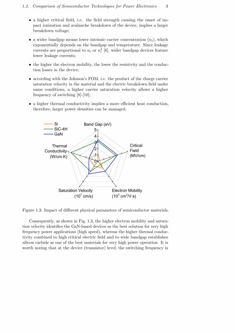
1.2. Comparison of Semiconductor Technologies for Power Electronics 3
• a higher critical field, i.e. the field strength causing the onset of im-pact ionization and avalanche breakdown of the device, implies a largerbreakdown voltage;
• a wider bandgap means lower intrinsic carrier concentration (ni), whichexponentially depends on the bandgap and temperature. Since leakagecurrents are proportional to ni or n2i [6], wider bandgap devices featurelower leakage currents;
• the higher the electron mobility, the lower the resistivity and the conduc-tion losses in the device;
• according with the Johnson’s FOM, i.e. the product of the charge carriersaturation velocity in the material and the electric breakdown field undersame conditions, a higher carrier saturation velocity allows a higherfrequency of switching [8]-[10];
• a higher thermal conductivity implies a more efficient heat conduction,therefore, larger power densities can be managed.
012345
ThermalConductivity
(W/cm K)
Saturation Velocity(107 cm/s)
Electron Mobility(103 cm2/V s)
CriticalField (MV/cm)
Band Gap (eV) Si SiC-4H GaN
Figure 1.3: Impact of different physical parameters of semiconductor materials.
Consequently, as shown in Fig. 1.3, the higher electron mobility and satura-tion velocity identifies the GaN-based devices as the best solution for very highfrequency power applications (high speed), whereas the higher thermal conduc-tivity combined to high critical electric field and to wide bandgap establishessilicon carbide as one of the best materials for very high power operation. It isworth noting that at the device (transistor) level, the switching frequency is

4 Chapter 1. Introduction
mainly limited by the intrinsic capacitances of the device structure. However,as discussed in the next section, the better trade-off between breakdown voltageand ON-resistance allows a smaller GaN-based structure compared to Si-basedone, having hence smaller capacitances. Finally, in the case of low power andlow speed applications, Si-based devices are still preferred to SiC and GaNcompetitors because of the higher reliability and low cost due to technologymaturity, discussed in the following chapters.
1.2.1 Theoretical limit of Si, SiC and GaN power FETs
An ideal power device should be characterized by a high switching frequency,good heat dissipation properties, a small ON-resistance and a large breakdownvoltage. However, with reference to a conventional vertical power FET [11],while the switching speed and the thermal resistance are mainly dependent onthe intrinsic capacitances of the structure, hence device dimensions and relativepermittivity of the adopted materials, and by the thermal conductivity of thematerials, respectively, in the case of ON-resistance and breakdown voltage amutual dependence exists.
Figure 1.4: (a) Conventional vertical power MOSFET and (b) its electric fielddistribution in the drift region.
The maximum voltage (breakdown voltage) that a power device can supportbefore the onset of a significant current flow is limited by the avalanchebreakdown phenomenon caused by carrier multiplication by impact ionization.This latter occurs as the electron–hole pairs created by a carrier traversingthe depletion layer and heated by a large electric field [11]. Consequently, theimpact ionization and hence the breakdown voltage are strongly dependenton the magnitude of the electric field. The minimum value determining theavalanche breakdown phenomenon is named critical electric field (EC) and ischaracteristics of each semiconductor material, as it is an increasing function

1.2. Comparison of Semiconductor Technologies for Power Electronics 5
of bandgap.
The unipolar power devices, deeply discussed in the following sections,feature a drift region aimed at supporting the blocking voltage. Its propertiescan be analyzed by assuming an abrupt junction (P+N) with high dopingconcentration on one side and a low uniform doping concentration on the otherside as shown in Fig. 1.4. According to Poisson’s equation, the maximumelectric field (Emax) can be described as follows:
Emax =qNDWD
ε0εr(1.1)
Breakdown occurs when Emax = EC and VDS equals the breakdown voltage(BV ). BV can be approximately evaluated as the voltage drop across thedepletion region
BV =1
2ECWD =
1
2
qNDW2D
ε0εr(1.2)
where EC , ε0, εr, ND, and WD are the critical electric field, vacuum permittivity,relative permittivity of the semiconductor, doping concentration and maximumdepletion width of the drift region, respectively. In the ON-state operationmode, the specific ON-resistance (RON,sp) associated to the drift region canbe modeled as follows:
RON,sp = ρWD =WD
qµnND(1.3)
where ρ and µn are the resistivity and the electron mobility, respectively. Byreplacing ND and WD by the expressions in Eq. 1.1 and 1.2, the so-calledBaliga figure of merit (BFOM) [8] is attained:
RON,spBV 2
=4
ε0εrµnE3C
(1.4)
As shown in Eq. 1.4 the ratio of RON,sp to BV 2 is fixed by the intrinsicproperties of the material. As a result, by considering the material parametersreported in Table. 1.1 for silicon, silicon carbide and gallium nitride, thecorresponding theoretical limits can be extracted as shown in Fig. 1.5 (lines).
Material Ec (MV/cm) µn (cm2/V s) εrSi 0.23 1350 11.8
SiC 2.2 950 9.7
GaN 3.3 1800 9
Table 1.1: Material properties of Si, SiC and GaN [12].
It is worth noting that real semiconductor devices (symbols) are generallyfar from ideal structures and so it is always a challenge to achieve the theoretical

6 Chapter 1. Introduction
limit. In particular, the channel mobility in real devices is lower than bulk (Siand SiC) mobility reported in Table 1.1 because of the surface scattering and/orhigh electric field related mechanisms, whereas the channel 2DEG mobility inGaN device is mainly reduced because of the process-related degradation underthe gate area. Moreover, the theoretical limit is calculated by consideringonly the resistive contribution of the drift region whereas the real devices areaffected by additional resistive effects contributing to the overall ON-resistance,especially in the low voltage field.
101 102 103 10410-1
100
101
102
103
Si Si-SJ SiC GaN HFET
RO
N,s
p (m
cm2 )
BV (V)
Figure 1.5: Specific ON-resistance per unit area as a function of the breakdownvoltage for silicon, silicon carbide and gallium nitride. Theoretical limits (lines)and experimental data reported in [16] (symbols).
By observing Fig. 1.5 it is possible to notice that: i) the silicon FETsshow more severe limitation compared to SiC and GaN counterparts. Byincreasing the voltage rating, Si-based devices provide less efficient electronicsapplications because of the higher resistance, hence higher conduction losses.As a result, for voltage range higher than about 200 V, GaN- and SiC-baseddevices seem to be preferable to silicon ones. Regarding the choice between SiCand GaN, as partially anticipated in Fig. 1.3, others factors like temperaturehandling, switching frequency and cost have a major impact; ii) by reducing thebreakdown voltage, real devices (see Si-based devices in Fig. 1.5) show a largerresistance compared to its limit because, as previously anticipated and deepenedlater, additional resistive components start to give an important contribution tothe overall RON ; iii) GaN-on-Si devices are still far from own theoretical limitbecause the failure mechanisms are not due to avalanche breakdown occurringbetween drain and source but to vertical (buffer) breakdown occurring between

1.2. Comparison of Semiconductor Technologies for Power Electronics 7
drain and substrate caused by the presence of defects due to lack of maturityprocess [13]-[15].
1.2.2 Si-based Power MOSFETs
The first commercially available power MOSFET was developed by using avertical double-diffusion process. The vertical structure was necessary in orderto withstand high voltages and currents required by a power circuit. Thanks tothis approach drain and source are located on the opposite sides of the waferallowing the use of thicker metal fingers (drain and source) compared to thelateral structure, where these latter must be interdigitated [11]. In addition,the electric field/potential distribution within the vertical structure is moreappropriate for supporting high voltages.
The vertical-diffused (VD)-MOSFET structure is shown in Fig. 1.6. With-out the application of a gate bias, a high positive voltage can be sustainedbetween drain and source. In this case, junction J1 formed between the P-baseand the N-drift region becomes reverse biased and the applied voltage is mainlysupported by the lowly doped N-drift region.
Figure 1.6: Vertical-diffused (VD)-MOSFET structure.
By applying a positive gate bias (VG > VTH) the channel is formed at theP-base/Oxide interface, providing a current path from the drain to the sourcewhen a positive drain voltage is applied. After drifting from the source regionthrough the channel, the electrons are confined in a narrow JFET region locatedbetween the adjacent P-base regions within the VD-MOSFET structure. Thehigher is the applied drain voltage the thinner is the JFET region because ofthe wider depletion regions of the reverse biased junctions J1. As a result, thiscurrent confinement increases the internal resistance. Moreover, after being

8 Chapter 1. Introduction
transported through the JFET region, the current spreads from the narrowJFET region to the entire width of the N-drift section. This nonuniform currentdistribution increases the ON-resistance, making it larger than the ideal valuesof the drift region [11].
In order to reduce series resistance, an alternative device structure calledtrench-gate or U-MOSFET was developed by adopting a trench technology. Asshown in Fig. 1.7 the trench extends from the upper surface of the structure tothe N-drift region avoiding the JFET region. Consequently, the U-MOSFETstructure offers the opportunity to reduce the internal resistance of the powerMOSFET closer to the ideal value and to increase the cell density. Moreover,subsequent structure optimizations improved also the operating frequency forpower MOSFETs up 1-MHz range [11].
Figure 1.7: Trench-gate or U-MOSFET structure.
Taking into account the discussion of Section 1.2.1, it is evident that thehigher is the breakdown voltage the higher and more dominant is the resistivecontribution of the N-drift region. Consequently, this kind of structure are notinclined to very high voltages. On the other hand, by observing Figs. 1.6 or1.7 it is possible to observe that by reducing the breakdown voltage, thus theN-drift resistance, other resistive components such as channel, accumulation,source/drain contacts, may become dominant avoiding to follow the theoreticallimit (see Fig. 1.5).
In order to guarantee larger breakdown voltages with lower ON-resistancesthan a conventional power MOSFET, a new architecture named superjunction(SJ)-MOSFET has been implemented (Fig. 1.8).

1.2. Comparison of Semiconductor Technologies for Power Electronics 9
Figure 1.8: Superjunction (SJ)-MOSFET structure.
The principle behind the blocking voltage is different from that for thepower MOSFET structures previously described. In this case, when a positivedrain bias is forced in absence of an applied gate voltage, depletion regionsare formed across the vertical junction J2 and the horizontal MOS interfacecreating the desired two-dimensional charge-coupling phenomenon [17], andthe horizontal junction J3 creating the two-dimensional depletion phenomenon[17].
Figure 1.9: (a) The ideal drift region and its electric field distribution (con-ventional vertical power MOSFET), (b) basic charge coupled structure and itselectric field distributions (SJ-MOSFET).

10 Chapter 1. Introduction
Consequently, the electric field distribution along the y-direction is alteredfrom the triangular shape (Fig. 1.9a), observed in conventional junctions (VD-and U-MOSFET case), to a rectangular shape (Fig. 1.9b) (SJ-MOSFET)with a lower maximum field value for a given drain voltage. This allows tosupport a required blocking voltage over a shorter distance when comparedwith conventional power MOSFETs.
In addition, the doping concentration of the N-type drift region can bemade much higher than that of a VD- or U-MOSFET, allowing a reductionof the specific ON-resistance below the ideal theoretical limit at any desiredbreakdown voltage (see Si-SJ in Fig. 1.4).
It is worth noting that, nowadays, in order to further increase the blocking(breakdown) voltage, similar structures are being proposed by simply replacingsilicon with silicon carbide material [18], [19].
1.2.3 GaN-based High Electron Mobility Transistors (HEMTs)
High Electron Mobility Transistors (HEMTs) are based on an AlGaN/GaNheterostructure able to form a sheet of electrons with high density and mo-bility thanks to its intrinsic properties. In particular, because of a differentelectronegativity between gallium (Ga) and nitride (N), both AlGaN and GaNfeature a spontaneous polarization as a bulk property. Moreover, the smallerlattice constant (aluminum concentration dependent) of the AlGaN inducesa piezoelectric polarization due to mechanical stress (strain) occurring whenthe thin AlGaN layer is grown on the top of the GaN. Consequently, due tothe charge compensation, a sheet of electrons is attracted at the AlGaN/GaNinterface forming the so-called 2-dimensional electron gas (2DEG) [20], [21].
Figure 1.10: Band diagram showing the surface donor state in the case ofundoped AlGaN barrier thickness (a) thinner than, and (b) thicker than thecritical thickness for the formation of the 2DEG [22].
However, the origin of this negative charge is not so clear due to the absenceof any intentional doped layer. The most accepted physical explanation consistsin the presence of donor states at the AlGaN surface able to provide the source

1.2. Comparison of Semiconductor Technologies for Power Electronics 11
of electrons for the 2DEG channel [21]. As a result, the thickness of the AlGaNlayer play a fundamental role in the formation of the 2DEG. After a criticalthickness, depending on the polarization contributions, the donor states crossthe Fermi level (see Fig. 1.10b) and provide negative charge aimed at formingthe 2DEG. More information on the physics of the 2DEG formation can befound in [20]-[22].
Due to the unavailability of large wafer size (above two inches) and highquality GaN bulk substrates, different solutions have been considered in orderto grow the AlGaN/GaN heterostructure on top of foreign substrates. Today,many research groups have been fabricating GaN-based devices on large-areasilicon substrates [23], [24] in order to guarantee a low-cost production.
Figure 1.11: Conventional structure of a depletion-mode high electron mobilitytransistor (HEMT).
A typical structure of the GaN-based HEMT is shown in Fig. 1.11. Dif-ferently from Si-based MOSFETs, GaN HEMTs feature a lateral structurewith two ohmic contacts (source and drain) connected to the 2DEG via alow-resistance path, and a Schottky gate contact on top of the AlGaN barrierable to modulate the 2DEG concentration by depleting or enhancing the chargedensity below the gate.
The huge difference in terms of thermal expansion coefficients and thelarge lattice mismatch occurring between GaN and silicon crystal, requires theepitaxial growth of an intermediated buffer ensuring a gradual variation ofthese properties along the stack aimed at avoiding the formation of cracks inthe AlGaN/GaN heterostructure.
A relevant issue, limiting the adoption of GaN devices in power applications,is the negative threshold voltage (depletion-mode) due to the spontaneousformation of the electrons channel. On the other hand, power electronicsapplications require enhancement-mode devices for safety, power consumptionand cost reasons [7].
To overcome this issue, several techniques have been developed to makenormally-OFF GaN-based transistors. Interesting results come from HEMTstructures in which a particular interlayer is placed between the heterostructure

12 Chapter 1. Introduction
and the gate contact, allowing to change the threshold voltage behavior and toenhance the positive swing of the gate terminal. In particular, MIS- and/orMOS-HEMTs, shown in Fig. 1.12a, are based on a deep barrier recess under thegate region [24], [25].With this solution the AlGaN barrier thickness is reducedbelow its critical thickness and, as previously discussed, the 2DEG formation isnot allowed under the gate. Fig. 1.12b shows the structure of a p-gate HEMT.By introducing a p-type gate (pGaN or pAlGaN) the conduction band of thegallium nitride (GaN) in the channel is pulled up, opposing to the formationof the 2DEG [27]. However, these additional layers lead, as discussed in thisthesis, to degradation mechanisms which need to be studied further.
Figure 1.12: (a) Metal-oxide-semiconductor (MOS)-HEMT and (b) p-type gateHEMT structure.
1.3 Role of Switching Power Devices in ElectronicsApplications
By considering low voltage electronics applications (≤ 200 V), an example ofthe most common and probably the simplest power stage topology, based onswitching mode semiconductor power devices, is the DC-DC buck (step-down)converter [28] shown in Fig. 1.13. It is wort noting that this example is onlyaimed at introducing the role and the required features of the transistor anddiode within a possible real electronics application and not at fully explainingthe theory behind the DC-DC converter.

1.3. Role of Switching Power Devices in Electronics Applications 13
Figure 1.13: Circuit schematic of a simplified buck (step-down) converter whichallows for the down-conversion of DC voltage.
Buck converter is a power supply which steps down voltage (while steppingup current) from its input (supply) to its output (load) with conversion efficiencyclose to 90 % [29]. The relationship between input and output voltage, underthe hypothesis of continuous conduction mode operation, is given by Eq. 1.5:
VOUT = VINtONTS
= VIND (1.5)
where tON , TS and D are the transistor ON-time during each switching cycle,the switching period and the duty-cycle, respectively. It is worth noting thatbeing D a number between 0 and 1 it is evident that VOUT will be always loweror at least equal to VIN .
Power electronics designers choose the buck converter because the outputvoltage has always the same polarity of the input voltage. Moreover, the outputis not isolated from the input meaning that they can share a common groundreducing the circuit complexity, hence area and cost.
By referring to Fig. 1.13, the circuit includes a controlled power switch,which usually is an enhancement mode (normally-OFF) transistor for safety,power consumption and cost reasons [7], a so-called freewheeling Schottkydiode, an inductor (L) and a capacitor (C) forming the output filter, and aresistor (ROUT ) representing the load. It is worth noting that a Schottky diodeis preferred with respect to other kinds of diode due to its lower forward voltageleading to lower power dissipation during ON-state operation and because ofthe reduced reverse recovery current.
When the transistor switches ON the circuit is reduced to Fig. 1.14. Thediode is reverse biased and the current through the inductor increases linearlyaccording to Faraday’s law. During this phase the supply provides energy,through the transistor, to the load and the inductor stores energy associatedto a magnetic field.
When the transistor is turned OFF a large voltage up to VIN is present atthe drain-source port, the energy flow coming from the supply is stopped andthe inductor starts to behave as a source thanks to the energy stored during

14 Chapter 1. Introduction
Figure 1.14: ON-state operation of buck converter. The transistor is in ON-state whereas the diode in OFF-state.
Figure 1.15: OFF-state operation of buck converter. The transistor is inOFF-state whereas the diode in ON-state.
the previous phase. At this time the voltage across the inductor reverts itspolarity, thus forcing the diode in forward mode and supplying the currentflow through the load as shown in Fig. 1.15.
The role of the freewheeling diode is crucial for the converter operationsince it avoids an abrupt current variation on the inductor when the transistoris switched OFF. In fact, given the relationship between the inductor (L), thevoltage (v(t)), and the current (i(t)):
v(t) = Lδi(t)
δt(1.6)
an abrupt change of the current can cause a huge voltage spike damaging theload or the other circuit components.
Based on the discussion on the roles played by switching mode semiconduc-tor power devices (transistor and diode) in an example of DC-DC converter, thepower losses might be analyzed in order to understand how the characteristicsof each device impact the performance and the efficiency of a power electronicscircuit.
The power loss of a switching circuit has two parts: static and dynamicpower loss. The static power loss is mainly determined by the ON-resistance of

1.4. Costs Comparison 15
the transistor and Schottky diode during the conduction mode. The dynamicpower loss occurs when the device (transistor and diode) switches from ON-state to OFF-state or vice versa. Consequently, devices with a fast switchingcapability and low recovery current are preferred to lower the dynamic powerdissipation.
In addition, a faster switching frequency allows to reduce the size of theinductor (L) and of the capacitor (C), improving the power density of thecircuit [30]. In order to understand this latter relationship, the output voltageripple (∆VOUT ) of the DC-DC buck converter may be considered. Under thehypothesis of continuous conduction mode operation, it can be calculated as:
∆VOUTVOUT
=1
8
T 2S(1−D)
LC=π2
2(1−D)
(fCfS
)2(1.7)
with switching frequency fS = 1/TS and corner frequency (fC):
fC =1
2π√LC
(1.8)
Equation 1.7 shows that the voltage ripple can be reduced by selecting acorner frequency (fC) of the output filter (LC) such that fC << fS . For agiven output voltage ripple (which is a key factor for DC-DC converters), theadoption of devices with a faster switching capability allows to use smallerpassive components such as inductor and capacitor.
In conclusion, it seems obvious that wide bandgap devices could be poten-tially preferred to silicon ones. However, to win a place in the power electronicsmarket, high performance is not enough since a low cost and a high level ofreliability has to be guaranteed. In the next sections, the different technologiesare compared in terms of costs and reliability.
1.4 Costs Comparison
Costs comparison between different technologies can be difficult since variouselements of cost such as starting material, epitaxial growth, wafer fabricationand assembly [12] must be taken into account. Nowadays, it is well know thatSiC-based devices feature a higher cost with respect to Si and GaN competitorsdue to the greater complexity of epitaxial growth and wafer fabrication [31],[32]. Therefore, the silicon technology is preferable, except for very high powerelectronics applications for which, as discussed in section 1.2, high thermalconductivity, critical field and wide bandgap are necessary.
Today, since GaN-based devices (transistors and Schottky diodes) with avoltage rating lower than about 600 V are mainly fabricated in thin (Al)GaNlayers grown on 200 mm standard silicon substrate [33]-[35], there is notsignificant cost difference with power Si-MOSFETs produced on a wafer of

16 Chapter 1. Introduction
the same diameter. However, by considering that GaN transistors, thanks tointrinsic material properties, are able to withstand larger current densitiescompared to Si competitors, the cost per function is further reduced [12].
Unfortunately, the huge difference in terms of thermal expansion coefficientsand the large lattice mismatch occurring between GaN and silicon crystal,requires the epitaxial growth of an intermediated buffer ensuring a gradualvariation of these properties along the stack. This latter can be formed bymultiple step-graded AlGaN buffers (Fig. 1.16a) with thickness up to few µm[36] or an AlN/GaN superlattice stack [37] (Fig. 1.15b) aimed at avoiding theformation of cracks in the GaN heterostructure. This is usually performedby means of metal-organic chemical vapor deposition (MOCVD) [38], whichprovides high quality buffer but at high costs due to the need of additional rawmaterials. Consequently, up to now GaN epitaxy on silicon is more expensivethan Si epitaxy. However, assuming the strong interest in manufacturingGaN-on-Si devices, it is expected that the cost of GaN epitaxy will approachthat of silicon [12].
Figure 1.16: Example of a structure stack with (a) a multiple step-gradedAlGaN and (b) an AlN/GaN superlattice buffer.
GaN-based devices are currently fabricated in high-productivity siliconCMOS facilities with processing temperatures similar to those of Si-competitors.Moreover, the GaN transistors structure is characterized by much fewer pro-cessing steps compared to silicon power MOSFETs [12]. As a result, the costis reduced and it may become lower as the GaN transistor production volumesgrow.
Finally, GaN-based devices can be packaged at a lower cost because of thelateral structure. In fact, they can be assembled in a wafer level chip-scalepackage (WLCSP) with terminals in a land grid array (LGA) [12] withoutcompromising the electrical, thermal, or reliability characteristics. On the otherhand, in the case of Si power MOSFETs, electrical package connections need

1.5. Reliability Issues 17
to be made to the top and bottom because of the vertical structure, increasingthe package complexity and the cost.
In conclusions, by analyzing starting material, epitaxial growth, waferfabrication and assembly costs it may be expected that GaN-based powerdevices can be fabricated at comparable or even, as expected for the future,lower costs compared to Si-based power transistors. However, it is worth notingthat, nowadays, in order to increase the device voltage rating above 600 V othersubstrates such as SiC, AlN, etc. are required and still under investigation interms of reliability and cost.
1.5 Reliability Issues
In the case of power devices, reliability is the most crucial and often themost challenging characteristic to be guaranteed in combination with highperformance and low cost.
The Institute of Electrical and Electronics Engineers (IEEE) defines re-liability as ”the ability of a system or component to perform its requiredfunctions under stated conditions for a specified period of time” [39]. In thesemiconductor power devices area the expected lifetime before failure usuallyranges between 10 and 20 years.
Semiconductor device reliability may be related to different process aspectssuch as: i) undesired impurities due to many process steps adopted duringfabrication phase; ii) thin layers deposition; iii) introduction of new materialand processes; iv) assembly and environmental conditions, etc. Consequently,each of these factors can induce one or more failure mechanisms affecting thedevice reliability.
Before analyzing in detail the induced failure mechanisms it is really im-portant to understand how and when the device reliability can be affected.By considering the buck DC-DC converter shown in Fig. 1.13 it is possible tosummarize that:
• when the converter is in ON-state operation mode (Fig. 1.14) the tran-sistor is in ON-state regime whereas the diode is reversely biased. Inthis phase, the transistor has to handle a moderate positive (normally-offtechnology) gate voltage aimed at allowing a high current flow betweendrain and source. As a result, the moderate gate bias, the high draincurrent and the high channel temperature due to self-heating effects maytrigger degradation mechanisms, generally induced by charge trappingand/or electron migration phenomena [40], [41], affecting the transistorreliability. Concerning the diode, it must withstand a high reverse voltageinducing high electric fields degrading the device;
• when the converter is in OFF-state operation mode (Fig. 1.15) thetransistor is switched-OFF whereas the diode is in forward regime. In

18 Chapter 1. Introduction
this case the transistor is subject to a high drain voltage (high electricfield) promoting the creation or activation of defects degrading deviceperformance [42]. On the other hand, the diode has to handle highforward currents; under this condition the combined effect of high current,moderate electric field and high junction temperature can affect the diodereliability;
• finally, a third operation condition, called semi-on-state, occurs duringthe switching transient. In this phase, the transistor operates with smalloutput current and moderate drain bias. As a result, electrons presentin the channel can be accelerated by the applied electric field becoming”hot electrons ” and triggering trapping mechanisms [43].
Since the reliability analysis involves phenomena whose time-scale is inthe order of many years, accelerated test methods have to be adopted inorder to evaluate the device lifetime and to identify the involved degradationmechanisms in a reasonable time. Using temperature, voltage, current, andhumidity as acceleration factors [44], failure can be induced earlier than usualand with the adoption of extrapolation methods the lifetime under nominaloperation mode can be estimated. It is therefore evident the relevance ofresearch on device reliability issues: without a correct investigation aimedat understanding the physical mechanisms inducing device degradation andfailure, the reliability predictions are expected to become meaningless and theempirical estimations will be very inaccurately related to process modifications,device geometry, voltage and current ratings.
In this thesis, the experimental characterization of degradation mecha-nisms induced by ON-state stress and affecting the reliability of Si-basedpower U-MOSFETs, GaN-based Schottky diodes and transistors are investi-gated. Moreover, TCAD simulations aimed at understanding the sources ofdegradation are performed in combination to experimental tests.
1.6 Outline of the Thesis
This dissertation is organized as follows:
• Chapter 2 shows the results of an activity developed in collaboration withSTMicroelectronics inside an European project named ”E2SG Energyto smart grid”. The purpose was the investigation of the degradationmechanisms induced by negative bias temperature instability (NBTI) intrench-gated p-channel power Si-MOSFETs (U-MOSFETs). Hence, vari-ous measurements techniques have been adopted in order to distinguishinterface and bulk-oxide traps and a combined measurement/simula-tion method, aimed at estimating the spatial and energy oxide trapdistribution, has been implemented;

1.6. Outline of the Thesis 19
• Chapter 3 is focused on the results obtained inside an European projectnamed ”E2COGaN Energy Efficient Converters using GaN Power De-vices”. A physical model interface (PMI), accounting for the temperaturedependence of the thermal boundary resistance (TBR) associated tothe heterojunction transition layer, has been implemented by meansof Sentaurus TCAD in order to realistically model self-heating effects.In particular, TBR associated to the nucleation layer between GaNand SiC- or Si-substrate was taken into account and the influence ofthe temperature on the surface charges trapping and de-trapping wasinvestigated;
• Chapter 4 describes the results of an activity developed in collaborationwith the interuniversity microelectronics centre (imec). A combinedmeasurement/simulation analysis has been performed in order to un-derstand the degradation mechanisms induced by ON-state stress inGaN-based Schottky barrier diodes (SBDs). In particular, by analyz-ing the geometry dependence, the physical mechanisms responsible forlong-term degradation of SBDs have been identified;
• Chapter 5 reports the results of an experimental activity performedin collaboration with imec. The time-dependent breakdown, inducedby forward gate stress in GaN-based power HEMTs with p-type gate,has been analyzed. In particular, the mechanisms underlying the gatebreakdown and its effects on the device performance have been inves-tigated by adopting different stress conditions, analyzing the influenceof the temperature, and investigating the activation energy of the traps.In addition, an original empirical model, representing the relationshipbetween gate leakage current and time to failure, has been proposed.
• Chapter 6 summarizes the main achievements of this PhD researchproject.
References
[1] X Luo, J. Wang, M. Dooner, J. Clarke, ”Overview of current developmentin electrical energy storage technologies and the application potential inpower system operation,” Journal of Appl. Energy, Vol. 137, pp. 511-536,Jan. 2015.
[2] B. K. Bose, ”Energy, environment and importance of power electronics,”Proc. IEEE Powering Conf., pp. 38-47, Setubal, Portugal, Apr. 2007.
[3] Z. Stevic, I. Radovanovic, ”Energy efficiency of electric vehicles,” NewGeneration of Electric Vehicles, pp. 93-134, DOI:10.5772/55237, Dec. 2012.
[4] J. Hu, ”Performance optimization and long term stability of integratedGaN diodes,” ESAT-MICAS, Microelectronics and Sensors, 2016.
[5] T. Kimoto, ”Ultra-high voltage devices for future power infrastructure,”www.compoundsemiconductor.net, Apr. 2014.
[6] N. Kaminski, ”State of the art and the future of wide band-gap devices,”IEEE Proc. in Power Electronics and Applications Conf., Sept. 2009.
[7] J. Millian, P. Godignon, X. Perpina, A. Perez-Tomas, J. Rebollo, ”Asurvey of wide bandgap power semiconductor devices,” IEEE Transactionon Power Electronics, Vol. 29, No. 5, pp. 2155-2163, May 2014.
[8] B. J. Baliga, ”Power semiconducto device figure of merit for high-frequencyapplications,” IEEE Electron Device Letter, Vol. 10, No. 10, pp. 455-457,1989.
[9] A. Johnson, ”Physical limitations on frequency and power parameters oftransistors,” RCA Review, Vol. 26, pp. 163-177, 1965.
[10] F. A, Marino, N. Faralli, D. K. Ferry, S. M. Goodnick, and M. Saraniti,”Figures of merit in high-frequency and high-power GaN HEMTs,” Journalof Physics, Vol. 193, pp. 1-4, 2009.
[11] B. J. Baliga, ”Fundamentals of power semiconductor devices,” Springer,ISBN 978-0-387-47313-0, 2008.
20

References 21
[12] A. Lidow, J. Strydom, M. de Rooij, D. Reusch, ”GaN transistors forefficient power conversion,” Second Edition, WILEY, ISBN: 978-1-118-84479-3, Set. 2015.
[13] B. Lu, E. L. Piner, and T. Palacios, ”Breakdown mechanism in Al-GaN/GaN HEMTs on Si substrate,” Proceedings of the Device ResearchConference (DRC), pp. 193-194, Jun. 2010.
[14] C. Zhou, Q. Jiang, S. Huang, K. J. Chen, ”Vertical leakage/breakdownmechanisms in AlGaN/GaN-on-Si devices,” IEEE Electron Device Letters,Vol. 33, No. 8, pp. 1132-1134, Aug. 2012.
[15] S. Yang, Q. Jiang, B. Li, Z. Tang, K. J. Chen, ”GaN-to-Si verticalconduction mechanisms in AlGaN/GaN-on-Si lateral heterojunction FETstructures,” Phycisa Status Solidi (C), Vol. 11, No. 3-4, pp. 949-952, Apr.2014.
[16] N. Ikeda, Y. Niiyama, H. Kambayashi, Y. Sato, T. Nomura, S. Kato,and S. Yoshida, ”GaN power transistors on Si substrates for switchingapplications,” Proceedings of the IEEE, Vol. 98, No. 7, pp. 1151-1161, Jul.2010.
[17] B. J. Baliga, ”Advanced power MOSFET concepts,” Springer, ISBN978-1-4419-5916-4, 2010.
[18] Y. Wang, K. Tian, Y. Hao, C. H. Yu, Y. J. Liu, ”4H-SiC step trench gatepower metal-oxide-semiconductors field-effect transistor,” IEEE Transac-tions on Electron Devices, Vol. 37, No. 5, pp. 633-635, May 2016.
[19] L. Yu and K. Sheng, ”Modeling and optimal device design for 4H-SiCsuper-junction devices,” IEEE Transactions on Electron Devices, Vol. 55,No. 8, pp. 1961-1969, Aug. 2008.
[20] O. Ambacher, J. Smart, J. R. Shealy, N. G. Weimann, K. Chu, M. Murphy,W. J. Schaff, L. F. Eastman, R. Dimitrov, L. Wittmer, M. Stutzmann,W. Rieger, and J. Hilsenbeck, “Two-dimensional electron gases inducedby spontaneous and piezoelectric polarization charges in N- and Ga-faceAlGaN/GaN heterostructures,” Journal of Applied Physics, Vol. 85, No.6, pp. 3222-3233, 1999.
[21] O. Ambacher, B. Foutz, J. Smart, J. R. Shealy, N. G. Weimann, K. Chu,M. Murphy, A. J. Sierakowski, W. J. Schaff, and L. F. Eastman, “Twodimensional electron gases induced by spontaneous and piezoelectric po-larization in undoped and doped AlGaN/GaN heterostructures,” Journalof Applied Physics, Vol. 87, No. 1, pp. 334-344, 2000.
22 References
[22] J. Ibbetson, P. Fini, K. Ness, S. DenBaars, J. Speck, and U.Mishra, ”Polar-ization effects, surface states, and the source of electrons in AlGaN/GaNheterostructure field effect transistors,” Applied Physics Letters, Vol. 77,No. 2, pp. 250–252, 2000.
[23] K. Cheng, H. Liang, M. Van Hove, K. Geens, B. De Jaeger, P. Srivastava,X. Kang, P. Favia, H. Bender, S. Decoutere, ”AlGaN/GaN/AlGaN doubleheterostructures grown on 200 mm silicon (111) substrates with highelectron mobility,” Applied Physics Express, Vol. 5, No. 1, p. 011002, 2011.
[24] D. Christy, T. Egawa, Y. Yano, H. Tokunaga, H. Shimamura, Y. Yamaoka,A. Ubukata, T. Tabuchi, and K. Matsumoto, ”Uniform growth of AlGaN/-GaN high electron mobility transistors on 200 mm silicon (111) substrate,”Applied Physics Express, Vol. 6, No. 2, p. 026501, 2013.
[25] Y. Shi, S. Huang, Q. Bao, X. Wang, K. Wei, H. Jiang, J. Li, C. Zhao, S.Li, Y. Zhou, H. Gao, Q. Sun, H. Yang, J. Zhang, W. Chen, Q. Zhou, B.Zhang, and X. Liu, “Normally OFF GaN-on-Si MIS-HEMTs fabricatedwith LPCVD-SiNx passivation and high-temperature gate recess,” IEEETransaction on Electron Devices, Vol. 63. No. 2, pp. 614-619, Feb. 2016.
[26] J. Wu, W. Lu, P. K. L. Yu, “Normally-OFF AlGaN/GaN MOS-HEMTwith a two-step gate recess,” IEEE International Conference on ElectronDevices and Solid-State Circuits, pp. 594-596, Singapore, Jun. 2015.
[27] O. Hilt, F. Brunner, E. Cho, A. Knauer, E. Bahat-Treidel, and J. Wurfl,“Normally-off High-Voltage p-GaN Gate GaN HFET with Carbon-DopedBuffer,” IEEE International Symposium on Power Semiconductor Devices& IC’s, pp. 239-242, San Diego, May 2011.
[28] E. Rogers, ”Understanding buck power stages in switching mode powersupplies,” Texas Instruments, Mar. 1989.
[29] ”AN0948: Power configurations and DC-DC,” Silicon Labs, Jun. 2016.
[30] R. Nowarowski, B. King, ”Challenges of designing high-frequency, high-inpu-voltage DC/DC converters,” Texas Instruments, Analog ApplicationsJournal, Vol. 20, pp. 28-31, 2011.
[31] P. Friedrichs, T. Kimoto, L. Ley, G. Pensl, ”Silicon Carbide, Volume2: Power Devices and Sensors,” WILEY, ISBN: 978-3-527-40997-6, Oct.2009.
[32] S. E. Saddow, A. Agarwal, ”Advances in silicon carbide processing andapplications,” Artech House, Inc., ISBN: 1-58053-740-5, 2004.

References 23
[33] D. Marcon, Y. N. Saripalli, S. Decoutere, ”200mm GaN-on-Si epitaxy ande-mode device technology,” IEEE International Electron Devices Meeting(IEDM), pp. 414-417, Washington, Dec 2015.
[34] K. H. Lee, S. Bao, L. Zhang, D. Kohen, E. Fitzgerald, and C. S. Tang,”Integration of GaAs, GaN, and Si-CMOS on a common 200mm Si sub-strate through multilayer transfer process,” Applied Physics Express, Vol.9, No. 8, Jul 2016.
[35] J. Cheng, X. Yang, L. Sang, L. Guo, J. Zhang, J. Wang, C. He, L. Zhang,M. Wang, F. Xu, N. Tang, Z. Qin, X. Wang, B. Shen, ”Growth of highquality and uniformity AlGaN/GaN heterostructures on Si substrate usinga single AlGaN layer with low Al composition,” Nature, Vol. 6, No. 23020,Mar 2016.
[36] S. Tripathy, V. K. X. Lin, S. B. Dolmanan, J. P. Y. Tan, R. S. Kajen, L.K. Bera, S. L. Teo, M. K. Kumar, A. Arulkumaran, G. I. Ng, S. Vicknesh,S. Todd, W. Z. Wang, G. Q. Lo, H. Li, D. Lee, S. Han, ”AlGaN/GaN two-dimensional-electron gas heterostructures on 200mm diameter Si(111),”Applied Physics Letters, Vol. 101, No. 082110, pp. 1-5, 2012.
[37] Y. Ni, L. He, D. Zhou, Z. He, Z. Chen, Y. Zheng, F. Yang, Z. Shen,X. Zhang, L. He, Z. Wu, B. Zhang, Y. Liu, ”Low-leakage current andhigh-breakdown voltage GaN-on-Si (111) system with an AlGaN impurityblocking layer,” Journal of Materials Science, Vol. 27, No. 5, pp. 5158-5163,May 2016.
[38] K. Matsumoto, Y. Yamaoka, A. Ubukata, T. Arimura, G. Piao, Y. Yano,H. Tokunaga, T. Tabucchi, ”Opportunities and challenges in GaN metalorganic chemical vapor deposition for electron devices,” Japanese Journalof Applied Physics, Vol. 55, No. 5S, pp. 05FK04.1-05FK04.4, Apr. 2016.
[39] ”610-1990 - IEEE Standard Computer Dictionary: A Com-pilation of IEEE Standard Computer Glossaries,” IEEE, DOI:10.1109/IEEESTD.1991.106963, Jan. 1991.
[40] M. Ohring, ”Reliability and failure of electronic materials and devices”,Academic Press, pp. 237- 292, 1998.
[41] R. Coffie, Y. Chen, I. P. Smorchkova, M. Wojtowicz, Y. C. Chou, B. Heying,and A. Oki, ”Impact of AlN interlayer on Reliability of AlGaN/GaNHEMTs,” IEEE International Reliability Physics Symposium, pp. 99-102,Mar. 2006.
[42] T. Ohki, T. Kikkawa, Y. Inoue, M. Kanamura, N. Okamoto, K. Makiyama,K. Imanishi, H. Shigematsu, K. Joshin, and N. Hara, ”Reliability of GaN

24 References
HEMTs: Current status and future technology,” IEEE InternationalReliability Physics Symposium, pp. 61-70, Apr. 2009.
[43] G. Meneghesso, G. Verzellesi, F. Danesin, F. Rampazzo, F. Zanon, A.Tazzoli, M. Meneghini, and E. Zanoni, ”Reliability of GaN High ElectronMobility Transistors: state of the art and perspectives”, IEEE Transactionon Device and Material Reliability, Vol.8, No. 2, pp. 332-342, 2008.
[44] ”Power Semiconductor Reliability Handbook,” Alpha&Omega Semicon-ductor, www.aosmd.com, USA, 2010.

Chapter 2
NBTI Reliability in Si-based PowerU-MOSFETs
2.1 Introduction and State of the Art
Negative Bias Temperature Instability (NBTI) [1] is one of the main degradationmechanisms limiting the long-term reliability of power MOSFETs biasedabove threshold [2], [3]. The same effect is also referred to as Negative BiasTemperature Stress (NBTS) or High Temperature Gate Bias (HTGB) andis commonly observed in p-channel devices when stressed with negative gatevoltages at elevated temperatures. In particular, when a large gate voltagecombined with a high temperature is applied and the other terminals areshort circuited to ground or held to the same potential, charge trapping andinterface states generation mechanisms occur in the bulk gate oxide and at thesemiconductor/oxide interface, respectively [4], [5]. These phenomena lead toa degradation of electrical parameters such as threshold voltage (VTH), chargecarrier mobility, ON-resistance, trans-conductance and sub-threshold slope [1],which are important figures of merit characterizing a power MOSFET.
The interface states (Nit) generation is usually ascribed to the breakingof SiH bonds at the SiO2/Si interface by a combination of electric field,temperature and holes effects [4], whereas the build-up of positive oxide charge(Not), may be due to H+ de-passivation [5] or hole trapping. However, thedetails how NBTI occurs and how it can be recoverable are not entirely clear.
Different models, by different groups, have been proposed on NBTI relatedphysical mechanisms. A stress time linear-dependent SiO2/Si interface trapsgeneration has been suggested in [6]-[8] by means of a Reaction-Diffusion (R-D)model. In particular, hydrogen is released during reaction phase and thendiffused from interface to oxide (diffusion phase) with a time dependence oft0.25. Grasser et al. in [9] have proposed a four-energy-well model accountingfor the coupled contribution of interface states and oxide traps. Instead, for[10] the NBTI phenomenon is ascribed to uncorrelated contribution of the
25

26 Chapter 2. NBTI Reliability in Si-based Power U-MOSFETs
interface states and oxide traps, suggesting that only the oxide defects areinvolved in the recovery mechanism. Finally, on the other hand, a fast trappingand de-trapping mechanism of the oxide defects, with a slow recovery of theinterface states, has been proposed by Mahapatra et al. [11].
Although many papers about NBTI reliability of CMOS technology havebeen published [12], [13], similar phenomenon affecting power MOSFETsreceived much less attention so far. However, as power devices are scaled downand large voltages are applied, NBTS together with the High TemperatureReverse Bias (HTRB), represent the main degradation mechanisms limitingthe long-term power device reliability.
Limited studies have been performed on power VD-MOSFETs in order tounderstand [14] and to overcome [15] NBTI induced degradation. In particular,in [16] the oxide-trapped charge build-up is attributed to hole tunneling fromthe silicon valence band to oxygen vacancy defects, whereas the interface stategeneration is due to the electro-chemical reaction of the interface precursorwith the charged oxide traps. Other studies, referred to as High TemperatureGate Bias (HTGB) but related to the same NBTI mechanisms, have beencarried out on different structures of power MOSFETs. In particular, in [3] isreported a study of SiC power MOSFETs in which the VTH shift is ascribedto the trapping and de-trapping of charge from the near interfacial oxide traps,whereas Aoki et al. [17] have treated a reliability study of trench gate powerMOSFET with partially thick gate oxide film structure.
In this chapter, the NBTI degradation mechanisms in p-channel Si-trenchpower MOSFETs, also referred to as U-MOSFET, is extensively analyzed byinvestigating the impact of gate stress (voltage and temperature) on the mainfigures of merit, such as threshold voltage, trans-conductance and subthresholdslope.
First of all, different methods for evaluating NBTI stress-induced thresholdvoltage shift (∆VTH) are considered and discussed in order to highlight thefast-partial recovery phase occurring during the characterization phase. Then,besides the analysis of the degradation occurring during the stress phase, therecovery phase happening after the removal of the gate bias stress is alsoinvestigated. This analysis is performed at different recovery voltages andtemperatures in order to understand how their contribution affects the recoveryphase. Thanks to this approach, it is possible to ascribe the threshold voltagerecovery, for the monitored time window, to the charge de-trapping frombulk oxide. Consequently, although various on-wafer techniques have beenproposed for estimating the oxide trap distribution [18], [19], they cannot beeasily applied in power U-MOSFETs, because of its vertical structure andbecause bulk and source terminals are often short-circuited. Therefore, inthis work a method based on a combination of DC measurements and TCADnumerical simulations has been implemented. As a result, the oxide trapdensity, including its energy distribution and its distance from the Si interface,

2.2. Device Structure and Experimental Setup 27
has been calculated by evaluating the VTH shift during the recovery phase.
2.2 Device Structure and Experimental Setup
Silicon-based p-channel power U-MOSFETs (Fig. 2.1), realized on-wafer by STMicroelectronics, are considered in this study. The gate stack is composed ofPolysilicon/SiO2/Silicon layers, the channel length is 0.5 µm, the equivalentchannel width is 69 cm and the oxide thickness is 40 nm. The device iscomposed by many fingers in parallel featuring of a maximum gate operationvoltage of -16 V.
Figure 2.1: A Schematic of a p-channel trench-gate power MOSFET. It featuresa gate stack composed of PolySi/SiO2/Si layer, a channel length of 0.5 µm,an equivalent channel width of 69 cm and an oxide thickness of 40 nm. TheU-shape of the gate allows the lowest ON-resistance (RON ) among all MOSstructure since JFET region is avoided.
This structural device architecture appears as the most suitable one forlow to medium voltage power applications because of the opportunity toreduce the internal resistance closer to the ideal value [20], hence offering thelowest possible ON-resistance among all MOS devices [21], [22]. In particular,compared to conventional VD-MOSFET structure, the JFET region is avoidedenabling a significant reduction of the overall specific ON-resistance. Moreover,the elimination of the JFET region allows a smaller cell pitch reducing theresistance contribution of channel, accumulation and drift regions [20].
On-wafer measurements were performed by means of a 200-mm Cascadeprobe station with an integrated Temptronic thermochuck able to warm upthe wafer till temperatures of 150◦C. Since the temperature is an acceleration

28 Chapter 2. NBTI Reliability in Si-based Power U-MOSFETs
factor for the degradation induced by NBTI stress [23], the use of a hightemperature allows to reach larger degradation in shorter times. In addition,Keithley System Measurement Units (SMUs) 26XX, controlled in a Lab-Viewenvironment, were used in order to force the bias stress/recovery and for IVmeasurements.
2.3 Measurements Techniques
Devices were stressed under NBTI, by applying a large gate voltage, and bygrounding drain and source terminals in order to have a uniform degradationalong the channel. After the stress a recovery phase was performed by forcinga gate bias equal or lower than threshold voltage. The temperature was keptconstant during both stress and recovery phases. The drain bias during themeasurement phases (both stress and recovery) was VDS = −25mV in orderto enforce the linear operation.
Figure 2.2: Electric field distribution along U-shape gate oxide in the case ofthe maximum stress condition VG = -24V. The rounded shape prevents thecreation of higher electric field in the proximity of corners.
The degradation due to NBTI was evaluated by mainly monitoring thethreshold voltage shift. Different bias conditions are considered during theNBTI stress. In order to determine the gate voltage to apply, TCAD numericalsimulations are performed, aiming at analyzing the electric field in the gateoxide. Because of the U-shape of the gate oxide, the uniformity of the electricfield must be verified. In Fig. 2.2 a TCAD Sentaurus simulation [24] performedon a U-MOSFET structure is reported. In particular, by observing the electricfield distribution in the gate oxide, it is possible to note as in the roundedregion the maximum electric field is similar to the one in the channel region.Since NBTI degradation is generally performed for electric field values between2 and 6 MV/cm [25], [26], having an oxide thickness of 40 nm, the following

2.3. Measurements Techniques 29
gate voltages were adopted during the stress: -16, -20, and -24V.
As typically reported in [27] for CMOS technology, also in the case ofU-MOSFETs the adopted method for evaluating the threshold voltage shiftsignificantly affects the dynamics of the VTH degradation. In fact, a partialrecovery occurs because of the measurement delay, during which the gate-biasis removed or reduced at low voltage. To this purpose, three measurementtechniques, namely IDVG-GMAX , Single Point (SP ), and On The F ly (OTF )were adopted in order to measure the threshold voltage. When these methodsare used to estimate the VTH shift during NBTI degradation, they differentlyaffect the fast recovery mechanism occurring during the measurement phase.
It is worth noting that, during the discussions of the different methods,the word ”recovery” is just referred to the fast recovery mechanism occurringduring the ID measurement phases when the gate stress is removed or reduced.
Besides the considered method, an IDVG measurement is required in freshdevices in order to estimate the trans-conductance (gm) and the thresholdvoltage (VTH−FRESH).
In the first method (IDVG-GMAX), the threshold voltage was evaluatedmy means of maximum trans-conductance method [28]. NBTI was applied bybiasing a constant gate voltage and the stress was periodically interrupted inorder to monitor the threshold voltage shift by measuring a full IDVG transfercharacteristic. The time delay, introduced by the measurement setup, occurringbetween the end of stress (removal gate bias) and the end of VTH measurement,was about 3 seconds. This method is widely used because it gives the possibilityto monitor the VTH , RON (mobility) and the subthreshold slope degradations.On the other hand, the VTH shift is estimated by considering the IDVG transfercharacteristic at VG values larger than VTH and hence it may be affected bymobility degradation.
In Single Point method, during the periodic interruption of the stress, thegate bias was reduced to VG ≈ VTH in order to minimize the recovery process[29], [30]. The VTH shift was estimated through the evaluation of ∆ID fordifferent stress times at VG ≈ VTH and VDS = −25mV . The time delay in thiscase was 29 ms, since a single drain current value was measured. The benefitof this method is due to the non-total removal of the stress voltage, whichallows to reduce the amount of recovery occurring during measurement phase,compared to the IDVG-GMAX case. In addition, the shorter measurement timeallows to evaluate the VTH shift with lower recovery. On the other hand, it isnot possible to monitor the degradations of other electrical parameters since asingle drain current value is measured.
Finally, in OTF method, the stress was not suspended at all, in order tocompletely avoid the recovery process, and the drain current was periodicallymonitored for VG = VSTRESS [31]. Since the gate bias was not removed formonitoring ∆ID, a series of repeated measurements were performed during thestress. As a result, the standard uncertainty of measurement was estimated.

30 Chapter 2. NBTI Reliability in Si-based Power U-MOSFETs
By considering a Gaussian distribution, the error bar (± 3 µ) guarantees a99.7 % confidence interval. For the other methods, single measurements wereconsidered since the repeated removal or reduction of the stress voltage wouldlead to a repeated fast recovery and hence to a non-correct evaluation of theNBTI induced degradation.
In the case of OTF method the VTH shift was calculated as:
∆VTH = −∆IDgm
(2.1)
where gm is the trans-conductance for VG equal to the stress voltage in freshdevice. The accuracy of this method is in general affected by the mobility/on-resistance degradation. In addition, the carrier mobility and subthreshold slopedegradation cannot be evaluated.
The threshold voltages shift occurring during NBTI stress, evaluated ac-cording to the different measurement techniques are reported in Fig. 2.3.
102 103 104 10510-3
10-2
10-1
Single Point Y = 0.0026X 0.26
IDVG_GMAX Y = 0.0013X0.31
On The Fly Y = 0.0164X 0.14
V TH
(V)
Stress Time (s)
Error Bar = ± 3µ
Stress Conditions VG = - 16 V T = 150°C
Method: Fitting:
Figure 2.3: VTH degradations, due to NBTI stress, evaluated with differenttechniques. The following stress conditions were considered: VG = -16 V, VDS= 0 V and T = 150 ◦C. During the measurement phases, VDS = -25 mV wasapplied in order to guarantee the operation in linear region.
It is worth noting that for each stress condition a single device has beenstressed. Therefore, the results reported from here on, are representative of asingle device.
The observed degradation is function of the method adopted for the VTHmeasurement, suggesting that when the gate-bias stress is suspended, a fast-partial degradation recovery occurs. In the case of OTF method, the gate-biasstress is not removed at all, hence no recovery occurs and the largest VTH shiftis observed. On the other hand, in the case of IDVG-GMAX method, the gatevoltage is reduced down to 0 during the measurement phase and a relatively

2.3. Measurements Techniques 31
long time delay (about 3 seconds) is required. This leads to a higher recoveryand thus to a lower VTH shift. Intermediate values are observed in the case ofSingle Point method, since, during the VTH measurement, the reduction ofVG to an intermediate value (close to VTH) and an intermediate time delay (29ms) is required. It may also notice that the results of the three methods tend toconverge as the total stress time increases. The hypothesis of recovery duringthe VTH measurement is supported by Fig. 2.4, in which the VTH recovery ismonitored for 2 s and is in qualitative agreement with the results reported in[32], [33] for p-CMOS technology. It is worth noting that a fast recovery of thethreshold voltage happens for t < 1s. The delay of 29 ms, reported in Fig. 2.4,is due to the limited speed of the experimental setup. However, according tothe large VTH shift observed in Fig. 2.3 for the OTF method, a further VTHincrease could be expected in Fig. 2.4 for t < 29 ms.
500 1000 1500 2000014,4
14,8
15,2
15,6
V TH (m
V)
Recovery Time (ms)
Error Bar = ± 3µ
Recovery Conditions:VG = VTHT = 150°C
29 ms
Figure 2.4: Threshold voltage recovery, evaluated by means of single pointmethod, after 1000 s of stress with VG = -16 V and T = 150 ◦C. During therecovery phase, the gate bias was chosen close to VTH . The first measurementtime (29 ms) is related to the limitations of the measurement setup. Otherpoints are an average over a fixed time window, and µ is the uncertainty.
In the remainder of this chapter the analysis will be focused on IDVG-GMAX method. Although a larger recovery occurs during VTH measurement,the acquisition of a complete IDVG transfer characteristic allows to evaluateother relevant electrical quantities, such as trans-conductance and subthresholdslope. These further parameters can be useful in order to better understandthe dynamics of interface states generation during the NBTI.
It is worth noting that from here on the word “recovery” will be consideredas the recovery phenomenon occurring from the end of stress when no biasesare applied on the device terminals.

32 Chapter 2. NBTI Reliability in Si-based Power U-MOSFETs
2.4 Results and Discussion
In Fig. 2.5 the threshold voltage shifts for different stress conditions (VG S)are shown. By increasing the stress voltage, a translation of ∆VTH curves isobserved, whereas the time exponent seems to be not affected by the stresscondition. This is in agreement with other studies reported in the literature,asserting that the time power-law slope (time exponent n) is technology depen-dent and typically ranges from 0.15 to 0.3 [26], [34]. Moreover, this wide rangeof n has been also attributed, by different groups, to measurement delay [30],[35], [36]. Indeed, in the previous section, it has been shown that adoptingdifferent techniques for threshold voltage evaluation, and thus reducing themeasurement delay, the time power-law slope decreases from 0.31 to 0.14,confirming that higher measurement delay results in lower ∆VTH and higher n.
100 101 102 103 104 10510-3
10-2
10-1
100
VG_S = -24 V VG_S = -20 V VG_S = -16 V
V TH (V
)
Stress Time (s)
Fitting: VTH = 0.0068 t 0.305
VTH = 0.0035 t 0.308
VTH = 0.0017 t 0.308
T = 150 °C
Figure 2.5: Threshold voltage shift versus NBTI stress time for different stressconditions.
However, by deeply analyzing the dependence of VTH degradation on thegate-bias stress as reported by Fig. 2.6, it is possible to note the existence ofdifferent degradation dynamics of VTH . For relatively large gate voltage (VG= -24 V and EOX ≈ 6 MV/cm), see Fig. 2.6a, VTH starts increasing rapidlyand then the slope reduces at larger stress time, in qualitative agreement withthe results reported in [37] for p-channel power VD-MOSFETs, where thisreduction of slope is attributed to the time dependence of interface statesgeneration. For VG = -16 V (EOX ≈ 4 MV/cm), see Fig. 2.6b, a single slope isfound for the whole range of stress time, likely because in this case bulk chargetrapping represents the dominant degradation mechanism and thus the ∆Nit
is negligible respect to ∆NOT .

2.4. Results and Discussion 33
101 102 103 104 10510-2
10-1
100
VTH extraction by I DVG_GMAX method
V TH (V
)
Stress Time (s)
Stress Conditions : VG_S = -24 VT = 150°C
VTH = 0.0055 t 0.35
VTH = 0.0156 t 0.22
(a)
101 102 103 104 10510-3
10-2
10-1
VTH extraction by I DVG_GMAX method
VTH = 0.0017 t 0.31
(b)
Stress Conditions : VG_S = -16 VT = 150°C
V TH (V
)
Stress Time (s)
Figure 2.6: ∆VTH vs. stress time due to NBTI degradation. Two differentstress conditions are applied: VG = -24 V (a) and VG = -16 V (b). Thethreshold voltage is evaluated by means of IDVG-GMAX method. Differentstress dynamics, due to interface states generation, are observed. Dual slope isattributed to ∆Nit, which is dependent on the gate-bias stress.
In Fig. 2.7 the subthreshold slopes for different stress times are reportedfor the case VG S = -24 V. A faster increase of SS is observed in the initialstress time (from 0 s to 104 s of stress), with respect to the second phase (from104 s to 105 s). This points out a higher Nit generation in early phase and itis in agreement with the results of Fig. 2.6a, hence confirming the previousobservation regarding the dual slope over the stress time. As a matter of fact,in Fig. 2.8 it is possible to note the mobility degradation which is typicallyascribed to the interface states generation as in the case of subthreshold slopeincrease.

34 Chapter 2. NBTI Reliability in Si-based Power U-MOSFETs
1,0 1,5 2,0 2,5 3,010-12
10-11
10-10
10-9
10-8
10-7
10-6
1,4 1,6 1,8 2,0 2,210-10
10-9
I D (A
/µm
)
l VGS l (V)
I D (A
/µm
)
l VGS l (V)
tSTRESS = 0 s
tSTRESS = 104 s
tSTRESS = 105 sSS = 205 mV/decSS = 219 mV/decSS = 225 mV/decVG_S = -24 V
T = 150 °C
Figure 2.7: IDVGS curves as a function of the stress time with VG = -24 V andT = 150 ◦C. The subthreshold slope SS is reported in the inset. An increase ofSS is observed after the stress.
-0,2 0,0 0,2 0,4 0,6 0,8 1,0 1,20,00
0,25
0,50
0,75
1,00
1,25
I D (x
10 - 7
A/µ
m)
l VGS - VTH l (V)
tSTRESS = 0 s
tSTRESS = 104 s
tSTRESS = 105 s
VG_S = -24 VT = 150 °C
mobility degradation
Figure 2.8: Drain current curves in fresh, during and after NBTI stress.A transconductance/mobility degradation linked to the interface trappingmechanisms is observed.
In Fig. 2.9a it is possible to observe a degradation of threshold voltage whenthe device is stressed at relatively low gate voltage (-16 V). It is believed that,for this specific stress condition, the observed degradation is mainly due totrapping/de-trapping of oxide charge (NOT ). As a matter of fact, in Fig. 2.9bthere is not significant mobility degradation which is caused by the interfacestates generation. According to the results reported in Fig. 2.7, 2.8 and 2.9,the interface states generation mechanism seems to be strongly dependent on

2.4. Results and Discussion 35
gate-bias level during the stress.
1,2 1,4 1,6 1,8 2,0 2,2 2,410-11
10-10
10-9
10-8
10-7
FRESH STRESSED
I D (A
/µm
)
l VGS l (V)
VG_S = - 16 VT = 150°CtSTRESS = 105 s
(a)
SS = 205 mV/decSS = 206 mV/dec
-0,2 0,0 0,2 0,4 0,6 0,8 1,0 1,20,00
0,25
0,50
0,75
1,00
1,25
I D (x
10-7 A
/µm
)
l VGS - VTH l (V)
FRESH STRESSED
No Mobility degradation
(b)
VG_S = -16 VT = 150 °CtSTRESS = 105 s
Figure 2.9: Drain current curves in fresh and stressed devices, in logarithmic(a) and linear scale (b). A degradation of VTH is observed (a), whereas nomobility degradation (interface states generation) is shown (b).
Recovery phase, occurred after the stress with VG = -24 V, is observablein Fig. 2.10. From this figure, it observed that: i) the shift detected duringthe stress phase (Fig. 2.6a) cannot be considered as a permanent degradationsince after the removal of the gate voltage a recovery phase occurs (Fig. 2.10);ii) despite several hours of recovery (≈ 22 hours at T = 150 ◦C) VTH is notcompletely recovered, meaning that a very slow recovery mechanism is involved;iii) this recovery is mainly due to de-trapping of charge from the bulk oxide.The latter statement can be demonstrated by analyzing the interface trapdensity recovery, shown in Fig. 2.11, in the case of VG = 0 V and temperatureof 150 ◦C.

36 Chapter 2. NBTI Reliability in Si-based Power U-MOSFETs
100 101 102 103 104 10510-2
10-1
100
V TH (V
)
Time ( s)
Stress Voltage: V G_S = -24 V Recovery Voltage: V G_R = 0 VT = 150 °C
Figure 2.10: Threshold voltage shift during recovery after the stress with VG= -24 V. A partial and slowly recovery mechanism is observed.
100 101 102 103 104 105
1
2
3
45
D
it x10
11 (c
m-2eV
-1)
Recovery Time (s)
After 105 s of stress @ V G_S = -24 VRecovery Voltage: V G_R = 0 VT = 150 °C
Dit is negligible
Figure 2.11: Interface trap density shift versus recovery time. The ∆Dit,extracted from sub-threshold slope shift, seems to be constant during therecovery phase. As a result, permanent interface states have been generated atthe silicon/oxide interface.
The ∆Dit has been calculated with the following model proposed bySchroder in [28]:
∆Dit =COX(Safter − Sbefore)
ln(10)qkT(2.2)
where COX is the oxide capacitance per unit of area, S is the sub-thresholdslope, q is the elementary electron charge, k is the Boltzmann constant andT is the temperature in kelvin. From Fig. 2.11, it is possible to observe that,
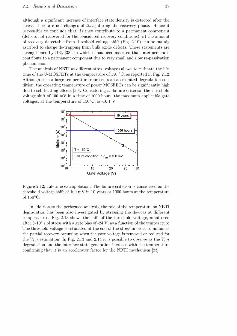
2.4. Results and Discussion 37
although a significant increase of interface state density is detected after thestress, there are not changes of ∆Dit during the recovery phase. Hence itis possible to conclude that: i) they contribute to a permanent component(defects not recovered for the considered recovery conditions); ii) the amountof recovery detectable from threshold voltage shift (Fig. 2.10) can be mainlyascribed to charge de-trapping from bulk oxide defects. These statements arestrengthened by [13], [38], in which it has been asserted that interface trapscontribute to a permanent component due to very small and slow re-passivationphenomenon.
The analysis of NBTI at different stress voltages allows to estimate the life-time of the U-MOSFETs at the temperature of 150 ◦C, as reported in Fig. 2.12.Although such a large temperature represents an accelerated degradation con-dition, the operating temperature of power MOSFETs can be significantly highdue to self-heating effects [39]. Considering as failure criterion the thresholdvoltage shift of 100 mV in a time of 1000 hours, the maximum applicable gatevoltages, at the temperature of 150◦C, is -16.1 V.
10 15 20 25 30102
103
104
105
106
107
108
109
1000 hours
lifet
ime
(s)
Gate Voltage (V)
10 years
Failure condition: VTH = 100 mV
T = 150°C
Figure 2.12: Lifetime extrapolation. The failure criterion is considered as thethreshold voltage shift of 100 mV in 10 years or 1000 hours at the temperatureof 150◦C.
In addition to the performed analysis, the role of the temperature on NBTIdegradation has been also investigated by stressing the devices at differenttemperatures. Fig. 2.13 shows the shift of the threshold voltage, monitoredafter 3 ·104 s of stress with a gate bias of -24 V, as a function of the temperature.The threshold voltage is estimated at the end of the stress in order to minimizethe partial recovery occurring when the gate voltage is removed or reduced forthe VTH estimation. In Fig. 2.13 and 2.14 it is possible to observe as the VTHdegradation and the interface state generation increase with the temperatureconfirming that it is an accelerator factor for the NBTI mechanism [23].
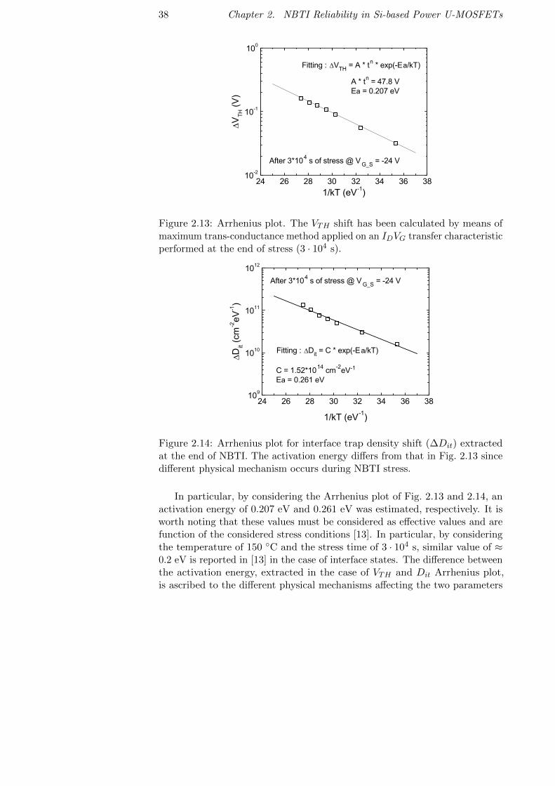
38 Chapter 2. NBTI Reliability in Si-based Power U-MOSFETs
24 26 28 30 32 34 36 3810-2
10-1
100
V TH (V
)
1/kT (eV-1)
After 3*104 s of stress @ V G_S = -24 V
Fitting : VTH = A * tn * exp(-Ea/kT)
A * tn = 47.8 VEa = 0.207 eV
Figure 2.13: Arrhenius plot. The VTH shift has been calculated by means ofmaximum trans-conductance method applied on an IDVG transfer characteristicperformed at the end of stress (3 · 104 s).
24 26 28 30 32 34 36 38109
1010
1011
1012
Dit (c
m-2eV
-1)
1/kT (eV-1)
Fitting : Dit = C * exp(-Ea/kT)
After 3*104 s of stress @ V G_S = -24 V
C = 1.52*1014 cm-2eV-1
Ea = 0.261 eV
Figure 2.14: Arrhenius plot for interface trap density shift (∆Dit) extractedat the end of NBTI. The activation energy differs from that in Fig. 2.13 sincedifferent physical mechanism occurs during NBTI stress.
In particular, by considering the Arrhenius plot of Fig. 2.13 and 2.14, anactivation energy of 0.207 eV and 0.261 eV was estimated, respectively. It isworth noting that these values must be considered as effective values and arefunction of the considered stress conditions [13]. In particular, by consideringthe temperature of 150 ◦C and the stress time of 3 · 104 s, similar value of ≈0.2 eV is reported in [13] in the case of interface states. The difference betweenthe activation energy, extracted in the case of VTH and Dit Arrhenius plot,is ascribed to the different physical mechanisms affecting the two parameters

2.4. Results and Discussion 39
during NBTI stress [13]. Moreover, it is worth noting that the activation energyextracted from ∆VTH is the result of the combined effect of oxide and interfacetrapped charge.
In Fig. 2.15, the threshold voltage recovery at different temperatures isshown. Since the stress and recovery phase are carried out at the sametemperature, the initial value of ∆VTH increases as long as the temperaturerises (as already discussed in Fig. 2.13). Moreover, in Fig. 2.15 it can beobserved that by increasing the temperature a faster recovery of VTH occurs,meaning that, as reported also in the case of CMOS technology [40]-[42], thetemperature is an acceleration factor also for the recovery mechanism.
10-2 10-1 100 101 102 103 104 105
4x10⁻²
8x10⁻²
1,2x10⁻¹
1,6x10⁻¹
V TH (V
)
Recovery Time (s)
T = 150 °C T = 140 °C T = 130 °CT = 120 °CT = 110 °C
T = 85 °C
T = 55 °C
After 3*104 s of stress @ V G_S = -24 V
VG_R = 0 V
Figure 2.15: Threshold voltage recovery for different temperatures after 3 · 104
s of stress at VG = -24 V. The same temperature is adopted during the stressand recovery phases. By increasing the temperature a faster recovery occurs,meaning that the temperature is an accelerator factor also for de-trappingmechanism.
Recovery dynamics, analyzed for different recovery gate voltages (VG R),are shown in Fig. 2.16. As it is possible to note, the recovery phase is VG R
dependent. In particular, we observe that: i) in the case of VG R = -2.25 V(VG R ≈ VTH after stress) the VTH recovery is negligible; ii) decreasing |VG R|,hence moving from VTH to the flat band voltage (VFB), a larger recoveryoccurs; iii) for VG R ranging from -0.25 V to 0 V no additional recovery isobserved. The gate voltage dependence is explained by the energy distributionof traps. In fact, traps having energy above the channel potential (Fermilevel at SiO2/Si interface) are filled with holes and are not discharged duringrecovery phase. On the other hand, traps below the channel potential aredischarged, leading to a recovery of VTH .

40 Chapter 2. NBTI Reliability in Si-based Power U-MOSFETs
100 101 102 103 104 105
6x10⁻²
9x10⁻²
1,2x10⁻¹
1,5x10⁻¹
1,8x10⁻¹
VG_R = - 2.25 V VG_R = - 2 V VG_R = - 1.5 V VG_R = - 1 V VG_R = - 0.5 V VG_R = - 0.25 V VG_R = 0 V
V TH (V
)
Recovery Time (s)
After 3*104 s of stress @ V G_S = -24 V
T = 150 °C
Figure 2.16: VTH recovery for different recovery biases. With VG R = -2.25V a negligible recovery is shown; moving the gate bias down to -0.25 V alarger recovery occurs. A further decrease of the gate voltage does not leadto additional recovery. Therefore, the traps involved in the recovery have anenergy confined within the band-gap of the silicon.
Therefore, TCAD numerical simulations, aimed at evaluating the channelpotential (Fermi level) and hence the oxide traps level, were implemented [24].A calibration of the simulated structure was performed in order to reproducethe characteristics of the real device. The flat band voltage, due to gatedoping and to the existing defects in fresh conditions, was taken into accountby properly setting the work function difference between gate electrode andthe semiconductor. Moreover, since the channel potential depends on thetrapped charge density (∆NOT ) after the stress phase, ∆NOT was estimatedby considering the experimental threshold voltage shift (∆VTH) as:
∆NOT =COX∆VTH
q(2.3)
where COX and q are the oxide capacitance for unit of area and the elementarycharge, respectively. Finally, the value calculated with Eq. 2.3 was accountedfor in the simulation.
The calculated band diagrams corresponding to the border conditions, i.e.start and end of recovery phase with VG R = -2.25 V and -0.25 V, respectively,at T = 150 ◦C, are reported in Fig. 2.17 and 2.18, respectively. According tothe discussion of Fig. 2.16, it can be asserted that the oxide traps involved inthe recovery mechanism have an energy confined between 0.22 eV and 0.84 eVfrom silicon valence band.

2.4. Results and Discussion 41
0,0 0,1 0,2
-5
0
5
EV
(eV)
(um)
Oxide Semiconductor
EC
Stress @ VG_S = -24 V ; T = 150 °C ; 3*10 4 s
Start of the RecoveryVG_R = -2.25 V
NOT = 8.08 * 1010 cm-2
EF - EV = 0.22 eV
oxide trapped holes
Figure 2.17: Band diagram at the start of recovery with an applied gate voltageof -2.25 V and a trap density, calculated with Eq. 2.3, of 8.08 ·1010 cm−2. Withthis gate bias all the charge, trapped during the stress, stays trapped into theoxide.
0,0 0,1 0,2
-5
0
5
oxidedetrapped holes
EV
(eV)
(um)
EC
Stress @ VG_S = -24 V ; T = 150 °C ; 3*10 4 s
End of the Recovery (6*10 4 s)VG_R = -0.25 V
NOT = 4.41 * 1010 cm-2
EF - EV = 0.84 eV
oxide trapped holes
Figure 2.18: Band diagram at the end of recovery (6 · 104 s) with an appliedgate voltage of -0.25 V and a trap density, calculated with Eq. 2.3, of 4.41 ·1010
cm−2. Traps with an energy level between 0.22 and 0.84 eV from silicon valenceband have been involved in the de-trapping process.
By combining the energy levels extracted with numerical simulations andthe experimental ∆NOT values calculated with Eq. 2.3, the energy distributionof the oxide charge de-trapping are reported in Fig. 2.19 and 2.20. Decreasing|VG R|, hence moving from VTH to VFB, a higher number of filled oxide trapslocated down below the Fermi level and a larger de-trapping charge occurs tillVG R reaches – 0.025 V (EF − EV = 0.84eV ) (Fig. 2.19). Moreover, a large

42 Chapter 2. NBTI Reliability in Si-based Power U-MOSFETs
part of these traps seems to be positioned close to conduction and valenceband of the semiconductor at the Si/SiO2 interface, since, from Fig. 2.20,it is possible to observe that the de-trapping charge concentration is highercompared to that occurring at the mid bandgap.
0,0 0,2 0,4 0,6 0,8 1,00
1
2
3
4
After 6*104 s of recovery After 104 s of recovery
NO
T_D
etra
p x10
10 (c
m-2)
EF-EV (eV)
Stressed @ VG_S = -24 V ; t = 3*10 4 sT = 150 °C
Negligible
Saturation
Figure 2.19: De-trapped oxide charge versus energy level after 104 s and atthe end of the recovery phase. A saturation of the charge de-trapping at 0.84eV from VB occurs, meaning that during the stress all the traps with higherenergy have been filled.
0,2 0,3 0,4 0,5 0,5 0,6 0,7 0,8 0,9
2
4
6
8
10
12
After 6*104 s of recovery After 104 s of recovery
NO
T_D
etra
p /E
x1010
(cm
-2eV
-1)
EF-EV (eV)
Stressed @ VG_S = -24 V ; t = 3*10 4 sT = 150 °C
Figure 2.20: De-trapped oxide charge density variation versus energy level.Higher de-trapping charge variation occurs near the valence and conductionband with respect to mid-gap of the silicon.
The oxide trap depth was estimated by using the tunneling time constantmodel. By considering a small oxide field, oxide charge can escape via a

2.4. Results and Discussion 43
trapezoidal barrier tunneling and, by assuming a single trap energy (ET ), thede-trapping time is given by [43]-[46]
τ = τ0 · exp(
2 ·√
2 ·m∗ · ET~2
· x)
(2.4)
where τ0, m∗, ET , ~2, and x are the time constant, charge tunneling effective
mass, trap energy level from SiO2 valence band, Dirac constant, and distanceof the trap from the Si/SiO2 interface, respectively.
In order to calculate the oxide trap distance (x) from SiO2/Si interface,the experimental dynamics of VTH recovery, shown in Fig. 2.21, has beenmodeled as the superposition of four first-order transients:
∆VTH = A·exp(− t
τ1
)+B ·exp
(− t
τ2
)+C ·exp
(− t
τ3
)+D ·exp
(− t
τ4
)(2.5)
with fitting parameters A, B, C, D = 8.09, 18.78, 25, 97.3 mV and τ1, τ2, τ3,τ4 = 18, 340, 6500, 320000 seconds, respectively.
0 1 2 3 4 5 6
0,08
0,10
0,12
0,14
0,16
V TH (V
)
Recovery Time x10 4 (s)
Experimental result Fitting
Maximum fitting error ± 1.5%
Recovery @ VG_R = 0 V and T = 150 °C
Figure 2.21: Experimental (markers) and modeled (line), with (3), thresholdvoltage shift versus recovery time for VG = 0 V and T = 150 ◦C.
The different de-trapping time constants suggest different depths of theoxide traps. By considering the lowest and the highest time constant in theenergy range of (0.22 - 0.84) eV, the possible physical locations of the traps,extracted with Eq. 2.4 are determined and reported in Fig. 2.22. As a result,we found a range of (2.24 - 3.04) nm distant from SiO2/Si interface, which isin agreement with [47] asserting that oxide traps are located within 6 nm fromSiO2/Si interface.
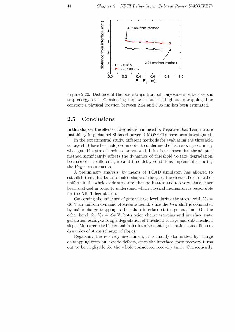
44 Chapter 2. NBTI Reliability in Si-based Power U-MOSFETs
0,0 0,2 0,4 0,6 0,8 1,00
1
2
3
4
5
2.24 nm from interface
dist
ance
from
inte
rface
(nm
)
ET - EV (eV)
= 18 s = 320000 s
3.05 nm from interface
Figure 2.22: Distance of the oxide traps from silicon/oxide interface versustrap energy level. Considering the lowest and the highest de-trapping timeconstant a physical location between 2.24 and 3.05 nm has been estimated.
2.5 Conclusions
In this chapter the effects of degradation induced by Negative Bias TemperatureInstability in p-channel Si-based power U-MOSFETs have been investigated.
In the experimental study, different methods for evaluating the thresholdvoltage shift have been adopted in order to underline the fast recovery occurringwhen gate-bias stress is reduced or removed. It has been shown that the adoptedmethod significantly affects the dynamics of threshold voltage degradation,because of the different gate and time delay conditions implemented duringthe VTH measurements.
A preliminary analysis, by means of TCAD simulator, has allowed toestablish that, thanks to rounded shape of the gate, the electric field is ratheruniform in the whole oxide structure, then both stress and recovery phases havebeen analyzed in order to understand which physical mechanism is responsiblefor the NBTI degradation.
Concerning the influence of gate voltage level during the stress, with VG =-16 V an uniform dynamic of stress is found, since the VTH shift is dominatedby oxide charge trapping rather than interface states generation. On theother hand, for VG = -24 V, both oxide charge trapping and interface stategeneration occur, causing a degradation of threshold voltage and sub-thresholdslope. Moreover, the higher and faster interface states generation cause differentdynamics of stress (change of slope).
Regarding the recovery mechanism, it is mainly dominated by chargede-trapping from bulk oxide defects, since the interface state recovery turnsout to be negligible for the whole considered recovery time. Consequently,

2.5. Conclusions 45
a combined measurement/simulation methodology has been implemented inorder to evaluate the spatial and energy oxide trap distribution.
In particular, by performing an experimental study on the recovery mech-anisms at different bias conditions, it has been found that the oxide trapsinvolved during NBTI stress have an energy confined in the silicon bandgap.Afterwards, by accounting for the experimental results in TCAD simulations,an oxide trap distribution with an energy level confined between 0.22 eV and0.84 eV from silicon valence band has been estimated.
Finally, by adopting the tunneling constant model, it has been calculatedthat the distance of oxide traps from SiO2/Si interface may range between2.24 and 3.04 nm.
References
[1] D. K. Schroeder, ”Negative bias temperature instability: What do weunderstand?,” Microelectronics Reliability, Vol. 47, No. 6, pp. 841-852,2007.
[2] N. Stojadinovic, I. Manic, V. Davidovic, D. Dankovic, S. Djoric-Velikovic,S. Golubovic, S. Dimitrijev, “Electrical stressing effects in commercialpower VDMOSFETs,” IEEE Proc.-Circuits Devices Syst., Vol. 153, No. 3,pp. 281-288, 2006.
[3] R. Green, A. Lelis, and D. Habersat, “Application of reliability test stan-dards to SiC power MOSFETs,” IEEE International Reliability PhysicsSymposium, pp. 756-764, Monterey, CA, USA, 2011.
[4] F. J. Grunthaner and J. Maserjian, “Experimental observations of thechemistry of the SiO2/Si interface,” IEEE Transactions on Nuclear Science,Vol. 24, No. 6, pp. 2108-2112, 1977.
[5] Y. Nissan-Cohen and T. Gorczyca, “The effect of hydrogen on trap gener-ation, positive charge trapping, and time-dependent dielectric breakdownof gate oxides,” IEEE Electron Device Letters, Vol. 9, No. 6, pp. 287-289,1988.
[6] M. A. Alam, S. Mahapatra, “A comprehensive model of PMOS NBTIdegradation,” Microelectronics Reliability, Vol. 45, No. 6, pp. 71-81, 2005.
[7] K. O. Jeppson, C. M. Svensson, ”Negative bias stress of MOS devices athigh electric fields and degradation of MNOS devices,” Journal of AppliedPhysics, Vol. 48, 2004.
[8] S. Ogawa, N. Shiono, ”Generalized diffusion–reaction model for the low-field charge build up instability at the Si–SiO2 interface,” Physical ReviewB, Vol. 51, No. 7, 1995.
[9] T. Grasser, B. Kaczer, W. Goes, T. Aichinger, P. Hehenberger, and M.Nelhiebel, “A two stage model for negative bias temperature instability,”IEEE International Reliability Physics Symposium, pp. 33-44, Montreal,QC, 2009.
46

References 47
[10] V. Huard, “Two independent components modeling for negative bias tem-perature instability”, IEEE, International Reliability Physics Symposium,”IEEE International Reliability Physics Symposium, pp. 33-42, Anaheim,CA, 2010.
[11] ] S. Mahapatra, K. Ahmed, D. Varghese, A. E. Islam, G. Gupta, L. Madhav,D. Saha, and M. A. Alam, “On the physical mechanism of NBTI in siliconoxynitride p-MOSFETs: Can differences in insulator processing conditionsresolve the interface trap generation versus hole trapping controversy?,”IEEE International Reliability Physics Symposium, pp. 1-9, Phoenix, AZ,2007.
[12] J. H. Stathis and S. Zafar, “The negative bias temperature instability inMOS devices: A review,” Microelectronics Reliability, Vol. 46, No. 2-4, pp.270-286, 2006.
[13] V. Huard, M. Denais, C. Parthasarathy, “NBTI degradation: From physi-cal mechanisms to modeling,” Microelectronics Reliability, Vol. 46, No. 1,pp. 1-23, 2006.
[14] D. Dankovic, N. Stojadinovic, Z. Prijic, I. Manic, and A. Prijic, “Recov-erable and permanent components of VT shift in pulsed NBT stressedp-channel power VDMOSFETs,” IEEE Internation Conference on Micro-electronics, pp. 297-300, Belgrade, 2014.
[15] N. A. Othman, N. M. Karim, M. Sufyan, and N. Soin, “Impact of pro-cessing parameters on low-voltage power MOSFET threshold voltageconsidering defect generation,” IEEE Regional Symposium on Micro andNanoelectronics, pp. 231-234, Langkawi, 2013.
[16] N. Stojadinovic, I. Manic, V. Davidovic, D. Dankovic, S. Doric-Veljkovic,S. Golubovic, S. Dimitrijev, ”Effects of gate bias stressing in power VD-MOSFETs,” Serbian Journal of Electrical Engineering, Vol. 1, No. 1, pp.89-101, 2003.
[17] T. Aoki, Y. Tsuzuki, S. Miura, Y. Okabe, M. Suzuki and A. Kuroyanagi,“High performance and reliability trench gate power MOSFET with par-tially thick gate oxide film structure (PTOx-TMOS),” IEEE InternationalSymposium on Power Semiconductor Devices and IC’s, pp. 1-4, Naples,Italy, 2006.
[18] R. Giahn-Horng Lee, Jen-Shien Su, and Steve S. Chung, “A new methodfor characterizing the spatial distributions of interface states and oxide-trapped charges in LDD n-MOSFETs,” IEEE Transaction on ElectronDevices, Vol. 43, No. 1, pp. 81-89, 1996.

48 References
[19] D. Veksler, G. Bersuker, A. Koudymov, and M. Liehr, “Analysis of charge-pumping data for identification of dielectric defects,” IEEE Transactionon Electron Devices, Vol. 60, No. 5, pp. 1514-1522, 2013.
[20] B. J. Baliga, “Fundamentals of Power Semiconductor Devices,” Springer,2008, ISBN: 978-0-387-47314-7.
[21] R. S. Saxena and M. J. Kumar, “Trench gate power MOSFET: Recentadvances and innovations,” Advances in Microelectronics and Photonics,Chapter 1, pp. 1-23, New York, USA, 2012.
[22] H. Shah, S. Oknaian, E. Persson and R. Huang, “From planar to trench –evaluation of ruggedness across various generations of power MOSFETsand implications on in-circuit performance,” IEEE Applied Power Elec-tronics Conference and Exposition, pp. 485-490, Fort Worth, Texas, USA,2011.
[23] J. Qin, J. B. Bernstein, “Non-arrhenius temperature acceleration andstress-dependent voltage acceleration for semiconductor device involvingmultiple failure mechanisms,” IEEE International Integrated ReliabilityWorkshop, pp. 93-97, South Lake Tahoe, CA, 2006.
[24] Sentaurus-Device U.G. v. J-2014.09, Synopsys Inc., 2014.
[25] L. Tsetseris, X. J. Zhou, D. M. Fleetwood, and R. D. Schrimpf, “Physicalmechanisms of the negative-bias temperature instability,” Applied PhysicsLetters, Vol. 86, 142103, 2005.
[26] D. K. Schroder and J. A. Babcock, “Negative bias temperature instability:Road to cross in deep submicron silicon semiconductor manufacturing,”Journal of Applied Physics, Vol. 94, No. 1, pp. 1-18, 2003.
[27] T. Grasser, P.-J. Wagner, P. Hehenberger, W. Goes, and B. Kaczer, “ Arigorous study of measurement techniques for negative bias temperatureinstability,” IEEE Transaction on Device and Materials Reliability, Vol. 8,No. 3, pp. 526-535, 2008.
[28] D. K. Schroder, “Semiconductor material and device characterization,”Third Edition, Arizona State University Tempe, AZ, 2006.
[29] B. Kaczer, V. Arkhipov, R. Degraeve, N. Collaert, G. Groeseneken, andM. Goodwin, “Disorder-controlled-kinetics model for negative bias tem-perature instability and its experimental verification,” IEEE InternationalReliability Physics Symposium, pp. 381-387, San Joe, CA, USA, 2005.
[30] S. Rangan, N. Mielke, Everett C.C. Yeh, “Universal recovery behaviorof negative bias temperature instability,” IEEE International ElectronDevices Meeting, pp. 14.3.1-14.3.4, Washington, DC, USA, 2003.

References 49
[31] R. W. Herfst, J. Schmitz, and A. J. Scholten, “Simultaneous extraction ofthreshold voltage and mobility degradation from on-the-fly NBTI mea-surements,” IEEE Internation Reliability Physics Symposium, pp. 6.1-6.4,Monterey, CA, USA, 2011.
[32] H. Reisinger, O. Blank, W. Muhlhoff, W. Gustin, and C. Schlunder,“Analysis of NBTI degradation-and recovery-behavior based on ultra fastVT-measurements,” IEEE International Reliability Physics Symposium,pp. 448-453, San Jose, CA, USA, 2006.
[33] C. Schlunder, W. Heinrigs, W. Gustin, and H. Reisinger, “On the impactof the NBTI recovery phenomenon on lifetime prediction of modern p-MOSFETs,” IEEE International Integrated Reliability Workshop, pp. 1-4,South Lake Tahoe, CA, USA, 2006.
[34] V. Reddy, J. Carulli, A. Krishnan, W. Bosch, and B. Burgess, “Impact ofnegative bias temperature instability on product parametric drift,” IEEEInternational Test Conference, pp. 148-155, 2004.
[35] C. Shen, M. F. Li, C. E. Foo, T. Yang, D. M. Huang, A. Yap, G. S.Samudra, and Y. C. Yeo, “Characterization and physical origin of fastVTH transient in NBTI of pMOSFETs with SiON dielectric,” IEEEInternational Electron Devices Meeting, pp. 1-4, San Francisco, CA, USA,2006.
[36] E. N. Kumar, V. D. Maheta, S. Purawat, A. E. Islam, C. Olsen, K.Ahmed, M. Alam, and S. Mahapatra, “Material dependence of NBTIphysical mechanism in silicon oxynitride (SiON) p-MOSFETs: A compre-hensive study by ultrafast on-the-fly (UF-OTF IDLIN technique,” IEEEInternational Electron Devices Meeting, pp. 809-812, Washington, DC,2007.
[37] N. Stojadinovic, D. Dankovic, S. Djoric-Veljkovic, V. Davidovic, I. Manic,S. Golubovic, “Negative bias temperature instability mechanisms in p-channel power VDMOSFETs,” Microelectronics Reliability, Vol. 45, No.9-11, pp.1343-1348, 2005.
[38] Y. Yonamoto, “Similarity and difference in temperature dependent recov-ery of HCS and NBTI,” IEEE International Reliability Physics Symposium,pp. XT.1.1-XT.1.6, Waikoloa, HI, 2014.
[39] P. Magnone, C, Fiegna, G. Greco, G. Bazzano, S. Rinaudo, E. Sangiorgi”Numerical simulation and modeling of thermal transient in silicon powerdevices,” Solid-State Electronics, Vol. 88, pp. 69-72, 2013.
[40] Y. Yonamoto, “Recovery behavior in negative bias temperature instability,”Microelectronics Reliability, Vol. 54. No. 3, pp. 520-528, 2014.

50 References
[41] A. Katsetos, “Negative bias temperature instability (NBTI) recovery withbake,” Microelectronics Reliability, Vol. 48, No. 10, pp. 1655-1659, 2008.
[42] T. Aichinger, M. Nelhiebel, T. Grasser, “Refined NBTI characterization ofarbitrarily stressed PMOS devices at ultra-low and unique temperatures,”Microelectronics Reliability, Vol. 53, No. 7, pp. 937-946, 2013.
[43] H. Lakhdari, D. Vuillaume, and J. C. Bourgoin, “Spatial and energeticdistribution of Si-SiO2 near-interface states,” Physical Review B, Vol. 38,No. 18, pp. 13124-13132, 1988.
[44] I. Lundstrom and C. Svensson, “Tunneling to traps in insulators,” Journalof Applied Physics, Vol. 43, No. 12, pp. 5045-5047, 1972.
[45] C. J. Kang, S. Lee, Y. Kuk, “Depth-dependent detrapping dynamics ofelectrons in SiO2,” Journal of the Korean Physical Society, Vol. 40, No.3, pp. 472-475, 2002.
[46] C. T. Chan, H. C. Ma, C. J. Tang, and T. Wang, “Investigation of post-NBTI stress recovery in pMOSFETs by direct measurement of single oxidecharge de-trapping,” Symposium on VLSI Technology, pp. 90-91, 2005.
[47] Q. D. M. Khosru, N. Yasuda, K. Taniguchi, and C. Hamaguchi, “Genera-tion and relaxation phenomena of positive charge and interface trap ina metal-oxide-semiconductor structure,” Journal of Applied Physics, Vol.77, No. 9, pp. 4494-4503, 1995.

Chapter 3
Modeling Self-Heating Effects inGaN-based HEMTs
3.1 Introduction and State of the Art
GaN-based transistors, as largely introduced in chapter 1, thanks to the intrinsicproperties of the adopted materials, represent today a potential technology forswitching power applications [1]-[3]. However, high performance is not enough,as a high level of reliability must be guaranteed under heavy-duty operation.For this reason, different works about heterostructures reliability have beenfocused on the charges trapping/de-trapping mechanisms [4]-[7].
However, since a power transistor is subject to high temperatures dur-ing its normal operation, self-heating effects play an important role in theunderstanding of the device performance limitations.
Several studies reported in the literature [8]-[13] have pointed out as thecontribution of the thermal boundary resistance (TBR), introduced by thetransition layer (or nucleation layer) between GaN-buffer and Si- or SiC-substrate in order to reduce the lattice constants mismatch, is fundamentalfor modeling the self-heating effects in the devices. Indeed, Sarua et al. [9]have experimentally proposed a model, based on GaN-on-SiC devices, ableto describe the temperature dependence of the TBR emphasizing how itscontribution becomes more and more important with the temperature increase.A similar study has been performed by Schwitter et al. [8] for AlGaN/GaNdevices grown on silicon substrate.
In this chapter, a simulation study of self-heating effects has been performedin order to understand the performance limitations, under both static anddynamic operation modes. To this purpose, a physical model able to accountfor the realistic temperature dependence of the equivalent thermal boundaryresistance ascribed to transition layer, has been implemented for both GaN-on-SiC and GaN-on-Si technologies.
51

52 Chapter 3. Modeling Self-Heating Effects in GaN-based HEMTs
3.2 Thermal Model Implementation
By considering for each material involved in the transition layer the simulator’sdefault models for the thermal conductivity, the total transition layer thermalresistance results underestimated because its temperature-dependence andthe interface impact between two different materials are not accounted for.In particular, in the case of Sentaurus TCAD the thermal conductivity ofsome materials, such as those AlN-based, is still reproduced as a temperature-independent constant [14]. Moreover, since materials with significant latticemismatch and difference in thermal expansion coefficients are adopted, theimpact of the interfacial thermal resistance could be dominant with respect tothat of the bulk material or, at least, contributes to increase the total thermalresistance value.
Therefore, a specific Physical Model Interface (PMI) has been implemented,by means of C++ subroutines, in TCAD Sentaurus simulator in order toproperly set the thermal boundary resistance (TBR) between GaN channel(layer) and substrate. This model is self-consistently solved with the DriftDiffusion model.
According to literature results based on an experimental characterization[8], [9], the implemented temperature-dependent thermal conductivity (k(T))of the transition layer is modeled as:
k(T ) = k0 ·( TT0
)α(3.1)
where k0 is the thermal conductivity at T0 = 300K and α is the power lawcoefficient. Both depend on the kind of substrate (Si or SiC in this work)and thus on the types of materials and their respective thickness adopted forthe transition layer. Therefore, their values will be specified further in thefollowing sections.
3.3 GaN-on-SiC Structure
3.3.1 Device Structure and Physical Models
Fig. 3.1 shows the simulated AlGaN/GaN structure. It was defined con-sidering typical geometric characteristics and material parameters proposedin experimental works reported in the literature (e.g. [5]). The structurefeatures a stack of SiN/AlGaN/GaN/Oxide/SiC layers with thickness of50nm/29nm/1.5µm/10nm/100µm, respectively. The aluminum concentrationin AlGaN barrier, which plays an important role in device operation throughthe piezoelectric charge induced by mechanical stress, is set to 35 %, represent-ing a typical value for state-of-art devices [5]. Drain and source electrodes aremodeled as ohmic contacts with length LS = LD = 0.5 µm, whereas the 0.7

3.3. GaN-on-SiC Structure 53
µm long gate electrode is modeled as a Schottky contact, with 1.1 eV barrierheight, representing a typical measured value for realistic devices [15], [16].The drain- and source-to channel access regions feature lengths of LSG = 0.7µm and LGD = 2 µm, respectively. Finally, a device pitch (LDEV PITCH) of4.4 µm was assumed.
Figure 3.1: Simulated AlGaN/GaN HEMT structure. To allow a self-heatingstudy, a thermode contact, fixed at the temperature of 300 K, is introduced atthe bottom of the SiC substrate. Figure not in scale.
Donor-traps have been added at the SiN/AlGaN interface. Their intro-duction is important not only for studying the dispersion effects due to de-trapping/trapping phenomena, but also because the traps occupancy is requiredto set an adequate channel electrical conductivity, since the combined effect ofthe interface trapped- and polarization-charge is indispensable for filling thechannel of electrons.
Moreover, since Meneghesso et al. [5] have shown that surface donor-trapsare responsible for a drain current dispersion effect, a single trap energy level of0.5 eV from valence band has been adopted in order to have a finite transienttime, required by traps to respond to an external voltage signal, similar to thatobtained in [5] during drain-lag measurements.
The device features an oxide nucleation layer that significantly affectsself-heating effects due to motivations discussed in section 3.2. This effect hasbeen modeled in [9] by defining an equivalent thermal boundary resistance(TBR) interposed between the GaN buffer and the SiC substrate. Sarua etal. [9] experimentally investigated the temperature dependence of the TBR inAlGaN/GaN devices proposing a model able to reproduce the experimentalresults. It is worth noting that, as discussed in section 1.4, the nucleation layeris not usually made of oxide. However, since the aim of this work was the studyof its thermal behavior instead of the electrical one, the kind of the adoptedmaterial is not important once the thermal conductivity is properly calibrated.
In this study, Sarua’s model has been implemented and included in the

54 Chapter 3. Modeling Self-Heating Effects in GaN-based HEMTs
simulation tool through the device simulator’s model interface in order torealistically model self-heating effects. In particular, by referring to modelreported in Eq. 3.1, k0 = 2.78 W/m·K and α = −2.76 have been adoptedfor modeling the temperature-dependent thermal conductivity of the overalltransition/nucleation layer, whereas simulator’s default models and parametershave been used for AlGaN, GaN and SiC layers [14].
300 350 400 450 500 550 600 6500
2
4
6
8
10
12
Simulation results by Sentaurus TCAD Experimental results by A. Sarua [9]Power law by A. Sarua [9]
TBR
X10
- 4 (c
m2 K
W -1
)
Temperature (K)
Figure 3.2: Calibration of the TBR by means of experimental results [9]. APMI model has been implemented in the TCAD device simulator in order toaccount for the temperature dependence of the thermal conductivity.
0,1 1 10 100
300
600
900
1200
Tem
pera
ture
(K)
Position along the device ( m)
P = 3.78 W/mm P = 2.96 W/mm P = 1.97 W/mm P = 0.99 W/mm
GaN buffer SiC substrateTBR
Figure 3.3: Thermal distribution along the device (vertical direction) fordifferent electric powers. By increasing the temperature, the thermal boundaryresistance (TBR) contribution plays an important role in the temperaturebehavior of device.

3.3. GaN-on-SiC Structure 55
The implementation of the model for the thermal conductivity of thenucleation layer is validated in Fig. 3.2 by comparison with the experimentaldata for TBR reported by Sarua et al. in [9] and with the empirical power lawproposed in the same paper. By considering Fig. 3.3, it is worth noting howthe TBR becomes more and more important as the power dissipation increases,emphasizing the importance of the developed model for a realistic simulation.
3.3.2 Simulation Results and Discussion
In order to analyze the effect of mutual heating among adjacent devices,structures with different pitch (LSTR PITCH) have been simulated.
0,0 2,5 5,0 7,5 10,0 12,5 15,00,0
0,2
0,4
0,6
0,8
1,0
Dra
in C
urre
nt (A
/mm
)
Drain Voltage (V)
604.4 24.4 204.4 10.4 64.4 4.4
LSTR_PITCH ( m)
TTHERMODE = 300 KETRAPS = 0.5 eV from Valence Band
Figure 3.4: Simulated static IDVD characteristics evaluated on devices withdifferent pitch. By increasing the pitch, the current increases because of thelower power density, leading to a reduction of the temperature in the channeland hence to an improvement of electron mobility.
Fig. 3.4 shows the simulated static IDVD characteristics for structuresfeaturing different LSTR PITCH values. By increasing LSTR PITCH , the mutualheating effect is reduced and a lower power density is dissipated. As result ahigher drain current is found.
In fact, according to Fig. 3.5, a channel temperature of 640 K and 335 Kis found in the case of structure pitch of 4.4 µm and 604.4 µm, respectively,leading to a corresponding electron mobility, averaged along the channel, of525 and 900 cm2V −1s−1, respectively.
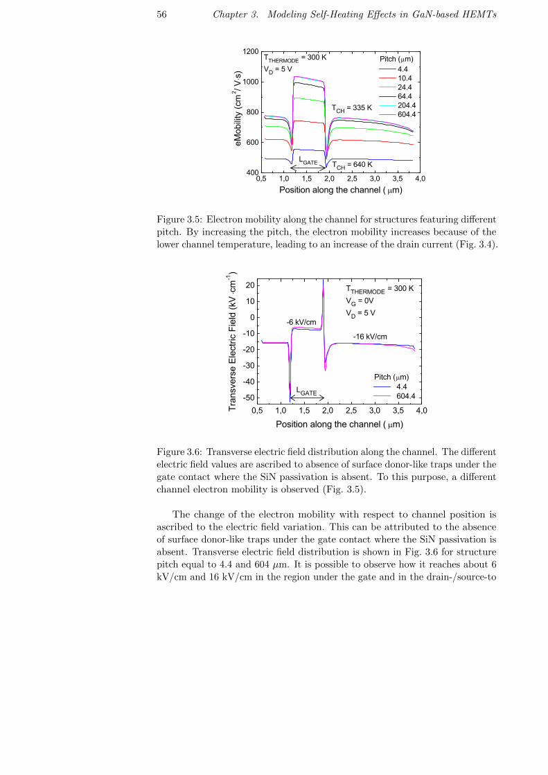
56 Chapter 3. Modeling Self-Heating Effects in GaN-based HEMTs
0,5 1,0 1,5 2,0 2,5 3,0 3,5 4,0400
600
800
1000
1200
TCH = 640 K
eMob
ility
(cm
2 / Vs)
Position along the channel ( m)
4.4 10.4 24.4 64.4 204.4 604.4
Pitch ( m)
TCH = 335 K
TTHERMODE = 300 KVD = 5 V
LGATE
Figure 3.5: Electron mobility along the channel for structures featuring differentpitch. By increasing the pitch, the electron mobility increases because of thelower channel temperature, leading to an increase of the drain current (Fig. 3.4).
0,5 1,0 1,5 2,0 2,5 3,0 3,5 4,0-50
-40
-30
-20
-10
0
10
20
-16 kV/cm
Tran
sver
se E
lect
ric F
ield
(kV
cm-1
)
Position along the channel ( m)
4.4 604.4
Pitch ( m)
-6 kV/cm
LGATE
TTHERMODE = 300 KVG = 0VVD = 5 V
Figure 3.6: Transverse electric field distribution along the channel. The differentelectric field values are ascribed to absence of surface donor-like traps under thegate contact where the SiN passivation is absent. To this purpose, a differentchannel electron mobility is observed (Fig. 3.5).
The change of the electron mobility with respect to channel position isascribed to the electric field variation. This can be attributed to the absenceof surface donor-like traps under the gate contact where the SiN passivation isabsent. Transverse electric field distribution is shown in Fig. 3.6 for structurepitch equal to 4.4 and 604 µm. It is possible to observe how it reaches about 6kV/cm and 16 kV/cm in the region under the gate and in the drain-/source-to

3.3. GaN-on-SiC Structure 57
channel access regions, respectively. These results are consistent with thesignificant decrease of electron mobility in AlGaN/GaN, for electric field largerthan 5 kV/cm, reported in [17]. Therefore, the degradation of mobility alongthe channel can be ascribed to the large electric field values.
10-8 10-7 10-6 10-5 10-4 10-3 10-20,0
0,2
0,4
0,6
0,8
1,0
Dra
in C
urre
nt (A
/mm
)
Time (s)
604.4 24.4 204.4 10.4 64.4 4.4 4.4 isothermal
LSTR_PITCH (um)
ETRAPS = 0.5 eV from VB ; T THERMODE = 300 K
current overshoot
Figure 3.7: Drain-lag simulations for structures with different pitch. Thecurrent overshoot is linked to the transient of donor traps which is shorter butwider for higher temperatures.
10-8 10-7 10-6 10-5 10-4 10-3 10-22,31
2,32
2,33
2,34
2,35
2,36
2,37
2,38
2,39
Ioni
zed-
Don
or-tr
aps
x10
13 (c
m-2
)
Time (s)
4.4 isothermal
300
400
500
600
700
800
4.4 10.4 24.4
Max
imum
Tem
pera
ture
(K)
LSTR_PITCH ( m)
ETRAPS = 0.5 eV from VB
Figure 3.8: Ionized-donor-traps averaged over the whole SiN/AlGaN interface(left-axis), and maximum temperature in the channel (right-axis) as function ofthe time during drain-lag simulations (Fig. 3.7). While a single traps transientappears in the case of isothermal simulations, a second one is activated if, dueto self-heating, the temperature exceeds approximately 540 K.
The dynamic behavior during drain-lag simulations for VD switched between

58 Chapter 3. Modeling Self-Heating Effects in GaN-based HEMTs
0 and 10 V in 10 ns at VG = 0 V is reported in Fig. 3.7 for structures witha different pitch. The amplitude of the drain voltage sweep has been chosenaccording with experimental and simulation works present in literature (e.g.[18]), whereas the ramp rate (1 V/ns) has been settled in order to have thetrap transient starting after that drain voltage has reached the final level,allowing to monitor the whole traps transient. A drain current overshoot dueto donor-traps transient is observable. Fig. 3.8 reports the time evolution oftraps occupancy for devices with different pitch values. While a single transientappears in the case of isothermal simulations, a second one is activated if,due to self-heating, the temperature exceeds approximately 540 K. Indeed,for structure pitch larger than 10.4 µm the second transient does not occur(see also Fig. 3.7) since the increase of temperature, induced by self-heating,is limited. This suggests the presence of a trapping mechanism caused bytwo different source. The first one is electrical-related because noticeable alsoin the case of isothermal simulation (Fig. 3.7), whereas the second one isthermal-related (Fig. 3.8).
0,5 1,0 1,5 2,0 2,5 3,0 3,5 4,00,0
0,5
1,0
1,5
2,0
2,5
3,0
Ioni
zed-
Don
or-tr
aps
x10
13 (c
m-2)
Position along SiN/AlGaN interface ( m)
After transient Before transient
LSG LG L GD
ETRAPS = 0.5 eV from VB
Figure 3.9: Traps occupancy along the SiN/AlGaN interface. Highertrapping/de-trapping phenomena are observed in the region close to the draincontact.
Finally, Fig. 3.9 reports the spatial dependence of trapping/de-trappingphenomena, suggesting that drain current dispersion effects, is mainly relatedto traps located in the region close to the drain contact. It is worth notingthat the device structure does not have contact field-plates (see Fig. 3.1) andthe surface donor-like traps under the gate contact are not considered sinceSiN passivation, in this region, is absent.

3.4. GaN-on-Si Structure 59
3.4 GaN-on-Si Structure
Similar analyses have been performed for GaN-on-Silicon devices. In particular,a 100 µm thick silicon substrate has been considered in order to model theself-heating effect during the transistor operation mode.
The device features a transition layer, composed of aluminum nitride (AlN)and different layers of AlGaN with different aluminum contents, significantlyaffecting the self-heating effects due to low thermal conductivity.
As in the case of GaN-on-SiC devices, this effect has been discussed andmodeled, by means of experimental analysis reported in [8], in order to definean equivalent thermal boundary resistance (TBR) interposed between the GaNbuffer and the Si substrate. As a result, the device simulator’s model interface(PMI), implemented for devices with SiC substrate, has been optimized andcalibrated for Si-substrate according to [8].
Unlike the case of GaN-on-SiC, where the PMI has been implemented onlyfor the thermal resistance contribution of the transition layer, in the case ofsilicon substrate also the AlGaN barrier and GaN buffer contributions havebeen modeled by means of PMI because suggested in the experimental studyof GaN-on-Si HEMT [8].
Model parameters for given temperature ranges are provided in Table 3.1.
Material k0 (W/m ·K) α Temp.Range(K)
GaN 150.0 -1.42 300-800
AlGaN 25.0 -1.44 300-500
TBReff transition layer 32.74 -2.09 300-500
Table 3.1: Thermal parameters adopted in GaN, AlGaN and transition layer.The considered model is reported in Eq. 3.1, while the calibration of theparameters have been done according to [8].
As already mentioned, the transition layer features, in the case of silicon sub-strate, a stack of different materials (1.6 µm−Al21Ga79N/ 0.5 µm−Al40Ga60N/0.5 µm−Al76Ga24N/ 150 nm−AlN). However, from thermal point of view,in the simulation, the transition layer is considered as a homogeneous ma-terial, in which all the layers have the same parameters (TBReff transitionlayer reported in the Table 3.1). Moreover, the simulator’s default models fortemperature-dependent thermal conductivity have been used for the siliconsubstrate.
By considering Fig. 3.10, it is worth noting how the TBR contribution,associated to the overall transition layer, plays an important role in the temper-ature behavior of device, emphasizing the importance of the developed modelfor a realistic simulation. In fact, by considering the temperature distributionof Fig. 3.10, it is possible to note that an underestimated channel temperature

60 Chapter 3. Modeling Self-Heating Effects in GaN-based HEMTs
is evaluated when default Sentaurus models are considered for the tempera-ture dependence of the thermal conductivity related to the materials of thetransition layer.
0,1 1 10 100300
350
400
450
500
550
k(T) by reference [8] k(T) by Sentaurus
Tem
pera
ture
(K)
Position along the device ( m)
Si-substrate
Transition layer=TBR
VG = 0VVD = 10VID = 1.7 A/mm
Figure 3.10: Thermal distribution along the device (vertical direction). Thethermal boundary resistance (TBR) contribution, modeled by [8], plays animportant role in the temperature behavior of device. Moreover, a relevanttemperature distribution difference is observable with respect to the case ofdefault Sentaurus models.
0 2 4 6 8 10 12 140,0
0,5
1,0
1,5
2,0
Dra
in C
urre
nt (A
/mm
)
Drain Voltage (V)
isothermal self-heating
VG = 0 VTTHERMODE = 300 KLSTR_PITCH = 26 m
Figure 3.11: Simulated static IDVD characteristics. By considering the self-heating effect, a lower drain current is observed with respect to isothermal casedue to the higher channel temperature and hence to the mobility degradation.

3.5. Conclusions 61
Finally, the static output characteristics (IDVD) is shown in Fig. 3.11. Byaccounting for the self-heating effects in the simulations, higher temperaturesoccur in the device leading to a mobility degradation. As a result, a lowercurrent density is observed.
3.5 Conclusions
A physical model interface (PMI) accounting for the impact of the transitionlayer on the self-heating in GaN-based power transistors with silicon and siliconcarbide substrate has been implemented and applied to a simulation studyof the static and dynamic operation mode. It has been shown that, non-considering the TBR contribution, the device channel/junction temperaturecan be underestimated up to 25/30 %. Consequently, different trapping relateddegradation mechanisms may be not fully exploited causing an inaccuratedevice lifetime prediction.

References
[1] M.S. Shur, R. Gaska, A. Bykhovisky, “GaN-based electronic device,”Solid-State Electronics, Vol. 43, No. 8, pp. 1451-1458, 1999.
[2] N. Ikeda, Y. Niiyama, H. Kambayashi, Y. Sato, T. Nomura, S. Kato,and S. Yoshida, “GaN Power Transistors on Si Substrate for SwitchingApplications,” Proceedings of the IEEE, Vol. 98, No. 7, pp. 1151-1161,2010.
[3] M.S. Shur, “GaN based Transtistors for High Power Applications,” Solid-State Electronics, Vol. 42, No. 12, pp. 2131-2138, 1998.
[4] J.A. del Alamo, J. Joh, “GaN HEMT reliability,” Microelectronics Relia-bility, Vol. 49, No. 9-11, pp. 1200-1206, 2009.
[5] G. Meneghesso, G. Verzellesi, R. Pierobon, F. Rampazzo, A. Chini, U.K.Mishra, C. Canali, and E. Zanoni, “Surface-Related Drain Current Dis-persion Effects in AlGaN-GaN HEMTs,” IEEE Transaction on ElectronDevices, Vol. 51, No. 10, pp. 1554-1561, 2004.
[6] M. Faqir, G. Verzellesi, G. Meneghesso, E. Zanoni, and F. Fantini, “In-vestigation of High-Electric-Field Degradation Effects in AlGaN/GaNHEMTs,” IEEE Transaction on Electron Devices, Vol. 55, No. 7, pp.1592-1602, 2008.
[7] G. Meneghesso, M. Meneghini, D. Bisi, I. Rossetto, A. Cester, U.K. Mishra,and E. Zanoni, “Trapping phenomena in AlGaN/GaN HEMTs: a studybased on pulsed and transient measurements,” Semiconductor Science andTechnology, Vol.28, No. 7, pp. 1-8, 2013.
[8] B.K. Schwitter, A.E. Parker, S.J. Mahon, A.P. Fattorini, M.C. Heimlich,“Impact of Bias and Device Structure on Gate Junction Temperature inAlGaN/GaN-on-Si HEMT,” IEEE Transaction on Electron Devices, Vol.61, No. 5, pp. 1327-1334, 2014.
[9] A. Sarua, H. Ji, K.P. Hilton, D.J. Wallis, M.J. Uren, T. Martin, and M.Kuball, “Thermal Boundary Resistance Between GaN and Substrate in
62

References 63
AlGaN/GaN Electronic Devices,” IEEE Transaction on Electron Devices,Vol. 54, No. 12, pp. 3152-3158, 2010.
[10] J. Kuzmik, S. Bychikhin, D. Pogany, C. Gaquiere, E. Pichonat, and E.Morvan, “Investigation of the thermal boundary resistance at the III-nitride/substrate interface using optical methods,” Journal of AppliedPhysics, Vol. 101, No. 5, pp. 1-6, 2007.
[11] J. Cho, Y. Li, D. H. Altman, W. E. Hoke, M. Asheghi, and K. E. Goodson,“Temperature dependent thermal resistances at GaN-substrate interfacesin GaN composite substrates,” IEEE Compound Semiconductor IntegratedCircuit Symposium, pp. 1-4, 2012.
[12] A. Manoi, J. W. Pomeroy, N. Killat, and M. Kuball, “Benchmarking ofthermal boundary resistance in AlGaN/GaN HEMTs on SiC substrate:Implications of the nucleation layer microstructure,” IEEE Electron DeviceLetters, Vol. 31, No. 12, pp. 1395-1397, 2010.
[13] E. R. Heller and A. Crespo, “Electro-thermal modelling of multifingerAlGaN/GaN HEMT device operation including thermal substrate effects,”Microelectronics Reliability, Vol. 48, No. 45, pp. 45-50, 2008.
[14] Sentaurus-Device U.G. v. L-2016.03, Synopsys Inc., 2016.
[15] Z. Lin, W. Lu, J. Lee, D. Liu, J.S. Flynn, and G.R. Brandes, “Barrierheights of Schottky contacts on strained AlGaN/GaN heterostructures:Determination and effect of metal work functions,” Applied Physics Letter,Vol. 82, No. 24, pp. 4364-4366, 2003.
[16] A. F. M. Anwar, E. W. Faraclas, “Schottky barrier height in GaN/AlGaNheterostructures,” Solid-State Electronics, Vol. 50, No. 6, pp. 1041-1045,2006.
[17] L. Ardaravicius, A. Matulionis, J. Liberis, O. Kiprijanovic, and M. Ra-monas, “Electron drift velocity in AlGaN/GaN channel at high electricfields,” Applied Physics Letter, Vo. 83, No, 19, pp. 4038-4040, 2003.
[18] C. Miccoli, V. C. Martino, S. Reina, and S. Rinaudo, “Trapping abdThermal Effect Analysis for AlGaN/GaN HEMTs by Means of TCADSimulations,” IEEE Electron Device Letters, Vol. 34, No. 9, pp. 1121-1123,2013.

Chapter 4
Reliability of GaN-on-Si SchottkyBarrier Diodes under ON-State
Stress
4.1 Introduction and State of the Art
With the increasing demand for renewable energy, smart and mobile low-powerapplications, there is an increasing need to fabricate power converters thatare compact and evermore efficient and reliable. This evolution starts withimprovements at the semiconductor level, and GaN-based power devices repre-sent today one of the best choices due to good trade-off between performanceand cost [1]-[4].
In particular, they feature a higher breakdown voltage and a lower ON-resistance with respect to silicon-based devices, because of the wider bandgapof the III −N compounds and the formation of the two-dimensional electrongases (2DEG) at the AlGaN/GaN heterointerface, due to spontaneous andpiezoelectric polarization [5], [6]. Moreover, GaN-based devices grown on asilicon substrate [7]-[10], have demonstrated the ability to be produced at acomparable cost than their aging silicon-based competitors [10]. As introducedin Section 1.4 a low-cost fabrication approach relies on the epitaxial growthof GaN over large diameter silicon (Si) substrates, by means of metal-organicchemical vapor deposition (MOCVD) [11]-[13]. Furthermore, this technology,being CMOS-compatible, can take advantage of a widely available and maturetechnological infrastructure.
Further strengthening the position of GaN-based devices in the powerelectronic market requires a further improvement of the device reliability. Thereliability of GaN-based power devices is mainly limited by trapping and de-trapping phenomena occurring when transistors or diodes have to withstandlarge electric fields or current density during OFF- and ON-state operationmode, respectively.
64

4.1. Introduction and State of the Art 65
Although many papers about trap-related phenomena in GaN high electronmobility transistors (HEMTs) [14]-[27] have been published, the reliability ofthe GaN-based power devices is still problematic and complex to analyze dueto a large number of unknown degradation mechanisms. Moreover, in the caseof SDBs, while a limited activity on the reliability to OFF-state stress has beenperformed [28]-[32], ON-state degradation mechanisms affecting power SBDsreceived much less attention so far. However, the SBDs, as the transistors, playan important role in various power electronic applications such as boost- [33]and buck-boost-converters [34], inverters [35], UPS systems [36], etc. [37]. Asa consequence, an investigation followed by an improvement of the GaN-basedSchottky barrier diodes reliability is strongly required.
Terano et al. investigated the relationship between the 2DEG density andthe reverse leakage current in AlGaN/GaN SBDs, asserting that a leakagereduction of several orders of magnitude is achieved by slightly reducing the2DEG density [38].
In [39], the temperature-dependence of the leakage current mechanismsaffecting Schottky contacts, fabricated on AlGaN/GaN HFET, was investi-gated. The authors found out that at room temperature the reverse leakage isdominated by carrier transport via conductive dislocations, whereas at highertemperatures the Frenkel-Poole emission represents the main source of thereverse leakage.
The degradation mechanism and the influence of the anode recess on theelectrical properties of the SBDs was analyzed in [28], highlighting that theanode recess process activates traps with relatively short capture and escapetimes, hence leading to a higher degradation of the I-V characteristics in shortreverse stress experiments.
Finally, Hu et al. by combining experimental and simulation results haveproposed the physical origin of the current collapse and ON-resistance degra-dation in Au-free AlGaN/GaN SBDs occurring when a negative bias is appliedon the anode [29]. In particular, they have linked the gradual increase of theRON to those traps featuring an energy of 1 eV below the conduction bandand located at Si3N4/AlGaN interface. On the other hand, a sudden collapseof the ON-current has been related to the traps having an energy of 0.5 eV,positioned around the Schottky contact corner and playing a role only for thenegative bias above a critical value (-175 V in that case).
In this chapter, the degradation mechanisms occurring when a large directstress current (ON-state) is forced through Au-free AlGaN/GaN Schottkybarrier diodes are extensively analyzed.
The impact of the stress on the main figures of merit, such as the turn-onvoltage (VTON ), the forward voltage (VF ) and the ON-resistance (RON ) areexperimentally investigated. In particular, by performing stress and recoveryexperiments at different voltages and temperatures, it is possible to ascribethe VTON and the RON degradation to different defects. On one hand defects

66Chapter 4. Reliability of GaN-on-Si Schottky Barrier Diodes under ON-State
Stress
triggering VTON degradation are located into the AlGaN barrier layer underthe Schottky contact and probably due to nitrogen vacancies. On the otherhand, traps causing RON degradation are located in the access region andprobably due to nitrogen antisites in the GaN.
Finally, by combining experimental and simulation analyses, the devicegeometry dependence on the ON-state degradation is also investigated. Thanksto this approach, it is possible to further understand the degradation sourcesof the turn-on voltage (VTON ) and ON-resistance (RON ). In particular, thevertical electric field occurring under the Schottky contact is responsible forthe ∆VTON , whereas the ∆RON is attributable to the longitudinal electric fieldin the GaN channel (between anode and cathode contacts).
4.2 Device Structure
Au-free AlGaN/GaN Schottky barrier diodes (SBDs), fabricated on siliconwafers by imec [9], with a nominal forward voltage (VF ) of ≈ 1.25 V, areconsidered in this study and shown in Fig. 4.1.
Figure 4.1: Schematic of the AlGaN/GaN-on-Si GET-SBDs (not in scale) [9].The AlN spacer between the AlGaN barrier and the GaN channel, and theSiN cap between the AlGaN barrier and the Si3N4 surface passivation are notshown.
The epitaxial stack, grown on a 8-inch < 111 > silicon substrate by meansof MOCVD, features a 200 nm-thick AlN nucleation layer (on top of the Sisubstrate) followed by a 2800 nm-thick AlGaN buffer, 150 nm-thick GaNchannel, 0.5 nm-thick AlN spacer, 10 nm-thick Al25Ga75N barrier, and 5nm-thick SiN cap. Then the whole epitaxial stack is passivated with 140 nmof Si3N4 by rapid thermal chemical vapor deposition (RTCVD). Prior to thedeposition of metal stack, the Si3N4 passivation layer is removed at the anoderegion by SF6 dry etch and a 5 nm deep recess is opened in the AlGaN layerby atomic layer etching in order to improve the forward characteristics. It isworth noting that with the anode recess the forward characteristic is improved
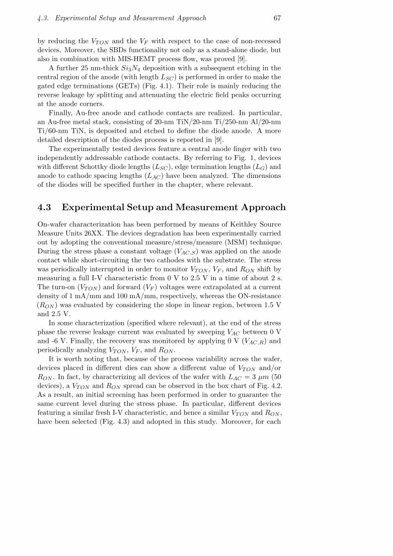
4.3. Experimental Setup and Measurement Approach 67
by reducing the VTON and the VF with respect to the case of non-recesseddevices. Moreover, the SBDs functionality not only as a stand-alone diode, butalso in combination with MIS-HEMT process flow, was proved [9].
A further 25 nm-thick Si3N4 deposition with a subsequent etching in thecentral region of the anode (with length LSC) is performed in order to make thegated edge terminations (GETs) (Fig. 4.1). Their role is mainly reducing thereverse leakage by splitting and attenuating the electric field peaks occurringat the anode corners.
Finally, Au-free anode and cathode contacts are realized. In particular,an Au-free metal stack, consisting of 20-nm TiN/20-nm Ti/250-nm Al/20-nmTi/60-nm TiN, is deposited and etched to define the diode anode. A moredetailed description of the diodes process is reported in [9].
The experimentally tested devices feature a central anode finger with twoindependently addressable cathode contacts. By referring to Fig. 1, deviceswith different Schottky diode lengths (LSC), edge termination lengths (LG) andanode to cathode spacing lengths (LAC) have been analyzed. The dimensionsof the diodes will be specified further in the chapter, where relevant.
4.3 Experimental Setup and Measurement Approach
On-wafer characterization has been performed by means of Keithley SourceMeasure Units 26XX. The devices degradation has been experimentally carriedout by adopting the conventional measure/stress/measure (MSM) technique.During the stress phase a constant voltage (VAC S) was applied on the anodecontact while short-circuiting the two cathodes with the substrate. The stresswas periodically interrupted in order to monitor VTON , VF , and RON shift bymeasuring a full I-V characteristic from 0 V to 2.5 V in a time of about 2 s.The turn-on (VTON ) and forward (VF ) voltages were extrapolated at a currentdensity of 1 mA/mm and 100 mA/mm, respectively, whereas the ON-resistance(RON ) was evaluated by considering the slope in linear region, between 1.5 Vand 2.5 V.
In some characterization (specified where relevant), at the end of the stressphase the reverse leakage current was evaluated by sweeping VAC between 0 Vand -6 V. Finally, the recovery was monitored by applying 0 V (VAC R) andperiodically analyzing VTON , VF , and RON .
It is worth noting that, because of the process variability across the wafer,devices placed in different dies can show a different value of VTON and/orRON . In fact, by characterizing all devices of the wafer with LAC = 3 µm (50devices), a VTON and RON spread can be observed in the box chart of Fig. 4.2.As a result, an initial screening has been performed in order to guarantee thesame current level during the stress phase. In particular, different devicesfeaturing a similar fresh I-V characteristic, and hence a similar VTON and RON ,have been selected (Fig. 4.3) and adopted in this study. Moreover, for each

68Chapter 4. Reliability of GaN-on-Si Schottky Barrier Diodes under ON-State
Stress
stress/recovery analysis different devices have been initially considered in orderto verify the statistical dispersion of the measurements.
0,45
0,50
0,55
0,60
0,65
0,70
0,75
0,80
V TO
N (V
)3,6
3,8
4,0
4,2
4,4
4,6
4,8
5,0
RON
RO
N (
mm
)
LSC = 6 mLAC = 3 mLG = 1.5 mT = 25 °C
VTON
Figure 4.2: Box chart for VTON and RON considering all device in the waferwith LSC = 6 µm, LG = 1.5 µm and LAC = 3 µm at T = 25 ◦C. Due toprocess variability across the wafer a VTON and RON spread is shown. VTONand RON were extrapolated at the current density of 1 mA/mm and at theanode cathode voltage of 2.5 V, respectively.
0 1 2 3 4 5 6 7 80,0
0,2
0,4
0,6
0,8
1,0
1,2
1,4
1,6
Discarder
DIE REF. DIE 3, 6, 28, 33, 44, 45, 49, etc. DIE 16, 24, 36, 50, etc.
AC(A
/mm
)
VAC (V)
T = 25 °C
SelectedVTON = 0.53 VVF = 1.25 VRON(2.5V) = 4.3 mm
Figure 4.3: Forward characteristics of the GET-SBDs. Due to the variabilityof the process along the wafer, a screening of devices featuring similar I-Vcharacteristics has been performed.

4.4. Simulation methodology 69
4.4 Simulation methodology
In order to evaluate the dependence of the ON-state degradation on diodegeometry and to understand the degradation mechanisms affecting the devicesparameters, experimental analyses combined with TCAD simulations, aimed atevaluating the electric fields distribution along the device, have been performed.
The simulated structure has been defined in Sentaurus TCAD simulator [40]considering the geometric characteristics and material properties of the devicesunder test (DUT). In particular, the Schottky barrier height, the ohmic contactresistance and the mobility degradation models have been properly set in orderto attain the same turn-on voltage (VTON ) and comparable forward currentlevels of the real devices. Moreover, the effect of the traps on the electric fielddistribution is accounted for in the simulation by considering donor-like trapsat the SiN/AlGaN interface (access and GET regions). As a result, a goodagreement between experimental and simulated I-V characteristics has beenobtained (Fig. 4.4).
0 2 4 610-11
10-9
10-7
10-5
10-3
10-1
101
(b)
Simulation Experimental
I AC (A
/mm
)
VAC (V)
LSC = 6 mLG = 1.5 mLAC = 10 mT = 25 °C
(a)0 2 4 6 8
0,0
0,1
0,2
0,3
0,4
0,5
0,6
I AC (A
/mm
)
VAC (V)
Figure 4.4: Comparison of the I-V characteristics in the case of simulated andexperimental device in logarithmic (a) and linear (b) scale. The simulatedstructure has been calibrated in order to get comparable current level of thereal device. As a result, an accurate electric field distribution can be evaluated.
4.5 Results and Discussion
4.5.1 Trapping/de-trapping mechanisms causing VTON degra-dation
AlGaN/GaN Schottky barrier diodes with LSC = 9 µm, LG = 1.5 µm, LAC =5 µm, and a finger width of 100 µm have been adopted for understanding the

70Chapter 4. Reliability of GaN-on-Si Schottky Barrier Diodes under ON-State
Stress
trapping/de-trapping mechanisms underneath the VTON degradation.
The turn-on voltage shift occurring during the ON-state stress and recoveryis shown in Fig. 4.5. Four devices, positioned in different dies and selectedas shown in Fig. 4.3, have been characterized under the same stress andrecovery conditions in order to prove a good reproducibility of the VTONdegradation induced by trapping/de-trapping mechanisms. During the stressphase, electrons are trapped in the region under the anode (Schottky junction)causing an increase of the Schottky barrier height, and hence of the VTON .Then, as the stress is removed (recovery phase) some defects are de-trappedand a partial VTON recovery occurs.
0 10 20 30 40 50 600
2
4
6
8
10
12
die_6 die_37 die_38 die_41
3.2 %
2nd cycle
V TON
(%)
Time (s) x103
VAC_S = 7 VVAC_R = 0 VTS = TR = 25 °C
1st cycle
4 %
Figure 4.5: Turn-on voltage shift during two cycles of ON-state stress andrecovery for four devices positioned in different dies. VTON was extracted atthe current density of 1 mA/mm and the following conditions were considered:VAC S = 7 V (during stress), VAC R = 0 V (during recovery), T = 25 ◦C (bothphases). The four samples show similar VTON degradation and recovery.
A second cycle of stress and recovery has been performed in order to un-derstand which kind of trapping/de-trapping mechanism occurs, by comparingthe two stress and recovery dynamics. It is worth noting that Fig. 4.6a and4.6b are representative of the average of four samples (reported in Fig. 4.5). Inorder to account for the statistics dispersion, the error bars were calculated as±3σ (standard deviation).
From the evolution of VTON reported in Fig. 4.6a, it is possible to distinguishtwo degradation phases characterized by different power slopes that may beassociated to two different trapping mechanisms. For stress time up to 20 s, thebuild-up of charge in pre-existing defects appears to be the dominant mechanismcausing the degradation, whereas afterwards, as discussed in subsection 4.5.3,the creation of new defects becomes the dominant one.

4.5. Results and Discussion 71
Based on Figs. 4.5, 4.6a, and 4.6b, it is possible to observe that: i) in bothdegradation cycles (Fig. 4.5) the relative degradation occurring during the first10 s of stress is comparable to the amount of the corresponding subsequentrecovery (≈ 4 % and ≈ 3.2 % for the first and second cycle, respectively);
100 101 102 103 104100
3x100
5x100
7x1009x100
1,1x101
n = 0.24
1st stress 2nd stress
V TON
(%)
Stress Time (s)
Stress conditions:VAC_S = 7 VT = 25 °C
n = 0.21
(a)
Error bar = ±
100 101 102 103 104100
3x100
5x100
7x1009x100
1,1x101
2nd recovery 1st recovery
V TON
(%)
Recovery Time (s)
Recovery conditions:VAC_R = 0 VT = 25 °C
Same defects are involved during the two recovery phases
(b)
Error bar = ±
Figure 4.6: Stress and recovery phase related to Fig. 4.5. The dual slope shownin the stress phase (a) is probably attributed to two different mechanisms,build-up of charges and new trap creation, precisely. ∆VTON degradationrelated to the second cycle is calculated with respect to the end of the firstrecovery phase. The two recovery phases show a similar dynamics (b), meaningthat same defects are involved in the de-trapping mechanism.
ii) for short stress times (≈ 10 s), the VTON degradation features the samedynamics (same slope) in both cycles (Fig. 4.6a); iii) the two recovery phasesexhibit the same trend (Fig. 4.6b). In conclusion, by considering together theseaspects, it is possible to conclude that the shift of the turn-on voltage in the

72Chapter 4. Reliability of GaN-on-Si Schottky Barrier Diodes under ON-State
Stress
first 10 s of stress and during the whole recovery phase, in both cycles, maybe mainly ascribed to the trapping and de-trapping of the same pre-existingdefects. In addition, these results suggest that pre-existing defects are thesource of the recoverable degradation component, whereas the new createddefects cause a quasi-permanent or slowly recoverable component.
Thanks to the adopted MSM technique the impact of degradation on reverseleakage during ON-state stress and recovery has been analyzed (Fig. 4.7). Aslight non-recoverable reduction of the reverse leakage after the ON-state stress,due to electrons trapping, is shown in Fig. 4.7. By trapping negative chargein the AlGaN barrier layer or at Si3N4/AlGaN interface, the 2DEG densityin the channel is reduced; therefore, as observed in [32], a reverse leakagereduction may occur.
0 -1 -2 -3 -4 -5 -610-11
10-10
10-9
10-8
10-7
10-6
10-5
Fresh Stressed Recovered
Rev
erse
Lea
kage
(A/m
m)
VAC (V)
Stress & Recovery conditions:VAC_S = 7 VVAC_R = 0 VTS = TR = 25 °C
Figure 4.7: Reverse leakage measured in fresh condition, after 104 s of stressand after 3 · 104 s of recovery. The electrons trapping during the ON-statestress lead to a slight reduction of the reverse leakage.
4.5.2 Voltage-dependence
It is worth noting that from here on, the reverse leakage measurement has notbeen performed in order to avoid a possible alteration of the defects state dueto negative voltage sweep. Moreover, given the limited statistical dispersionreported in Fig. 4.6, from here on (except where specified) a single device isused for each stress/recovery condition.
The VTON degradation for different stress voltages is reported in Fig. 4.8.As already discussed with reference to Fig. 4.6a, two degradation phases areevident, and the first one may be attributed to pre-existing traps filling. Indeed,by increasing the stress voltage, the end of the first degradation phase (i.e. thechange of the power slope) occurs for shorter stress time. This is expectedwhen a fixed number of traps, with a fixed energy level, are present in the

4.5. Results and Discussion 73
fresh device. By applying a higher stress bias a faster charge trapping occurs,leading to a larger degradation and to a faster filling of the available traps.
Finally, as it is possible to observe in Fig. 4.9, the voltage-dependence ofboth turn-on and forward voltage degradations can be modeled by a powerlaw.
100 101 102 103 104100
101
102
n = 0.07
VAC_S = 8 V VAC_S = 7 V VAC_S = 6 V VAC_S = 5 V VAC_S = 4 V
V TO
N (%
)
Stress Time (s)
n = 0.19 - 0.30
T = 25 °C
Figure 4.8: VTON shift for different ON-state stress conditions. By stressing athigher voltage, the pre-existing traps filling is faster. As a result, the changeof the logarithmic slope occurs for shorter stress time.
3 4 5 6 7 8 9100
101
102
n = 0.98
V TON (%
)
Stress Voltage (V)
Power dependence
The degradation is extracted after 104 s of DC stressat T = 25 °C
n = 0.91
100
101
102
V F (%
)
Figure 4.9: Turn-on and forward voltage degradation versus stress voltage. Apower dependence is observed for both parameters.
On the other hand, the evolution of ∆RON and its dependence on stressbias are much more complex, and chaotic, compared to the case of turn-onvoltage. Causes and reasons will be more deeply explored in subsection 4.5.4.

74Chapter 4. Reliability of GaN-on-Si Schottky Barrier Diodes under ON-State
Stress
4.5.3 Temperature-dependence
100 101 102 103 104100
101
102
T = 50 °C T = 75 °C T = 100 °C T = 125 °C
V TON(%
)Stress Time (s)
VAC_S = 5 V
power law
Figure 4.10: Turn-on voltage shift for different temperatures stress.
28 30 32 34 36 38100
101
102
without recesswith recess
Ea = 0.098 eV
V TON (%
)
1/kT (eV-1)
Fitting : VTON = A * exp (-Ea/kT)
After 104 s of stress at V AC_S = 5 V
Ea = 0.093 eV
(b)
Figure 4.11: Arrhenius plot. The VTON shift has been extracted at the end ofthe stress (104 s) in devices with (circle) and without (square) anode recess. Byconsidering the database of the deep levels in GaN- and AlGaN-based devices[41], the activation energy of ≈ 0.09 eV is linked to the nitrogen vacancies.
The role of the temperature on the ON-state degradation has been investigatedon the same devices analyzed in the two previous sections. Fig. 4.10 showsthe shift of the turn-on voltage as a function of the temperature. It can benoticed that, by stressing at temperatures higher than 25 ◦C, the dual slopeof the VTON degradation is not clearly observed (Fig. 4.10), contrary to thecase of room temperature (Fig. 4.8). As a matter of fact, by increasing the

4.5. Results and Discussion 75
temperature the process of filling of pre-existing traps, according to results,may be shorter than 1 s suggesting the presence of very shallow pre-existingtraps. Moreover, curves at different temperatures feature a similar slope (0.08)that is similar to the second degradation phase of the room temperature casereported in Fig. 4.8.
By considering the Arrhenius plot of Fig. 4.11, an effective activation energyof 0.093 eV has been extracted from VTON degradation. The database of thedeep levels in GaN- and AlGaN-based devices (see [41]) suggests that trapshaving an activation energy of 0.09 eV can be ascribed to the nitrogen vacancies.A similar value has been found by Bisi et al. in AlGaN/GaN HEMT [41],by means of the current transient investigation at several temperature levels,linking these traps to the AlGaN barrier in the region under the gate.
In the case of diodes, the VTON shift under forward stress is ascribedto an increase of Schottky barrier height and features a similar activationenergy (0.093 eV). Hence, it can be assumed that traps, responsible for VTONdegradation, are located in the AlGaN barrier layer under the anode metal.An activation energy of 0.093 eV suggests that the traps are fairly shallow, andhence they should feature a short trapping/de-trapping time constant. On thecontrary, in this case the activation energy is extracted after 104 s of stress.This observation confirms that the creation of new defects is the responsiblemechanism causing the degradation.
In order to understand which is the cause of the nitrogen vacancies, a studyof the temperature dependence of VTON degradation has been performed alsoon devices without anode recess (Fig. 4.11). By considering the Arrhenius plotof Fig. 4.11, we can observe that: i) devices without recess show a comparable(or slightly higher) VTON degradation; ii) the VTON shift in both typologies ofdevice is induced by the same kind of traps because of the similar activationenergies. As a result, nitrogen vacancies are not caused by the recess processbut probably are linked to crystal quality of the AlGaN barrier layer. Byavoiding the anode recess, the AlGaN barrier under the anode metal is thicker;as a consequence, a larger number of bulk defects are present, leading to aslightly higher VTON degradation.
Finally, the study of the RON degradation for different temperatures isshown in Fig. 4.12a. It seems from this figure that no RON degradation increaseis observed for higher temperatures. On the other hand, from Fig. 4.12b, itis possible to observe a decrease of the ON-current during the stress and ahuge recovery happening during each measurement phase. It is well knownthat by increasing the temperature, the de-trapping mechanism becomes faster,and hence the de-trapping time constant could be lower than the delay timeintroduced by measurement setup. As a result, the ON-resistance degradesduring the stress but it is not possible to catch the real degradation with thistechnique. This suggests that RON and VTON degradations are due to differentdefects, however, as previously anticipated, an in-depth investigation of RON

76Chapter 4. Reliability of GaN-on-Si Schottky Barrier Diodes under ON-State
Stress
degradation will be shown in subsection 4.5.4.It is worth noting that SBDs in actual application are forced to work with
fixed ON-current, rather than with fixed VAC . However, the change of theON-current, during the stress (see Fig. 4.12b) at fixed voltage, is relatively low.
100 101 102 103 104-2
-1
0
1
2
3 T = 50 °C T = 75 °C T = 100 °C T = 125 °C
RO
N(%
)
Stress Time (s)
VAC_S = 5 V
(a)
10-1 100 101 102 103 1040,95
0,96
0,97
0,98
0,99
1,00
Nor
mal
ized
I AC (a
.u.)
Stress Time (s)
VAC_S = 5 VT = 125 °C
Current during the stress
Fast recovery
(b)
Figure 4.12: RON degradation at different temperatures (a). By increasingthe temperature, as the stress voltage is removed in order to perform an IVcharacteristics, a fast recovery of the ON-current is observable (b). As a result,no RON degradation is shown (a).
4.5.4 Anode to cathode spacing length (LAC) dependence
AlGaN/GaN Schottky barrier diodes with LSC = 6 µm, LG = 1.5 µm, differentLAC (3, 10 and 20 µm), and a finger width of 100 µm have been adoptedfor understanding the LAC dependence on the ON-state degradation. Byreducing LAC , the devices show an improved ON-characteristic due to lower

4.5. Results and Discussion 77
ON-resistance (Fig. 4.13). On the other hand, for high stress voltages, thehigher electric fields between anode and cathode accelerate the degradationmechanisms allowing to understand the causes underneath the device degrada-tion.
0,0 0,5 1,0 1,5 2,0 2,50,0
0,1
0,2
0,3
0,4
0,5LSC = 6 mLG = 1,5 m
Fresh conditionT = 150 °C
I AC (A
/mm
)
VAC (V)
LAC = 3 m LAC = 10 m LAC = 20 m
Figure 4.13: I-V characteristics of devices featuring different anode to cath-ode spacing lengths. By reducing LAC , the devices show an improved ON-characteristic due to lower ON-resistance.
1 2 3 4 5 6 7100
101
102
103
104
105
106
107
108
109
10 years
LAC = 20 m LAC = 10 m LAC = 3 m
Life
time (s
)
VAC (V)
Failure cond:VF = 5 %
T = 150 °C
VF = VTON+ RON* IAC
Figure 4.14: Lifetime estimation as function of anode-cathode spacing lengths(LAC). The failure criterion is considered as 5 % shift of the forward voltage(∆VF ) at the temperature of 150 ◦C. By increasing the anode to cathode stressvoltage (VAC), shorter devices show a higher VF degradation.
The analysis of the ON-state degradation at different stress biases, by

78Chapter 4. Reliability of GaN-on-Si Schottky Barrier Diodes under ON-State
Stress
means of constant voltage-stress method, allowed to estimate the lifetime of theAlGaN/GaN-on-Si GET-SBDs at the temperatures of 150 ◦C, as reported inFig. 4.14. The lifetime has been extrapolated by considering the forward voltagedegradation since it takes into account both VTON and RON degradations bythe following relationship:
∆VF = ∆VTON + ∆RON · IAC (4.1)
In particular, a threshold ∆VF value of the 5 % in 10 years has been selected.Four devices with a similar fresh I-V characteristic have been stressed for eachLAC . However, the reproducibility of the device degradation, due to ON-statestress, has been proven in section 4.5.1 by stressing different selected deviceswith the same stress conditions. By analyzing Fig. 4.14, for high stress voltages,short anode-cathode devices exhibit a significant larger degradation in theforward voltage (VF ), i.e. lower lifetime, with respect to wide anode-cathodedevices. Intuitively, this can be ascribed to higher electric fields under theSchottky contact and/or in the anode to cathode access region. Interestingly,such a difference is not observed for low stress voltage and a crossing point isobserved around VAC = 1.2 V. Hence, the three analyzed LAC lengths giverise to different power law fittings.
Since the ∆VF is due to the combined effect of the turn-on voltage (VTON )and on-resistance (RON ) degradation by the relationship shown in Eq. 4.1,their contributions are separately evaluated in Fig. 4.15 and 4.16, respectively.
100 101 102 103 104100
101
102
VAC = 2.5 V
VAC = 6.5 V
V TON (%
)
Stress Time (s)
LAC = 3 m LAC = 10 m LAC = 20 m
T = 150 °C
Figure 4.15: Turn-on voltage degradation, due to ON-state stress, evaluatedfor different LAC at VAC = 6.5 V (filled markers) and VAC = 2.5 V (emptymarkers). VTON was extrapolated at the current density of 1 mA/mm. Asthe stress voltage increases, a higher difference in VTON degradation, betweenshort and long device, is shown.

4.5. Results and Discussion 79
Although a significant VTON degradation is observed with stress voltage-and LAC-dependence (Fig. 4.15), in the case of the RON (Fig. 4.16), a sizabledegradation is only observable for VAC = 6.5 V and LAC = 3 µm. This suggeststhat different sources of degradation affect VTON and RON .
100 101 102 103 104-5
0
5
10
15
20
25
30
35
VAC = 6.5 VT = 150 °C
RO
N (%
)
Stress Time (s)
LAC = 3 m LAC = 10 m LAC = 20 m
Figure 4.16: ON-resistance degradation evaluated for VAC = 6.5 V and differentLAC , by considering the slope in linear region, between 1.5 V and 2.5 V. Inspite of VTON degradation (see Fig. 4.15), devices equal to or longer than 10µm do not show RON shift. As a result, different mechanisms of degradationaffect RON and VTON .
100 101 102 103 104-10
-5
0
5
10
15
20
25
30
RO
N (%
)
Stress Time (s)
T = 25 °C T = 130 °C T = 90 °C T = 140 °C T = 110 °C T = 150 °C T = 120 °C
VAC = 6.5 VLAC = 3 m
Figure 4.17: RON degradation evaluated at different temperatures. A significanttemperature dependence is observed. Considerable RON degradation starts tooccur only for T > 110 ◦C.
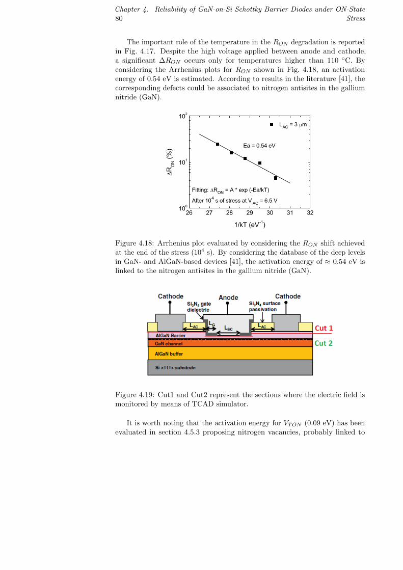
80Chapter 4. Reliability of GaN-on-Si Schottky Barrier Diodes under ON-State
Stress
The important role of the temperature in the RON degradation is reportedin Fig. 4.17. Despite the high voltage applied between anode and cathode,a significant ∆RON occurs only for temperatures higher than 110 ◦C. Byconsidering the Arrhenius plots for RON shown in Fig. 4.18, an activationenergy of 0.54 eV is estimated. According to results in the literature [41], thecorresponding defects could be associated to nitrogen antisites in the galliumnitride (GaN).
26 27 28 29 30 31 32100
101
102
LAC = 3 m
Ea = 0.54 eV
Fitting: RON = A * exp (-Ea/kT)
After 104 s of stress at V AC = 6.5 V
RO
N (%
)
1/kT (eV-1)
Figure 4.18: Arrhenius plot evaluated by considering the RON shift achievedat the end of the stress (104 s). By considering the database of the deep levelsin GaN- and AlGaN-based devices [41], the activation energy of ≈ 0.54 eV islinked to the nitrogen antisites in the gallium nitride (GaN).
Figure 4.19: Cut1 and Cut2 represent the sections where the electric field ismonitored by means of TCAD simulator.
It is worth noting that the activation energy for VTON (0.09 eV) has beenevaluated in section 4.5.3 proposing nitrogen vacancies, probably linked to

4.5. Results and Discussion 81
crystal quality of the AlGaN barrier, as defects responsible for the degradationof VTON . However, it is again proved that RON and VTON degradations aredue to different kind of defects.
-4 -3 -2 -1 0 1 2 3 4
-0,8
-0,4
0,0
0,4
0,8
1,2LSC LG
GET
LAC = 3 m LAC = 10 m LAC = 20 m
Verti
cal E
_Fie
ld (M
V/cm
)
Position along SiN-Metal/AlGaN interface ( m)
LAC
VAC = 6.5 VT = 150 °CCut 1
Figure 4.20: Vertical electric field profile in the AlGaN barrier close to interfacewith SiN and metal (cut 1 in Fig. 4.19) for high stress voltage. For high VACshorter devices show a larger electric field only in the region under the anode(Schottky) contact (LSC) leading to a higher VTON degradation (Fig. 4.15).
1,5 2,0 2,5 3,0 3,5 4,00,0
-0,1
-0,2
LSC = Schottky contact
LAC = 3 m LAC = 10 m LAC = 20 m
Long
itudi
nal E
_Fie
ld (k
V/cm
)
Position along Metal/AlGaN interface ( m)
VAC = 6.5 VT = 150 °CCut 1
Figure 4.21: Longitudinal electric field profile in the AlGaN barrier close tointerface with metal (cut 1 in Fig. 4.19). Despite the high anode voltage,low values of the longitudinal component of the electric field is noticeable,suggesting that it is irrelevant for the VTON degradation.
In order to understand the sources triggering VTON and RON degradation,TCAD simulations [40], aimed at evaluating the electric fields distributions

82Chapter 4. Reliability of GaN-on-Si Schottky Barrier Diodes under ON-State
Stress
in the structure, have been performed. By considering the cut 1 of Fig. 4.19,the vertical component of the electric field at the SiN/AlGaN and at themetal/AlGaN (Schottky contact) interface, in the case of VAC = 6.5 V fordifferent LAC , is shown in Fig. 4.20. By changing LAC , the only difference isobserved under the Schottky contact region near the edge termination (GET),where shorter devices exhibit a higher electric field and hence a higher VTONdegradation with respect to longer devices (Fig. 4.15). By observing Fig. 4.21,it is worth noting that in this region, the longitudinal component of the electricfield is negligible, hence it is not able to contribute to the VTON degradation.
The LAC dependence of the RON degradation cannot be explained by thevertical component of the electric field since it is unchanged in the GET andanode-cathode spacing regions (Fig. 4.20) where the contribution to the overallon-resistance is dominant. Instead, by observing Fig. 4.22 it is possible tonote a significant difference, between short and long device, for the electricfield component longitudinal to current flow (cut 2 of Fig. 4.19). The linkbetween longitudinal electric field and RON degradation is demonstrated inFig. 4.23 and 4.24 by applying different stress voltages on devices with LAC =5 µm. For electric fields higher than ≈ 6 kV/cm the RON starts to degrade.This dependence on the longitudinal electric field automatically implies adependence on the current value because of their correlation. In particular, foran electric field of ≈ 6 kV/cm at T = 150 ◦C these devices feature an ON-statecurrent density of ≈ 0.45 A/mm.
-4 -3 -2 -1 0 1 2 3 40
-3
-6
-9
-12
-15
-18LSC LG
GETLAC = 3 mLAC = 10 mLAC = 20 m
Long
itudi
nal E
_Fie
ld (k
V/cm
)
Position along the channel ( m)
LAC
VAC = 6.5 VT = 150 °CCut 2
Figure 4.22: Longitudinal electric field profile in the GaN channel close tointerface with AlGaN barrier (cut 2), for high stress voltage. By reducing LACa larger electric field difference, between short and long devices, is only shownin the LG and LAC regions. As a result, for high VAC , larger ∆RON is shownfor shorter devices.

4.5. Results and Discussion 83
100 101 102 103 104-5
0
5
10
15
20
25
30
35
T = 150 °CLAC = 5 m
RO
N (%
)
Stress Time (s)
VAC = 8 V VAC = 7 V VAC = 4 V
Figure 4.23: ∆RON evaluated with different anode bias stress on devices withLAC = 5 µm. The RON degradation is due to combined effect of temperatureand longitudinal electric field (mainly under the LG region).
-5 -4 -3 -2 -1 0 1 2 3 40
-2-4-6-8
-10-12-14-16-18
LSCLG
VAC = 8 V VAC = 7 V VAC = 4 V
Long
itudi
nal E
_Fie
ld (k
V/cm
)
Position along the channel ( m)
LAC = 5 m
T = 150 °CCut 2
Figure 4.24: Longitudinal electric field profile (cut 2) related to the stressconditions of Fig. 4.23. A correlation between electric field and ∆RON is shown.Moreover, by comparing Fig. 4.23 and 4.16, despite the different LAC and VAC ,a similar ∆RON (≈ 30 %) is obtained under a similar electric field (Fig. 4.24and 4.24, respectively).
The existence of a critical longitudinal electric field is in agreement withFig. 4.22 and 4.16, where no degradation is observed for an electric field lowerthan ≈ 6 kV/cm. Moreover, devices with different LAC (3 µm or 5 µm)featuring the same longitudinal electric field (11 kV/cm in Fig. 4.22 and 4.24),show a similar RON degradation (≈ 30 %), as reported in Fig. 4.15 and 4.23.This confirms that the cause of the RON shift is due to combined effect of
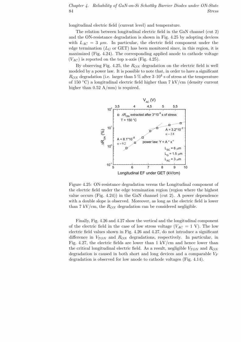
84Chapter 4. Reliability of GaN-on-Si Schottky Barrier Diodes under ON-State
Stress
longitudinal electric field (current level) and temperature.
The relation between longitudinal electric field in the GaN channel (cut 2)and the ON-resistance degradation is shown in Fig. 4.25 by adopting deviceswith LAC = 3 µm. In particular, the electric field component under theedge termination (LG or GET) has been monitored since, in this region, it ismaximized (Fig. 4.24). The corresponding applied anode to cathode voltage(VAC) is reported on the top x-axis (Fig. 4.25).
By observing Fig. 4.25, the RON degradation on the electric field is wellmodeled by a power law. It is possible to note that, in order to have a significantRON degradation (i.e. larger than 5 % after 3 ·104 s of stress at the temperatureof 150 ◦C) a longitudinal electric field higher than 7 kV/cm (density currenthigher than 0.52 A/mm) is required.
5 6 7 8 9 1010-1
100
101
102
A = 8.1*10 -8
A = 3.2*10 -2
RON extracted after 3*10 4 s of stress T = 150 °C
RO
N (%
)
Longitudinal EF under GET (kV/cm)
LSC = 6 mLG = 1.5 mLAC = 3 m
power law: Y = A * x
3,5 4 4,5 5 5,5
VAC (V)
Figure 4.25: ON-resistance degradation versus the Longitudinal component ofthe electric field under the edge termination region (region where the highestvalue occurs (Fig. 4.24)) in the GaN channel (cut 2). A power dependencewith a double slope is observed. Moreover, as long as the electric field is lowerthan 7 kV/cm, the RON degradation can be considered negligible.
Finally, Fig. 4.26 and 4.27 show the vertical and the longitudinal componentof the electric field in the case of low stress voltage (VAC = 1 V). The lowelectric field values shown in Fig. 4.26 and 4.27, do not introduce a significantdifference in VTON and RON degradations, respectively. In particular, inFig. 4.27, the electric fields are lower than 1 kV/cm and hence lower thanthe critical longitudinal electric field. As a result, negligible VTON and RONdegradation is caused in both short and long devices and a comparable VFdegradation is observed for low anode to cathode voltages (Fig. 4.14).
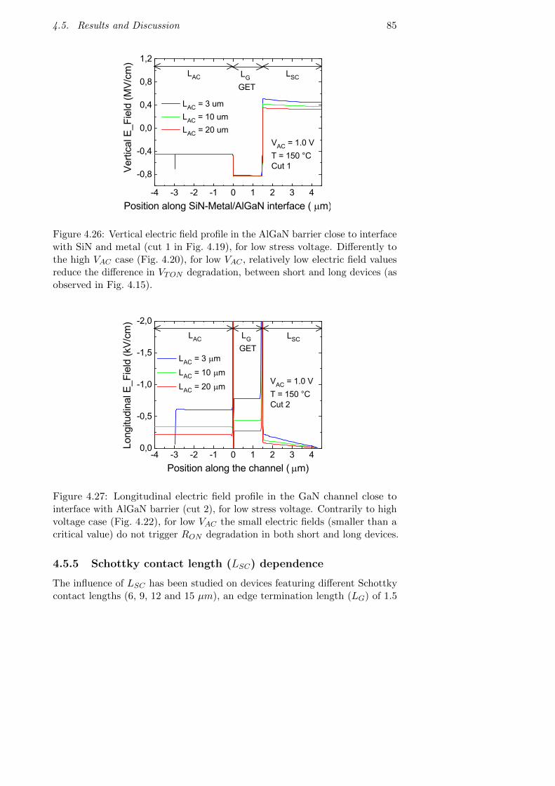
4.5. Results and Discussion 85
-4 -3 -2 -1 0 1 2 3 4
-0,8
-0,4
0,0
0,4
0,8
1,2LSC LG
GET
LAC = 3 um LAC = 10 um LAC = 20 um
Verti
cal E
_Fie
ld (M
V/cm
)
Position along SiN-Metal/AlGaN interface ( m)
LAC
VAC = 1.0 VT = 150 °CCut 1
Figure 4.26: Vertical electric field profile in the AlGaN barrier close to interfacewith SiN and metal (cut 1 in Fig. 4.19), for low stress voltage. Differently tothe high VAC case (Fig. 4.20), for low VAC , relatively low electric field valuesreduce the difference in VTON degradation, between short and long devices (asobserved in Fig. 4.15).
-4 -3 -2 -1 0 1 2 3 40,0
-0,5
-1,0
-1,5
-2,0LSC LG
GET LAC = 3 m LAC = 10 m LAC = 20 m
Long
itudi
nal E
_Fie
ld (k
V/cm
)
Position along the channel ( m)
LAC
VAC = 1.0 VT = 150 °CCut 2
Figure 4.27: Longitudinal electric field profile in the GaN channel close tointerface with AlGaN barrier (cut 2), for low stress voltage. Contrarily to highvoltage case (Fig. 4.22), for low VAC the small electric fields (smaller than acritical value) do not trigger RON degradation in both short and long devices.
4.5.5 Schottky contact length (LSC) dependence
The influence of LSC has been studied on devices featuring different Schottkycontact lengths (6, 9, 12 and 15 µm), an edge termination length (LG) of 1.5

86Chapter 4. Reliability of GaN-on-Si Schottky Barrier Diodes under ON-State
Stress
µm, an anode to cathode spacing (LAC) of 10 µm, and a finger width of 100µm.
0 1 2 3 4 5 6 7 80,0
0,2
0,4
0,6
0,8
1,0
1,2
IAC
(A/m
m)
LAC = 10 mLG = 1.5 mT = 25 °C
LSC = 6 m 9 m 12 m 15 m
VAC (V)
Figure 4.28: I-V characteristics of devices featuring different Schottky contactlengths. Due to the current crowding phenomenon occurring at the anodecontact, the I-V curves are similar for different LSC .
0,7
0,8
0,9
1,0
1,1
(b)
LSC = 6 m ; LAC = 5 mLG = 1.5 m ; T = 150 °C
VAC = 6.5 V VAC = 4.5 V VAC = 2.5 V VAC = 1.0 V
Verti
cal E
_Fie
ld (M
V/cm
)
(a)
0,0 0,5 1,0 1,5 2,0 2,5 3,00,0
0,5
1,0
1,5
2,0
2,5
LSC center
X along the Schottky junction ( m)
Verti
cal e
Cur
rent
den
sity
(A
/cm
2 ) x 1
04
LSC edge
Cut 1
Figure 4.29: Simulated vertical electric field (a) and electron current density(b) under the Schottky contact close to the metal/AlGaN interface (cut 1 ofFig. 4.19). By increasing the anode to cathode bias (VAC) a vertical currentflow confinement is shown (b).

4.5. Results and Discussion 87
By observing Fig. 4.28, it is possible to note that same I-V characteristicsare found for devices with different LSC . This behavior is related to the electricfield distribution, and hence to the current density distribution (Fig. 4.29b),under the anode contact.
In forward operation mode, by increasing the anode to cathode bias (VAC),the electric field tends to be higher at the edge of Schottky contact, causinga current crowding at the contact edge (current transfer length) [42]. As amatter of fact, for VAC higher than 2.5 V the anode current is limited by thecontact resistance. Hence, the increase of LSC does not lead to significantcurrent improvement.
It is worth noting that, only half structure (hence half LSC) has beenconsidered in the simulations because of the device symmetry.
In order to understand how the Schottky contact length affects the diodereliability, a study of the degradation mechanisms has been performed fordevices with different LSC . The analysis of the ON-state degradation atdifferent stress biases, by means of constant voltage-stress method, allows toestimate the lifetime of the AlGaN/GaN-on-Si GET-SBDs at the temperaturesof 150 ◦C, as reported in Fig. 4.30. As in the previous section, the lifetime hasbeen extrapolated by considering the 5 % of ∆VF in 10 years, since it takesinto account both VTON and RON degradations.
1 2 3 4 5 6 7103
104
105
106
107
108
109
LAC = 10 mLG = 1.5 mT = 150 °C
10 years LSC = 6 m LSC = 9 m LSC = 12 m LSC = 15 m
Life
time (s
)
VAC_S (V)
Fail. cond.:VF = 5 %
Y = A * x-
Figure 4.30: Lifetime estimation as a function of the Schottky contact lengths(LSC). The failure criterion is considered as 5 % shift of the forward voltage(∆VF ) at the temperature of 150 ◦C. By reducing the anode to cathode stressvoltage (VAC S), shorter devices show a lower VF degradation leading to alonger lifetime.
The typical operating bias for the devices under test corresponds to SBDforward voltage (VF ), i.e. around 1.2 V. However, in order to perform a study
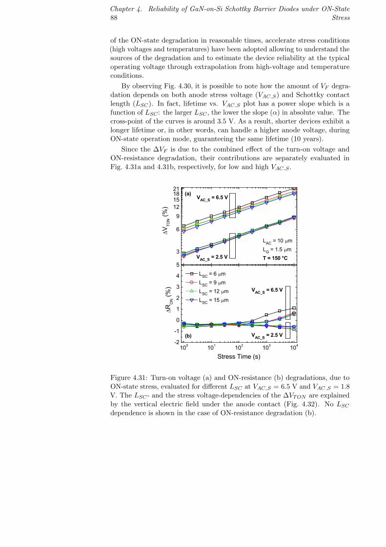
88Chapter 4. Reliability of GaN-on-Si Schottky Barrier Diodes under ON-State
Stress
of the ON-state degradation in reasonable times, accelerate stress conditions(high voltages and temperatures) have been adopted allowing to understand thesources of the degradation and to estimate the device reliability at the typicaloperating voltage through extrapolation from high-voltage and temperatureconditions.
By observing Fig. 4.30, it is possible to note how the amount of VF degra-dation depends on both anode stress voltage (VAC S) and Schottky contactlength (LSC). In fact, lifetime vs. VAC S plot has a power slope which is afunction of LSC : the larger LSC , the lower the slope (α) in absolute value. Thecross-point of the curves is around 3.5 V. As a result, shorter devices exhibit alonger lifetime or, in other words, can handle a higher anode voltage, duringON-state operation mode, guaranteeing the same lifetime (10 years).
Since the ∆VF is due to the combined effect of the turn-on voltage andON-resistance degradation, their contributions are separately evaluated inFig. 4.31a and 4.31b, respectively, for low and high VAC S .
3
6
912151821
VAC_S = 2.5 V
LAC = 10 mLG = 1.5 mT = 150 °C
LSC = 6 m LSC = 9 m LSC = 12 m LSC = 15 m
V TON (%
)
VAC_S = 6.5 V(a)
100 101 102 103 104-2
-1
0
1
2
3
4
5
(b)
VAC_S = 6.5 V
VAC_S = 2.5 V
RO
N (%
)
Stress Time (s)
Figure 4.31: Turn-on voltage (a) and ON-resistance (b) degradations, due toON-state stress, evaluated for different LSC at VAC S = 6.5 V and VAC S = 1.8V. The LSC- and the stress voltage-dependencies of the ∆VTON are explainedby the vertical electric field under the anode contact (Fig. 4.32). No LSCdependence is shown in the case of ON-resistance degradation (b).

4.5. Results and Discussion 89
By focusing on the ∆VTON (Fig. 4.31a), a stress voltage- and a LSC-dependence is shown. In particular, for VAC S = 6.5 V shorter devices showa larger VTON degradation, whereas for VAC S = 1..8 V the LSC-dependenceof ∆VTON is negligible and seems to reverse for lower stress voltages. Thisbehavior is explained by the vertical component of the electric field in theregion under the Schottky contact (Fig. 4.32). By applying 6.5 V on the anodecontact, a high electric field peak occurs at the corner between edge terminationand Schottky contact (origin in Fig. 4.32). Moreover, the peak is higher forshorter LSC , leading to a larger VTON degradation.
0 1 2 3 4 5 6 7 80,5
0,6
0,7
0,8
0,9
1,0
1,1
Cut 1
LAC = 10 mLG = 1.5 mT = 150 °C
LSC = 6 m LSC = 15 m
VAC = 1.0 V
Verti
cal E
lect
ric F
ield
(MV/
cm)
X along the Schottky junction ( m)
VAC = 6.5 V
LSC edge
Figure 4.32: Vertical electric field profile in the AlGaN barrier close to interfacewith metal (cut 1 in Fig. 4.19), for high and low anode voltages. For highVAC a higher electric field peak occurs in shorter devices leading to a largerVTON degradation (Fig. 4.31a). On the other hand, for low VAC , relatively lowelectric field values do not introduce a difference in VTON degradation. Onthe contrary, due to uniform electric field distribution, longer devices may beaffected by a larger ∆VTON .
In the case of low anode bias, it is thought that the lower electric fieldvalues, found for both LSC lengths, have a small impact on VTON degradation.On the contrary, since the electric field distribution and the electron currentdensity are approximately uniform along the Schottky junction (Fig. 4.32 VAC= 1 V or Fig. 4.29 VAC = 2.5 V and lower), a longer anode contact may leadto a larger VTON degradation.
By focusing on the ON-resistance degradation (Fig. 4.31b), it is possible tonote that, for both high (6.5 V) and low (1.8 V) stress voltages, the ∆RONis negligible (around ± 1 %) and no appreciable LSC dependence is observed.This is in agreement with the results discussed in the previous section, where ithas been shown that the source triggering RON degradation is the longitudinal

90Chapter 4. Reliability of GaN-on-Si Schottky Barrier Diodes under ON-State
Stress
component of the electric field in the regions where the contribution to theoverall ON-resistance is dominant, such as edge termination (GET) and anodeto cathode access (LAC) regions. Moreover, it has been shown that with atemperature operation of 150 ◦C, an electric field higher than ≈ 7 kV/cm isneeded in order to achieve a significant RON degradation. Fig. 4.33 shows thelongitudinal component of the electric fields related to the stress conditionsof Fig. 4.31b. By applying a high stress voltage (6.5 V), the electric field,in particular under the GET region, is lower than 7 kV/cm and no LSCdependence is shown.
-10 -8 -6 -4 -2 0 2 4 60
-1
-2
-3
-4
-5
-6
-7
-8
LSCLG = 1.5 m
LSC = 6 m LSC = 15 m
Long
itudi
nal E
_Fie
ld (k
V/cm
)
Position along the channel ( m)
LAC = 10 m
VAC = 6.5 VT = 150 °CCut 2
Figure 4.33: Longitudinal electric field profile (cut 2 in Fig. 4.19) with ananode bias of 6.5 V in the case of the shortest and longest device. By applyinga high anode bias (6.5 V), the longitudinal electric field is lower than 7 kV/cm,hence negligible degradation is shown.
Overall, by changing the Schottky contact length only the turn-on voltagedegradation is affected. In particular, by analyzing Fig. 4.29, 4.30 and 4.32,for VAC > 4 V the vertical electric field is confined to the anode corner anda higher peak occurs in shorter devices, leading to a larger ∆VTON . On theother hand, for VAC < 3 V, the electric field and the current density (Fig. 4.29)tend to be uniform in the overall Schottky junction. As a result, longer diodes,featuring a larger Schottky contact area, may be subject to a larger VTONdegradation.
4.5.6 Edge termination length (LG) dependence
AlGaN/GaN Schottky barrier diodes with LSC = 6 µm, different LG (1, 1.5,and 2 µm), LAC = 5 µm, and a finger width of 100 µm have been adopted forunderstanding the LG dependence on the ON-state degradation. The limiteddevices availability has dictated the choice to use diodes featuring a different

4.5. Results and Discussion 91
LAC with respect to those investigated in section 4.5.5. However, in the caseof LG = 1 µm and LG = 2 µm, more devices (7 for each LG), positionedin different dies but featuring a similar I-V characteristic in fresh condition,have been characterized under the same stress condition in order to verify thestatistical dispersion of the measurements, and to prove a good reproducibilityof the device degradation induced by trapping/de-trapping mechanisms.
In AlGaN/GaN-based devices, the main contribution to the overall ON-resistance comes from the two-dimensional electron gas (2DEG) in the accessregion. In the case of GET-SBDs, the RON is mainly attributable to theregion between the anode and cathode contacts. Therefore, by reducing LG,an improved forward characteristics, due to lower RON , is attained (Fig. 4.34).
0,0 0,5 1,0 1,5 2,0 2,50,0
0,1
0,2
0,3
0,4
0,5
0,6
I AC (A
/mm
)
RON @ 2.5 V4.8 mm5.3 mm5.8 mm
(b)
VAC (V)
LG = 1.0 m LG = 1.5 m LG = 2.0 m
T = 100 °CLSC = 6 mLAC = 5 m
Figure 4.34: I-V characteristics of devices featuring different edge terminationlengths. By reducing LG, the devices show an improved ON-characteristic dueto lower ON-resistance.
The turn-on voltage and the ON-resistance degradations, in the case ofVAC S = 2.5 V at T = 100 ◦C, are shown in Fig. 4.35a and Fig. 4.35b,respectively. It is worth noting that Fig. 4.35a and Fig. 4.35b are representativeof the average of seven samples (except for the case LG = 1.5 µm). In orderto account for the statistics dispersion, the error bars were calculated as ± 3σ(standard deviation).
A LG dependence is only shown in the case of ∆VTON (Fig. 4.35a) becauseof the increasing electric field in the region under the anode contact when LGis reduced (Fig. 4.36a). Moreover, due to lower RON , devices with shorter LGfeature a higher current density (Fig. 4.36b). As a result, the combined effectof large field and current density may cause a larger VTON degradation.
From the evolution of VTON reported in Fig. 4.35a, it is possible to dis-tinguish two degradation phases characterized by different power slopes. The

92Chapter 4. Reliability of GaN-on-Si Schottky Barrier Diodes under ON-State
Stress
reasons for this phenomenon have been discussed in section 4.5.2. In particu-lar, the first degradation phase has been linked to the build-up of charge inpre-existing defects, whereas new defects are created during the second one.Moreover, it has been shown that, the change of the power slope is stressvoltage-dependent.
3
6
9121518
(b)
LSC = 6 mLAC = 5 mT = 100 °CVAC_S = 2.5 V
LG = 1.0 m LG = 1.5 m LG = 2.0 m
V TON (%
)
(a)
Error bar = ±
100 101 102 103 104-0,8
-0,4
0,0
0,4
0,8
1,2
1,6
2,0
R
ON (%
)
Stress Time (s)
Figure 4.35: Turn-on voltage (a) and ON-resistance (b) degradations, due toON-state stress, evaluated for different LG at VAC S = 2.5 V and T = 100 ◦C.A LG dependence is only shown in the case of ∆VTON . In order to verify thestatistical dispersion of the measurements, and to prove a good degradationreproducibility, seven devices for each LG (except LG = 1.5 µm), have beencharacterized. The error bars represent the standard deviation (± 3σ).
By referring to Fig. 4.35b the RON degradation is limited (< 0.8 %) because,as in the case of LSC dependence, the longitudinal component of the electricfield (cut 2 in Fig. 4.19) is lower than 7 kV/cm since a low voltage is applied onthe anode (VAC S = 2.5 V). Consequently, due to small RON shift, the amountof degradation can be affected by different sources of error possibly induced byexperimental set-up, measurement technique, device variability, etc. In fact,by observing Fig. 4.35b, large error bars are shown compared to the measuredexpected value.
As a result, for the adopted stress conditions, the RON degradation is

4.5. Results and Discussion 93
not well reproducible and it is therefore impossible to identify the underlyingphysical mechanism. However, by deeply investigate the RON degradation,it has been shown in section 4.5.4 that: i) the ON-resistance degradation islinked to the longitudinal electric field occurring in the GaN channel (GETand access region); ii) this latter has to be higher than ≈ 7 kV/cm in orderto achieve a significant ∆RON (≈ 5 % after 3 · 104 s of stress at T = 150 ◦C);iii) the corresponding defects could be associated to nitrogen antisites in thegallium nitride (GaN).
0,84
0,86
0,88
0,90
0,92
0,94
0,96
0,98
LSC = 6 mLAC = 5 mT = 100 °CVAC_S = 2.5 V
LG = 1.0 m LG = 1.5 m LG = 2.0 m
Verti
cal E
_Fie
ld (M
V/cm
)
(a)
0 1 2 3
2
3
4
5
6
7
8
LSC centerLSC edge
(b)
Verti
cal e
Cur
rent
den
sity
(A/c
m2 ) x
103
X along the Schottky junction ( m)
Cut 1
Figure 4.36: Vertical electric field (a) and electron current density (b) underthe Schottky contact related to the stress condition of Fig. 4.35. The combinedeffect of higher electric field and current density, confirms the larger VTONdegradation in shorter devices, as reported in Fig. 4.35a.
In conclusion, the effects of the edge termination length have been investi-gated, highlighting its importance to get a good trade-off between performanceand reliability to ON-state stress. In particular, diodes with longer LG aremore robust to ON-state degradation, mainly to VTON shift; on the other hand,by increasing LG lower ON-currents are obtained due to higher RON .

94Chapter 4. Reliability of GaN-on-Si Schottky Barrier Diodes under ON-State
Stress
4.5.7 Conclusions
In this chapter, the degradation of the turn-on voltage, forward voltage andON-resistance induced by ON-stress in AlGaN/GaN-on-Si GET-SBDs has beeninvestigated.
By performing stress and recovery phases at different voltages and temper-atures, it has been found that RON and VTON degradations are triggered bydifferent defects. In particular, thanks to combined experimental/simulationanalyses, it has been reported that: i) the ∆VTON is linked to the verticalelectric field under the Schottky junction, possibly activating nitrogen vacan-cies defects in the AlGaN barrier; ii) the ∆RON is ascribed to longitudinalelectric field occurring in the GaN channel, probably leading to the activationof nitrogen antisites defects; iii) the RON starts to significantly degrade onlywhen a critical temperature-dependent (longitudinal) electric field is reachedin the GaN channel.
In general, the vertical electric field is sensitive to all investigated geometryparameters; in fact, it increases with the reduction of LAC and LG leading toa larger VTON degradation. Instead, in the case of LSC , the anode stress biasplays an important role in the ∆VTON . For stress voltages higher than about4 V, the higher electric field peak occurring at the anode corner in the caseof shorter devices, induces a larger turn-on voltage degradation. For stressbiases lower than around 3 V, the vertical electric field under the anode contactand the current density tend to be uniform in the overall Schottky junction,causing a comparable or larger ∆VTON in longer devices.
The role of the longitudinal electric field in RON degradation has beendiscussed with reference to the sensitivity to the length of the edge terminationand to the anode-cathode spacing. In particular, by reducing LG and LAC ,when the electric field is higher than about 7 kV/cm, a significant RONdegradation occurs.
Finally, the irrelevant effect of the ON-state stress on the reverse leakagecurrent has been shown. In particular, the trapping mechanisms occurringduring forward stress do not contribute to reverse leakage degradation of theAlGaN/GaN-on-Si SBDs.

References
[1] A. Lidow, J. Strydom, M. de Rooiji, D. Reusch, “GaN transistors forefficient power conversion,” 2nd edition, Whiley, ISBN: 978-1-118-84476-2,2014.
[2] T. Ueda, “Recent advances and future prospects on GaN-based powerdevices,” IEEE International Power Electronics Conference, pp. 2075-2078,Hiroshima, Japan, 2014.
[3] C. A. Abboud, M. Chahine, C. Moussa, H. Y. Kanaan and A. Rachid,“Modern power switches: the gallium nitride (GaN) technology,” IEEEInternational Conference on Industrial Electronics and Applications , pp.2203-2208, Hangzhou, June 2014.
[4] M. A. Briere, “The power electronics market and the status of GaNbased power devices,” IEEE Compound Semiconductor Integrated CircuitSymposium, pp. 1-4, Waikoloa, HI, 2011.
[5] O. Ambacher, J. Smart, J. R. Shealy, N. G. Weimann, K. Chu, M. Murphy,W. J. Schaff, L. F. Eastman, R. Dimitrov, L. Wittmer, M. Stutzmann,W. Rieger, and J. Hilsenbeck, “Two-dimensional electron gases inducedby spontaneous and piezoelectric polarization charges in N- and Ga-faceAlGaN/GaN heterostructures,” Journal of Applied Physics, Vol. 85, No.6, pp. 3222-3233, 1999.
[6] O. Ambacher, B. Foutz, J. Smart, J. R. Shealy, N. G. Weimann, K. Chu,M. Murphy, A. J. Sierakowski, W. J. Schaff, and L. F. Eastman, “Twodimensional electron gases induced by spontaneous and piezoelectric po-larization in undoped and doped AlGaN/GaN heterostructures,” Journalof Applied Physics, Vol. 87, No. 1, pp. 334-344, 2000.
[7] D. Marcon, B. De Jaeger, S. Halder, N. Vranckx, G. Mannaert, M. VanHove, and S. Decoutere, “Manufacturing Challenges of GaN-on-Si HEMTsin a 200 mm CMOS Fab,” IEEE Transactions on Semiconductor Manu-facturing, Vol. 26, No. 3, pp. 361-367, 2013.
95

96 References
[8] S. Tripathy, V. K. X. Lin, S. B. Dolmanan, J. P. Y. Tan, R. S. Kajen, L.K. Bera, S. L. Teo, M. K. Kumar, S. Arulkumaran, G. I. Ng, S. Vicknesh,S. Todd, W. Z. Wang, G. Q. Lo, H. Li, D. Lee, and S. Han, “AlGaN/GaNtwo-dimensional-electron gas heterostructures on 200 mm diameter Si(111),” Applied Physics Letters , Vol. 101, No. 8, pp. 082110.1-5, 2012.
[9] S. Lenci, B. De Jaeger, L. Carbonell, J. Hu, G. Mannaert, D. Wellekens, S.You, B. Bakeroot, and S. Decoutere, “Au-free AlGaN/GaN power diodeon 8-in Si substrate with gated edge termination,” IEEE Electron DeviceLetters, Vol. 34, No. 8, pp. 1035-1037, 2013.
[10] A. Lidow, “GaN-Transistors – Giving New Life to Moore’s Law,” IEEEInternational Symposium on Power Semiconductor Devices & IC’s, pp.1-6, Hong Kong, 2015.
[11] S. Lenci, J. Hu, M. Van Hove, N. Ronchi, and S. Decoutere, “Improvementof the dynamic characteristics of Au-free AlGaN/GaN Schottky diodes on200 mm Si wafers by surface treatments,” IEEE International Symposiumon Power Semiconductor Devices & IC’s, pp. 265-268, Waikoloa, HI, 2014.
[12] H. Ishikawa, G. Y. Zhao, N. Nakada, T. Egawa, T. Jimbo and M. Umeno,“GaN on Si substrate with AlGaN/AlN intermediate layer,” JapaneseJournal of Applied Physics, Vol. 38, No. 5A, pp. L492-L494, 1999.
[13] J. W. Chung, K. Ryu, B. Lu, and T. Palacios, “GaN-on-Si technology, anew approach for advanced devices in energy and communications,” IEEEEuropean Solid-State Device Research Conference, pp. 52-56, Sevilla, 2010.
[14] M. Meneghini, G. Cibin, M. Bertin, G. A. M. Hurkx, P. Ivo, J. Sonsky, J. A,Croon, G. Meneghesso, and E. Zanoni, ”OFF-state degradation of AlGaN/-GaN power HEMTs: Experimental demonstrations of time-dependentdrain-source breakdown,” IEEE Transaction on Electron Devices, Vol. 61,No. 6, pp. 1987-1991, 2014.
[15] M. Meneghini, D. Bisi, D. Marcon, S. Stoffels, M. Van Hove, Tian-Li Wu,S. Decoutere, G. Meneghesso, and E. Zanoni, ”Trapping and reliabilityassessment in D-mode GaN-based MISHEMTs for power applications,”IEEE Transaction on Power Electronics, Vol. 29, No. 5, pp. 2199-2207,2014.
[16] D. Marcon, J. Viaene, P. Favia, H. Bender, X. Kang, S. Lenci, S. Stoffelsand S. Decoutere, ”Reliability of AlGaN/GaN HEMTs: permanent leakagecurrent increase and output current drop,” IEEE International Symposiumon the Physical and Failure Analysis of Integrated Circuits, pp. 249-254,Suzhou, 2013.
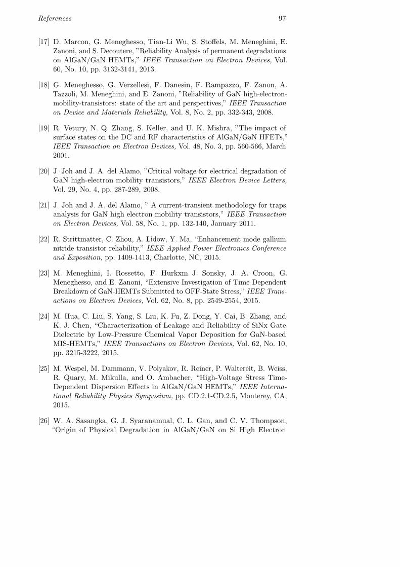
References 97
[17] D. Marcon, G. Meneghesso, Tian-Li Wu, S. Stoffels, M. Meneghini, E.Zanoni, and S. Decoutere, ”Reliability Analysis of permanent degradationson AlGaN/GaN HEMTs,” IEEE Transaction on Electron Devices, Vol.60, No. 10, pp. 3132-3141, 2013.
[18] G. Meneghesso, G. Verzellesi, F. Danesin, F. Rampazzo, F. Zanon, A.Tazzoli, M. Meneghini, and E. Zanoni, ”Reliability of GaN high-electron-mobility-transistors: state of the art and perspectives,” IEEE Transactionon Device and Materials Reliability, Vol. 8, No. 2, pp. 332-343, 2008.
[19] R. Vetury, N. Q. Zhang, S. Keller, and U. K. Mishra, ”The impact ofsurface states on the DC and RF characteristics of AlGaN/GaN HFETs,”IEEE Transaction on Electron Devices, Vol. 48, No. 3, pp. 560-566, March2001.
[20] J. Joh and J. A. del Alamo, ”Critical voltage for electrical degradation ofGaN high-electron mobility transistors,” IEEE Electron Device Letters,Vol. 29, No. 4, pp. 287-289, 2008.
[21] J. Joh and J. A. del Alamo, ” A current-transient methodology for trapsanalysis for GaN high electron mobility transistors,” IEEE Transactionon Electron Devices, Vol. 58, No. 1, pp. 132-140, January 2011.
[22] R. Strittmatter, C. Zhou, A. Lidow, Y. Ma, “Enhancement mode galliumnitride transistor reliability,” IEEE Applied Power Electronics Conferenceand Exposition, pp. 1409-1413, Charlotte, NC, 2015.
[23] M. Meneghini, I. Rossetto, F. Hurkxm J. Sonsky, J. A. Croon, G.Meneghesso, and E. Zanoni, “Extensive Investigation of Time-DependentBreakdown of GaN-HEMTs Submitted to OFF-State Stress,” IEEE Trans-actions on Electron Devices, Vol. 62, No. 8, pp. 2549-2554, 2015.
[24] M. Hua, C. Liu, S. Yang, S. Liu, K. Fu, Z. Dong, Y. Cai, B. Zhang, andK. J. Chen, “Characterization of Leakage and Reliability of SiNx GateDielectric by Low-Pressure Chemical Vapor Deposition for GaN-basedMIS-HEMTs,” IEEE Transactions on Electron Devices, Vol. 62, No. 10,pp. 3215-3222, 2015.
[25] M. Wespel, M. Dammann, V. Polyakov, R. Reiner, P. Waltereit, B. Weiss,R. Quary, M. Mikulla, and O. Ambacher, “High-Voltage Stress Time-Dependent Dispersion Effects in AlGaN/GaN HEMTs,” IEEE Interna-tional Reliability Physics Symposium, pp. CD.2.1-CD.2.5, Monterey, CA,2015.
[26] W. A. Sasangka, G. J. Syaranamual, C. L. Gan, and C. V. Thompson,“Origin of Physical Degradation in AlGaN/GaN on Si High Electron

98 References
Mobility Transistors under Reverse Bias Stressing,” IEEE InternationalReliability Physics Symposium, pp. 6C.3.1-6C.3.4, Monterey, CA, 2015.
[27] S. C. Liu, G. M. Dai, and E. Y. Chang, “Improved Reliability of GaNHEMTs Using N2 Plasma Surface Treatment,” IEEE International Sym-posium Physical and Failure Analysis of Integrated Circuits, pp. 378-380,Hsinchu, 2015.
[28] M. Florovic, J. Kovac, P. Benko, A. Chvala, J. Skriniarova, P. Kordo,”Electrical properties of recessed AlGaN/GaN Schottky diodes under off-state stress,” Journal of Electrical Engineering, Vol. 65, No. 5, pp. 313-316,2014.
[29] J. Hu, S. Stoffels, S. Lenci, N. Ronchi, R. Venegas, S. You, B. Bakeroot, G.Groeseneken, S. Decoutere, ”Physical origin of current collapse in Au-freeAlGaN/GaN Schottky barrier diodes,” Microelectronics Reliability, Vol.54, Nos. 9-10, pp. 2196-2199, 2014.
[30] J. A. Croon, G. A. M. Hurkx, and J. J. T. M. Donkers, ”Impact of thebackside potential on the current collapse of GaN SBDs and HEMTs,”IEEE International Symposium on Power Semiconductor Devices & IC’s,pp. 365-368, Hong Kong, 2015.
[31] H. Kang, Q. Wang, H. Xiao, C. Wang, L. Jiang, C. Feng, H. Chen, H. Yin,S. Qu, E. Peng, J. Gong, X. Wang, B. Li, Z. Wang, and X. Hou, ”Effectsof a GaN cap layer on the reliability of AlGaN/GaN Schottky diodes,”Physica Status Solidi A, Vol. 212, No. 5, pp. 1158-1161, 2015.
[32] J. Hu, S. Stoffels, S. Lenci, B. Bakeroot, R. Venegas, G. Groeseneken,and S. Decoutere, “Current transient spectroscopy for trapping analysison Au-free AlGaN/GaN Schottky barrier diode,” Applied Physics Letters,Vol. 106, No. 8, pp. 08350.21-24, 2015.
[33] A. Urtasun, P. Sanchis, and L. Marroyo, “Adaptive voltage control of theDC/DC boost stage in PV converters with small input capacitor,” IEEETransactions on Power Electronics, Vol. 28, No. 11, pp. 5038–5048, 2013.
[34] J. M. Alonso, D. Gacio, F. Sichirollo, A. R. Seidel, and M. A. Dalla Costa,“A straightforward methodology to modeling high power factor AC-DCconverters,” IEEE Transactions on Power Electronics, Vol. 28, No. 10, pp.4723–4731, 2013.
[35] A. Kulkarni and V. John, “Mitigation of lower order harmonics in agrid-connected single-phase PV inverter,” IEEE Transactions on PowerElectronics, Vol. 28, Vo. 11, pp. 5024–5037, 2013.

References 99
[36] A. Lahyani, P. Venet, A. Guermazi, and A. Troudi, “Battery/ Super-capacitors combination in uninterruptible power supply (UPS),” IEEETransactions on Power Electronics, Vol. 28, No. 4, pp. 1509–1522, 2013.
[37] R. Mitova, R. Ghosh, U. Mhaskar, D. Klikic, M. X. Wang, and A. Dentella,“Investigations of 600-V GaN HEMT and GaN Diode for Power ConverterApplications,” IEEE Transactions on Power Electronics, Vol. 29, No. 5,pp. 2441-2452, 2014.
[38] A. Terano, T. Tsuchiya and K. Mochizuki, “Investigation of relation-ship between 2DEG density and reverse leakage current in AlGaN/GaNSchottky barrier diodes,” Electronics Letters, Vol. 48, No. 5, pp. 274-275,2012.
[39] H. Zhang, E. J. Miller, and E. T. Yu, “Analysis of leakage current mech-anism in Schottky contacts to GaN and Al0.25Ga0.75N/GaN grown bymolecular-beam epitaxy,” Journal of Applied Physics, Vol. 99, No. 2, pp.0.23703-1-6, 2006.
[40] Sentaurus-Device U.G. v. J-2014.09, Synopsys Inc., 2014.
[41] D. Bisi, M. Meneghini, C. de Santi, A. Chini, M. Dammann, P. Bruckner,M. Mikulla, G. Meneghesso, and E. Zanoni, “Deep-level characterization inGaN HEMTs-part I: Advantages and limitations of drain current transientmeasurements,” IEEE Transaction on Electron Devices, Vol. 60, No. 10,pp. 3166-3175, 2013.
[42] D. K. Schroder, “Semiconductor material and device characterization,”Third Edition, Arizona State University Tempe, AZ, 2006.
Chapter 5
Gate Reliability of p-GaN powerHEMTs
5.1 Introduction and State of the Art
Recently, GaN-based power transistors have received great attention in powerelectronics applications, due to the advantages of GaN over the conventionalsilicon [1] and to the possibility of manufacturing these devices at a comparablecost than their aging Si-based competitors [2]. In particular, the increasingdemand for power switching applications, requiring normally-off devices forsafety, power consumption and cost reasons [3], pushes the interest in developingand manufacturing enhancement-mode GaN-on-Si power transistors.
In the last years, different approaches, designed to fabricate normally-offhigh electron mobility transistors (HEMTs), have been proposed:
• MIS- and MOS-HEMTs based on a deep barrier recess under the gateregion [4]-[10];
• fluorine plasma ion implantation into the AlGaN or GaN aimed atmodulating the local potential under the gate, thus depleting the twodimensional electron gas (2DEG) in the channel [11], [12];
• introducing a p-type gate (p-GaN or p-AlGaN) able to pull the conductionband of the gallium nitride (GaN) in the channel up and, consequently,opposing to the formation of the 2DEG [13]-[16].
According to a recent comparison of different enhancement-mode archi-tectures [17], the p-GaN solution seems to represent a promising technologybecause of the good trade-off between reliability and cost. In particular, byavoiding the deposition of an oxide/insulator layer (as in the case of MIS-/MOS-HEMT), the trapping-related degradation mechanisms (e.g. PBTI),caused by the defects at the GaN/insulator interface and/or in the bulk insu-lator, are strongly reduced [18]. Moreover, the adoption of standard silicon
100

5.2. Device Structure and Measurement Technique 101
manufacturing technology and facilities ensures a low process cost. However,relatively few data on trapping effects affecting the gate reliability of HEMTswith p-type gate are available in literature [19]-[21].
In [19] the breakdown phenomenon has been investigated and explained byavalanche multiplication in the space charge region of the Schottky metal/p-GaN junction, whereas in [20], the time dependence of the gate leakage currentdegradation was found to be consistent with a defect percolation process.Finally, Rossetto et al. [21], by combining experimental and simulation analyses,confirmed that the gate reliability of the p-GaN HEMTs is affected by thedegradation originated from the high electric field within the p-GaN layer.Moreover, it is suggested, without providing a specific model, that the initialgate leakage current and, thus, the initial defectiveness of the fresh deviceinfluence the time to failure.
In this chapter, the degradation mechanisms underneath the time-dependentbreakdown occurring when a forward constant voltage is applied on the p-typegate of the GaN-based transistor are extensively investigated. In particular,an original empirical relationship between gate leakage and time to failurethat guides device optimization is identified by means of extensive statisticalcharacterization on a few hundred devices. Moreover, thanks to this approachit has been found that:
• during the forward constant voltage stress a threshold voltage (VTH)degradation occurs;
• after the breakdown event, in addition to an increase of the gate leakage(IG), an improvement of the trans-conductance (gm) is noticeable;
• the increase of IG is ascribed to the creation of a percolation path in thedepletion region of the p-GaN layer (close to the metal interface), andthe possibly responsible defects are suggested;
• the VTH degradation is ascribed to defects located in the AlGaN barrierlayer;
• the gm improvement is correlated to the gate leakage increase and ascribedto the channel conductivity modulation in the region under the gate.
5.2 Device Structure and Measurement Technique
P-GaN gate HEMTs (Fig. 5.1), fabricated at imec using an Au-free CMOS-compatible process flow [22], with a nominal threshold voltage of ≈ 2.1 V, areconsidered in this study. The epitaxial structure, is grown on 8-inch <111>silicon substrate by means of MOCVD and features a stack of: 200 nm-thickAlN nucleation layer on top of the Si substrate, followed by 3000 nm-thick

102 Chapter 5. Gate Reliability of p-GaN power HEMTs
AlGaN buffer, 300 nm-thick GaN channel, 15 nm-thick Al25Ga75N barrier, 70nm-thick Mg-doped p−GaN , and 100 nm-thick TiN gate metal evaporated ontop of the p-GaN in order to form a Schottky contact able to reduce the gateleakage current. A selective etch of the p-GaN layer is performed in the accessregions stopping on the AlGaN layer and subsequently a SiN passivation layeris deposited. Finally, Au-free source and drain ohmic contacts are realized.The devices under test (DUT) feature a symmetric structure with a gate length(LG) of 0.8 µm, gate-source/drain spacing length (LGD = LGS) of 0.85 µm,and gate width of 500 µm.
On-wafer characterization has been performed by means of Keithley 26xxSource Measure Units. During the stress phase a constant voltage (VG) wasapplied on the gate contact while short-circuiting drain and source with thesubstrate. In this phase, the gate leakage current was continuously monitoreduntil reaching 1 mA/mm, the current level chosen to identify the breakdowncondition. Before and after the stress phase, a full IDVG transfer characteristicwas measured in order to monitor the gate leakage (IG), threshold voltage(VTH), drain-source resistance (RDS) and trans-conductance (gm). Finally, therecovery was monitored by applying 0 V on all device contacts and periodicallyanalyzing IG, VTH , RDS and gm.
Figure 5.1: Schematic of the p-GaN/AlGaN/GaN-on-Si HEMTs (not in scale).The AlN nucleation layer between the AlGaN buffer and the Si substrate, andthe SiN passivation layer are not shown.
5.3 Results and Discussion
Fig. 5.2 shows the gate current, monitored during the stress phase, of differentdevices biased with a gate voltage of 9.5 V at 25 ◦C. Two set of devices havebeen selected, characterized by different IG levels. By observing Fig. 5.2, itis possible to note that: i) the higher the initial gate leakage current (IG)(beginning of the stress), the shorter is the time to failure (TTF); ii) before thebreakdown event, a noisy phase is only exhibited by the devices featuring a

5.3. Results and Discussion 103
lower IG (set B in Fig. 5.2). In analogy to the case of CMOS FETs, this latterphenomenon may be ascribed to creation of defects forming a percolation path[23]-[26]. The higher initial gate leakage (set A in Fig. 5.2) can be related toa higher device defectiveness in fresh condition. As a result, with a highernumber of pre-existing defects (higher initial gate leakage) the formation of thepercolation path will only require the creation of a small number of additionaldefects and thus the noisy effect on the gate leakage is strongly reduced andTTF is significantly shorter. Larger defect creation, hence larger noisy behavior,occurs before breakdown in the case of devices featuring a low initial gateleakage (set B in Fig. 5.2).
10-3 10-2 10-1 100 101 102 103
10-9
10-8
10-7
10-6
10-5
10-4
A
Gat
e C
urre
nt (A
/mm
)
Stress Time (s)
VG = 9.5 VT = 25 C
B
Figure 5.2: Gate current monitored during the constant stress at VG = 9.5 Vand T = 25 ◦C. It is possible to note a correlation between initial gate leakagecurrent (IG) and time to failure (TTF). The higher is IG, the shorter is TTF.
The relationship between initial gate leakage (IG), monitored at the start ofthe stress, and time to failure (TTF) is shown in in Fig. 5.3. It is worth notingthat a statistical analysis has been performed in order to increase the accuracyof the analysis. In particular, for the case VG = 9.5 V, more than 150 deviceswithin a single wafer have been characterized at room temperature. Whilein [21] the stress gate voltage was modified in order to control gate current,in this case, in order to specifically highlight the link between TTF and IG,the analysis has been performed at fixed applied voltage for devices featuringdifferent levels of gate leakage.
The relationship between mean time to failure (MTTF) and initial IG iswell modeled by the exponential law reported in in Fig. 5.3. Moreover, thisdependence has been confirmed for different stress voltages (8.5, 9.0, and 9.5V). Thanks to this approach, the trade-off between safe operating gate voltagefor a given lifetime and leakage current, can be estimated.

104 Chapter 5. Gate Reliability of p-GaN power HEMTs
105 106 107 108 109 101010-1
100
101
102
103
104
105
106
MTTF = y0 + A eB / IG
VG = 9.5 V VG = 9.0 V VG = 8.5 V Exp. Fitting
Tim
e To
Fai
lure
(s)
1/IG (A/mm)-1
T = 25 C
Figure 5.3: Correlation between the gate leakage current (IG), monitored atthe beginning of the stress, and the time to failure. An empirical model hasbeen identified by means of a statistical analysis at room temperature andvalidated for three different stress conditions.
4 5 6 7 8 9 10
0,2
0,4
0,6
0,81
Linear
Power
VG = 7 VIG = 0.33 nA/mmIG = 0.34 nA/mmIG = 0.36 nA/mm
Gat
e C
urre
nt (n
A/m
m)
Gate Voltage (V)
Failure criterion:MTTF = 10 yearsT = 25 C
Exponential
Figure 5.4: Relationship between gate voltage and initial gate leakage estimatedby considering the empirical model of Fig. 5.3. In particular, by fixing themean time to failure (10 years) and extrapolating the initial gate leakage atthe corresponding gate voltage (Fig. 5.3), the maximum allowed initial IG andoperating voltage (VG) enforcing the lifetime specification can be estimated.
Fig. 5.4 reports the initial gate current versus stress voltage as extrapolatedfrom the exponential fits of the experimental data reported in in Fig. 5.3, bysetting a 10 years’ lifetime. In particular, based on the empirical model ofin Fig. 5.3, the values of y0, A and B parameters are extracted for each VGcondition. Then, the gate current (IG) corresponding to the desired mean time
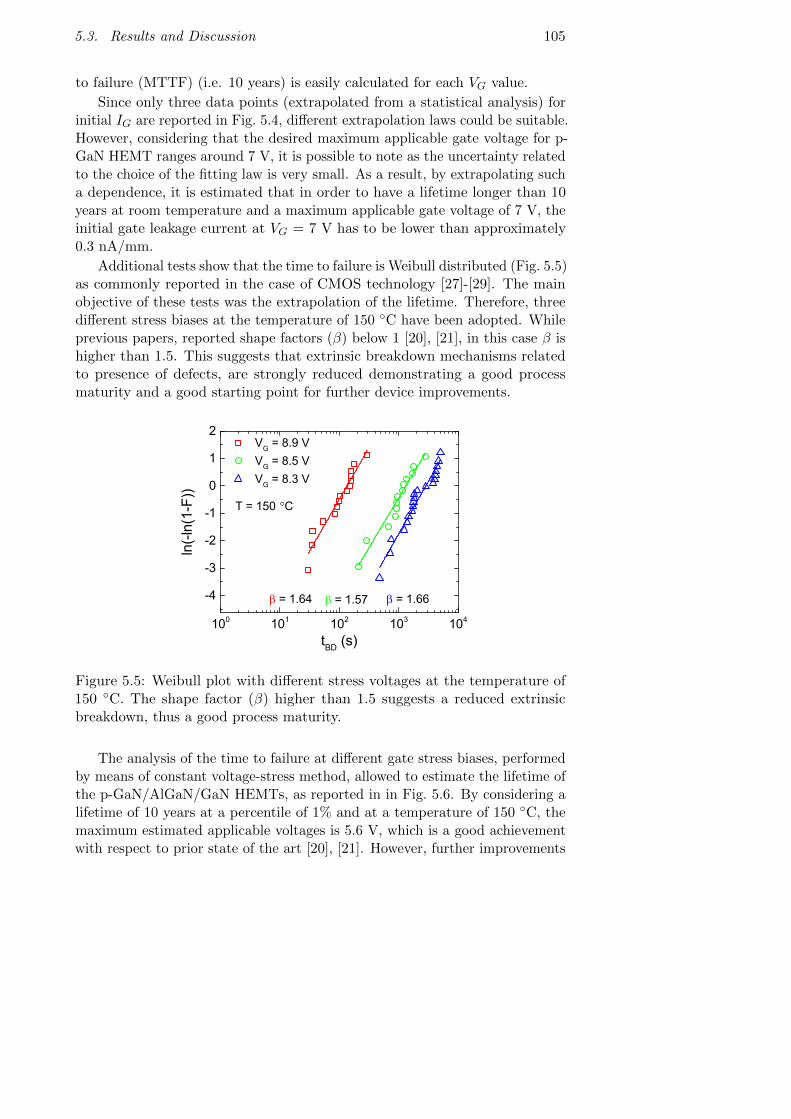
5.3. Results and Discussion 105
to failure (MTTF) (i.e. 10 years) is easily calculated for each VG value.
Since only three data points (extrapolated from a statistical analysis) forinitial IG are reported in Fig. 5.4, different extrapolation laws could be suitable.However, considering that the desired maximum applicable gate voltage for p-GaN HEMT ranges around 7 V, it is possible to note as the uncertainty relatedto the choice of the fitting law is very small. As a result, by extrapolating sucha dependence, it is estimated that in order to have a lifetime longer than 10years at room temperature and a maximum applicable gate voltage of 7 V, theinitial gate leakage current at VG = 7 V has to be lower than approximately0.3 nA/mm.
Additional tests show that the time to failure is Weibull distributed (Fig. 5.5)as commonly reported in the case of CMOS technology [27]-[29]. The mainobjective of these tests was the extrapolation of the lifetime. Therefore, threedifferent stress biases at the temperature of 150 ◦C have been adopted. Whileprevious papers, reported shape factors (β) below 1 [20], [21], in this case β ishigher than 1.5. This suggests that extrinsic breakdown mechanisms relatedto presence of defects, are strongly reduced demonstrating a good processmaturity and a good starting point for further device improvements.
100 101 102 103 104
-4
-3
-2
-1
0
1
2 VG = 8.9 V VG = 8.5 V VG = 8.3 V
ln(-l
n(1-
F))
tBD (s)
= 1.64 = 1.57 = 1.66
T = 150 C
Figure 5.5: Weibull plot with different stress voltages at the temperature of150 ◦C. The shape factor (β) higher than 1.5 suggests a reduced extrinsicbreakdown, thus a good process maturity.
The analysis of the time to failure at different gate stress biases, performedby means of constant voltage-stress method, allowed to estimate the lifetime ofthe p-GaN/AlGaN/GaN HEMTs, as reported in in Fig. 5.6. By considering alifetime of 10 years at a percentile of 1% and at a temperature of 150 ◦C, themaximum estimated applicable voltages is 5.6 V, which is a good achievementwith respect to prior state of the art [20], [21]. However, further improvements

106 Chapter 5. Gate Reliability of p-GaN power HEMTs
are needed in order to achieve this device reliability for large area devices.
0 1 2 3 4 5 6 7 8 9 10100101102103104105106107108109
1010
VMAX = 5.6 V
Life
time
(s)
Gate Voltage (V)
10 years
Failure criterion:F = 1 %T = 150 C
Exponential law
Figure 5.6: Lifetime extrapolation. By choosing the 1% of failure rate in10 years at the temperature of 150 ◦C, the maximum applicable voltage,considering a device gate area of 400 µm2, is 5.6 V. This is a good achievementconsidering the present state of the art. However, further improvements arerequired in order to have similar reliability for larger gate areas.
DC characterization has been performed before and after the gate failureaiming at monitoring and then at comparing the performance of the fresh anddegraded samples. The transfer characteristics and the gate leakage current,in fresh and after the breakdown conditions, are reported in Fig. 5.7a and5.7b, respectively. It is worth noting that Fig. 5.7 reports the results for arepresentative device. However, the same behavior has been observed for alltested devices.
By focusing on the curves measured after the breakdown and reported inFig. 5.7 (red curves), it is possible to notice: i) an increase of the gate leakagecurrent (b), ii) an improvement of the transconductance (gm) (a); iii) a goodcorrelation between the increase of gm and IG (a and b).
The gate leakage increase and hence the breakdown phenomenon may berelated to the creation of a percolation path occurring in the depletion regionof the p-GaN region of the Schottky junction, where the highest electric fieldoccurs for positive gate bias. In order to confirm this hypothesis, the equivalentcircuit of the p-GaN gate (Fig. 5.8a) may be considered. It consists of two backto back connected junctions. A Schottky diode formed by metal (TiN)/p-GaN(D1) and a PiN diode formed by p-GaN/AlGaN/GaN (D2). As a result, whena positive bias is applied on the gate, the diodes D1 and D2 are inversely anddirectly biased, respectively. Consequently, for high gate voltages the leakagecurrent is limited by the Schottky diode (D1). This is supported by the voltage

5.3. Results and Discussion 107
drops across the diodes D1 and D2, evaluated analytically for a representativedevice by setting the reverse current of D1 and forward current of D2 equal toexperimental gate leakage current [30], and reported in Fig. 5.8b.
0
1
2
3
4
5
6
(b)
(a)
I DS (
mA/
mm
) fresh after_BD
VDS = 50 mVT = 150 C
0,0 0,5 1,0 1,5 2,0 2,5 3,0 3,5 4,0
10-12
10-10
10-8
10-6
10-4
High hole injection regime
I G (A
/mm
)
Gate Voltage (V)
Low hole injectionregime
Figure 5.7: Transfer characteristics (a) and gate leakage currents (b) monitoredin fresh devices and just after the breakdown event. After the failure it ispossible to note an increase of IG (b) due to creation of the percolation pathin depletion region of the p-GaN layer and an improvement of gm (a) linked toconductivity modulation mechanism triggered by high hole injection.
For VG higher than ≈ 1.5 V the voltage drop across the AlGaN barrier (D2)is almost saturated and the whole additional applied gate voltage drops acrossthe depletion region of the p-GaN layer (D1). As a result, defects induced byhigh fields form a percolation path in this latter region, leading to an increaseof the gate leakage current (Fig. 5.7b).
By observing Fig. 5.7a, it is possible to note an improvement of the transcon-ductance occurring after the breakdown event (circle/red curve). Moreover, acorrelation with the increase of IG (Fig. 5.7b) exists. According to [31], this canbe ascribed to a conductivity modulation phenomenon. In [31] a GaN-basedHEMT featuring a gate ohmic contact instead of a Schottky one is considered.

108 Chapter 5. Gate Reliability of p-GaN power HEMTs
0 1 2 3 4 5 6 7 8 9 100123456789
10
D2
D1
(b)Al
GaN
dom
inat
ed
Volta
ge d
rop
acro
ss S
chot
tky
(V)
VG (V)
Schottky dominated
012345678910
Volta
ge d
rop
acro
ss A
lGaN
(V)
Figure 5.8: Schematic of the p-GaN gate (a) and evaluated diodes voltagedrop (b). When a positive bias is applied on the gate, the diode D1 (Schottky)is in reversely biased, sustaining a high voltage and blocking reverse current,whereas the diode D2 (PiN) is in forward operation mode.
This new device principle utilizes hole-injection from the p-AlGaN tothe AlGaN/GaN heterojunction, which simultaneously increases the electrondensity in the channel, resulting in a dramatic increase of the drain currentowing to the associated conductivity modulation. In the case analyzed inthis work, after the local Schottky barrier collapse caused by the opening ofa percolation path, a similar mechanism occurs. In particular, it is thoughtthat after the percolation path is activated, hole concentration increases inthe AlGaN barrier. These holes can neutralize magnesium ions in the AlGaNbarrier (Fig. 5.9b) increasing the 2DEG density in the channel. Notice that,the holes tunneling through or jumping above the AlGaN barrier, differentlyfrom electrons, are not confined at the AlGaN/GaN interface (Fig. 5.9b).The modulation of electron concentration by unconfined excess-hole tends tobroaden the quantum well of the 2DEG, increasing its sheet concentration. Asa result, the combined effect of neutralized magnesium ions into the AlGaNand the conductivity modulation induced by the holes injected in the channelreduces the channel resistance.

5.3. Results and Discussion 109
Figure 5.9: Band diagrams, considered under the gate region, in the case oflow (a) (no percolation path) and high hole injection regime (b) (percolationpath). The combined effect of magnesium ions neutralization in the AlGaNdue to high hole injection, and the lack of hole confinement in the channel (b)can reduce the sheet resistance of the 2DEG improving gm.
Additional understanding in the degradation physics was gained by imple-menting a percolation model in TCAD. The percolation path was implementedas a highly p-doped region, in accordance with the models which Uren etal. are using for their buffer simulations [32]. The simulation of the holeconcentration with and without the percolation path are shown in Fig. 5.10.In the presence of a percolation path, a significant hole injection occurs intothe channel where being unconfined causes a widening of the 2DEG quantumwell, thus decreasing the 2DEG resistance. The depletion region below the2DEG is indicated by a white line and is clearly extended towards the bottomfor the case with percolation path. The simulated curves reported in Fig. 5.11are qualitatively similar to the experimental curves of Fig. 5.7.

110 Chapter 5. Gate Reliability of p-GaN power HEMTs
Figure 5.10: TCAD simulation of a p-GaN gate with and without p-typepercolation path.
0
2
4
6
0 1 2 3 410-13
10-11
10-9
10-7
10-5
(b)
No Leakage path Leakage path
I DS (
mA)
(a)
I G (A
)
VG (V)
Figure 5.11: Simulated transfer characteristics (a) and gate leakage currents(b) monitored with and without p-type percolation path.

5.3. Results and Discussion 111
In order to further confirm the role played by trapping/detrapping mecha-nisms in the catastrophic gate failure, and the correlation between the gateleakage current and the transconductance, a recovery analysis has been per-formed and reported in Fig. 5.12. After the breakdown event, 0 V was appliedon gate, source and drain at the temperature of 150 ◦C in order to allow arecovery phase. Gate leakage and transconductance were periodically moni-tored by measuring a full IDVG transfer characteristic from 0 V to 4 V withVDS = 50 mV. By observing Fig. 5.12, the correlation between IG and gmis confirmed. It is thought that, during the recovery phase at T = 150 ◦C,some defect forming the percolation path are deactivated reducing the gateleakage (Fig. 5.12b). As a result, the smaller the hole injection, the smallerthe conductivity modulation mechanism affecting the 2DEG resistance underthe gate.
0
1
2
3
4
5
6
(b)
(a)tR 6 h
I DS (
mA/
mm
)
fresh after_BD recovered
VDS = 50 mVT = 150 C
Recovery cond. VG = VD = VS = 0 VT = 150 C
tR 0 s
0,0 0,5 1,0 1,5 2,0 2,5 3,0 3,5 4,0
10-12
10-10
10-8
10-6
10-4
Total IG and RDS recovery after 6 h
I G (A
/mm
)
Gate Voltage (V)
Figure 5.12: Transfer characteristics (a) and gate leakage currents (b) monitoredin fresh condition, after the breakdown event, and during the recovery phase.In this latter, 0 V was applied on all device contacts at T = 150 ◦C. Thecorrelation between gm (a) and IG (b) is further proved. It is worth notingthat as in the case of Fig. 5.7 and 5.13, only a representative device is shown,but same behavior is reproducible for all tested devices.
However, although after ≈ 6 hours the gate leakage shows a complete

112 Chapter 5. Gate Reliability of p-GaN power HEMTs
recovery for VG up to 4 V, a permanent or slowly recoverable damage can beobserved in Fig. 5.13. In particular, after a recovery of ≈ 22 hours at T = 150◦C, it is possible to note that the breakdown voltage of the recovered device(green) is lower than that of the fresh device (6 V and 10.5 V, respectively). Asa result, part of the defects created during the stress and deactivated duringthe recovery can be easily re-activated when a high voltage is applied on thegate.
0 1 2 3 4 5 6 7 8 9 10 11 1210-1310-1210-1110-1010-910-810-710-610-510-410-310-210-1
permanentdamage
I G (A
/mm
)
Gate Voltage [V]
fresh after_BD after recovery
T = 150 C
Figure 5.13: Device breakdown voltage characterized in fresh condition (blue),after the breakdown (red), and after 22 hours of recovery at T = 150 ◦C (green).Despite the full recovery shown for low voltage in Fig. 5.12, a permanentor slowly recoverable damage affects the device after the breakdown (VBDrecovered < VBD fresh).
Finally, a temperature-dependent analysis aimed at understanding thepossible kind of defects behind the trapping/detrapping mechanisms has beenperformed. In particular, by investigating the temperature dependence of theTTF, the nature of the defects located in the p-GaN layer can be identified.It is worth noting that each data reported in Fig. 5.14 is representative ofthe average of ≈ 20 samples stressed at a given temperature. In order toaccount for the statistics dispersion due to device variability, the error barswere calculated as ± 3σ (σ = standard deviation).
The temperature dependence of the time to failure is reported in Fig. 5.14.From the Arrhenius plot an activation energy of 0.44 eV is estimated. Byconsidering the database of the deep levels in GaN- and AlGaN-based devices(see [33]), traps having an activation energy of 0.44 eV can be related to oxygenimpurities in the gallium nitride [34], meaning that for our structure thesedefects would be present in the p-GaN gate.

5.4. Conclusions 113
25 30 35 4010-1
100
101
102
103
104
VG = 9.0 V
Mea
n Ti
me
To F
ailu
re (s
)
1/kT (eV-1)
Fitting: MTTF = A exp(Ea/kT)
Ea = 0.44 eV
Error bar =
Figure 5.14: Arrhenius plot considering the mean time to failure (MTTF). TheTTF has been extrapolated at the gate current of 1 mA/mm. By consideringthe database of the deep levels in GaN- and AlGaN-based devices [33, 34], theactivation energy of ≈ 0.44 eV can be linked to the oxygen impurities in thegallium nitride.
5.4 Conclusions
In this chapter, the failure mechanisms induced by constant-voltage forwardgate stress in GaN-on-Si power HEMTs with p-type gate have been investigated.
In particular, based on a statistical analysis, it has been found the following:
• the time to failure follows a Weibull distribution and it is function of theinitial gate leakage. The higher is the gate leakage, the shorter is thetime to failure. An empirical exponential model was proposed to takeinto account for this dependence;
• a maximum gate voltage of 5.6 V was estimated to ensure a 10 years’lifetime at a percentile of 1% and 150 ◦C;
• the breakdown mechanism is ascribed to the creation of the percolationpath in the p-GaN layer (close the metal interface). When a high positivebias is applied on the gate, a large electric field (voltage drop) occurs inthe depletion region of the p-GaN, creating defects with an activationenergy of 0.44 eV;
• finally, the high hole injection occurring after the local Schottky barriercollapse, improves the transconductance due to a conductivity modula-tion phenomenon. In particular, the combined effect of the magnesiumneutralization in the AlGaN barrier and the increase of hole concentration

114 Chapter 5. Gate Reliability of p-GaN power HEMTs
in the channel, contribute to increase the 2DEG density and the mobilityunder the gate;

References
[1] A. Lidow, J. Strydom, M. de Rooij, D. Reusch, “GaN Transistors forEfficient Power Conversion,” Second Edition, John Wiley and Sons, Aug.2014, ISBN: 978-1-118-84476-2.
[2] A. Lidow, “GaN-Transistors – Giving New Life to Moore’s Law,” IEEEInternational Symposium on Power Semiconductor Devices & IC’s, pp.1-6, Hong Kong, May 2015.
[3] J. Millan, P. Godignon, X. Perpina, A. Perez-Tomas, and J. Rebollo, “Asurvey of wide bandgap power semiconductor devices,” IEEE Transactionson Power Electronics, Vol. 29, No. 5, pp. 2155–2163, May 2014.
[4] T. Imada, M. Kanamura, T. Kikkawa, “Enhancement-mode GaN MIS-HEMTs for power supplies,” IEEE International Power Electronics Con-ference, pp. 1027-1033, Sapporo, Jun. 2010.
[5] S.C. Lie, B.Y. Chen, Y.C. Lin, T.E. Hsieh, H.C. Wang, and E.Y. Chang,“GaN MIS-HEMTs with nitrogen passivation for power device applications,”IEEE Electron Device Letters, Vol. 35, No. 10, pp. 1001-1003, Oct. 2014.
[6] M. Kanamura, T. Ohki, T. Kikkawa, K. Imanishi, T. Imada, A. Yamada,and N. Hara, “Enhancement-mode GaN MIS-HEMTs with n-GaN/i-AlN/n-GaN triple cap layer and high-k gate dielectrics,” IEEE ElectronDevice Letters, Vol. 31, No. 3, pp. 189-191, Mar. 2010.
[7] Y. Shi, S. Huang, Q. Bao, X. Wang, K. Wei, H. Jiang, J. Li, C. Zhao, S.Li, Y. Zhou, H. Gao, Q. Sun, H. Yang, J. Zhang, W. Chen, Q. Zhou, B.Zhang, and X. Liu, “Normally OFF GaN-on-Si MIS-HEMTs fabricatedwith LPCVD-SiNx passivation and high-temperature gate recess,” IEEETransaction on Electron Devices, Vol. 63. No. 2, pp. 614-619, Feb. 2016.
[8] J. Wei, S. Liu, B. Li, X. Tang, Y. Lu, C. Liu, M. Hua, Z. Zhang, G.Tang, and K. J. Chen, “Enhancement-mode GaN double-channel MOS-HEMT with low on-resistance and robust gate recess,” IEEE InternationalElectron Devices Meeting, pp. 9.4.1-9.4.4, Washington, DC, Dec. 2015.
115

116 References
[9] C. Tang, G. Xie, and K. Sheng, “Enhancement-mode GaN-on-Silicon MOS-HEMT using pure wet etch technique,” IEEE International Symposiumon Power Semiconductor Devices & IC’s, pp. 233-236, Hong Kong, May2015.
[10] J. Wu, W. Lu, P. K. L. Yu, “Normally-OFF AlGaN/GaN MOS-HEMTwith a two-step gate recess,” IEEE International Conference on ElectronDevices and Solid-State Circuits, pp. 594-596, Singapore, Jun. 2015.
[11] K. J. Chen, L. Yuan, M. J. Wang, H. Chen, S. Huang, Q. Zhou, C. Zhou,B. K. Li, J. N. Wang, “Physics of fluorine plasma ion implantation for GaNnormally-off HEMT technology,” IEEE International Electron DevicesMeeting, pp. 19.4.1-19.4.4, Washington, DC, Dec. 2011.
[12] S. Hamady, F. Morancho, B. Beydoun, P. Austin, M. Gavelle, “A newconcept of enhanced-mode GaN HEMT using fluorine implantation inthe GaN layer,” IEEE European Conference on Power Electronics andApplications, pp. 1-6, Lille, Sept. 2013.
[13] I. Hwang, H. Choi, J. W. Lee, H. S. Choi, J. Kim, J. Ha, C. Y. Um, S. K.Hwang, J. Oh, J. Y. Kim, J. K. Shin, Y. Park, U. Chung, I.K. Yoo, andK. Kim., “1.6 kV, 2.9 mω cm2 normally-off p-GaN HEMT device,” IEEEInternational Symposium on Power Semiconductor Devices & IC’s, pp.41-44, Bruges, Jun. 2012.
[14] E. V. Erofeev, V.A. Kagadei, A. I. Kazimmirov, I. V. Fedin, “High thresh-old voltage p-gate GaN transistors,” International Siberian Conference onControl and Communications, pp. 1-4, Omsk, May 2015.
[15] O. Hilt, F. Brunner, E. Cho, A. Knauer, E. Bahat-Treidel, and J. Wurfl,“Normally-off High-Voltage p-GaN Gate GaN HFET with Carbon-DopedBuffer,” IEEE International Symposium on Power Semiconductor Devices& IC’s, pp. 239-242, San Diego, May 2011.
[16] Y. Uemoto, M. Hikita, H. Ueno, H. Matsuo, H. Ishida, M. Yanagihara,T. Ueda, T. Tanaka, and D. Ueda, “Gate Injection Transistor (GIT)—ANormally-Off AlGaN/GaN Power Transistor Using Conductivity Mod-ulation,” IEEE Transactions on Electron Devices, Vol. 54, No. 12, pp.3393-3399, Dec. 2007.
[17] D. Marcon, Y. N. Saripalli, S. Decoutere, “200mm GaN-on-Si epitaxy ande-mode device technology,” IEEE International Electron Devices Meeting,pp. 16.2.1-16.2.4, Washington, DC, Dec. 2015.
[18] F. Crupi, P. Magnone, S. Strangio, F. Iucolano, and G. Meneghesso, “LowFrequency Noise and Gate Bias Instability in Normally-OFF AlGaN/GaN

References 117
HEMTs,” IEEE Transactions on Electron Devices, Vol. 63, No. 5, pp.2219-2222, May 2016.
[19] T. L. Wu, D. Marcon, S. You, N. Posthuma, B. Bakeroot, S. Stoffels, M. V.Hove, G. Groeseneken, and S. Decoutere, “Forward bias gate breakdownmechanism in enhancement-mode p-GaN gate AlGaN/GaN high-electronmobility transistors,” IEEE Electron Device Letters, Vol. 36, No. 10, pp.1001-1003, Oct. 2015.
[20] M. Tapajina, O. Hilt, E. B. Treidel, J. Wurfl, and J. Kuzmik, “GateReliability Investigation in Normally-Off p-Type-GaN Cap/AlGaN/GaNHEMTs Under Forward Bias Stress,” IEEE Electron Device Letters, Vol.37, No. 4, Apr. 2016.
[21] I. Rossetto, M. Meneghini, O. Hilt, E. B. Treidel, C. De Santi, S. Dalcanale,J. Wuerfl, E. Zanoni, and G. Meneghesso, “Time-Dependent Failure ofGaN-on-Si Power HEMTs with p-GaN Gate,” IEEE Transactions onElectron Devices, Vol. 63, No. 6, pp. 2334-2339, Jun. 2016.
[22] N. E. Posthuma et al,” IEEE International Symposium on Power Semi-conductor Devices & IC’s, pp. 95-98, Prague, Jun. 2016.
[23] T Fenfen, Y. Hong, T. Bo, T. Zhaoyun, X. Yefeng, X. Jing, W. Qingpu,and Y. Jiang, “TDDB characteristic and breakdown mechanism of ultra-thin SiO2/HfO2 bilayer gate dielectric,” Journal of Semiconductor, Vol.35, No. 6, pp. 064003-1-064003-6, 2014.
[24] A. Cester, L. Bandiera, G Ghidini, I. Bloom, A. Paccagnella, “Soft break-down current noise in ultra-thin gate oxides,” Solid-State Electronics, Vol.46, No. 7, pp. 1019-1025, Jul. 2002.
[25] B. E. Weir, P. J. Silverman, D. Monroe, K. S. Krisch, M. A. Alam, G. B.Alers, T. W. Sorsch, G. L. Timp, F. Baumann, C. T. Liu, Y. Ma, D. Hwang,“Ultra-thin gate dielectrics: they break down, but do they failure?,” IEEEInternational Electron Devices Meeting, pp. 73-76, Washington, DC, USA,Dec. 1997.
[26] Y. H. Kim, J. C. Lee, “Reliability characteristics of high-k dielectrics,”Microelectronics Reliability, Vol. 44, No. 2, pp. 183-193, Feb. 2004.
[27] R. Degraeve, G. Groeseneken, R. Bellens, M. Depas, H. E. Maes, “Aconsistent model for the thickness dependence of intrinsic breakdownin ultra-thin oxides,” IEEE International Electron Devices Meeting, pp.863-866, Washington, DC, Dec. 1995.
[28] K. Yamabe, K. Taniguchi, “Time-dependent-dielectric breakdown of thinthermally grown SiO2films,” IEEE Transactions on Electron Devices, Vol.32. No. 2, pp. 423-428, Feb. 1985.
118 References
[29] Y. H. Kim, K. Onishi, C. S. Kang, H. J. Cho, S. Krishnan, M. S. Akbar, J.C. Lee, “Thickness dependence of Weibull slopes of HfO2 gate dielectrics,”IEEE Electron Device Letters, Vol. 24, No. 1, pp. 40-42, Jan. 2003.
[30] S. Stoffels, A. N. Tallarico, B. Bakeroot, T.L. Wu, D. Marcon, N. E.Posthuma, C. Fiegna, S. Decoutere, “Failure Mode for p-GaN gates underforward gate stress with varying Mg concentration,” IEEE InternationalReliability Physics Symposium (IRPS), accepted, Monterey, CA, Apr.2017.
[31] Y. Uemoto, M. Hikita, H. Ueno, H. Matsuo, H. Ishida, M. Yanagihara,T. Ueda, T. Tanaka, and D. Ueda, “Gate Injection Transistor (GIT)—ANormally-Off AlGaN/GaN Power Transistor Using Conductivity Mod-ulation,” IEEE Transactions on Electron Devices, Vol. 54, No. 12, pp.3393-3399, Dec. 2007.
[32] M J. Huren, M. Silvestri, M. Casar, G. A. M. Hurkx, J. A. Croon, J.Sonsky, M. Kuball, ”Intentionally Carbon-Doped AlGaN/GaN HEMTsNecessity for Vertical Leakage Paths,” IEEE Electron Device Letters, Vol.35, No. 3, pp. 327-329, Mar. 2014.
[33] D. Bisi, M. Meneghini, C. de Santi, A. Chini, M. Dammann, P. Bruckner,M. Mikulla, G. Meneghesso, and E. Zanoni, “Deep-level characterization inGaN HEMTs-part I: Advantages and limitations of drain current transientmeasurements,” IEEE Transaction on Electron Devices, Vol. 60, No. 10,pp. 3166-3175, Oct. 2013.
[34] M. Caesar, M. Dammann, V. Polyakov, P. Waltereit, W. Bronner, M.Baeumler, R. Quay, M. Mikulla, and O. Ambacher, “Generation of traps inAlGaN/GaN HEMTs during RF-and DC-stress test,” IEEE InternationalReliability Physics Symposium, pp. CD.6.1–CD.6.5, Anaheim, CA, Apr.2012.

Chapter 6
Conclusions
With the evolving of power electronics applications, there is an increasing needto fabricate switching mode semiconductor power devices that are compact,cheap and evermore efficient and reliable. This last feature is one of the mainissues for power devices because it forces a trade-off between long lifetime,high performance and low cost. Consequently, extensive investigation and deepunderstanding of reliability issues are strongly required in order to keep upwith the fast evolution of power electronics.
Chapter 1 presented the wide range of applications in which switching-modepower devices can be adopted, and analyzed the typical operating regimesrepresenting the most critical conditions affecting the power device reliability,i.e. OFF-state, ON-state and SEMI ON-state.
This thesis aimed at studying, characterizing and modeling the trappingand de-trapping mechanisms, underneath the semiconductor power devicesdegradation, occurring during the ON-state operation mode. Although ON-state degradation received much less attention so far compared to OFF-statecase, as demonstrated in this thesis, its impact on the power devices reliabilityis significant. This investigation has been carried out on technologies basedon different semiconductors such as silicon and gallium nitride and differentdevices such as transistors and Schottky diodes, by means of accelerated life testmethods combined with electro-thermal simulations, aimed at understandingthe physical origins of the degradation.
The effects of degradation induced by Negative Bias Temperature Instabilityhave been investigated in p-channel Si-based power U-MOSFETs, becausethis degradation mechanism appears as the most critical one occurring whentransistor is in ON-state. Because of its vertical structure, moderate transverseelectric fields and impact ionization related effects occur in the drift region. Thislatter, being far from the channel and hence from silicon/oxide interface, leadsto negligible trapping mechanisms. On the other hand, the high/moderate gatebias required for ensuring a high drain current combined to a high temperaturedue to self-heating effects, causes thermally activated trapping mechanisms (i.e.
119

120 Chapter 6. Conclusions
NBTI) in the gate region, affecting the device reliability. The contributions ofthe interface and bulk traps and their role on the degradation and recoverydynamics of the main figures of merit, have been analyzed and discussed. Inparticular, both oxide charge trapping and interface state generation occurduring the stress, causing a degradation of threshold voltage and sub-thresholdslope. On the other hand, the recovery mechanism is mainly dominated bycharge de-trapping from bulk oxide defects featuring an energy confined in thesilicon bandgap (between 0.22 eV and 0.84 eV from silicon valence band) anda distance from SiO2/Si interface ranging between 2.24 and 3.04 nm.
Degradation mechanisms induced by ON-state stress have been also investi-gated in GaN-based Schottky barrier diodes (SBDs) and high electron mobilitytransistors (HEMTs). During ON-state stress, both devices are subject to highcurrent levels, hence self-heating effects play an important role on the deviceperformance and reliability limitations. Unfortunately, being GaN-based de-vices grown on foreign substrates with different thermal expansions coefficientsand large lattice mismatch, an additional transition layer aimed at avoiding theformation of cracks in the GaN heterostructure is needed. This latter, in addi-tion to structure vertical breakdown issues, implies a temperature increase dueto the low thermal conductivity of the transition layer stack. In order to modelthis effect, a physical model accounting for the temperature dependence of thethermal boundary resistance (TBR) associated to the transition stack, has beenimplemented in the Sentaurus TCAD simulator in order to realistically modelself-heating effects. In particular, it has been shown that, not including theTBR contributions, leads to an underestimation of the device channel/junctiontemperature by 25/30 %, resulting in an inaccurate estimation of the deviceperformance and reliability.
A combined experimental/simulation analysis has been performed in orderto understand the degradation induced in GaN-based Schottky barrier diodes(SBDs) by the combined effect of moderate electric fields and high temperatureduring ON-state stress. In particular, by analyzing the geometry dependenceof the device degradation it has been reported that: the turn-on voltagedegradation is linked to the vertical electric field under the Schottky junction,possibly activating nitrogen vacancies defects in the AlGaN barrier; the ON-resistance degradation is ascribed to longitudinal electric field occurring in theGaN channel, probably leading to the activation of nitrogen antisites defects;the RON starts to significantly degrade only when a critical temperature-dependent (longitudinal) electric field (or current level) is reached in the GaNchannel.
Finally, the time-dependent breakdown, induced by forward gate stress inGaN-based power HEMTs with p-type gate, has been analyzed because theintroduction of a p-type layer above the AlGaN barrier, aimed at realizing anenhancement-mode transistor, leads to undesired trapping mechanisms inducinga premature gate failure. The mechanisms underlying the gate breakdown

121
and its effects on the device performance have been investigated by adoptingdifferent stress conditions, analyzing the influence of the temperature, andinvestigating the activation energy of the traps. In particular, the breakdownmechanism has been ascribed to the creation of the percolation path in thep-GaN layer close the metal interface. When a high positive bias is applied onthe gate, a large electric field (voltage drop) occurs in the depletion region ofthe p-GaN, creating defects with an activation energy of 0.44 eV. Moreover, anoriginal empirical model, representing the relationship between gate leakagecurrent and time to failure, has been proposed.