alpha 21066 and alpha 21066a microprocessors datasheet · alpha 21066 and alpha 21066a...
TRANSCRIPT

Alpha 21066 and Alpha 21066AMicroprocessorsData SheetOrder Number: EC–QC4HB–TE
Revision/Update Information: This document supersedes theAlpha 21066/21066A MicroprocessorsData Sheet (EC–QC4HA–TE).
Digital Equipment CorporationMaynard, Massachusetts

December 1995
While Digital believes the information included in this publication is correct as of the date ofpublication, it is subject to change without notice.
Digital Equipment Corporation makes no representations that the use of its products in themanner described in this publication will not infringe on existing or future patent rights, nor dothe descriptions contained in this publication imply the granting of licenses to make, use, or sellequipment or software in accordance with the description.
© Digital Equipment Corporation 1995. All rights reserved.Printed in U.S.A.
AlphaGeneration, DECchip, Digital, Digital Semiconductor, VAX, VAX DOCUMENT, theAlphaGeneration design mark, and the DIGITAL logo are trademarks of Digital EquipmentCorporation.
Digital Semiconductor is a Digital Equipment Corporation business.
IEEE is a registered trademark of The Institute of Electrical and Electronic Engineers, Inc.GRAFOIL is a registered trademark of Union Carbide Corporation.
All other trademarks and registered trademarks are the property of their respective owners.
This document was prepared using VAX DOCUMENT Version 2.1.

Contents
1 Microarchitecture . . . . . . . . . . . . . . . . . . . . . . . . . . . . . . . . . . . . . 11.1 Overview . . . . . . . . . . . . . . . . . . . . . . . . . . . . . . . . . . . . . . . . 11.2 Instruction Fetch and Decode Unit . . . . . . . . . . . . . . . . . . . . 31.3 Integer Execution Unit . . . . . . . . . . . . . . . . . . . . . . . . . . . . . 51.4 Load and Store Unit . . . . . . . . . . . . . . . . . . . . . . . . . . . . . . . 51.5 Floating-Point Unit . . . . . . . . . . . . . . . . . . . . . . . . . . . . . . . . 71.6 Pipeline Organization . . . . . . . . . . . . . . . . . . . . . . . . . . . . . . 81.7 Internal Cache Organization . . . . . . . . . . . . . . . . . . . . . . . . . 91.8 Memory Controller . . . . . . . . . . . . . . . . . . . . . . . . . . . . . . . . . 91.9 I/O Controller . . . . . . . . . . . . . . . . . . . . . . . . . . . . . . . . . . . . . 101.10 Obtaining Additional Information . . . . . . . . . . . . . . . . . . . . . 102 Pinout . . . . . . . . . . . . . . . . . . . . . . . . . . . . . . . . . . . . . . . . . . . . . 112.1 Signal List . . . . . . . . . . . . . . . . . . . . . . . . . . . . . . . . . . . . . . . 112.2 Signal Descriptions . . . . . . . . . . . . . . . . . . . . . . . . . . . . . . . . 152.3 Quick Reference to Signals by Function and Direction . . . . . 233 Electrical Specifications . . . . . . . . . . . . . . . . . . . . . . . . . . . . . . . . 273.1 PCI Electrical Specification Conformance . . . . . . . . . . . . . . . 273.2 Absolute Maximum Ratings . . . . . . . . . . . . . . . . . . . . . . . . . . 273.3 Supply Current and Power Dissipation . . . . . . . . . . . . . . . . . 283.4 Chip Power Supply Sequencing . . . . . . . . . . . . . . . . . . . . . . . 293.5 dc Specifications . . . . . . . . . . . . . . . . . . . . . . . . . . . . . . . . . . . 303.5.1 dc Operating Specifications . . . . . . . . . . . . . . . . . . . . . . . 323.6 ac Specifications . . . . . . . . . . . . . . . . . . . . . . . . . . . . . . . . . . . 354 Mechanical Specifications . . . . . . . . . . . . . . . . . . . . . . . . . . . . . . . 465 Thermal Specifications . . . . . . . . . . . . . . . . . . . . . . . . . . . . . . . . . 485.1 Operating Temperature . . . . . . . . . . . . . . . . . . . . . . . . . . . . . 485.2 Thermal Resistance . . . . . . . . . . . . . . . . . . . . . . . . . . . . . . . . 486 Register Summary . . . . . . . . . . . . . . . . . . . . . . . . . . . . . . . . . . . . 507 Instruction Summary . . . . . . . . . . . . . . . . . . . . . . . . . . . . . . . . . . 54
iii

Figures
1 21066 Block Diagram . . . . . . . . . . . . . . . . . . . . . . . . . . . . . . . 22 Instruction Pipelines . . . . . . . . . . . . . . . . . . . . . . . . . . . . . . . 83 ac Timing Measurement . . . . . . . . . . . . . . . . . . . . . . . . . . . . . 364 21066/21066A Package—Top and Side . . . . . . . . . . . . . . . . . . 465 21066/21066A Package—Bottom . . . . . . . . . . . . . . . . . . . . . . 47
Tables
1 Signal List . . . . . . . . . . . . . . . . . . . . . . . . . . . . . . . . . . . . . . . 112 Signal Description . . . . . . . . . . . . . . . . . . . . . . . . . . . . . . . . . 153 Signals by Function . . . . . . . . . . . . . . . . . . . . . . . . . . . . . . . . 234 Signals by Direction . . . . . . . . . . . . . . . . . . . . . . . . . . . . . . . . 265 Absolute Maximum Ratings . . . . . . . . . . . . . . . . . . . . . . . . . . 286 Pin Characteristics . . . . . . . . . . . . . . . . . . . . . . . . . . . . . . . . . 307 21066 dc Parameters . . . . . . . . . . . . . . . . . . . . . . . . . . . . . . . 328 21066A dc Parameters . . . . . . . . . . . . . . . . . . . . . . . . . . . . . . 339 Clock and Reset ac Parameters . . . . . . . . . . . . . . . . . . . . . . . 3710 Memory Controller ac Parameters . . . . . . . . . . . . . . . . . . . . . 4011 IOC Pin ac Parameters . . . . . . . . . . . . . . . . . . . . . . . . . . . . . 4212 ac Specifications for 5-V Signaling . . . . . . . . . . . . . . . . . . . . . 4413 JTAG Pin ac Parameters . . . . . . . . . . . . . . . . . . . . . . . . . . . . 4514 Miscellaneous Pin ac Parameters . . . . . . . . . . . . . . . . . . . . . . 4515 Maximum Tc at Various Frequencies . . . . . . . . . . . . . . . . . . . 4816 �hs�a at Various Airflows . . . . . . . . . . . . . . . . . . . . . . . . . . . 4917 21066-Specific Internal Processor Registers . . . . . . . . . . . . . . 5018 Memory Controller Registers . . . . . . . . . . . . . . . . . . . . . . . . . 5119 I/O Controller Registers . . . . . . . . . . . . . . . . . . . . . . . . . . . . . 5220 Memory Integer Load and Store Instructions . . . . . . . . . . . . 5421 Integer Control Instructions . . . . . . . . . . . . . . . . . . . . . . . . . . 5522 Integer Arithmetic Instructions . . . . . . . . . . . . . . . . . . . . . . . 5523 Logical and Shift Instructions . . . . . . . . . . . . . . . . . . . . . . . . 5624 Byte-Manipulation Instructions . . . . . . . . . . . . . . . . . . . . . . . 5625 Memory Format Floating-Point Instructions . . . . . . . . . . . . . 5726 Floating-Point Branch Instructions . . . . . . . . . . . . . . . . . . . . 5727 Floating-Point Operate Instructions . . . . . . . . . . . . . . . . . . . . 58
iv

28 Miscellaneous Instructions . . . . . . . . . . . . . . . . . . . . . . . . . . . 5929 VAX Compatibility Instructions . . . . . . . . . . . . . . . . . . . . . . . 5930 Required PALmode Instructions . . . . . . . . . . . . . . . . . . . . . . . 6031 Architecturally Reserved PALmode Instructions . . . . . . . . . . 60
v


1 MicroarchitectureNote
This Data Sheet describes Digital’s Alpha 21066 and Alpha 21066Amicroprocessors. Except where the differences are detailed specifically,what is described for the 21066 holds true for the 21066A.
The 21066 microprocessor implements Digital’s Alpha architecture. Thefollowing sections provide an overview of the chip’s architecture and majorfunctional units. Figure 1 is a block diagram of the 21066 microprocessor.
1.1 OverviewThe 21066 microprocessor consists of a core central processing unit (CPU),a memory controller, and an I/O controller (IOC). The 21066 also containsinstruction and data caches (Icache and Dcache) and a serial read-only memory(SROM) interface.
The peripheral component interconnect (PCI) IOC is an interface betweenperipheral devices and the CPU and system memory. It is compatible with thePCI Local Bus Specification, Revision 2.0.
The memory controller interfaces to the system memory and an optional,external, backup cache (Bcache). It also contains the embedded graphicsaccelerator.
The SROM interface provides the initialization data load path from the SROMto the Icache. Following initialization, this interface can be converted for useas a diagnostic port through the use of privileged architecture library code(PALcode).
The interface unit connects the CPU, the memory controller, the IOC, and theSROM interface. It consists of a 64-bit bidirectional data bus, an address bus,an invalidate address bus, reset logic, and control.
The instruction fetch and decode unit (IDU) is the CPU’s central control unit.It issues instructions, maintains the pipeline, and performs program counter(PC) calculations. The CPU also contains four independent execution units:
• Integer execution unit (IEU)
• Load and store unit (LSU)
• Floating-point unit (FPU)
1

Figure 1 21066 Block Diagram
Prefetcher
ResourceConflict Divider
MultiplierShifter
Adder
Logic Box
Integer Floating−PointRegister Register
Integer
File (FRF)File (IRF)
ExecutionFloating−Point
Unit (IEU) ExecutionUnit (FPU)
Data Cache (Dcache)
DTB Load SiloWriteBuffer
AddressGenerator
Tag Data
Load/Store Unit (LSU)
SROMDebug Port
PCI I/OController (IOC)
Control
Address/Data
PLL ClockGenerator
MemoryController
Clock
SROM Clock
Address, RAS, CAS
SROM Data
Instruction
InterfaceUnit
Fetch/Decode
PipelineControl
Unit (IDU)
PCCalculation
ITB
BranchHistory Table Tag Data
Multiplier/Adder
Pipeline
ECC
Data Path
BackupCache
Controller
Addr/Data
Addr/DataQueue
Scatter−Gather
CPU
TLB
Interrupts
Instruction Cache (Icache)
AcceleratorGraphics
Backup Cache Tag
Memory Data/ECC
• Branch unit
Each unit accepts no more than one instruction per cycle; however, correctlyscheduled code can issue two instructions to two independent units in a singlecycle.
2

1.2 Instruction Fetch and Decode UnitThe primary function of the IDU is to issue instructions to the IEU, the LSU,and the FPU. The IDU contains:
• Prefetcher
• PC pipeline
• Two instruction translation buffers (ITBs)
• Abort logic
• Register conflict or dirty logic
• Exception logic
• Internal processor registers (IPRs)
Instruction Fetch and DecodeThe IDU decodes two instructions in parallel and checks that the requiredresources are available for both instructions, as follows:
• If resources are available, both instructions are issued.
• If resources are available only for the second instruction, neitherinstruction is issued.
• If the IDU issues only the first of a pair of instructions, it does not advanceanother instruction to attempt another dual issue; dual issue is attemptedonly on aligned quadword (8-byte) pairs.
Branch PredictionThe branch unit, or prediction logic, is also part of the IDU. The microprocessoroffers a register-selectable choice of branch prediction strategies. Eachinstruction location in the instruction cache (Icache) includes a single historybit to record the outcome of branch instructions. This information can be usedto predict the result when the branch instruction is next executed.
The 21066A supports an improved branch prediction scheme that uses a2K � 2-bit history table. The table is indexed by the same bits that indexthe Icache. Each 2-bit table entry behaves as a counter that incrementson branches taken (stopping at 112) and decrements on branches not-taken(stopping at 00). If the upper bit of the counter is set, the branch is predictedtaken. The contents of the table are not disturbed by Icache fills. The 21066Aalso supports a static branch-prediction mode that uses the sign bit of thebranch displacement (as in the 21066).
3

Translation BuffersThe IDU includes two fully associative ITBs:
• An 8-entry, small-page ITB for 8-KB pages.
• A 4-entry, large-page ITB that supports 4-MB (512 � 8 KB) pages.
Both translation buffers store recently used, instruction stream (Istream)page table entries (PTEs) and use a not-last-used replacement algorithm. Inaddition, both ITBs support a register-enabled extension called the superpage.The ITB superpage mappings provide one-to-one virtual PC <33:13> to physicalPC <33:13> translation when virtual address bits <42:41> = 2.
InterruptsThe IDU exception logic supports three sources of interrupts:
• Hardware interrupts
– There are three level-sensitive hardware interrupts sourced by pinsirq<2:0>.
– There are two internally generated interrupts that respond to externalinterface error conditions. These are sourced by registers in thememory controller and the IOC.
• Software interrupts
There are 15 prioritized software interrupts, sourced by an onchip register.
• Asynchronous system traps (ASTs)
There are four ASTs, one for each processor mode: user, supervisor,executive, and kernel. These traps are sourced by an onchip register.
The interrupt mechanism provides a flexible, software-controlled priorityscheme that can be implemented by PALcode or by the operating system.All interrupts can be independently masked in onchip enable registers. Inaddition, AST interrupts are qualified by the current processor mode.
Performance MonitoringAn onchip performance recording mechanism counts various hardware eventsand causes an interrupt upon counter overflow. Two counters are provided toallow accurate comparison of two variables under potentially nonrepeatable,experimental conditions. The events counted include:
• Instruction issues
• Nonissues
• Total cycles
4

• Pipeline dry
• Pipeline freeze
• Cache misses
• Counts of various instruction classes
In addition, two external interface events, such as direct memory access (DMA)transactions or external cache accesses, can be counted by programming amemory controller register.
1.3 Integer Execution UnitThe integer execution unit (IEU) contains the 64-bit integer execution datapath, which includes the following:
• Adder
• Logic box
• Barrel shifter
• Byte zapper
• Bypassers
• Integer multiplier
The IEU also contains the 32-entry, 64-bit integer register file (IRF). The IRFhas four read ports and two write ports to simultaneously read operands toand write operands (results) from the integer execution data path and the loadand store unit (LSU).
1.4 Load and Store UnitThe LSU contains four major sections:
• Address translation data path, which includes the data translation buffer(DTB)
• Load silo
• Write buffer
• Internal processor registers (IPRs)
Address Translation Data PathThe address translation data path has a displacement adder that generatesthe effective virtual address for load and store instructions, and a DTB thatgenerates the corresponding physical address.
5

Data Translation BufferThe 32-entry, fully associative DTB stores recently used, data stream (Dstream)page table entries (PTEs). The DTB supports four page-size granularity options(also called granularity hints) that allow an aligned group of 1, 8, 64, or 512pages to be treated as a single larger page.
The DTB also supports the register-enabled superpage extension. The DTBsuperpage mappings provide virtual-to-physical address translation for tworegions of the virtual address space:
• The first region enables superpage mapping when virtual address (VA) bits<42:41> = 2. In this mode, the entire physical address space is mappedmultiple times to the quadrant of virtual address space defined by VA<42:41> = 2.
• The second region maps a 30-bit region of the total physical addressspace, defined by physical address (PA) bits <33:30> = 0, into a singlecorresponding region of virtual address space defined by VA <42:30> =1FFE.
Load SilosThe LSU contains a memory reference pipeline that can accept a new loador store instruction every cycle until a Dcache fill is required. Instructionsare issued in pipeline stage 3, and the result of each Dcache lookup is notknown until pipeline stage 6. Therefore, there can be two instructions in theLSU pipeline behind a load instruction that misses in the Dcache. These twoinstructions are handled as follows:
• Loads that hit in the Dcache are allowed to complete (hit-under-miss).
• Loads that miss are placed in a silo and are replayed in sequence after thefirst load miss completes.
• Store instructions are presented to the Dcache at their normal time, withrespect to the pipeline. They are placed in a silo and presented to the writebuffer in sequence, with respect to loads that miss.
Write BufferThe LSU write buffer has two purposes:
• The 21066 CPU can generate store data faster than the backup cache(Bcache) subsystem can accept the data. This can cause CPU stall cycles.The write buffer provides a finite, high-bandwidth resource for receivingstore data to minimize the number of possible CPU stall cycles.
6

• The write buffer also attempts to aggregate store data into aligned, 32-bytecache blocks to maximize the rate at which the 21066 can write data intothe Bcache.
The 21066A implements revised write buffer unload logic, removing the rarepossibility that write operations may be buffered indefinitely.
1.5 Floating-Point UnitThe onchip, pipelined floating-point unit (FPU) can execute both IEEE andVAX floating-point instructions. The 21066 supports IEEE S_floating andT_floating data types, with all rounding modes (except round to ± infinity,which can be provided in software). The 21066 fully supports VAX F_floatingand G_floating data types, and provides limited support for the VAX D_floatingformat.
The FPU contains:
• A 32-entry, 64-bit floating-point register file (FRF)
• A user-accessible control register
The FPU can accept an instruction every cycle, with the exception offloating-point divide instructions. The latency for data-dependent, nondivideinstructions is six cycles.
The 21066 supports the IEEE floating-point operations as defined by the Alphaarchitecture. Support for a complete implementation of the IEEE Standard forBinary Floating-Point Arithmetic (ANSI/IEEE Standard 754-1985) is providedby a combination of hardware and software. The 21066A includes newfloating-point divide hardware that implements a nonrestoring, normalizing,variable-shift (maximum of 4 bits per cycle) algorithm that retires an averageof 2.4 bits per cycle. The average overall divide latency, including pipelineoverhead, is 29 cycles for double precision and 19 cycles for single precision(compared to 63 and 34 cycles, respectively, in previous implementations).
Additionally, to avoid the noncompliant (IEEE) divide behavior of previousimplementations, the new divider calculates the inexact flag, setting theinexact (INE) bit in the floating-point control register (FPCR) if appropriate,and trapping on DIVx/SI instructions only when the result is really inexact.1
The inexact trap disable (INED) bit has also been added to the FPCR.
1 See the Alpha Architecture Reference Manual for more information about the FPCR.
7

1.6 Pipeline OrganizationThe 21066 has a 7-stage pipeline for integer operate and memory referenceinstructions, and a 10-stage pipeline for floating-point operate instructions.The IDU maintains state for all pipeline stages, to track outstanding registerwrite operations and to determine Icache hits and misses.
Figure 2 shows the integer operate, memory reference, and floating-pointoperate pipelines for the IDU, IEU, LSU, and FPU. The first four stages ofall the pipelines are the same, and are executed in the IDU. The last stagesare unit specific. All of the units have bypassers that allow the results of oneinstruction to be the operand of a following instruction, without writing theresults of the first instruction to a register file.
Figure 2 Instruction Pipelines
Integer Operate
Instruction FetchSwap Dual−Issue Instruction/Branch Prediction
DecodeRegister File Access/Issue Check
Pipeline 0IF
1SW
0
I02
I1 A13
A2
1
WR4
0
5
2
6
3
1
4 5
2
6
3 4 5 6 7 8 9
Computation Cycle 2 − ITB LookupInteger Register File Write/Icache Hit or Miss
Dcache Hit or Miss and Load Data Register File Write Pipeline
IF SW
IF
I0 I1
SW
AC TB
I0
HM
I1 F1 F2 F3 F4 F5 FWR
Memory Reference
Floating−Point
Pipeline
Pipeline
Computation Cycle 1 − IDU computes new PC
Floating−Point Calculate Pipeline
LSU calculates effective Dstream address
Floating−Point Register File Write Pipeline
DTB Lookup
8

1.7 Internal Cache OrganizationThe 21066 includes two onchip caches—a Dcache and an Icache. All memorycells in both caches are fully static, 6-transistor, CMOS structures.
Data CacheThe 8-KB Dcache is a write-through, direct-mapped, read-allocate, physicalcache with 32-byte blocks. When a PCI device writes to cacheable memory, theDcache block corresponding to the memory address is set invalid. The 21066Amaintains longword cache parity on the Dcache.
Instruction CacheThe 8-KB Icache is a physical direct-mapped cache. Each Icache block (line)contains:
• Istream data (32 bytes)
• Associated tag (21 bits)
• Address space number (ASN) field (6 bits)
• Address space match (ASM) field (1 bit)
• Branch history (BHT) field (8 bits in 21066, 16 bits in 21066A)
The Icache does not contain hardware for maintaining coherency with memory,and it is unaffected by PCI write operations to memory. The 21066A maintainslongword cache parity on the Icache.
1.8 Memory ControllerThe onchip memory controller interfaces the CPU to the system memory andthe optional backup cache (Bcache). It has several memory-mapped controland status registers (CSRs) to program organization, timing, and the sizeof DRAM, VRAM, and Bcache SRAM. It controls CPU requests and DMArequests (from the IOC) to and from memory and the Bcache. It also controlsVRAM shift-register loads and memory refresh operations.
The memory controller decodes the address of a CPU request to determinewhether the request is for memory or the IOC. It handles the access to thememory controller CSRs, the memory, and the Bcache. If the request isdirected at the IOC, the memory controller passes control to the IOC.
The memory controller can also perform the following graphics operations:
• Dumb frame buffer operation
• Transparent stipple operation
• Write-per-bit plane masking
9

• Byte write operations (with external gating)
• Full and split VRAM shift-register load instructions
1.9 I/O ControllerThe onchip I/O controller (IOC) is an interface bridge between peripheraldevices and the CPU and system memory. The IOC interface protocol complieswith the PCI Local Bus Specification, Revision 2.0. All peripheral devices ina 21066-based system can communicate with the CPU and system memorythrough the IOC. Peripheral chips that are PCI compliant can be connecteddirectly to the 21066 without any glue logic. The IOC runs asynchronously tothe CPU, using the PCI clock input.
The IOC incorporates scatter-gather mapping logic to translate 32-bitaddresses generated by PCI bus masters to the 34-bit CPU physical addressspace. The IOC implements an 8-entry translation lookaside buffer (TLB) forfast translations. Two programmable address windows control PCI peripheraldevice access to system memory.
1.10 Obtaining Additional InformationTo obtain more information about the 21066 and 21066A microprocessors, theAlpha architecture and instruction set, and the PCI, see the Technical Supportand Ordering Information section at the end of this manual.
10

2 PinoutSections 2.1 through 2.3 list the external signals and their associated pins,describe the external signals, and list the signals according to function.
2.1 Signal ListTable 1 lists the signal associated with each pin.
Table 1 Signal List
Pin Signal Pin Signal Pin Signal
—A02A03A04A05A06A07A08A09A10A11A12A13A14A15A16A17A18A19A20A21A22
(Index point)VssVddVssgnt_lVddVsslock_lVddVssad5VddVssad0VddVssbc_tag4VddVssbc_idx_tag1VddVss
B01B02B03B04B05B06B07B08B09B10B11B12B13B14B15B16B17B18B19B20B21B22
Vddad12ad11ad9parperr_ldevsel_ltrdy_lc_be_l3c_be_l0ad6ad4ad2bc_cs_lbc_tag7bc_tag5bc_tag2bc_tag0bc_paritybc_idx_tag3mem_addr0mem_addr3
C01C02C03C04C05C06C07C08C09C10C11C12C13C14C15C16C17C18C19C20C21C22
ad17ad14pci_clk_inad10ad8req_lframe_lstop_lirdy_lc_be_l1ad7ad3ad1bc_oe_lbc_tag6bc_tag3bc_dirtybc_idx_tag0bc_idx_tag2bc_idx_tag4mem_addr1Vdd
(continued on next page)
11

Table 1 (Cont.) Signal List
Pin Signal Pin Signal Pin Signal
D01D02D03D04D05D06D07D08D09D10D11D12D13D14D15D16D17D18D19D20D21D22
Vssad16instr_refad13VddVssrst_lVddVssc_be_l2VddVssbc_we_lVddVssbc_tag1VddVssbc_indexmem_addr2mem_addr4Vss
E01E02E03E04E19E20E21E22F01F02F03F04F19F20F21F22G01G02G03G04G19G20G21G22H01H02H03H04
Vddad18ad15VssVddmem_addr5mem_addr6mem_addr9ad23ad21ad19VddVssmem_addr7mem_addr10VddVssad24ad22ad20mem_addr8mem_addr11mem_cas_lVssVddad26ad25Vss
H19H20H21H22J01J02J03J04J19J20J21J22K01K02K03K04K19K20K21K22L01L02L03L04L19L20L21L22
Vddmem_wr_oe_lmem_write_lmem_rd_oead29ad28ad27VddVssmem_data0mem_data1VddVssmem_data32ad31ad30mem_data2mem_data3mem_data4VssVddmem_data34mem_data33VssVddmem_data5mem_data6mem_data7
(continued on next page)
12

Table 1 (Cont.) Signal List
Pin Signal Pin Signal Pin Signal
M01M02M03M04M19M20M21M22N01N02N03N04N19N20N21N22P01P02P03P04P19P20P21P22R01R02R03R04
mem_data35mem_data36mem_data37VddVssmem_data9mem_data8VddVssmem_data38mem_data39mem_data40mem_data12mem_data11mem_data10VssVddmem_data41mem_data42VssVddmem_data15mem_data14mem_data13mem_data43mem_data44mem_data45Vdd
R19R20R21R22T01T02T03T04T19T20T21T22U01U02U03U04U19U20U21U22V01V02V03V04V19V20V21V22
Vssmem_data17mem_data16VddVssmem_data46mem_data47mem_data51mem_data22mem_data20mem_data18VssVddmem_data48mem_data50VssVddmem_data23mem_data21mem_data19mem_data49mem_data52mem_data54VddVssmem_data26mem_data24Vdd
W01W02W03W04W05W06W07W08W09W10W11W12W13W14W15W16W17W18W19W20W21W22
Vssmem_data53mem_data57mem_data60VssVddpll_filterVssVddirq1VssVddmem_dsfVssVddmem_ecc1VssVddmem_data31mem_data29mem_data25Vss
(continued on next page)
13

Table 1 (Cont.) Signal List
Pin Signal Pin Signal Pin Signal
Y01Y02Y03Y04Y05Y06Y07Y08Y09Y10Y11Y12Y13Y14Y15Y16Y17Y18Y19Y20Y21Y22
Vddmem_data56mem_data59mem_data62pll_clk_inpll_clk_in_lpll_bypasstest_clk_outsromoe_lirq0trst_ltdivrefresh_lmem_rasa_l3mem_rasa_l0mem_rasb_l2mem_ecc0mem_ecc2mem_ecc5mem_ecc7mem_data28mem_data27
AA01AA02AA03AA04AA05AA06AA07AA08AA09AA10AA11AA12AA13AA14AA15AA16AA17AA18AA19AA20AA21AA22
mem_data55mem_data58mem_data61Vsspll_i_refpll_5vVsssromdsromclkmemreq_lmemack_ltmsmem_dtoe_lvframe_lmem_rasa_l2mem_rasa_l1mem_rasb_l1mem_rasb_l0mem_ecc3mem_ecc4mem_data30Vdd
AB01AB02AB03AB04AB05AB06AB07AB08AB09AB10AB11AB12AB13AB14AB15AB16AB17AB18AB19AB20AB21AB22
VssVddmem_data63VssVddreset_in_lVssVddirq2VssVddtckVssVddtdoVssVddmem_rasb_l3VssVddmem_ecc6Vss
14

2.2 Signal DescriptionsTable 2 describes the function of each external signal in alphabetical order.
Table 2 Signal Description
Signal Type Description
ad<31:0> I/O Multiplexed PCI address and data. The byte address is drivenduring the first clock of a PCI transaction, and data is drivenduring subsequent clock cycles.
bc_cs_l O Bcache SRAM chip select. The SRAMs are enabled only when thissignal is asserted. This signal provides a power-saving featurewhen the Bcache is not being accessed.
bc_dirty I/O Indicates the status of the data stored in a cache block. A value of0 indicates that the cache and memory contain the same data; avalue of 1 indicates that the cache contains more recently writtendata than memory (that is, memory data is stale). It has the sametiming characteristics as bc_tag<7:0>.
bc_idx_tag<4:0> I/O An index bit or a tag bit, depending on the Bcache size. When thesignal is an index bit, it is an output. When the signal is a tag bit,signal direction depends on cycle type—during a cache fill or writeoperation, the signal is an output; during a cache lookup, the signalis an input.
bc_index O Transmits Bcache index bit 12 to the cache.
bc_oe_l O Bcache output enable signal.
bc_parity I/O Transmits the Bcache tag parity to the tag array during cache filland write operations, and from the tag array during cache lookups.It has the same timing characteristics as bc_tag<7:0>.
bc_tag<7:0> I/O Represent the upper part of the physical address stored in a cacheblock. During a Bcache lookup operation, the cache drives thesebits (and possibly bc_idx_tag<4:0>) with the tag that correspondsto the current index being driven on mem_addr<11:0>, bc_index,and the nontag bits of bc_idx_tag<4:0>. During a Bcache fill orwrite operation, the memory controller drives the most significantaddress bits on these lines, to be stored in the Bcache tag array.
bc_we_l O Bcache write-enable signal.
c_be_l<3:0> I/O Multiplexed PCI bus command codes and byte enables. Thecommand code is driven during the address cycle of a PCItransaction, and inverted byte enables are driven during datacycles.
(continued on next page)
15

Table 2 (Cont.) Signal Description
Signal Type Description
devsel_l I/O Asserted by the device that is addressed by the current PCItransaction.
frame_l I/O Asserted at the beginning of a PCI transaction. It also controls thenumber of data transfers during the transaction (burst length). Itis deasserted during the final data phase of a transaction.
gnt_l I Asserted by external arbitration logic when the CPU is grantedownership of the PCI. The arbiter is expected to park (defaultgrant) the PCI to the CPU when no other device is requestingownership.
instr_ref O During normal operation, this signal indicates the type of currentaccess (instruction or data) on the memory data bus. When high,this signal indicates an Istream reference; when low, this signalindicates a Dstream reference.
During reset, the internal PCI clock is output on this pin for testpurposes.
irdy_l I/O Asserted by the initiator of a PCI transaction to indicate that itcan complete the current data phase of a PCI transaction. Duringa read cycle, this signal is asserted to indicate that the initiatoris ready to accept read data. During a write cycle, this signal isasserted to indicate that the initiator is driving valid write dataonto ad<31:0>. The current data phase completes when bothtrdy_l and irdy_l are asserted when sampled.
irq<2:0> I External interrupt requests.
During reset, these pins are part of the clock system and aretristated to receive the power-up values (through external resistorstied to Vss or Vdd) that set the frequency ratio between theinternal clock and external reference clock.
lock_l I Implements atomic (exclusive) access operations on the PCI.
In test mode, this signal is used to test the 24-bit retry timeoutcounter at the chip tester. This test mode can be selected byprogramming the JTAG instruction register (IR) (IR bit 3 = 0).During test mode, when this signal is high, it selects the lowerhalf of the counter for testing; when this signal is low it selects theupper half of the counter for testing.
memack_l O This PCI sideband signal is synchronous with pci_clk_in. TheIOC asserts this signal when it has won arbitration (internal tothe 21066) for access to memory requested by a memreq_l. Thissignal remains asserted until memreq_l is deasserted.
(continued on next page)
16

Table 2 (Cont.) Signal Description
Signal Type Description
mem_addr<11:0> O Transmit the row and column address to memory and the 12least significant index bits to the Bcache. For memory read andwrite operations (that is, not refresh operations), signals mem_addr<11:0> contain a valid row address when mem_ras_l� isasserted, and contain a valid column address when mem_cas_l isasserted.
mem_cas_l O When asserted during memory read and write operations, thissignal indicates that mem_addr<11:0>, mem_data<63:0> (forwrite operations), and mem_write_l contain valid information.
During a memory refresh cycle, this signal is asserted beforemem_ras_l� is asserted.
mem_data<63:0> I/O Transmit data between the memory controller and either thememory or the Bcache.
Memory (or an optional transceiver, see mem_rd_oe andmem_wr_oe_l) drives these signals during a read operation frommemory, when mem_cas_l and mem_rd_oe are asserted andmem_write_l is not asserted.
The Bcache drives these signals during a read operation from theBcache, when bc_oe_l is asserted.
The memory controller drives these signals during a writeoperation. Data is valid when either bc_we_l or mem_cas_l,mem_wr_oe_l, and mem_write_l are asserted.
During a write-per-bit operation, the memory controller drivesthese signals with the write-per-bit mask. Data is valid whenmem_ras_l�, mem_wr_oe_l, and mem_write_l are asserted.
mem_dsf O Selects a full or split VRAM shift-register load function. Thisspecial function signal is valid before mem_ras_l� is assertedwhen mem_dtoe_l is asserted.
�The term mem_ras_l represents the mem_rasa_l<3:0> and mem_rasb_l<3:0> signals for the selected bank.
(continued on next page)
17

Table 2 (Cont.) Signal Description
Signal Type Description
mem_dtoe_l O Controls the memory output enable function or the VRAM shift-register load function.
For normal memory operations, this multifunction signal isdeasserted when mem_ras_l� is asserted. During a read cycle,this signal is asserted before mem_cas_l is asserted to enable thememory data output drivers.
To indicate a VRAM shift-register load sequence, this signal isasserted before mem_ras_l is asserted. The value of mem_dsfdetermines whether a full or split VRAM shift-register loadsequence is performed.
mem_ecc<7:0> I/O Transmit the error correction codes (ECC) between the memorycontroller and either the memory or the Bcache. The memorycontroller generates ECC for write operations and checks it onread operations. These signals have the same external timing asmem_data<63:0>. (Memory storage for ECC is optional, and ECCchecking can be disabled using the bank configuration registers.)
These signals also transmit a write byte mask for banks that havebyte write enabled in the bank configuration register (externallogic is required to gate the DRAM write signals). When usedthis way, mem_ecc0 corresponds to mem_data<7:0>, mem_ecc1corresponds to mem_data<15:8>, and so on.
mem_rasa_l<3:0>,mem_rasb_l<3:0>
O Each pair of these signals is associated with a bank of memory.During normal read and write operations, the assertion of mem_ras_l� indicates that mem_addr<11:0> contains a valid rowaddress. Which RAS is asserted depends on all of the following:
• Which memory bank is addressed
• Whether split bank is enabled in the bank configurationregister
• A row address bit
During a memory refresh cycle, if the refresh enable bit is set, alleight of these signals are asserted together. Refresh cycles are theCAS-before-RAS type.
During VRAM shift-register load functions, mem_rasa_ln andmem_rasb_ln for bank n are asserted.
�The term mem_ras_l represents the mem_rasa_l<3:0> and mem_rasb_l<3:0> signals for the selected bank.
(continued on next page)
18

Table 2 (Cont.) Signal Description
Signal Type Description
mem_rd_oe O Enables an optional, external, memory transceiver to drivedata from the memory parts onto mem_data<63:0> andmem_ecc<7:0>. It is asserted during read cycles when mem_cas_lis asserted. This signal should be ignored if a transceiver is notused.
memreq_l I This PCI sideband signal is synchronous with pci_clk_in. Whenthe IOC samples this signal asserted, it arbitrates (internal to the21066) for access to memory. When arbitration to memory has beenwon, the IOC asserts memack_l.
mem_write_l O Provides read and write control for memory and enables loadingof the write-per-bit mask. For write operations, mem_write_lis asserted before mem_cas_l is asserted; for read operations,mem_write_l is deasserted before mem_cas_l is asserted. Thewrite-per-bit function is activated when mem_write_l is assertedbefore mem_ras_l�.
mem_wr_oe_l O Enables an optional, external, memory transceiver to drive datafrom mem_data<63:0> and mem_ecc<7:0> to the memory parts.It is asserted during write cycles when mem_data<63:0> is driven.This pin should be ignored if a transceiver is not used.
par I/O This PCI signal is the even parity bit for ad<31:0> andc_be_l<3:0>.
pci_clk_in I Provides timing for all transactions on the PCI. All of the IOC’sPCI signals except rst_l are synchronous with this signal. Inputsare sampled on, and outputs change state as a result of the risingedge of this signal.
perr_l I/O This PCI signal is asserted when a data parity error has beendetected.
pll_bypass I Asserted when the external clock input pll_clk_in directly drivesthe internal logic, and the internal clock and external referencefrequencies are equal.
pll_clk_in,pll_clk_in_l
I For normal operation, a low-speed (less than 50 MHz), single-endedclock and an appropriate reference or bias voltage are supplied topll_clk_in and pll_clk_in_l, respectively.
To minimize jitter induced by module and package noise, a high-speed (greater than 50 MHz) differential reference clock (logicallycomplementary, nominal square waves) is supplied to pll_clk_inand pll_clk_in_l.
�The term mem_ras_l represents the mem_rasa_l<3:0> and mem_rasb_l<3:0> signals for the selected bank.
(continued on next page)
19

Table 2 (Cont.) Signal Description
Signal Type Description
pll_filter I A capacitor connected between this signal and Vss maintainsstable operation by setting the correct feedback-loop time constant.The time constant regulates the speed with which the phased-locked loop (PLL) responds to changes in frequency or operatingconditions.
pll_i_ref I The constant current flowing in a resistor connected between thissignal and Vss is the reference for analog PLL circuits. It reducesthe variations in the speed of CMOS devices over a wide range ofprocess and operating conditions.
pll_5v I This clean +5-V signal is regulated internally to source thenominal +3.3 V used by the PLL and associated logic. This on-chip isolation is necessary to reduce phase jitter. Connect 5-Vdecoupling capacitors as close as possible to this pin and the Vsspins.
req_l O Asserted by the CPU when it needs to initiate a PCI transfer.External arbitration logic is required.
reset_in_l I Master reset input for the 21066; should be asserted when power isfirst applied to the chip. When it is asserted, certain internal chiplogic is immediately initialized (some internal state is not reset andmust be handled by software when the chip boots). Internal chipactivity starts 31 cycles after reset_in_l is negated in synchronismwith the internal clock.
rst_l O PCI reset signal generated by the CPU. The RST bit in the IOCPCI soft reset register allows this signal to be asserted undersoftware control. This signal is automatically asserted whenreset_in_l is asserted.
sromclk O SROM clock signal when sromoe_l is asserted. When sromoe_l isnot asserted, this is software-controlled serial port output data.
sromd I SROM data when sromoe_l is asserted. When sromoe_l is notasserted, this is software-controlled serial port input data.
sromoe_l O Asserted after reset_in_l is asserted, and enables the SROM forinitialization. Following initialization, this signal is deasserted,enabling the SROM port to be used as a software-controlled serialport.
stop_l I/O The target of a PCI transaction drives this signal to request thatthe initiator stop the current transaction.
tck I JTAG boundary scan clock.
tdi I JTAG serial boundary scan data-in signal.
(continued on next page)
20

Table 2 (Cont.) Signal Description
Signal Type Description
tdo O JTAG serial boundary scan data-out signal.
test_clk_out O An output reference clock to be used only for testing the 21066.Its rising edge into a 40-pF load nominally coincides with the startof an internal microcycle. The relationship between this signaland pll_clk_in can be determined following the second negation ofreset_in_l after power is turned on or the clock frequency ratio ischanged. This pin should not be used to drive module-level logic.
For the 21066A, when pll_bypass = 0, test_clk_out is the internalclock divided by 4; when pll_bypass = 1, test_clk_out imitatesthe internal clock.
tms I JTAG test mode select signal.
trdy_l I/O Asserted by the target of a PCI transaction to indicate that it cancomplete the current data phase of a PCI transaction. Duringa read cycle, this signal is asserted to indicate that the selecteddevice is driving valid data onto ad<31:0>. During a write cycle,this signal is asserted to indicate that the selected device is readyto accept write data. The current data phase completes when bothtrdy_l and irdy_l are asserted when sampled.
trst_l I JTAG test access port (TAP) reset signal. This signal must beasserted during power-up, to select standard SROM initializationof Icache. It may be left continuously asserted if no other JTAGfunctions need to be exercised.
vframe_l I When this signal is asserted, the memory controller uses the videoand graphics control register fields to:
1. Reload the video display pointer with the start-of-video-framevalue.
2. Perform a full VRAM shift-register load cycle to the bankselected by the start-of-video-frame value.
3. Increment the video display pointer twice, as specified by theaddress increment value.
(continued on next page)
21

Table 2 (Cont.) Signal Description
Signal Type Description
vrefresh_l I When this signal is asserted, the memory controller uses the videoand graphics control register fields to:
1. Perform a split VRAM shift-register load cycle to the bankselected by the start-of-video-frame value.
2. Increment the video display pointer once as specified by theaddress increment value.
22

2.3 Quick Reference to Signals by Function and DirectionTable 3 provides a quick reference to the signals, grouped by function.
Table 3 Signals by Function
Name Qty Type Purpose Value at Reset
Memory Controller Signals
bc_cs_l 1 O Bcache chip select Driven, asserted
bc_dirty 1 I/O Bcache valid Tristate
bc_idx_tag<4:0> 5 I/O Bcache index or tag Tristate
bc_index 1 O Bcache index (bit 12) Driven, UNDEFINED
bc_oe_l 1 O Bcache output enable Driven, asserted
bc_parity 1 I/O Bcache tag parity Tristate
bc_tag<7:0> 8 I/O Bcache tag Tristate
bc_we_l 1 O Bcache write-enable Driven, deasserted
mem_addr<11:0> 12 O Row/column address, Bcacheindex
Driven, UNDEFINED
mem_cas_l 1 O Column address strobe Driven, deasserted
mem_data<63:0> 64 I/O Memory/Bcache data Tristate
mem_dsf 1 O Disable special function Driven, deasserted
mem_dtoe_l 1 O Data transfer/output enable Driven, deasserted
mem_ecc<7:0> 8 I/O Memory/Bcache error correctioncode
Tristate
mem_rasa_l<3:0>mem_rasb_l<3:0>
8 O Row address strobes Driven, deasserted
mem_rd_oe 1 O Memory read transceiver outputenable
Driven, deasserted
mem_write_l 1 O Write-enable Driven, deasserted
mem_wr_oe_l 1 O Memory write transceiver outputenable
Driven, asserted
vframe_l 1 I Load video display pointer andload VRAM shift register
NA�
vrefresh_l 1 I Increment video display pointerand load VRAM shift register
NA�
�NA = not applicable
(continued on next page)
23

Table 3 (Cont.) Signals by Function
Name Qty Type Purpose Value at Reset
PCI Signals
ad<31:0> 32 I/O PCI multiplexed address anddata bus
Tristate when gnt_l isdeasserted; otherwise,UNDEFINED
c_be_l<3:0> 4 I/O PCI multiplexed cycle commandand byte enables
Tristate when gnt_l isdeasserted; otherwise,UNDEFINED
devsel_l 1 I/O PCI device select Tristate
frame_l 1 I/O PCI cycle frame Tristate
gnt_l 1 I PCI bus grant NA�
irdy_l 1 I/O PCI initiator ready Tristate
lock_l 1 I PCI lock NA�
memack_l 1 O Grant for IOC access to 21066memory
Tristate
memreq_l 1 I Request for IOC access to 21066memory
NA�
par 1 I/O PCI even parity bit Tristate when gnt_l isdeasserted; otherwise,UNDEFINED
pci_clk_in 1 I PCI clock input NA�
perr_l 1 I/O PCI parity error Tristate
req_l 1 O PCI bus request Tristate
rst 1 O PCI reset Asserted
stop_l 1 I/O PCI target stop Tristate
trdy_l 1 I/O PCI target ready Tristate
Clock Signals
pll_bypass 1 I PLL bypass select NA�
pll_clk_in 1 I PLL clock input NA�
pll_clk_in_l 1 I PLL clock input low NA�
pll_i_ref 1 I PLL reference current NA�
�NA = not applicable
(continued on next page)
24

Table 3 (Cont.) Signals by Function
Name Qty Type Purpose Value at Reset
Clock Signals
pll_filter 1 I PLL low-pass filter capacitor NA�
pll_5v 1 I PLL voltage supply NA�
reset_in_l 1 I Master reset input NA�
test_clk_out 1 O Output clock Driven, clocking
JTAG Signals
tck 1 I JTAG boundary scan clock NA�
tdi 1 I JTAG serial boundary scan datain
NA�
tdo 1 O JTAG serial boundary scan dataout
Determined by thestate of the JTAGcontroller
tms 1 I JTAG test mode select NA�
trst_l 1 I JTAG TAP reset NA�
Interrupt, SROM Interface, and instr_ref Signals
instr_ref 1 O Istream or Dstream reference If lock_l is deassertedand the mode isPCI_SYNC_MODE,this pin is driven withpci_clk_in; otherwise,this pin is driven withthe chip internal clock
irq<2:0> 3 I External interrupt request NA�
sromclk 1 O SROM clock or transmit serialdata
Driven high
sromd 1 I SROM data or receive serialdata
NA�
sromoe_l 1 O SROM output enable Driven, deasserted
�NA = not applicable
Table 4 provides a quick reference to the signals, grouped by direction.
25

Table 4 Signals by Direction
SignalActiveLevel Signal
ActiveLevel Signal
ActiveLevel
Input Signals
gnt_l Low pll_clk_in_l Low tck High
irq<2:0> High pll_filter High tdi High
lock_l Low pll_i_ref High tms High
memreq_l Low pll_5v High trst_l Low
pci_clk_in High reset_in_l Low vframe_l Low
pll_bypass High sromd High vrefresh_l Low
pll_clk_in High
Output Signals
bc_cs_l Low mem_cas_l Low mem_wr_oe_l Low
bc_index High mem_dsf High req_l Low
bc_oe_l Low mem_dtoe_l Low rst_l Low
bc_we_l Low mem_rasa_l<3:0> Low sromclk High
instr_ref High mem_rasb_l<3:0> Low sromoe_l Low
memack_l Low mem_rd_oe High tdo High
mem_addr<11:0> High mem_write_l Low test_clk_out High
I/O Signals
ad<31:0> High c_be_l<3:0> Low mem_ecc<7:0> High
bc_dirty High devsel_l Low par High
bc_idx_tag<4:0> High frame_l Low perr_l Low
bc_parity High irdy_l Low stop_l Low
bc_tag<7:0> High mem_data<63:0> High trdy_l Low
26

3 Electrical SpecificationsThis section specifies:
• PCI electrical conformance
• Absolute maximum ratings
• Supply current and power dissipation
• Chip power supply sequencing
• dc and ac specifications
3.1 PCI Electrical Specification ConformanceThe 21066 IOC PCI pins conform to the basic set of PCI electrical specificationsin the PCI Local Bus Specification, Revision 2.0, including:
• Standard signaling
Logic levels follow standard TTL thresholds to accommodate PCI driversand receivers implemented with existing CMOS and TTL devices andprocesses.
• 33-10 support
The 21066 supports a 33-MHz interconnection of up to 10 PCI devices.
3.2 Absolute Maximum RatingsTable 5 lists the absolute maximum ratings for the 21066. These are stressratings only; extended exposure to the maximum ratings might affect thereliability of the device.
Caution
Although the 21066 incorporates protective circuitry to resist damagefrom static electric discharge, Digital recommends avoiding high-staticvoltages or electric fields.
27

Table 5 Absolute Maximum Ratings
Parameter Minimum Maximum
Storage temperature range –55°C +125°C
Active temperature range (case) 0°C †
Supply voltage Vdd –0.5 V 3.6 V
Supply voltage Vcc (pll_5v) –0.5 V 5.5 V
ESD protection voltage NA� 1500.0 V
Overshoot (5-V-safe pins) NA� See Notes for Table 6
Overshoot (5-V-nonsafe pins) NA� See Notes for Table 6
Undershoot NA� –1.0 V
�NA = not applicable†See Table 15 in Section 5 for maximum case temperatures.
3.3 Supply Current and Power DissipationThe supply current and power dissipation are as follows:
Microprocessor
Parameter 21066A–266 21066A–233 21066–166 21066A-100
Idd 7.4 A 6.6 A 6.1 A 3.5 A
Power 25 W (maximum) 23 W (maximum) 21 W (maximum) 10 W (maximum)
Test ConditionsThe supply current and power dissipation test conditions are as follows:
Parameter Condition
Package temperature with heat sink See Table 15 in Section 5 for Tc (maximum).Vdd 3.465 Vpll_5v 5.250 VClock frequency 266 MHz/233.33 MHz/166.67 MHz/100 MHz
28

3.4 Chip Power Supply SequencingThe Vdd (3.3-V) and pll_5v (5-V) supply voltages should ramp up and rampdown simultaneously, but the two ramps need not be perfectly aligned. Asshown in the following relationship, the rule is that the pll_5v supply mustnever exceed the value of the Vdd supply by more than 3.6 V; that is, Vddcannot be less than ground or more than 3.465 V.
Vdd � (pll_5v � 3.6 V) for 0 V � Vdd � 3.465 V
This tells us that, when the 5-V supply is 3.6 V or less, the 3.3-V supply can bezero. But after the 5-V supply exceeds 3.6 V, the 3.3-V supply must match therise in the 5-V supply, volt for volt. For example, when the 5-V supply reaches4.5 V, the 3.3-V supply must be 0.9 V or more (4.5 � 3.6 = 0.9).
The ramp rates of the two supplies are not part of the equation and only thedifference in voltages need be considered. However, power supplies with longramp rates (several tens of milliseconds or longer) should be avoided becausesuch slow ramp rates are likely to cause excessive die heating.
If the 3.3-V supply ramps up before the 5-V supply, there are no voltage-differential restrictions and the value of the 3.3-V supply can lead the value ofthe 5-V supply by any amount. However, because die power dissipation is highin the absence of clocks, and the phase-locked loop (PLL) that generates theclocks runs on 5 V, timing is restricted.
On power-up, if the Vdd supply leads the pll_5v supply, the pll_5v supplymust reach 4.5 V no more than 1 second after the Vdd supply has reached 2 V.Generally, there is no problem during power-down provided that the clocks arestopped for no longer than 1 second while the 3.3-V supply remains applied.This power-down timing restriction can be satisfied by ensuring that the valueof the Vdd supply will be 2 V or less within 1 second after the value of thepll_5v supply is less than 3 V.
Because the rules for the Vdd supply leading the pll_5v supply are moredifficult to implement, Digital recommends that the pll_5v supply be appliedand removed before the Vdd supply according to the guidelines in this section.
The pll_5v pin must be connected directly to a 5-V supply if either the 5-V PCIclamps or the PLL are used.
29

3.5 dc SpecificationsTable 6 lists the pin characteristics.
Table 6 Pin Characteristics
Signals Type Notes
Internal �
Pull-Up orPull-Down Signals Type Notes
Internal �
Pull-Up orPull-Down
mem_data<63:0> I/O 1 Pull-down perr_l I/O 1 —mem_ecc<7:0> I/O 1 Pull-down devsel_l I/O 1 —mem_addr<11:0> O 2 — req_l† O 2 —mem_write_l O 2 Pull-up gnt_l I 1 —mem_rasa_l<3:0> O 2 Pull-up rst_l O 2 —mem_rasb_l<3:0> O 2 Pull-up lock_l I 1 —mem_cas_l O 2 Pull-up pci_clk_in I 1 —mem_dtoe_l O 2 Pull-up memreq_l I 1 —mem_dsf O 2 Pull-up memack_l O 2 —mem_rd_oe O 2 Pull-down pll_clk_in I 1 —mem_wr_oe_l O 2 Pull-up pll_clk_in_l I 1 —bc_oe_l O 2 — pll_bypass I — —bc_tag<7:0> I/O 1 Pull-down pll_filter I — —bc_parity I/O 1 Pull-down pll_i_ref I — —bc_index O 2 — pll_i_ref_ret I — —bc_idx_tag<4:0> I/O 1 Pull-down test_clk_out O 2 —bc_cs_l O 2 Pull-up reset_in_l I 1 —bc_we_l O 2 — tdi I 1 Pull-upbc_dirty I/O 1 Pull-down tdo O 2 —vframe_l I 1 — tms I 1 Pull-upvrefresh_l I 1 — tck I 1 Pull-downad<31:0> I/O 1 — trst_l I 1 Pull-upc_be_l<3:0> I/O 1 — irq<2:0> I 1 —frame_l I/O 1 — sromoe_l O 2 —trdy_l I/O 1 — sromd I 1 —irdy_l I/O 1 — sromclk O 2 —stop_l I/O 1 — instr_ref O 2 —par I/O 1 — — — — —
�Internal pull-up and pull-down are on during reset and JTAG operations.†The req_l pin is tristated during chip or PCI reset.
30

Notes for Table 6:
1 The I/O and input-only pins are 5-V-safe. This means that as long as Vddis 3.3 V ±5%, these pins can be safely exposed to voltages up to 5.7 Vindefinitely. In addition, overshoots up to 6.4 V are allowed for up to 5% ofthe duty cycle, 11 ns per pulse.
The I/O and input-only pins are not 5-V-safe when Vdd is less than3.135 V. Under these conditions, the pins can be exposed to voltages up tothe greater of 3.6 V or Vdd + 2.6 V for any length of time. Overshoots upto the greater of 4.3 V or Vdd + 3.3 V are allowed for up to 5% of the dutycycle, 11 ns per pulse. These overshoot limits do not apply to the PCI pinsunless Vdd < 3.1 V and pll_5v > 4.75 V.
2 The output-only pins are not 5-V-safe. This means that when driving,these pins can be exposed to voltages up to 3.6 V indefinitely, but cannot beexposed to higher voltages. Therefore, if returned reflections are present,they must be limited to 3.6 V; and if test equipment is used to overdrivean output-only pin, the test equipment must not expose the pin to voltagesgreater than 3.6 V.
31

3.5.1 dc Operating SpecificationsTable 7 lists the functional operating dc parameters for the 21066, and Table 8lists them for the 21066A. The functional operating range is as follows:
Vdd = 3.3 V ±5%Tcase = 0°C to Tc (maximum) (package temperature with heat sink) except asnoted. (See Table 15 in Section 5 for maximum case temperatures.)
Note
In Tables 7 and 8, currents into the chip (chip sinking) are denotedas positive ( + ) current. Currents from the chip (chip sourcing) aredenoted as negative (� ) current.
Table 7 21066 dc Parameters
Symbol Parameter Min � Max� Unit Comments
Vil Low-level input voltage — 0.8 V —
Vih High-level input voltage 2.0 — V —
Vol Low-level output voltage — 0.4 V Iol = 6 mA
Voh High-level output voltage 2.4 — V Ioh = �2 mA
Iil Input leakage current — ±30 µA For pins without internal pull-up or pull-down @ 0.4 V or2.7 V
Ihl Input leakage current — +175 µA For pins with internal pull-down Vih = Vdd
Ill Input leakage current — �260 µA For pins with internal pull-upVil = Vss
Ioz Tristate leakage current —
—
—
±70
+195
�195
µA
µA
µA
Pins without pull-up or pull-down @ 0.4 V or 2.7 VPins with pull-down@ 2.7 VPins with pull-up @ 0.4 V
Cin Input capacitance — 6 pF Frequency = 1 MHz, by design
Co I/O or output-only pincapacitance
— 14 pF Frequency = 1 MHz, by design
�Min = minimum, Max = maximum
(continued on next page)
32

Table 7 (Cont.) 21066 dc Parameters
Symbol Parameter Min � Max� Unit Comments
Cclk CLK capacitance:pll_clk_inpll_clk_in_lpci_clk_in
———
101016
pFpFpF
Frequency = 1 MHz, by designFrequency = 1 MHz, by designFrequency = 1 MHz, by design
Viclk Differential voltage:pll_clk_inpll_clk_in_l
±0.6±0.6
——
VV
Vcclk = 1.2-V nominal clockdifferential center voltage
Vbclk Inactive clock biasvoltage:pll_clk_inpll_clk_in_l
1.21.2
——
VV
For single-ended clockoperation
VOS Externally driven pinvoltage
— Vdd + 2.6 V Also applies to PCI pins ifVdd < 3.1 V andpll_5v > 4.75 V
Vos Externally driven pinvoltage
— Vdd + 3.3 V 5% duty cycle, 11 ns maximumpulse width, also applies toPCI pins if Vdd < 3.1 V andpll_5v > 4.75 V
Vclamp PCI pin clamp voltage† — 6.8 V @ Iih = 64 mAVdd = 3.3 V � 5%pll_5v = 5.0 V + 5%
�Min = minimum, Max = maximum†PCI pin clamps protect only the 21066 and not other devices on the bus.
Table 8 21066A dc Parameters
Symbol Parameter Min � Max� Unit Comments
Vil Low-level input voltage — 0.8 V —
Vih High-level input voltage 2.0 — V —
Vol Low-level output voltage — 0.4 V Iol = 6 mA
Voh High-level output voltage 2.4 — V Ioh = �2 mA
Iil Input leakage current — ±30 µA For pins without internal pull-up or pull-down @ 0.4 V or2.7 V
�Min = minimum, Max = maximum
(continued on next page)
33

Table 8 (Cont.) 21066A dc Parameters
Symbol Parameter Min � Max� Unit Comments
Ihl Input leakage current +20 +175 µA For pins with internal pull-down Vih = 2.7 V
Ill Input leakage current �20 �230 µA For pins with internal pull-upVil = 0.4 V
Ioz Tristate leakage current —
—
—
±70
+215
�270
µA
µA
µA
Pins without pull-up or pull-down @ 0.4 V or 2.7 VPins with pull-down@ 2.7 VPins with pull-up @ 0.4 V
Cin Input capacitance — 6 pF Frequency = 1 MHz, by design
Co I/O or output-only pincapacitance
— 14 pF Frequency = 1 MHz, by design
Cclk CLK capacitance:pll_clk_inpll_clk_in_lpci_clk_in
———
101016
pFpFpF
Frequency = 1 MHz, by designFrequency = 1 MHz, by designFrequency = 1 MHz, by design
Viclk Differential voltage:pll_clk_inpll_clk_in_l
±0.6±0.6
——
VV
Vcclk = 1.2-V nominal clockdifferential center voltage
Vbclk Inactive clock biasvoltage:pll_clk_inpll_clk_in_l
1.21.2
——
VV
For single-ended clockoperation
VOS Externally driven pinvoltage
— Vdd + 2.6 V pll_clock_in, pll_clock_in_lApplies to all other pins excepttest_clk_out,pll_filter,pll_i_ref if Vdd < 3.1 V andpll_5v > 4.75 V
Vos Externally driven pinvoltage
— Vdd + 3.3 V 5% duty cycle, 11 nsmaximum pulse width,applies to all other pins excepttest_clk_out, pll_filter,pll_i_ref if Vdd < 3.1 V andpll_5v > 4.75 V
Vclamp PCI pin clamp voltage† — 7.35 V Iih = 69 mA, Vdd = 3.3 V �5%pll_5v = 5.0 V +5%
�Min = minimum, Max = maximum†PCI pin clamps protect only the 21066A and not other devices on the bus.
34

3.6 ac SpecificationsThe ac specifications consist of input requirements and output responses. Theinput requirements are rise and fall times, pulse widths, and setup and holdtimes. Output responses are delays from clock to signal.
Test ConditionsThe test conditions for the ac parameters specified in this section (except inTable 12) are as follows:
Parameter Condition
Package temperature with heat sink �
Vss 0 VVdd 3.3 V ±5%Cload 50 pF unless otherwise specified
�See Table 15 in Section 5 for maximum case temperatures.
Figure 3 defines the ac parameter measurements.
35

Figure 3 ac Timing Measurement
1.5 V
Voh
Vol
Output Delay
90%90%
50%
10%
50%
10%
1.5 V
Vih
Vil
Vih
Vil
1.5 VValidSignal
Width
ValidSignal
FallRise
Setup
Delay
Rise TimeFall TimePulse Width
Hold
ValidSignal
ValidSignal
High Z
Setup andHold Time
Valid toHigh Impedance
High Impedanceto Valid
High Z
Clock
36

Table 9 lists the clock and reset pin ac parameters.
Table 9 Clock and Reset ac Parameters
Symbol Parameter/Signals Min* Max* Unit Notes
Tif Internal clockfrequency
29 266/233.33/166.67/100
MHz 2
Tfreq Frequencypll_clk †pll_clk ‡pci_clk
——16.67
——33
MHz112
Tcyc Clock cycle timepll_clk †pll_clk ‡pci_clk
——30
——60
ns112
Thigh Clock high timepll_clk †pll_clk ‡pci_clk
0.4�Tcyc2.50.4�Tcyc
———
ns > 2.0 V
Tlow Clock low timepll_clk †pll_clk ‡pci_clk
0.4�Tcyc2.50.4�Tcyc
———
ns < 0.8 V,by design
Tr Clock rise timepll_clk †pll_clk ‡pci_clk
———
3.00.83.0
ns 0.8 V to 2.0 V,by design
Tf Clock fall timepll_clk †pll_clk ‡pci_clk
———
3.00.83.0
ns 2.0 V to 0.8 V,by design
Trst Reset pulse widthreset_in_lrst (PCI)
10�Tcyc1
——
msns
—3
Trss Setup timereset_in_l 5 —
ns4
Trst_clk
Clock active time toend of rst
100 — µs 5
Tclkout Delay timetest_clk_out — 25
ns6
* Min = minimum, Max = maximum.† Bypass = 0‡ Bypass = 1
37

Notes for Table 9:
1 pll_clk refers to both pll_clk_in and pll_clk_in_l, the differential clockinputs to the chip. The maximum internal clock frequency (Tif) is 100 MHzfor the 21066A-100, 166.67 MHz for the 21066-166, 233.33 MHz for the21066A-233, and 266 MHz for the 21066A-266. The internal high-frequency clock is a function of the programmed multiplier value onthe irq<2:0> pins during reset. The pll_clk maximum frequency mustbe chosen such that the maximum internal clock frequency (Tif) is notexceeded. When pll_bypass is asserted, the internal clock frequencyequals the external clock frequency. When pll_bypass is deasserted, thetypical internal clock frequencies are as follows:
pll_clk_in (MHz) = 16.67 25.00 33.33
Multiplier Values Internal Clock Frequency (MHz)
9 150.00† 225.00†‡ 300.00†‡* ♦8 133.33† 200.00†‡ 266.67†‡*
7 116.67† 175.00†‡ 233.33†‡
6 100.00 150.00† 200.00†‡
5 83.33 125.00† 166.67†
4 66.67 100.00 133.33†
3 50.00 75.00 100.00
2 33.33 50.00 66.67
The maximum internal frequency (Tif) limits the range of multiplier values for a givenpll_clk_in frequency. Although all these multiplier values are available, they should not beused at this pll_clk_in frequency for the following:
* 21066A–233† 21066A–100‡ 21066-166♦ 21066A–266
2 The PCI clock input is asynchronous to the internal CPU clock. For correctoperation, the PCI clock frequency must be less than or equal to theinternal CPU clock frequency.
3 Trst typical = 100 ms.
4 Signal reset_in_l is an asynchronous input. The setup time is only for thetester.
5 Clock must run for 100 µs before the deassertion of rst.
38

6 Signal test_clk_out delay is measured with respect to the rising edge ofpll_clk_in. Guaranteed by design.
To maintain stable operation, a 0.01-µF capacitor is connected between thepll_filter pin and Vss. It sets the feedback-loop time constant needed toregulate the speed with which the PLL responds to changes in frequency oroperating conditions. Additionally, a 5.1-k resistor is connected between thepll_i_ref pin and Vss. The constant current that flows in the resistor providesthe reference to the analog PLL circuits.
39

Table 10 lists the memory controller pin ac parameters. The parameters arerelative to the core clock.
Table 10 Memory Controller ac Parameters
Symbol Parameter SignalsMinimum
nsMaximum
ns Notes
Tsv1 Setup time mem_data<63:0>mem_ecc<7:0>
1.50 — 1
Th1 Hold time mem_data<63:0>mem_ecc<7:0>
0.50 — 1
Td1 Valid delay time mem_data<63:0>mem_ecc<7:0>
— 4.50 2
Tvz1 Valid to high-Z delay time mem_data<63:0>mem_ecc<7:0>
— 4.00 3
Tzv1 High-Z to valid delay time mem_data<63:0>mem_ecc<7:0>
1.50 — 2
Tsv2 Setup time bc_tag<7:0>bc_paritybc_idx_tag<4:0>bc_dirty
2.00 — 1
Th2 Hold time bc_tag<7:0>bc_paritybc_idx_tag<4:0>bc_dirty
0.00 — 1
Td2 Valid delay time bc_tag<7:0>bc_paritybc_idx_tag<4:0>bc_dirtymem_addr<11:0>bc_index
— 4.25 2
Tvz2 Valid to high-Z delay time bc_tag<7:0>bc_paritybc_idx_tag<4:0>bc_dirtybc_index
— 3.75 3
Tzv2 High-Z to valid delay time bc_tag<7:0>bc_paritybc_idx_tag<4:0>bc_dirtybc_index
1.50 — 2
(continued on next page)
40

Table 10 (Cont.) Memory Controller ac Parameters
Symbol Parameter SignalsMinimum
nsMaximum
ns Notes
Td3 Valid delay time mem_cas_lmem_rd_oemem_wr_oe_l
— 4.00 2
Td4 Valid delay time mem_rasa_l<3:0>mem_rasb_l<3:0>mem_dtoe_lmem_dsfmem_write_l
— 3.75 2
Td5 Valid delay time bc_we_lbc_oe_lbc_cs_l
— 4.50 2
Tpwl Pulse width low time vrefresh_lvframe_l
10.00 85.00 —
Tpwh Pulse width high vrefresh_lvframe_l
1000.00 — —
Tno Time by which the assertionof vrefresh_l and vframe_lmust be separated
vrefresh_lvframe_l
1000.00 — —
Notes for Table 10:
1 Setup and hold times are measured with respect to the rising edge of thetest_clk_out pin. The test_clk_out pin, when loaded with a lumped 40-pFload, imitates the internal clock. For the 21066A, when pll_bypass = 0,test_clk_out is the internal clock divided by 4; when pll_bypass = 1,test_clk_out imitates the internal clock. The test_clk_out pin is intendedfor test purposes only.
2 The drive times assume a lumped, 40-pF load and are measured withrespect to the test_clk_out pin. For the 21066A, pll_bypass = 1.
3 The pin is defined to be in tristate when a 2-mA current source changes theoutput voltage by 50 mV. The pin is assumed to be connected to a lumped40-pF load for this test.
Table 11 lists the I/O controller pin ac parameters. The parameters are relativeto the PCI clock signal pci_clk_in.
41
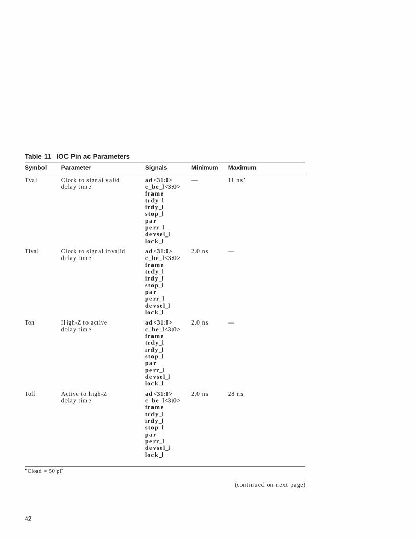
Table 11 IOC Pin ac Parameters
Symbol Parameter Signals Minimum Maximum
Tval Clock to signal validdelay time
ad<31:0>c_be_l<3:0>frametrdy_lirdy_lstop_lparperr_ldevsel_llock_l
— 11 ns�
Tival Clock to signal invaliddelay time
ad<31:0>c_be_l<3:0>frametrdy_lirdy_lstop_lparperr_ldevsel_llock_l
2.0 ns —
Ton High-Z to activedelay time
ad<31:0>c_be_l<3:0>frametrdy_lirdy_lstop_lparperr_ldevsel_llock_l
2.0 ns —
Toff Active to high-Zdelay time
ad<31:0>c_be_l<3:0>frametrdy_lirdy_lstop_lparperr_ldevsel_llock_l
2.0 ns 28 ns
�Cload = 50 pF
(continued on next page)
42

Table 11 (Cont.) IOC Pin ac Parameters
Symbol Parameter Signals Minimum Maximum
Tsu Input signal validsetup time
ad<31:0>c_be_l<3:0>frametrdy_lirdy_lstop_lparperr_ldevsel_llock_lmemreq_l
7.0 ns —
Th Input signal hold time ad<31:0>c_be_l<3:0>frametrdy_lirdy_lstop_lparperr_ldevsel_llock_lmemreq_l
0.0 ns —
Tackv Valid delay time fromclock rising edge
memack_l 3.6 ns 15 ns�
Tval-side Signal valid delay time req_l — 12 ns
Tsu-side Signal valid setup time gnt_l 12 ns —
�Cload = 50 pF
If a 5-V signaling environment is used on the PCI bus, the pll_5v pin mustbe connected to a 5-V supply. Table 12 (abridged from the PCI Local BusSpecification, Revision 2.0) specifies the ac parameters for 5-V signaling.
43

Table 12 ac Specifications for 5-V Signaling
Symbol Parameter Condition Minimum Maximum Unit
Icl Low clampcurrent
�5 < Vin � �1 �25 + (Vin + 1) / 0.015 — mA
Tr Unloadedoutputrise time
0.4 V to 2.4 V 1 — V/ns
Tf Unloadedoutputfall time
2.4 V to 0.4 V 1 — V/ns
44

Table 13 lists the JTAG pin ac parameters.
Table 13 JTAG Pin ac Parameters
Symbol Parameter Signals Minimum Maximum Unit Comments
Tjf Frequency tck 0 10 MHz —
Tjp Period tck 100 — ns —
Tjht High time tck 45 — ns —
Tjlt Low time tck 45 — ns —
Tjrt Rise time tck — 10 ns Measured between 0.8 V and2.0 V
Tjft Fall time tck — 10 ns Measured between 2.0 V and0.8 V
Tjs Setup time tditms
10 — ns With respect to tck rising edge
Tjh Hold time tditms
25 — ns With respect to tck rising edge
Tjd Valid delay tdo — 30 ns With respect to tck falling edgeCload = 50 pF
Tjfd Float delay tdo — 30 ns With respect to tck falling edge
Table 14 lists the ac parameters for the miscellaneous pins. The parametersspecified are for test purposes only and are measured with respect to thetest_clk_out signal.
Table 14 Miscellaneous Pin ac Parameters
Symbol Parameter Signals Minimum Maximum
Tmst Setup time irq<2:0>sromd
5 ns —
Tmht Hold time irq<2:0>sromd
0 ns —
45

4 Mechanical SpecificationsFigures 4 and 5 show the 287-pin standard pin grid array (PGA) package andits dimensions.
Figure 4 21066/21066A Package—Top and Side
0.050 TYP
0.195 TYP
0.018 TYP
LID
0.005 TYP R0.250
10−32 STUD
1.130 TYP
(2X)
1.130 TYP
0.850 TYP
1.250 TYP HEAT SLUG BASE AREA
CHAMFER(0.010 X 45°)
0.035 0.005 TYP±
2.260 0.014 TYP ±DIM "A"
DIM "A" =
For 21066:
For 21066A:
0.106 0.011±
0.069 0.007±
CHAMFER(0.010 X 45°)
46

Figure 5 21066/21066A Package—Bottom
1.050
ABAAYWVUTRPNMLKJHGFEDCBA
1 287X2
STANDOFF(4X)
3 0.065 TYP4
A01 POSITIONINDICATOR
5BRAZE PAD
6 7 8 9 10 11 12 13 14 15 16 1718 19 20 21 22
1.050
0.100 TYP0.100 TYP
47

5 Thermal SpecificationsSections 5.1 and 5.2 specify the 21066 operating temperature and thermalresistance.
5.1 Operating TemperatureThe operating temperature (Tc) of the 21066 is measured at the center of theheat sink between the two package studs. The 21066 is specified to operatewithin a temperature range from 0°C to Tc (maximum), which is based onthe operating frequency of the chip. Table 15 gives the maximum operatingtemperatures for the 21066.
Table 15 Maximum T c at Various Frequencies
Tc (Maximum)
Frequency 21066 21066A
100 MHz — 93°C
166 MHz 85°C —
233 MHz — 84°C
266 MHz — 70°C
5.2 Thermal ResistanceThe following equations define the heat-sink-to-ambient thermal resistancevalues:
�hs�a =(Tc�Ta)
P
Tc = Ta + P � �hs�a
The symbols in the previous equations are defined as follows:
�hs�a is the heat-sink-to-ambient thermal resistance (°C/W).Ta is the ambient temperature (°C).Tc is the case temperature measured at a predefined location on the
heat sink (°C).P is the power dissipation (W). See Section 3.3, which details chip power
consumption at various frequencies.
48

Table 16 lists the �hs�a values for several heat sinks used with the 21066287-pin ceramic PGA.
Note
The heat sink greatly improves the ambient temperature requirementand Digital recommends its use.
Table 16 �hs�a at Various Airflows
�hs�a with:
Airflow (ft/min) Heat Sink 1 Heat Sink 2 Heat Sink 3
50 2.65 3.70 7.35
100 1.95 2.80 6.55
200 1.35 1.85 5.00
400 1.00 1.30 3.10
600 0.85 1.10 2.10
800 0.7 0.9 1.65
Heat sink 1 (11 fins): 2.55 � 2.55 � 1.2 in (6.5 � 6.5 � 3.0 cm)
Heat sink 2 (13 fins): 2.27 � 2.27 � 0.9 in (5.8 � 5.8 � 2.3 cm)
Heat sink 3 (14 fins): 2.38 � 2.10 � 0.3 in (6.0 � 5.3 � 0.8 cm)
All heat sinks are unidirectional and made of aluminium alloy 6063.
The GRAFOIL pad is the interface material between the package and heat sink.
49

6 Register SummaryThe tables in this section provide a summary of the 21066 implementation-specific internal processor registers (IPRs), the memory controllerregisters, and the I/O controller (IOC) registers. For information aboutthe architecturally specified IPRs, see the Alpha Architecture ReferenceManual.
Table 17 21066-Specific Internal Processor Registers
Mnemonic Register Name Field � Index �
Instruction Fetch and Decode Unit Registers
ASTER Asynchronous system trap interrupt enable IBX 18ASTRR Asynchronous system trap request IBX 14EXC_ADDR Exception address IBX 4EXC_SUM Exception summary IBX 10HIER Hardware interrupt enable IBX 16HIRR Hardware interrupt request IBX 12ICCSR Instruction cache control and status IBX 2ITBASM Instruction translation buffer address space
matchIBX 7
ITBIS Instruction translation buffer initial state IBX 8ITB_PTE Instruction translation buffer page table entry IBX 1ITB_PTE_TEMP Instruction translation buffer page table entry
temporaryIBX 3
ITBZAP Instruction translation buffer ZAP IBX 6PAL_BASE Programmable array logic (PAL) base address IBX 11PS Processor status IBX 9SIER Software interrupt enable IBX 17SIRR Software interrupt request IBX 13SL_CLR Clear serial line interrupt IBX 19SL_RCV Serial line receive IBX 5SL_XMIT Serial line transmit IBX 22TB_TAG Translation buffer tag IBX 0
Load and Store Unit Registers
ABOX_CTL Load and store unit (Abox) control ABX 14ALT_MODE Alternate processor mode ABX 15CC Cycle counter ABX 16
�HW_MFPR and HW_MTPR instruction fields: PAL, ABX, IBX, and Index (<7,6,5,4:0>).
(continued on next page)
50

Table 17 (Cont.) 21066-Specific Internal Processor Registers
Mnemonic Register Name Field � Index �
Load and Store Unit Registers
CC_CTL Cycle counter control ABX 17DC_STAT‡ Data cache status ABX 12C_STAT† Cache status ABX 12DTBASM Data translation buffer address space match ABX 7DTB_CTL Data translation buffer control ABX 0DTBIS Data translation buffer invalidate single ABX 8DTB_PTE Data translation buffer page table entry ABX 2DTB_PTE_TEMP Data translation buffer page table entry
temporaryABX 3
DTBZAP Data translation buffer ZAP ABX 6FLUSH_IC Flush instruction cache ABX 21FLUSH_IC_ASM Flush instruction cache address space match ABX 23MM_CSR Memory management control and status ABX 4VA Virtual address ABX 5
PAL Temporary Registers
PAL_TEMP<31:0> PAL_TEMP internal processor PAL 31..0
�HW_MFPR and HW_MTPR instruction fields: PAL, ABX, IBX, and Index (<7,6,5,4:0>).†Implemented in the 21066A only.‡Implemented in the 21066 only.
Table 18 Memory Controller Registers
Mnemonic Register NameAddress(Hexadecimal)
BCR0 Bank configuration 0 1 2000 0000BCR1 Bank configuration 1 1 2000 0008BCR2 Bank configuration 2 1 2000 0010BCR3 Bank configuration 3 1 2000 0018BMR0 Bank mask 0 1 2000 0020BMR1 Bank mask 1 1 2000 0028BMR2 Bank mask 2 1 2000 0030BMR3 Bank mask 3 1 2000 0038BTR0 Bank timing 0 1 2000 0040
(continued on next page)
51

Table 18 (Cont.) Memory Controller Registers
Mnemonic Register NameAddress(Hexadecimal)
BTR1 Bank timing 1 1 2000 0048BTR2 Bank timing 2 1 2000 0050BTR3 Bank timing 3 1 2000 0058GTR Global timing 1 2000 0060ESR Error status 1 2000 0068EAR Error address 1 2000 0070CAR Cache control 1 2000 0078VGR Video and graphics control 1 2000 0080PLM Plane mask 1 2000 0088FOR Foreground 1 2000 0090PMR� Power management register 1 2000 0098
�Implemented in the 21066A only.
Table 19 I/O Controller Registers
Mnemonic Register NameAddress(Hexadecimal)
IOC_HAE Host address extension 1 8000 0000IOC_CFG Configuration cycle type 1 8000 0020IOC_STAT0 Status 0 1 8000 0040IOC_STAT1 Status 1 1 8000 0060IOC_TBIA Translation buffer invalidate all 1 8000 0080IOC_TB_ENA Translation buffer enable 1 8000 00A0IOC_SFT_RST PCI soft reset 1 8000 00C0IOC_PAR_DIS Parity disable 1 8000 00E0IOC_W_BASE0 Window base 0 1 8000 0100IOC_W_BASE1 Window base 1 1 8000 0120IOC_W_MASK0 Window mask 0 1 8000 0140IOC_W_MASK1 Window mask 1 1 8000 0160IOC_T_BASE0 Translated base 0 1 8000 0180IOC_T_BASE1 Translated base 1 1 8000 01A0IOC_TB_TAG0 Translation buffer tag 0 1 8100 0000IOC_TB_TAG1 Translation buffer tag 1 1 8100 0020IOC_TB_TAG2 Translation buffer tag 2 1 8100 0040IOC_TB_TAG3 Translation buffer tag 3 1 8100 0060IOC_TB_TAG4 Translation buffer tag 4 1 8100 0080
(continued on next page)
52

Table 19 (Cont.) I/O Controller Registers
Mnemonic Register NameAddress(Hexadecimal)
IOC_TB_TAG5 Translation buffer tag 5 1 8100 00A0IOC_TB_TAG6 Translation buffer tag 6 1 8100 00C0IOC_TB_TAG7 Translation buffer tag 7 1 8100 00E0IOC_IACK_SC Interrupt vector and special cycle �
�Any quadword-aligned address in the range 1A0000000..1BFFFFFE0.
53

7 Instruction SummaryThe tables in this section summarize the common instructions implementedby the Alpha architecture, the PALmode instructions required by all Alphaimplementations, and the architecturally reserved PALmode instructionsimplemented in the 21066 microprocessor. The instruction summaries arecontained in the following tables:
Instructions Table
Memory integer load and store 20Integer control 21Integer arithmetic 22Logical and shift 23Byte manipulation 24Memory format floating-point 25Floating-point branch 26Floating-point operate 27Miscellaneous 28VAX compatibility instructions 29Required PALmode 30Architecturally reserved PALmode 31
Table 20 Memory Integer Load and Store Instructions
Mnemonic Operation
LDA Load addressLDAH Load address high
LDL Load sign-extended longwordLDL_L Load sign-extended longword lockedLDQ Load quadwordLDQ_L Load quadword lockedLDQ_U Load quadword unaligned
STL Store longwordSTL_C Store longword conditionalSTQ Store quadwordSTQ_C Store quadword conditionalSTQ_U Store quadword unaligned
54

Table 21 Integer Control Instructions
Mnemonic Operation
BEQ Branch if register equal to zeroBGE Branch if register greater than or equal to zeroBGT Branch if register greater than zeroBLBC Branch if register low bit is clearBLBS Branch if register low bit is setBLE Branch if register less than or equal to zeroBLT Branch if register less than zeroBNE Branch if register not equal to zero
BR Unconditional branchBSR Branch to subroutine
JMP JumpJSR Jump to subroutineRET Return from subroutineJSR_COROUTINE Jump to subroutine return
Table 22 Integer Arithmetic Instructions
Mnemonic Operation
ADD Add quadword/longwordS4ADD Scaled add by 4S8ADD Scaled add by 8
CMPEQ Compare signed quadword equalCMPLT Compare signed quadword less thanCMPLE Compare signed quadword less than or equal
CMPULT Compare unsigned quadword less thanCMPULE Compare unsigned quadword less than or equal
MUL Multiply quadword/longwordUMULH Multiply quadword unsigned high
SUB Subtract quadword/longwordS4SUB Scaled subtract by 4S8SUB Scaled subtract by 8
55

Table 23 Logical and Shift Instructions
Mnemonic Operation
AND Logical productBIC Logical product with complementBIS Logical sum (OR)EQV Logical equivalence (XORNOT)ORNOT Logical sum with complementXOR Logical difference
CMOVxx Conditional move integer
SLL Shift left logicalSRA Shift right arithmeticSRL Shift right logical
Table 24 Byte-Manipulation Instructions
Mnemonic Operation
CMPBGE Compare byte
EXTBL Extract byte lowEXTWL Extract word lowEXTLL Extract longword lowEXTQL Extract quadword lowEXTWH Extract word highEXTLH Extract longword highEXTQH Extract quadword high
INSBL Insert byte lowINSWL Insert word lowINSLL Insert longword lowINSQL Insert quadword lowINSWH Insert word highINSLH Insert longword highINSQH Insert quadword high
MSKBL Mask byte lowMSKWL Mask word lowMSKLL Mask longword lowMSKQL Mask quadword low
(continued on next page)
56

Table 24 (Cont.) Byte-Manipulation Instructions
Mnemonic Operation
MSKWH Mask word highMSKLH Mask longword highMSKQH Mask quadword high
ZAP Zero bytesZAPNOT Zero bytes not
Table 25 Memory Format Floating-Point Instructions
Mnemonic Operation Subset
LDF Load F_floating VAXLDG Load G_floating (load D_floating) VAXLDS Load S_floating (load longword integer) IEEE and VAXLDT Load T_floating (load quadword integer) IEEE and VAX
STF Store F_floating VAXSTG Store G_floating (store D_floating) VAXSTS Store S_floating (store longword integer) IEEE and VAXSTT Store T_floating (store quadword integer) IEEE and VAX
Table 26 Floating-Point Branch Instructions
Mnemonic Operation Subset
FBEQ Floating branch equal IEEE and VAXFBGE Floating branch greater than or equal IEEE and VAXFBGT Floating branch greater than IEEE and VAXFBLE Floating branch less than or equal IEEE and VAXFBLT Floating branch less than IEEE and VAXFBNE Floating branch not equal IEEE and VAX
57

Table 27 Floating-Point Operate Instructions
Mnemonic Operation Subset
Arithmetic Operations
ADDF Add F_floating VAXADDG Add G_floating VAXADDS Add S_floating IEEEADDT Add T_floating IEEE
CMPGxx Compare G_floating VAXCMPTxx Compare T_floating IEEE
CVTDG Convert D_floating to G_floating VAXCVTGD Convert G_floating to D_floating VAXCVTGF Convert G_floating to F_floating VAXCVTGQ Convert G_floating to quadword VAXCVTQF Convert quadword to F_floating VAXCVTQG Convert quadword to G_floating VAXCVTQS Convert quadword to S_floating IEEECVTQT Convert quadword to T_floating IEEECVTST Convert S_floating to T_floating IEEECVTTQ Convert T_floating to quadword IEEECVTTS Convert T_floating to S_floating IEEE
DIVF Divide F_floating VAXDIVG Divide G_floating VAXDIVS Divide S_floating IEEEDIVT Divide T_floating IEEE
MULF Multiply F_floating VAXMULG Multiply G_floating VAXMULS Multiply S_floating IEEEMULT Multiply T_floating IEEE
SUBF Subtract F_floating VAXSUBG Subtract G_floating VAXSUBS Subtract S_floating IEEESUBT Subtract T_floating IEEE
(continued on next page)
58

Table 27 (Cont.) Floating-Point Operate Instructions
Mnemonic Operation Subset
Bit and FPCR Operations
CPYS Copy sign IEEE and VAXCPYSE Copy sign and exponent IEEE and VAXCPYSN Copy sign negate IEEE and VAX
CVTLQ Convert longword to quadword IEEE and VAXCVTQL Convert quadword to longword IEEE and VAX
FCMOVxx Floating conditional move IEEE and VAX
MF_FPCR Move from floating-point control register IEEE and VAXMT_FPCR Move to floating-point control register IEEE and VAX
Table 28 Miscellaneous Instructions
Mnemonic Operation
CALL_PAL Call privileged architecture library routineEXCB Exception barrierFETCH Prefetch dataFETCH_M Prefetch data, modify intentMB Memory barrierRPCC Read process cycle counterTRAPB Trap barrierWMB Write memory barrier
Table 29 VAX Compatibility Instructions
Mnemonic Operation
RC Read and clearRS Read and set
59

Table 30 Required PALmode Instructions
Mnemonic Operation
HALT Halt processorIMB Instruction stream memory barrier
Table 31 Architecturally Reserved PALmode Instructions
Mnemonic Operation
HW_MTPR Move data to processor registerHW_MFPR Move data from processor registerHW_LD Move data from memoryHW_ST Move data to memoryHW_REI Return from PALmode exception
60

Technical Support and Ordering Information
Technical SupportIf you need technical support or help deciding which literature best meets yourneeds, call the Digital Semiconductor Information Line:
United States and CanadaOutside North America
1–800–332–2717+1–508–628–4760
Ordering Digital Semiconductor ProductsTo order the Alpha 21066 or Alpha 21066A microprocessors, contact your localdistributor.
You can order the following semiconductor products from Digital:
Product Order Number
21066-166 microprocessor 21066–AA
21066A–233 microprocessor 21066–AB
21066A–100 microprocessor 21066–CB
21066A–266 microprocessor 21066–DB
Ordering Associated LiteratureThe following table lists some of the available Digital Semiconductor literature.For a complete list, contact the Digital Semiconductor Information Line.
Title Order Number
Alpha Architecture Reference Manual1 EY–L520E–DP–YCH
1To order and purchase the Alpha Architecture Reference Manual, call 1–800–DIGITAL fromthe U.S. or Canada, or contact your local Digital office, or technical or reference bookstore whereDigital Press books are distributed by Prentice Hall.

Ordering Third-Party LiteratureYou can order the following third-party literature directly from the vendor.
Title Vendor
PCI Local Bus Specification,Revision 2.0
PCI Special Interest Group1–800–433–5177 (U.S.)1–503–797–4207 (International)1–503–234–6762 (FAX)
IEEE Standard for BinaryFloating-Point Arithmetic(ANSI/IEEE Standard 754-1985)
IEEE Service Center445 Hoes LaneP.O. Box 1331Piscataway, NJ 08855-13311–800–678–IEEE (U.S. and Canada)908–562–3805 (Outside U.S. and Canada)