amba axi4 to ibm capi adapter application note … · axi4 is the de facto protocol for creating...
TRANSCRIPT
XAPP1293 (v1.0) August 8, 2016 www.xilinx.com 1
SummaryThe IBM Coherent Accelerator Processor Interface (CAPI) connects a custom acceleration engine to the coherent fabric of the POWER8 processor to deliver hybrid high-performance solutions. However, most Xilinx® IP cores use AXI4 as the standard interface, and the Vivado® Design Suite IP integrator uses an AXI4-based infrastructure to build complex IP systems. To repurpose existing Xilinx IP cores and the Vivado IP integration infrastructure, the adapter discussed in this application note is needed to convert the AXI4 interfaces to CAPI.
This application note explains the functionality, design, and implementation of the AMBA AXI4 to CAPI adapter. It also documents limitations of this adapter. An example design is provided that runs on the Alpha Data ADM-PCIE-7V3 card to illustrate the design flow when using this design to develop a hybrid system for POWER8-based systems with CAPI-attached accelerators. The ADM-PCIE-7V3 card is based on the Virtex®-7 XC7VX690T-2FFG1157C FPGA.
Part of the AMBA AXI4 to CAPI adapter and the accelerator functional unit (AFU) in the provided example design is developed with the Xilinx Vivado High-Level Synthesis (HLS) tool, which uses C language source code to generate highly efficient, synthesizable, Verilog and VHDL code.
You can download the Reference Design Files for the example design from the Xilinx website. For detailed information about the design files, see Reference Design.
Note: The reference design also includes the Memcopy accelerator function unit (AFU).
IntroductionAXI4 is the de facto protocol for creating SoCs and is used by Xilinx IP cores as the standard interface. AXI4 detailed information is available in the AMBA AXI and ACE Protocol Specification [Ref 1]. AXI4 includes three types of interfaces:
• AXI4: Used for high-performance, memory-mapped communications. AXI4 allows burst of up to 256 data transfer cycles with just a single address phase.
• AXI4-Lite: Used for simple, low-throughput, memory-mapped communications. It supports one data transfer cycle with a single address phase, unlike AXI4, which has burst support.
• AXI4-Stream: Used for high-speed streaming data applications. AXI4-Stream removes the requirement for an address phase and allows unlimited data burst size.
Application Note: Virtex-7 FPGAs
XAPP1293 (v1.0) August 8, 2016
AMBA AXI4 to IBM CAPI AdapterAuthors: Lisa Liu and Mark Paluszkiewicz
Introduction
XAPP1293 (v1.0) August 8, 2016 www.xilinx.com 2
AXI4 also uses READY/VALID handshake signals to support flow control of forward and reverse data transfer directions.
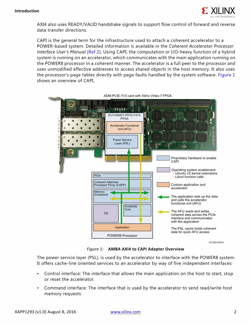
CAPI is the general term for the infrastructure used to attach a coherent accelerator to a POWER-based system. Detailed information is available in the Coherent Accelerator Processor Interface User's Manual [Ref 2]. Using CAPI, the computation or I/O-heavy function of a hybrid system is running on an accelerator, which communicates with the main application running on the POWER8 processor in a coherent manner. The accelerator is a full peer to the processor and uses unmodified effective addresses to access shared objects in the host memory. It also uses the processor's page tables directly with page faults handled by the system software. Figure 1 shows an overview of CAPI.
The power service layer (PSL), is used by the accelerator to interface with the POWER8 system. It offers cache-line oriented services to an accelerator by way of five independent interfaces:
• Control interface: The interface that allows the main application on the host to start, stop or reset the accelerator.
• Command interface: The interface that is used by the accelerator to send read/write host memory requests.
X-Ref Target - Figure 1
Figure 1: AMBA AXI4 to CAPI Adapter Overview

Implementation Details
XAPP1293 (v1.0) August 8, 2016 www.xilinx.com 3
• Response interface: The interface that is used to acknowledge the accelerator about the completed commands.
• Write buffer and read buffer interface: The interface that is used by the accelerator to send and receive data to, or from, the host memory.
• MMIO interface: The interface that is used by the main application on the host to access the registers within the accelerator.
There is a READY/VALID handshake in the PSL for flow control support. The data/responses are not always returned to the accelerator in the same order as the commands are issued.
The functions of the AMBA AXI4 to CAPI adapter include converting AXI4, AXI4-Lite and AXI4-Stream interfaces into the five PSL interfaces, breaking burst-wise data transfer into cache-line oriented data transfers used by the PSL, processing out-of-order responses in the PSL and supporting the READ/VALID flow-control processes used by AXI4.
Implementation DetailsThe AMBA AXI4 to CAPI adapter supports the three AXI interfaces using a flexible, high-performance, architecture. The design uses a hierarchical data-flow architecture that includes three modules:
• Low-level shim
• High-level shim
• AXI-Full, AXI-Lite to AXI-Stream adapter.
The AMBA AXI4 to CAPI adapter architecture is shown in Figure 2.
X-Ref Target - Figure 2
Figure 2: AMBA AXI4 to CAPI Adapter Architecture Block Diagram

Implementation Details
XAPP1293 (v1.0) August 8, 2016 www.xilinx.com 4
Low-Level ShimThe low-level shim module is developed in VHDL and used to convert the PSL accelerator interfaces to corresponding AXI4-Stream (axis) interfaces. It manages command stall recognition, clock domain crossing, decoupling read and write data streams, and low level error handling (parity error), buffer overflow error and other functions.
The low-level shim block diagram is shown in Figure 3.
The command interface block reads the AXI4-Stream commands from the high-level shim, sends the command, TAG, CSIZE, and Address to the PSL. The command interface block also reads the command credit count (credit_cnt) value from the response interface module for command stall recognition. Because the PSL cannot accept more than 64 commands without response, the stall recognition part in the command interface module stalls issuing commands to the PSL when the 64 command credit is running out. When this occurs, the command interface block generates back pressure to the high-level shim by deasserting the ready signal in the cmd AXI4-Stream interface signals.
X-Ref Target - Figure 3
Figure 3: Low-Level Shim Block Diagram

Implementation Details
XAPP1293 (v1.0) August 8, 2016 www.xilinx.com 5
The command stall recognition code is listed here:
-- command_stall_recognitioncroom_of <= ‘1’ when stall_ptr = cmd_cnt else ‘0’;stall_pntr <= credit_cnt + haX_croom;axi_ready <= ‘0’ when croom_of = ‘1’ else ‘1’;
In this code,
• cmd_cnt indicates the number of issued commands.
• credit_cnt indicates the number of commands that have been processed by the PSL.
• haX_croom indicates the number of commands that can be accepted by the PSL.
• The command issuing machine will stall when the stall_ptr, which equals to credit_cnt + haX_croom, is equal to cmd_cnt.
Figure 4 shows the command stall diagram.
The write buffer interface block receives host memory DATA with TAGS from the PSL write buffer interface, writes them into the WriteData FIFO, which then provides the AXI4-Stream output to the high-level shim. When errors occur like FIFO not ready, FIFO overflow and parity error, it also sends a critical error message to the control interface.
The read buffer interface block receives AXI4-Stream data from the high-level shim and stores them into a FIFO. The AXI4-Stream TDATA signal contains the cache-line data and its corresponding tag. The output of the FIFO is connected to the DATA and TAG buses of the PSL read buffer interface. It also detects parity errors, and sends the corresponding error code to the control interface once an error is detected.
The response interface block receives the response information from the PSL, which contains the response code, response tag, and recycled credits for issuing commands. These signals are cascaded into a single data bus and stores them in a FIFO. This FIFO is used to provide AXI4-Stream data to the high-level shim. It also transmits the command credit counter value to the command interface for command stall recognition. The FIFO not ready and parity error are monitored by this module and corresponding messages are sent to the control interface once an error is detected.
The Memory Mapped I/O (MMIO) block provides the accelerator function unit (AFU) descriptor information to the software drivers during the OS boot process. After the OS is booted up, the
X-Ref Target - Figure 4
Figure 4: Command Stall Diagram

Implementation Details
XAPP1293 (v1.0) August 8, 2016 www.xilinx.com 6
host request that signals in the PSL MMIO interface are concatenated into 96-bits to be stored into a FIFO, which will be used to provide the high-level shim AXI4-Stream signal. The AXI4-Stream style data from the high-level shim and, ultimately, from the accelerator is converted to 64-bit MMIO data signal to the PSL and the corresponding accelerator acknowledgment to the PSL is generated to the PSL when this data is received.
All of these modules use a clock-domain crossing logic to allow the rest of the adapter and the accelerator to run at a different clock rate than the PSL.
High-Level ShimThe high-level shim module is developed using HLS and is used to convert the AXI4-Stream-style PSL interface into memory-access-style AXI4-Stream interface.
The high-level shim block diagram is shown in Figure 5.
The main purpose of the high-level shim is to provide support for larger-than-cache-line size (128 bytes) data access. This includes command and data segmentation and reassembling, tag management, and reordering of out-of-order data and responses. The tag management basically involves generating and recycling tags. Once the system reset signal is deasserted, the tagGen block generates 64 tags, the maximum number of outstanding commands allowed in the PSL, and stores them in the freeTags FIFO. Afterwards, the tagCmd block pulls the freeTags FIFO and tags the to-be-issued PSL commands with the retrieved tags. At the same time, the
X-Ref Target - Figure 5
Figure 5: High-Level Shim Block Diagram
Implementation Details
XAPP1293 (v1.0) August 8, 2016 www.xilinx.com 7
received response tags will be reordered in the decodedResp block and pushed into the freeTags FIFO. The data and response reordering functionalities are implemented by the decodeResp block and the processWbuf block. The decodeResp re-orders the received responses by:
1. Marking the received response in a 64-entry table as a valid response.
2. Using the sorted command tags in the issuedCmds FIFO to retrieve the valid information.
3. Pushing the tags that index valid responses to the returnedTags FIFO to be recycled by the tagGen block, or to the validRdHostRespTags FIFO to re-order the received cache lines. The processWbuf block applies the similar approach to re-order the data.
The cmdDataBreakDown block implements the command and data segmentation function. It handles the conversion of the AXI commands to AFU-compatible commands, breaks the commands into cache-line memory read/write PSL commands (Read_cl_na or Write_na), attaches to each write command with a cache-line size data and passes the results to downstream pipeline stages. The afuMemCmdWr and afuMemCmdRd buses are 96 bits and contain 32-bit offset information and the 64-bit, byte-addressed, start address information. The afuMemDataWr bus is a 1024-bit signal, which can be used to push an entire cache-line into the pipeline in one cycle. After completing disassembly of each memory read/write command including data, the number of generated PSL commands and a flag indicating whether the command is read or write are then passed to genAfuCmdResp module via cmdBrkInfos stream.
The tagCmd block reads the segmented cache-line read/write commands and data, attaches the received free tags to these commands and data, and merges the read/write commands into one command stream taggedCmds.
The registCmds block reads the taggedCmds and taggedWrHostData streams, issues the commands to the low-level shim, pushes the issued command tags into issuedCmds stream to keep them in order, and stores the issued commands in a 64-entry local table. Each entry of the local table is a 5-element tuple <cmd, address, csize, value> in which the 1024-bit value field is only used for writing host memory commands. For reading host memory commands, the value field is empty. This local table is used for re-issuing a command when an error response arrives in the errRespTags stream. The tag of the error response will be used to index the table and retrieve the issued command and re-issue it again.
The decodeResp block contains a 64-entry local table. Each entry of the local table is a 2-element tuple <response code, valid>, and is indexed by the response/command tag. Whenever a response is received from the low-level shim, the corresponding entry in the local table will be updated with the valid field set as 1. The issued PSL command tags from issuedCmds stream will be used to retrieve the local table and check if the valid field is set. If it is set, then the tag will be recycled by the tagGen block and the response will be returned to the genAfuCmdResp block. The genAfuCmdResp block counts the number of received responses and compares the number to the number of PSL commands in the cmdBrkInfo stream. If these numbers match, then one response corresponding to the user command is generated and passed to afuMemCmdResp interface in the high-level shim. It continues as long as there are matching tags, in the case there have been several commands issued and several responses are received.
Implementation Details
XAPP1293 (v1.0) August 8, 2016 www.xilinx.com 8
The processWbuf block receives the cache-line data returned from low-level shim and stores it into its 64-entry local table, which is indexed with the response tags. When a tag arrives in the validRdHostRespTags streams, it will be read out by the processWbuf block and used in accessing the table and to retrieve the data. The retrieved data will be returned to the afuMemDataRd interface of the high-level shim. Note the tags in the validRdRespTags stream are already in order, therefore, the returned data from processWbuf block is also in order.
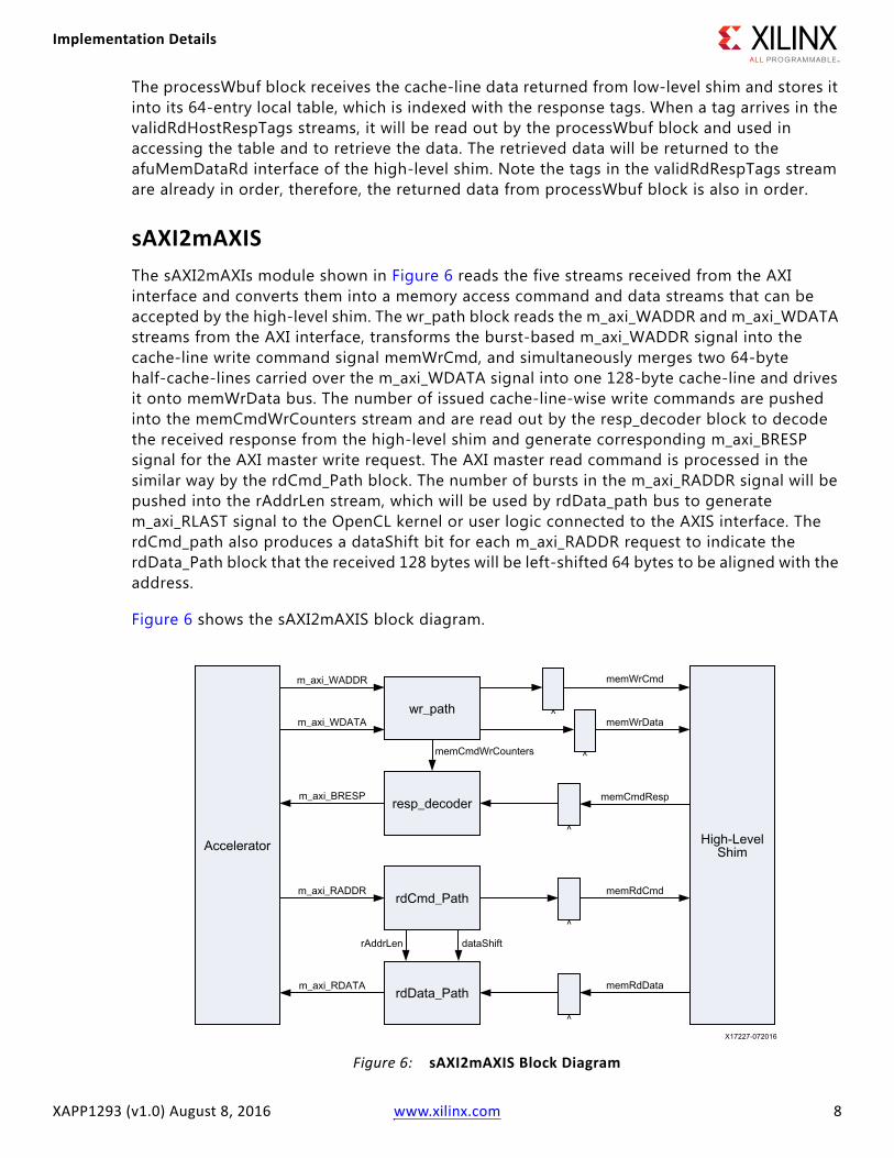
sAXI2mAXISThe sAXI2mAXIs module shown in Figure 6 reads the five streams received from the AXI interface and converts them into a memory access command and data streams that can be accepted by the high-level shim. The wr_path block reads the m_axi_WADDR and m_axi_WDATA streams from the AXI interface, transforms the burst-based m_axi_WADDR signal into the cache-line write command signal memWrCmd, and simultaneously merges two 64-byte half-cache-lines carried over the m_axi_WDATA signal into one 128-byte cache-line and drives it onto memWrData bus. The number of issued cache-line-wise write commands are pushed into the memCmdWrCounters stream and are read out by the resp_decoder block to decode the received response from the high-level shim and generate corresponding m_axi_BRESP signal for the AXI master write request. The AXI master read command is processed in the similar way by the rdCmd_Path block. The number of bursts in the m_axi_RADDR signal will be pushed into the rAddrLen stream, which will be used by rdData_path bus to generate m_axi_RLAST signal to the OpenCL kernel or user logic connected to the AXIS interface. The rdCmd_path also produces a dataShift bit for each m_axi_RADDR request to indicate the rdData_Path block that the received 128 bytes will be left-shifted 64 bytes to be aligned with the address.
Figure 6 shows the sAXI2mAXIS block diagram.
X-Ref Target - Figure 6
Figure 6: sAXI2mAXIS Block Diagram
Interface Details
XAPP1293 (v1.0) August 8, 2016 www.xilinx.com 9
mmio2axiLiteThe mmio2axiLite block converts the host mmio requests carried over the MMIO interface of high-level shim module into AXI Liter master interface, which will be used to set/get the registers in the OpenCL kernel or other user function. This module is implemented in Verilog. The conversion is a one-to-one translation. That is, the address, read/write control, and in/out data bits in the high-level shim MMIO stream interface will be directly converted into AXI lite signals. The only thing that requires special attention is that when user writes 1 to MMIO address 8 through CAPI, this write will be treated as issuing ah_jdone to the PSL control interface to inform the host software that the AFU has finished its task and ready to be unloaded. Hence, in the host side software code, after issuing MMIO write of a 1 to address 8, which will be MMIO address 2 after PSL interpretation, the host code normally calls the cxl_afu_free procedure to unload the AFU.
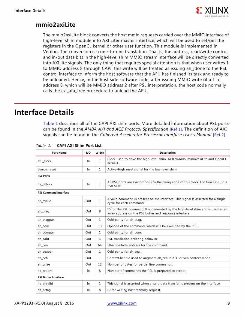
Interface DetailsTable 1 describes all of the CAPI AXI shim ports. More detailed information about PSL ports can be found in the AMBA AXI and ACE Protocol Specification [Ref 1]. The definition of AXI signals can be found in the Coherent Accelerator Processor Interface User's Manual [Ref 2].
Table 1: CAPI AXI Shim Port ListPort Name I/O Width Description
afu_clock In 1 Clock used to drive the high level-shim, sAXI2mAXIS, mmio2axiLite and OpenCL kernels.
pwron_reset In 1 Active-High reset signal for the low-level shim.
PSL Ports
ha_pclock In 1 All PSL ports are synchronous to the rising edge of this clock. For Gen3 PSL, it is 250 MHz.
PSL Command Interface
ah_cvalid Out 1 A valid command is present on the interface. This signal is asserted for a single cycle for each command.
ah_ctag Out 8 ID for the PSL command. It is generated by the high-level shim and is used as an array address on the PSL buffer and response interface.
ah_ctagpar Out 1 Odd parity for ah_ctag.
ah_com Out 13 Opcode of the command, which will be executed by the PSL.
ah_compar Out 1 Odd parity for ah_com.
ah_cabt Out 3 PSL translation ordering behavior.
ah_cea Out 64 Effective byte address for the command.
ah_ceapar Out 1 Odd parity for ah_cea.
ah_cch Out 1 Context handle used to augment ah_cea in AFU driven context mode.
ah_csize Out 12 Number of bytes for partial line commands.
ha_croom In 8 Number of commands the PSL is prepared to accept.
PSL Buffer Interface
ha_brvalid In 1 This signal is asserted when a valid data transfer is present on the interface.
ha_brtag In 8 ID for writing host memory request.
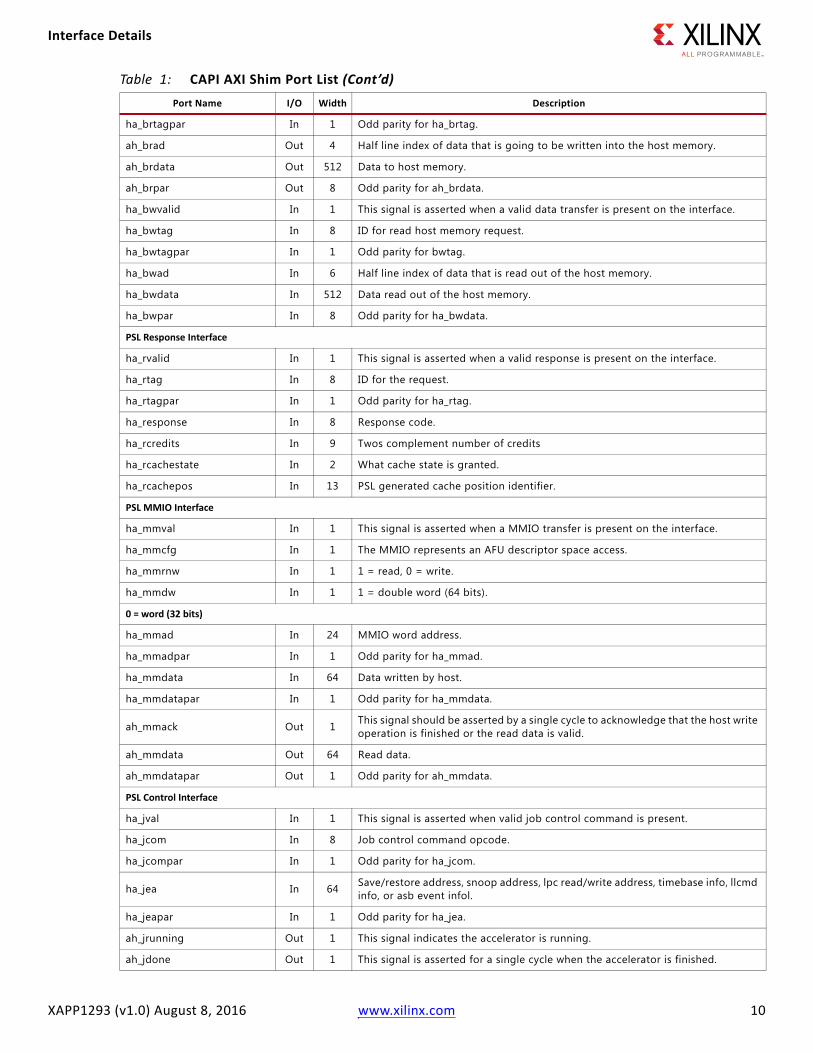
Interface Details
XAPP1293 (v1.0) August 8, 2016 www.xilinx.com 10
ha_brtagpar In 1 Odd parity for ha_brtag.
ah_brad Out 4 Half line index of data that is going to be written into the host memory.
ah_brdata Out 512 Data to host memory.
ah_brpar Out 8 Odd parity for ah_brdata.
ha_bwvalid In 1 This signal is asserted when a valid data transfer is present on the interface.
ha_bwtag In 8 ID for read host memory request.
ha_bwtagpar In 1 Odd parity for bwtag.
ha_bwad In 6 Half line index of data that is read out of the host memory.
ha_bwdata In 512 Data read out of the host memory.
ha_bwpar In 8 Odd parity for ha_bwdata.
PSL Response Interface
ha_rvalid In 1 This signal is asserted when a valid response is present on the interface.
ha_rtag In 8 ID for the request.
ha_rtagpar In 1 Odd parity for ha_rtag.
ha_response In 8 Response code.
ha_rcredits In 9 Twos complement number of credits
ha_rcachestate In 2 What cache state is granted.
ha_rcachepos In 13 PSL generated cache position identifier.
PSL MMIO Interface
ha_mmval In 1 This signal is asserted when a MMIO transfer is present on the interface.
ha_mmcfg In 1 The MMIO represents an AFU descriptor space access.
ha_mmrnw In 1 1 = read, 0 = write.
ha_mmdw In 1 1 = double word (64 bits).
0 = word (32 bits)
ha_mmad In 24 MMIO word address.
ha_mmadpar In 1 Odd parity for ha_mmad.
ha_mmdata In 64 Data written by host.
ha_mmdatapar In 1 Odd parity for ha_mmdata.
ah_mmack Out 1 This signal should be asserted by a single cycle to acknowledge that the host write operation is finished or the read data is valid.
ah_mmdata Out 64 Read data.
ah_mmdatapar Out 1 Odd parity for ah_mmdata.
PSL Control Interface
ha_jval In 1 This signal is asserted when valid job control command is present.
ha_jcom In 8 Job control command opcode.
ha_jcompar In 1 Odd parity for ha_jcom.
ha_jea In 64 Save/restore address, snoop address, lpc read/write address, timebase info, llcmd info, or asb event infol.
ha_jeapar In 1 Odd parity for ha_jea.
ah_jrunning Out 1 This signal indicates the accelerator is running.
ah_jdone Out 1 This signal is asserted for a single cycle when the accelerator is finished.
Table 1: CAPI AXI Shim Port List (Cont’d)Port Name I/O Width Description
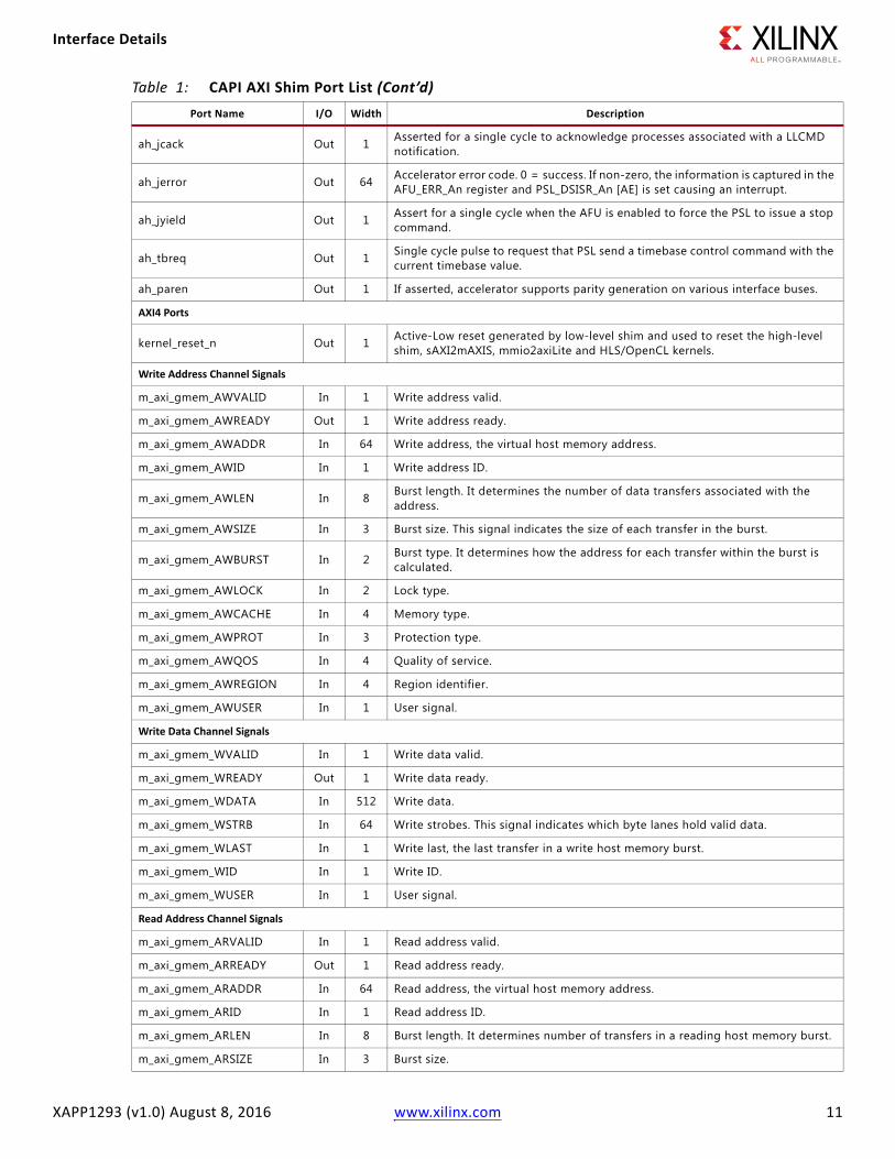
Interface Details
XAPP1293 (v1.0) August 8, 2016 www.xilinx.com 11
ah_jcack Out 1 Asserted for a single cycle to acknowledge processes associated with a LLCMD notification.
ah_jerror Out 64 Accelerator error code. 0 = success. If non-zero, the information is captured in the AFU_ERR_An register and PSL_DSISR_An [AE] is set causing an interrupt.
ah_jyield Out 1 Assert for a single cycle when the AFU is enabled to force the PSL to issue a stop command.
ah_tbreq Out 1 Single cycle pulse to request that PSL send a timebase control command with the current timebase value.
ah_paren Out 1 If asserted, accelerator supports parity generation on various interface buses.
AXI4 Ports
kernel_reset_n Out 1 Active-Low reset generated by low-level shim and used to reset the high-level shim, sAXI2mAXIS, mmio2axiLite and HLS/OpenCL kernels.
Write Address Channel Signals
m_axi_gmem_AWVALID In 1 Write address valid.
m_axi_gmem_AWREADY Out 1 Write address ready.
m_axi_gmem_AWADDR In 64 Write address, the virtual host memory address.
m_axi_gmem_AWID In 1 Write address ID.
m_axi_gmem_AWLEN In 8 Burst length. It determines the number of data transfers associated with the address.
m_axi_gmem_AWSIZE In 3 Burst size. This signal indicates the size of each transfer in the burst.
m_axi_gmem_AWBURST In 2 Burst type. It determines how the address for each transfer within the burst is calculated.
m_axi_gmem_AWLOCK In 2 Lock type.
m_axi_gmem_AWCACHE In 4 Memory type.
m_axi_gmem_AWPROT In 3 Protection type.
m_axi_gmem_AWQOS In 4 Quality of service.
m_axi_gmem_AWREGION In 4 Region identifier.
m_axi_gmem_AWUSER In 1 User signal.
Write Data Channel Signals
m_axi_gmem_WVALID In 1 Write data valid.
m_axi_gmem_WREADY Out 1 Write data ready.
m_axi_gmem_WDATA In 512 Write data.
m_axi_gmem_WSTRB In 64 Write strobes. This signal indicates which byte lanes hold valid data.
m_axi_gmem_WLAST In 1 Write last, the last transfer in a write host memory burst.
m_axi_gmem_WID In 1 Write ID.
m_axi_gmem_WUSER In 1 User signal.
Read Address Channel Signals
m_axi_gmem_ARVALID In 1 Read address valid.
m_axi_gmem_ARREADY Out 1 Read address ready.
m_axi_gmem_ARADDR In 64 Read address, the virtual host memory address.
m_axi_gmem_ARID In 1 Read address ID.
m_axi_gmem_ARLEN In 8 Burst length. It determines number of transfers in a reading host memory burst.
m_axi_gmem_ARSIZE In 3 Burst size.
Table 1: CAPI AXI Shim Port List (Cont’d)Port Name I/O Width Description
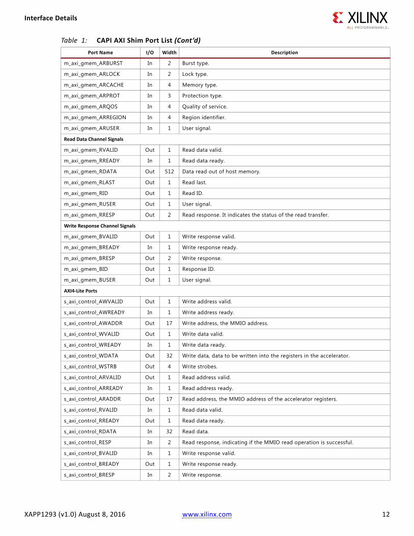
Interface Details
XAPP1293 (v1.0) August 8, 2016 www.xilinx.com 12
m_axi_gmem_ARBURST In 2 Burst type.
m_axi_gmem_ARLOCK In 2 Lock type.
m_axi_gmem_ARCACHE In 4 Memory type.
m_axi_gmem_ARPROT In 3 Protection type.
m_axi_gmem_ARQOS In 4 Quality of service.
m_axi_gmem_ARREGION In 4 Region identifier.
m_axi_gmem_ARUSER In 1 User signal.
Read Data Channel Signals
m_axi_gmem_RVALID Out 1 Read data valid.
m_axi_gmem_RREADY In 1 Read data ready.
m_axi_gmem_RDATA Out 512 Data read out of host memory.
m_axi_gmem_RLAST Out 1 Read last.
m_axi_gmem_RID Out 1 Read ID.
m_axi_gmem_RUSER Out 1 User signal.
m_axi_gmem_RRESP Out 2 Read response. It indicates the status of the read transfer.
Write Response Channel Signals
m_axi_gmem_BVALID Out 1 Write response valid.
m_axi_gmem_BREADY In 1 Write response ready.
m_axi_gmem_BRESP Out 2 Write response.
m_axi_gmem_BID Out 1 Response ID.
m_axi_gmem_BUSER Out 1 User signal.
AXI4-Lite Ports
s_axi_control_AWVALID Out 1 Write address valid.
s_axi_control_AWREADY In 1 Write address ready.
s_axi_control_AWADDR Out 17 Write address, the MMIO address.
s_axi_control_WVALID Out 1 Write data valid.
s_axi_control_WREADY In 1 Write data ready.
s_axi_control_WDATA Out 32 Write data, data to be written into the registers in the accelerator.
s_axi_control_WSTRB Out 4 Write strobes.
s_axi_control_ARVALID Out 1 Read address valid.
s_axi_control_ARREADY In 1 Read address ready.
s_axi_control_ARADDR Out 17 Read address, the MMIO address of the accelerator registers.
s_axi_control_RVALID In 1 Read data valid.
s_axi_control_RREADY Out 1 Read data ready.
s_axi_control_RDATA In 32 Read data.
s_axi_control_RESP In 2 Read response, indicating if the MMIO read operation is successful.
s_axi_control_BVALID In 1 Write response valid.
s_axi_control_BREADY Out 1 Write response ready.
s_axi_control_BRESP In 2 Write response.
Table 1: CAPI AXI Shim Port List (Cont’d)Port Name I/O Width Description
Reference Design
XAPP1293 (v1.0) August 8, 2016 www.xilinx.com 13
Reference DesignNote: The reference design also includes the Memcopy AFU.
The reference design contains all modules listed in Figure 2, where the IBM PSL is a routed netlist file called b_routed_design_adv7gen3.dcp, the accelerator is an accelerator function unit (AFU) that copies 1,024 bytes of data from one part of host memory to another. The host code in this reference design is responsible for allocating source and destination host memory, initiating the content of the source memory, and verifying the results in the destination memory.
The AFU is implemented in C programming language and compiled by the Vivado HLS tool to generate a Verilog/VHDL module that has an AXI-Full interface for data transfer and AXI-Lite interface for reading/writing control registers. The listing shown here lists the C code of the AFU:
#include <string.h>#include "ap_int.h"void opencldesign_wrapper(ap_uint<512> *a, ap_uint<512> *output){#pragma HLS INTERFACE m_axi port=a offset=slave bundle=gmem#pragma HLS INTERFACE m_axi port=output offset=slave bundle=gmem#pragma HLS INTERFACE s_axilite port=a bundle=control#pragma HLS INTERFACE s_axilite port=output bundle=control#pragma HLS INTERFACE s_axilite port=return bundle=control
ap_uint<512> bufa[16];
memcpy(bufa, (ap_uint<512> *) a, 16*64); memcpy((ap_uint<512> *) output, bufa, 16*64); return;}
You can download the Reference Design for this application note from the Xilinx website.
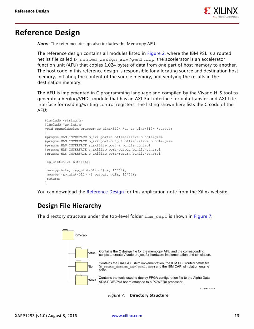
Design File HierarchyThe directory structure under the top-level folder ibm_capi is shown in Figure 7:
X-Ref Target - Figure 7
Figure 7: Directory Structure
b_route_design_adv7gen3.dcp
Running the Example Design
XAPP1293 (v1.0) August 8, 2016 www.xilinx.com 14
Running the Example Design
Required Hardware and Software• Alpha Data ADM-PCIE-7V3 high-performance reconfigurable computing card [Ref 3]. This
card is based on the Virtex-7 XC7VX690T-2FFG1157C FPGA.
• IBM Power Systems POWER8 server
° System configuration: Model 8247-21L
° Operating system: Ubuntu 15.04
• X86-based computer with Windows 7 or Linux Red Hat 5.1. The X86-based computer is used to run Vivado Design Suite and Vivado HLS tools to build the FPGA configuration file. The Windows or Linux OS versions can be higher.
• Xilinx Platform Cable USB II, part number HW-USB-II-G. Required for connecting the X86 computer to the ADM-PCIE-7V3 card and programming the FPGA (see Platform Cable USB II Data Sheet (DS593) [Ref 4].
Required Softwarethe X86 computer requires the software listed here:
• Vivado Design Suite 2015.4
• Reference Design

Running the Example Design
XAPP1293 (v1.0) August 8, 2016 www.xilinx.com 15
Install the ADM-PCIE-7V3 CardIMPORTANT: Follow manufacturer recommendations to ensure proper mounting, power requirements, and adequate cooling of the ADM-PCIE-7V3 card. See the Alpha Data ADM-PCIE-7V3 User Manual [Ref 3].
1. Locate DIP switch SW1 on the back side of the ADM-PCIE-7V3 card and set it as shown in Figure 8:
2. Install the ADM-PCIE-7V3 card into slot P1-C7 on the 8247-21L POWER8 server.
Note: Slot P1-C7 and P1-C6 are CAPI-enabled.
Set Up the X86 Computer1. If not already on the computer:
a. Install Linux.
b. Install Vivado Design Suite version 2015.4 (includes the Vivado HLS tools) on the host computer.
IMPORTANT: Include the folder that contains vivado and vivado_hls commands in the PATH environment variable setup.
Build the Design1. Unzip the Reference Design Files into a clean directory on the X86 computer and on the
POWER8 server.
2. On the X86 computer, from the installation directory, navigate to directory:ibm_capi/afus/memcpy_sdaccel/scripts.
X-Ref Target - Figure 8
Figure 8: SW1 Settings, ADM-PCIE-7V3 card

Running the Example Design
XAPP1293 (v1.0) August 8, 2016 www.xilinx.com 16
3. On the command line enter: source ./make_hw.sh.
source ./make_hw.sh will run Vivado Design Suite, open the project that contains the CAPI AXI shim and the memcpy AFU, and start synthesizing the IP cores.
4. After the IP cores are synthesized, enter source ../scripts/synImpDesign.tcl from the Tcl console as shown in the Figure 9.
5. Exit Vivado Design Suite. When asked to save the project, select Don't Save as shown in Figure 10.
6. Navigate to ibm_capi/afus/memcpy_sdaccel/scripts.
7. Enter vivado -mode batch -source write_bitstream.tcl to generate the configuration file psl_fpga_flash.bin located in directory ibm_capi/afus/memcpy_sdaccel.
X-Ref Target - Figure 9
Figure 9: TCL Console
X-Ref Target - Figure 10
Figure 10: Don’t Save Project
Running the Example Design
XAPP1293 (v1.0) August 8, 2016 www.xilinx.com 17
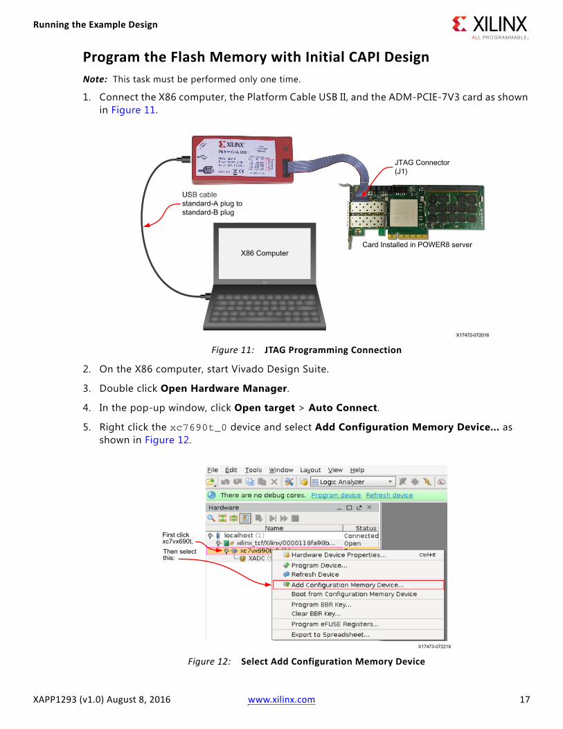
Program the Flash Memory with Initial CAPI DesignNote: This task must be performed only one time.
1. Connect the X86 computer, the Platform Cable USB II, and the ADM-PCIE-7V3 card as shown in Figure 11.
2. On the X86 computer, start Vivado Design Suite.
3. Double click Open Hardware Manager.
4. In the pop-up window, click Open target > Auto Connect.
5. Right click the xc7690t_0 device and select Add Configuration Memory Device... as shown in Figure 12.
X-Ref Target - Figure 11
Figure 11: JTAG Programming Connection
X-Ref Target - Figure 12
Figure 12: Select Add Configuration Memory Device
Wally

Running the Example Design
XAPP1293 (v1.0) August 8, 2016 www.xilinx.com 18
6. In the Add Configuration Memory Device window, search device alias name 28F00AG18F as shown in Figure 13. Click OK.
7. In the Program Configuration Memory Device window, enter ibm_capi/tools/psl_fpga.mcs in the Configuration file field (Figure 14). Click OK to start the configuration process.
8. After the configuration process finishes, power cycle (power off and then power on) the POWER8 server to enable the ADM-PCIE-7V3 card to receive the .bin file.
X-Ref Target - Figure 13
Figure 13: Choose Configuration Memory
X-Ref Target - Figure 14
Figure 14: Enter the Configuration File
Conclusion
XAPP1293 (v1.0) August 8, 2016 www.xilinx.com 19
Run the AXI4 to CAPI Adapter1. Log in to the POWER8 server as root.
IMPORTANT: Verify the LD_LIBRARY_PATH environment variable includes the ibm_capi/lib/libcxl-master path.
2. From the x86 computer, copy the configuration file psl_fpga_flash.bin to the POWER8 server in directory ibm_capi/tools.
3. On the POWER8 server, run ./capi_flash_xilinx_ad.sh psl_fpga_flash.bin.
This will first transfer the FPGA configuration file (also called the bitfile) in the psl_fpga_flash.bin to the ADM-PCIE-7V3 card flash memory, and then reset the FPGA. After the FPGA card is reset, the new FPGA configuration file that is in the flash memory is loaded into the FPGA configuration memory, and the FPGA starts to behave according to its configuration memory.
4. Navigate to the ibm_capi/lib/libcxl-master directory.
5. Enter make. The make command builds the library used by the x86 application on the POWER8 server.
6. Navigate to ibm_capi/afus/memcpy_sdaccel/sw/native.
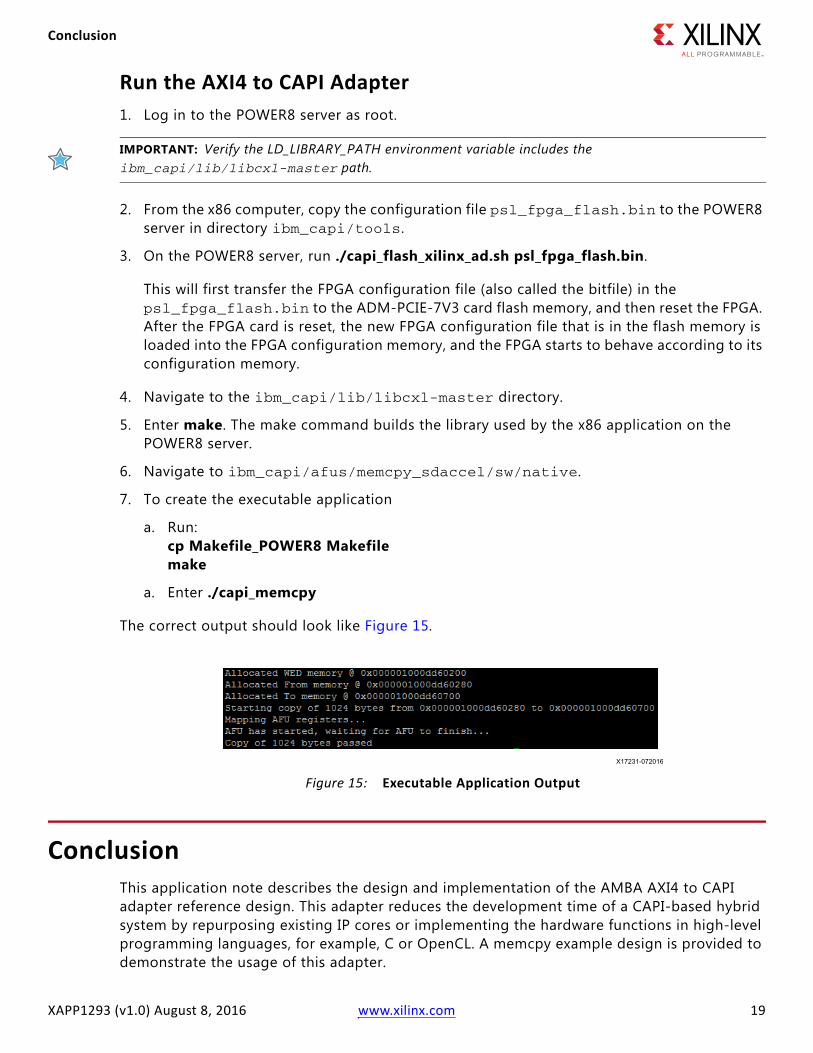
7. To create the executable application
a. Run: cp Makefile_POWER8 Makefilemake
a. Enter ./capi_memcpy
The correct output should look like Figure 15.
ConclusionThis application note describes the design and implementation of the AMBA AXI4 to CAPI adapter reference design. This adapter reduces the development time of a CAPI-based hybrid system by repurposing existing IP cores or implementing the hardware functions in high-level programming languages, for example, C or OpenCL. A memcpy example design is provided to demonstrate the usage of this adapter.
X-Ref Target - Figure 15
Figure 15: Executable Application Output
Reference Design
XAPP1293 (v1.0) August 8, 2016 www.xilinx.com 20
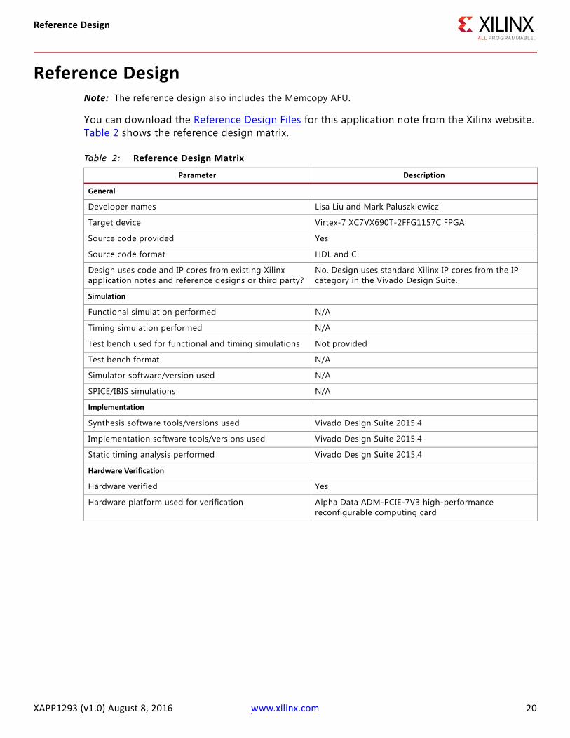
Reference DesignNote: The reference design also includes the Memcopy AFU.
You can download the Reference Design Files for this application note from the Xilinx website. Table 2 shows the reference design matrix.
Table 2: Reference Design Matrix
Parameter Description
General
Developer names Lisa Liu and Mark Paluszkiewicz
Target device Virtex-7 XC7VX690T-2FFG1157C FPGA
Source code provided Yes
Source code format HDL and C
Design uses code and IP cores from existing Xilinx application notes and reference designs or third party?
No. Design uses standard Xilinx IP cores from the IP category in the Vivado Design Suite.
Simulation
Functional simulation performed N/A
Timing simulation performed N/A
Test bench used for functional and timing simulations Not provided
Test bench format N/A
Simulator software/version used N/A
SPICE/IBIS simulations N/A
Implementation
Synthesis software tools/versions used Vivado Design Suite 2015.4
Implementation software tools/versions used Vivado Design Suite 2015.4
Static timing analysis performed Vivado Design Suite 2015.4
Hardware Verification
Hardware verified Yes
Hardware platform used for verification Alpha Data ADM-PCIE-7V3 high-performance reconfigurable computing card
References
XAPP1293 (v1.0) August 8, 2016 www.xilinx.com 21
References1. AMBA AXI and ACE Protocol Specification
https://developer.arm.com/products/architecture/amba-protocol/amba-4
2. Coherent Accelerator Processor Interface User’s Manual Xilinx Editionhttp://www.alpha-data.com/pdfs/capi-ref-design-user-guide.pdf
3. Alpha Data ADM-PCIE-7V3 high-performance reconfigurable computing cardhttp://www.alpha-data.com/dcp/products.php?product=adm-pcie-7v3
4. Platform Cable USB II Data Sheet (DS593)
Revision HistoryThe following table shows the revision history for this document.
Please Read: Important Legal NoticesThe information disclosed to you hereunder (the “Materials”) is provided solely for the selection and use of Xilinx products. To the maximum extent permitted by applicable law: (1) Materials are made available “AS IS” and with all faults, Xilinx hereby DISCLAIMS ALL WARRANTIES AND CONDITIONS, EXPRESS, IMPLIED, OR STATUTORY, INCLUDING BUT NOT LIMITED TO WARRANTIES OF MERCHANTABILITY, NON-INFRINGEMENT, OR FITNESS FOR ANY PARTICULAR PURPOSE; and (2) Xilinx shall not be liable (whether in contract or tort, including negligence, or under any other theory of liability) for any loss or damage of any kind or nature related to, arising under, or in connection with, the Materials (including your use of the Materials), including for any direct, indirect, special, incidental, or consequential loss or damage (including loss of data, profits, goodwill, or any type of loss or damage suffered as a result of any action brought by a third party) even if such damage or loss was reasonably foreseeable or Xilinx had been advised of the possibility of the same. Xilinx assumes no obligation to correct any errors contained in the Materials or to notify you of updates to the Materials or to product specifications. You may not reproduce, modify, distribute, or publicly display the Materials without prior written consent. Certain products are subject to the terms and conditions of Xilinx’s limited warranty, please refer to Xilinx’s Terms of Sale which can be viewed at http://www.xilinx.com/legal.htm#tos; IP cores may be subject to warranty and support terms contained in a license issued to you by Xilinx. Xilinx products are not designed or intended to be fail-safe or for use in any application requiring fail-safe performance; you assume sole risk and liability for use of Xilinx products in such critical applications, please refer to Xilinx’s Terms of Sale which can be viewed at http://www.xilinx.com/legal.htm#tos.Automotive Applications DisclaimerAUTOMOTIVE PRODUCTS (IDENTIFIED AS “XA” IN THE PART NUMBER) ARE NOT WARRANTED FOR USE IN THE DEPLOYMENT OF AIRBAGS OR FOR USE IN APPLICATIONS THAT AFFECT CONTROL OF A VEHICLE (“SAFETY APPLICATION”) UNLESS THERE IS A SAFETY CONCEPT OR REDUNDANCY FEATURE CONSISTENT WITH THE ISO 26262 AUTOMOTIVE SAFETY STANDARD (“SAFETY DESIGN”). CUSTOMER SHALL, PRIOR TO USING OR DISTRIBUTING ANY SYSTEMS THAT INCORPORATE PRODUCTS, THOROUGHLY TEST SUCH SYSTEMS FOR SAFETY PURPOSES. USE OF PRODUCTS IN A SAFETY APPLICATION WITHOUT A SAFETY DESIGN IS FULLY AT THE RISK OF CUSTOMER, SUBJECT ONLY TO APPLICABLE LAWS AND REGULATIONS GOVERNING LIMITATIONS ON PRODUCT LIABILITY.© Copyright 2016 Xilinx, Inc. Xilinx, the Xilinx logo, Artix, ISE, Kintex, Spartan, Virtex, Vivado, Zynq, and other designated brands included herein are trademarks of Xilinx in the United States and other countries. AMBA, AMBA Designer, ARM, ARM1176JZ-S, CoreSight, Cortex, and PrimeCell are trademarks of ARM in the EU and other countries. All other trademarks are the property of their respective owners.
Date Version Revision
08/08/2016 1.0 Initial Xilinx release.