amorphous in–ga–zn–o thin-film transistor active pixel sensor...
TRANSCRIPT

Amorphous In–Ga–Zn–O thin-film transistor active pixel sensor x-rayimager for digital breast tomosynthesis
Chumin Zhao and Jerzy Kanickia)
Solid-State Electronic Laboratory, Department of Electrical Engineering and Computer Science,University of Michigan, Ann Arbor, Michigan 48109
(Received 27 November 2013; revised 21 May 2014; accepted for publication 23 July 2014;published 12 August 2014)
Purpose: The breast cancer detection rate for digital breast tomosynthesis (DBT) is limited by the x-ray image quality. The limiting Nyquist frequency for current DBT systems is around 5 lp/mm, whilethe fine image details contained in the high spatial frequency region (>5 lp/mm) are lost. Also todaythe tomosynthesis patient dose is high (0.67–3.52 mGy). To address current issues, in this paper, forthe first time, a high-resolution low-dose organic photodetector/amorphous In–Ga–Zn–O thin-filmtransistor (a-IGZO TFT) active pixel sensor (APS) x-ray imager is proposed for next generation DBTsystems.Methods: The indirect x-ray detector is based on a combination of a novel low-cost organic photo-diode (OPD) and a cesium iodide-based (CsI:Tl) scintillator. The proposed APS x-ray imager over-comes the difficulty of weak signal detection, when small pixel size and low exposure conditions areused, by an on-pixel signal amplification with a significant charge gain. The electrical performanceof a-IGZO TFT APS pixel circuit is investigated by SPICE simulation using modified RensselaerPolytechnic Institute amorphous silicon (a-Si:H) TFT model. Finally, the noise, detective quantumefficiency (DQE), and resolvability of the complete system are modeled using the cascaded systemformalism.Results: The result demonstrates that a large charge gain of 31–122 is achieved for the proposedhigh-mobility (5–20 cm2/V s) amorphous metal-oxide TFT APS. The charge gain is sufficient toeliminate the TFT thermal noise, flicker noise as well as the external readout circuit noise. Moreover,the low TFT (<10−13 A) and OPD (<10−8 A/cm2) leakage currents can further reduce the APSnoise. Cascaded system analysis shows that the proposed APS imager with a 75 μm pixel pitch caneffectively resolve the Nyquist frequency of 6.67 lp/mm, which can be further improved to ∼10 lp/mmif the pixel pitch is reduced to 50 μm. Moreover, the detector entrance exposure per projection canbe reduced from 1 to 0.3 mR without a significant reduction of DQE. The signal-to-noise ratio ofthe a-IGZO APS imager under 0.3 mR x-ray exposure is comparable to that of a-Si:H passive pixelsensor imager under 1 mR, indicating good image quality under low dose. A threefold reduction ofcurrent tomosynthesis dose is expected if proposed technology is combined with an advanced DBTimage reconstruction method.Conclusions: The proposed a-IGZO APS x-ray imager with a pixel pitch <75 μm is capableto achieve a high spatial frequency (>6.67 lp/mm) and a low dose (<0.4 mGy) innext generation DBT systems. © 2014 American Association of Physicists in Medicine.[http://dx.doi.org/10.1118/1.4892382]
Key words: digital breast tomosynthesis, amorphous In–Ga–Zn–O thin-film transistor, active pixelsensor, cascaded system analysis, detective quantum efficiency
1. INTRODUCTION
Standard two-dimensional (2D) mammography x-ray breastimaging technology suffers a limited detection rate due tosevere breast tissue overlap.1 Digital breast tomosynthesis(DBT), as an alternative to mammography, eliminates thebreast tissue superposition issue of mammography by re-constructing a series of tomographic cross-section images.2–4
Current DBT systems consist of a moveable x-ray source, aphotodetector, and an active-matrix thin-film transistor (TFT)array.5–7 The x-ray source motion for tomosynthesis can beeither “step and shoot” or “continuous.”8 The step and shootmotion reduces image blur due to x-ray source motion, whileincreases image blur due to human motion with increased to-tal scan time.8, 9 During the acquisition time (3.7–25 s), 9–25
low-dose projection images are obtained from a total scan an-gle from 15◦ to 45◦.9, 10 Increasing the total scan angle pro-vides better vertical resolution. However, large number ofprojection images will prolong the total scan time and willincrease the total dose.9 Optimizing the image acquisition pa-rameters for low dose is still under research.8, 11, 12
The technical specifications of several clinically approvedDBT systems (GE Essential, Hologic Selenia Dimensions,and Siemens Mammomat Inspiration) and the proposed nextgeneration tomosynthesis system are shown in Table I.5–7, 9, 10
Clinically, the obtained image quality needs to be op-timized for radiologists to distinguish microcalcificationdetails.13 The limiting spatial frequency (Nyquist frequency)is defined as 1/(2apix), where apix is the pixel pitch. A pixelpitch of ∼100 μm corresponds to the Nyquist frequency
091902-1 Med. Phys. 41 (9), September 2014 © 2014 Am. Assoc. Phys. Med. 091902-10094-2405/2014/41(9)/091902/14/$30.00

091902-2 C. Zhao and J. Kanicki: Amorphous IGZO TFT APS x-ray imager for DBT 091902-2
TABLE I. Technical specifications of digital breast tomosynthesis imaging systems.
Hologic Selenia Siemens MammomatGE Essentiala Dimensions Inspiration Proposed system
Detector CsI:Tl/a-Si:H p-i-n a-Se (direct) a-Se (direct) CsI:Tl/organic photodiode(indirect) (indirect)
TFT technology a-Si:H TFT a-Si:H TFT a-Si:H TFT a-InGaZnO TFTDetector size (cm) 24 × 30 24 × 29 24 × 30 24 × 30Pixel resolution 2394 × 3062 1664 × 2048 (2 × 2 binning) 2816 × 3584 3200 × 4000Pixel layout Side by side Side by side Side by side Vertically stackedPixel pitch (μm) 100 140 (2 × 2 binning) 85 <75Pixel fill factor 0.5–0.8 0.5–0.8 0.5–0.8 >0.8Limiting spatial resolution (lp/mm) ∼5 ∼5 ∼6 >6.67Pixel circuit Passive pixel sensor Passive pixel sensor Passive pixel sensor Active pixel sensorScan time (s) 7 3.7 25 < 4Total scan angle 25◦ 15◦ 45◦ NAX-ray source motion Step and shoot Continuous Continuous ContinuousDetector motion Static Rotating Static RotatingNumber of views 9 15 25 NAMean glandular dose (mGy) NA 0.67–2.64b NA <0.4c
aThe next generation imager is GE SenoClaire. No technical details are available.bThe MGD is for breasts of 2–8 cm thickness and 50% glandular fraction. The dose is 1.3 mGy for an average breast (50% glandular fraction, 5 cm thick) and can be ashigh as 3.52 mGy for dense breasts.
cCascaded system analysis shows that the detector x-ray exposure can be reduced by threefold without influencing the image quality significantly using the APS imager.Therefore, a 3× dose reduction is expected in combination with an advanced image reconstruction method.
(fNyquist) of 5 lp/mm due to the aliasing.14 Higher spatialfrequency (>5 lp/mm) can provide fine image details thatshould not be lost. A pixel pitch of <75 μm is requiredto resolve spatial frequency of >6.67 lp/mm. As shown inTable I, DBT systems with pixel pitch around 100 μm havebeen developed based on amorphous silicon (a-Si:H) TFTpassive pixel sensor (PPS).9, 10, 15, 16 Hologic Selenia Dimen-sions detector has a pixel pitch of 70 μm for mammography,but a 2 × 2 binning technology is generally used for DBT re-sulting in an effective pixel pitch of 140 μm.10 In PPS, it isdifficult to further reduce the pixel size due to the weak sig-nal caused by the low detector entrance exposure per projec-tion (∼1 mR) (Ref. 7) during tomosynthesis. We use the unitRoentgen (R) to define the x-ray exposure to the detector andGray (Gy) to measure the patient glandular dose; 1 R is equalto 8.76 mGy of absorbed dose in dry air. For small pixel sizeand under low x-ray exposure conditions, the electronic noisebecomes significant and will result in a limited signal-to-noiseratio (SNR) and a low detective quantum efficiency (DQE).17
In addition, the detectable input signal is further attenuated bythe pixel fill factor (FF) (0.4–0.8),15, 18 which is defined by theratio of photodiode active area over the entire pixel area. As aresult, the detector entrance exposure per projection (∼1 mR)and patient mean glandular dose (MGD) remain high to com-pensate for weak signal. Feng et al. reported that the MGDfor breasts of 2–8 cm thickness and 50% glandular fractionis 0.67–2.64 mGy (1.3 mGy for a 5 cm thick average breast)and can be as high as 3.52 mGy for dense breasts.6 The doseof a single-view DBT exam is about one to two times thatof a single-view full-field digital mammogram (FFDM).19
The question of dose optimization for DBT has not beensolved yet.
To achieve a high spatial frequency (>6.67 lp/mm) anda low patient dose (<0.4 mGy), we propose a verticallyintegrated indirect organic photodetector/amorphous In–Ga–Zn–O (a-IGZO) TFT active pixel sensor (APS) x-ray im-ager for next generation low dose DBT systems. In contrastto PPS, APS amplifies the input signal on the pixel leveland minimizes the influence of electronic noise by a chargegain.20–22, 25 The a-IGZO TFT array is vertically stacked incombination with a low-cost poly(3-hexylthiophene):phenyl-C61-butyric acid methyl ester (P3HT:PCBM) organic pho-todiode (OPD) (Refs. 23–26) and a thallium-doped cesiumiodide (CsI:Tl) scintillator,27, 28 which addresses the dimin-ishing FF issue when small pixel size is used. The electri-cal performance of the proposed a-IGZO TFT APS is studiedby SPICE circuit simulation using the Rensselaer Polytech-nic Institute (RPI) a-Si:H TFT model modified for a-IGZOTFT.29 The noise and DQE of the active pixel a-IGZO TFT-based high-resolution x-ray imager are investigated using thecascaded system model in Sec. 4.18, 30–32
2. X-RAY DETECTOR
2.A. Direct conversion detector
In general, DBT systems can be categorized into di-rect (Hologic Selenia Dimensions, and Siemens Mam-momat Inspiration) and indirect conversion detectors (GEEssential).9, 10 For direct conversion detectors, as shown inFig. 1(a), x-ray photons are absorbed by semiconductorssuch as amorphous selenium (a-Se) photodiodes and di-rectly converted to electric signal.33, 34 Compared to indirectdetectors, direct conversion detectors eliminate problems as-sociated with the light scattering of the scintillator, which can
Medical Physics, Vol. 41, No. 9, September 2014

091902-3 C. Zhao and J. Kanicki: Amorphous IGZO TFT APS x-ray imager for DBT 091902-3
FIG. 1. Schematics of (a) direct and (b) indirect conversion detectors areshown. An a-Se photodiode and a conventional a-Si:H p-i-n photodiode areused for indirect and direct conversion detectors, respectively.
be an issue for high resolution DBT.33 The incident noisepower spectrum (NPS) for direct conversion detectors extendwell above the fNyquist. The aliasing and back-folding of NPSfrom spatial frequency above the fNyquist degrades the SNRand DQE for spatial frequency region from zero to fNyquist.14, 35
The operational voltage for direct detectors is extremely high(typically 2 kV for a 200 μm a-Se photodiode), which canaffect TFT and imager lifetime.33 In general, it takes longertime to read out the signal from a-Se detectors which are op-erated at high voltage. To reduce the total scan time and com-pensate the small exposure area per pixel, techniques such as2 × 2 pixel binning was introduced.6, 9, 10 The pixel binningwill increase the overall signal and reduce the scan time, butat the same time will reduce imager resolution. Zhao et al. in-dicated that the doubled pixel pitch (70 μm × 2 = 140 μmfor Hologic Selenia Dimensions detector)6 affects the imageresolution.7 The modulation transfer function (MTF) of the140 μm binned direct Hologic Selenia Dimensions detectoris comparable to that of a 100 μm indirect CsI:Tl/a-Si:H PPSdetector.48 For indirect DBT detectors, electronic noise con-siderations limit the readout rate at a 2–3× faster rate than fora-Se. Therefore, indirect DBT detectors do not require pixelbinning and can achieve higher spatial resolution and fasterscan time.
2.B. Indirect conversion detector
Indirect detectors have the greatest potential to achieve im-proved cancer detection performance and will allow patientdose below that of conventional mammography. For indirectconversion detectors, as shown in Fig. 1(b), first absorbed xrays by a scintillating material generate visible light, that isdetected next by a photodiode.36, 37 Indirect detection systemscommonly consist of a scintillator such as CsI:Tl or terbium-doped gadolinium oxysulfide (Gd2O2S:Tb) and an amorphoussilicon (a-Si:H) p-i-n photodiode.5, 15–18 The scintillators havea strong x-ray absorption properties generating >4 × 10⁴
photons/MeV and a fast response time in the range of mi-crosecond to millisecond.38, 39 Therefore, indirect conversiondetectors are suitable to be operated at a low dose conditionand a short scan time (<4 s). Although in such detector itis expected that the MTF will reduce the signal due to scin-tillator scattering, but at the same time, the quantum noisewill also be affected and the SNR will not be significantlyinfluenced.35 Currently, the fabrication cost for both a-Si:H p-i-n or a-Se photodetectors can be high. A cost-effective flexi-ble or deformable x-ray imager is very desirable for next gen-eration DBT.
As an alternative to conventional a-Si:H p-i-n or a-Se pho-todiodes, OPD appears to be an potential candidate for nextgeneration x-ray imagers due to the low-cost large-area fab-rication process.40, 41 In addition, the thin OPDs (<1 μm)can be fabricated on flexible/deformable substrates that couldlead to next generation flexible/deformable x-ray imagers.42
Bulk heterojunction (BJT) OPDs based on P3HT:PCBM arebeing intensely investigated for x-ray detectors.23–26 A lowdark current of <10−8 A/cm2, a high external quantum ef-ficiency (EQE) of >60%, a rise/fall time in the millisec-ond range, an x-ray robustness of 15 Gy accumulated dose,and a suitable lifetime have been achieved, which are ac-ceptable for tomosynthesis.23, 24, 26 The current–voltage (I–V)characteristics of the P3HT:PCBM OPDs in dark ambientand under illumination as well as the EQE are shown in Fig.2(a), the data reported by Arca et al. from Siemens AG arealso shown.23 Also the absorption spectrum of P3HT:PCBM(Ref. 43) fits well the emission spectrum of both CsI:Tl (Ref.44) and Gd2O2S:Tb (Ref. 45) scintillators [Fig. 2(b)], whichdemonstrates its viability for indirect x-ray detection in com-bination with either of these two scintillators. Among var-ious scintillators, CsI:Tl shows a high light output (∼6 ×10⁴ photons/MeV), a fast response time (∼1 μs), a low re-fractive index (1.79), and a proper emission spectra (λem
∼ 550 nm),38, 39 which appears to be an optimal choice as thescintillator in combination with the OPD. Besides, the colum-nar structure of CsI:Tl reduces lateral light scattering withinthe scintillator and can provide better MTF for a high resolu-tion imager.
In this work, indirect x-ray detector using the P3HT:PCBMtop-cathode OPD combined with the CsI:Tl scintillator is pro-posed. A commercial 150 μm structured high light output(HL) CsI:Tl scintillator deposited on a fiber optic faceplate(FOP), referred as a fiber optic scintillator (FOS), can be inte-grated on top of the imaging device.46, 47 The scintillator canalso be deposited directly over OPD as long as the deposi-tion temperature is below 150 ◦C. An OPD using a 100 nmsputtered Au layer as the bottom anode and a very thin ther-mal evaporated Ca/Ag (3 nm/10 nm) layer as a semitrans-parent top cathode was reported.25 Indium-tin-oxide (ITO)and a very thin LiF/Al layer can also be used as the an-ode and cathode, respectively. A P3HT:PCBM active layer(∼200 nm) was sandwiched in between two electrodes.25
The solution processed P3HT:PCBM layer has to be fab-ricated on top of the hole-transporting interlayer to avoidbeing dissolved by any other solvents. Therefore, the top-cathode OPD structure is suitable for this application. The
Medical Physics, Vol. 41, No. 9, September 2014

091902-4 C. Zhao and J. Kanicki: Amorphous IGZO TFT APS x-ray imager for DBT 091902-4
FIG. 2. (a) Current–voltage (I–V) characteristics of P3HT:PCBM organicphotodiode in dark ambient and under light illumination (symbols: �, �)in comparison with the published dark current data by Arca et al. fromSiemens AG (symbols: �, �) (Ref. 23) are shown. EQE under reverse biascondition is also shown. (b) P3HT:PCBM absorption spectrum (solid line)(Ref. 43), CsI:Tl (dashed line) (Ref. 44), and Gd2O2S:Tb (bars) (Ref. 45)emission spectrums are provided.
interlayer materials can be poly(3,4-ethylenedioxythiophene)poly(styrenesulfonate) (PEDOT:PSS),24 spray coated P3HTsingle layer,23 or triarylamine-based.25 The entire OPD struc-ture and scintillator need to be encapsulated to prolong thelifetime. Instead of using a conventional PPS TFT backplane,an APS TFT array is proposed. The TFT array is covered bythe large-area OPD using a vertically stacked architecture toachieve a pixel fill factor greater than 0.8 for a 75 μm pixelpitch. The cross-sectional view of the proposed APS x-ray de-tection system is shown in Fig. 3. The pixel design and SPICEsimulation of APS are discussed in Sec. 3.
3. ACTIVE PIXEL THIN-FILM TRANSISTORBACKPLANE
3.A. Active pixel sensor
Current mammography/DBT systems are based on a sin-gle TFT passive pixel sensor. The PPS has demonstrated itssuccess for mammography x-ray imagers due to the smallpixel size (<100 μm) and high detector entrance exposure(∼10 mR).5, 7, 18 However, for low dose and high resolutionDBT applications, detection of the weak input pixel signal perprojection is challenging. To realize low dose DBT, we needto achieve the following: (i) a low x-ray skin entrance expo-
FIG. 3. Cross-sectional schematic of the proposed active pixel sensor x-rayimager based on amorphous In–Ga–Zn–O TFT backplane stacked by a largearea P3HT:PCBM organic photodiode and CsI:Tl scintillator.
sure; (ii) a high x-ray to photon to electron conversion effi-ciency (a high input electric signal); (iii) a significant detectoroutput signal; and (iv) low quantum and electronic noise. Thepixel pitch of DBT detectors is limited to around 100 μm.9, 10
The bottleneck of reducing the pixel size and dose simulta-neously can be solved by the proposed indirect OPD/a-IGZOAPS imager as follow: (i) The reduced skin entrance exposure(low patient dose) results in a low detector entrance exposure;(ii) the combination of CsI:Tl with a high x-ray to photon con-version efficiency (∼6 × 10⁴ photons/MeV) and OPD witha high EQE (>60%) ensures a high input signal under lowdose; (iii) the input electric signal is amplified by the APSat the pixel level by a large charge gain >30 resulting in asignificant output signal; (iv) the TFT thermal noise, flickernoise, and the dominant external readout circuit noise can beeliminated by the APS; the low off-current of the proposeda-IGZO TFT further reduces the pixel circuit noise, while thequantum noise is reduced by the low x-ray exposure. The op-eration principle of APS is discussed below.
As an alternative pixel architecture, APS consists ofthree TFTs, namely, reset, readout, and amplifying TFT(TRST, TREAD, and TAMP), respectively.20, 25 The APS circuitschematic with parasitic elements and external readout circuitis shown in Fig. 4(a). An APS pixel unit contains three TFTsand a photodiode with a capacitance (CPD). CPD serves as astorage capacitor in proposed pixel circuit. The output currentof an individual pixel flows through the data line, which con-tains a parasitic resistance (RDATA) and capacitance (CDATA).Finally, the output signal is stored on the feedback capac-itor (CFB) of the switched-capacitor amplifier (Burr-BrownACF2101) used as the external readout circuit.
APS operation consists of three distinct modes: reset, in-tegration, and readout.20, 25 In the reset mode, TRESET is ON,while TREAD is OFF. The voltage on VS node is set to VREF,which should be larger than the threshold voltage of TAMP.During the integration time, tint, a short-pulse x-ray projectioninduces a photocurrent by the scintillator photodiode com-bination. The x rays are converted to photons in the CsI:Tl
Medical Physics, Vol. 41, No. 9, September 2014
091902-5 C. Zhao and J. Kanicki: Amorphous IGZO TFT APS x-ray imager for DBT 091902-5
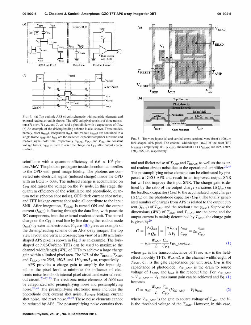
FIG. 4. (a) Top-cathode APS circuit schematic with parasitic elements andexternal readout circuit is shown. The APS unit pixel consists of three transis-tors (TRESET, TREAD, and TAMP) and a photodiode with a capacitance of CPD.(b) An example of the driving/reading scheme is also shown. Three modes,namely, reset (treset), integration (tint), and readout (tread) are contained in asingle frame. tamp and thold are the switched-capacitor amplifier ON time andreadout signal hold time, respectively. VBIAS, VDD, and VREF are constantvoltage biases; VSW is used to reset the charge on CFB after output chargereadout.
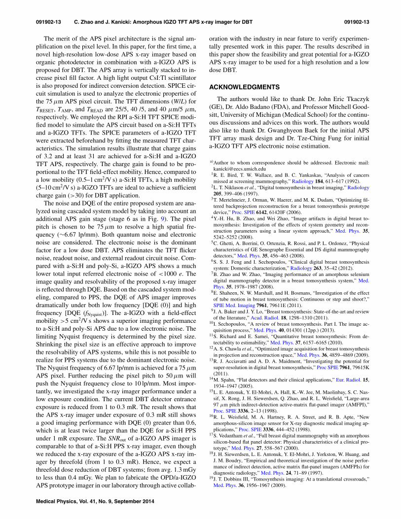
scintillator with a quantum efficiency of 6.6 × 10⁴ pho-tons/MeV. The photons propagate inside the columnar needlesto the OPD with good image fidelity. The photons are con-verted into electrical signal (induced charge) inside the OPDwith an EQE > 60%. The induced charge is accumulated onCPD and raises the voltage on the VS node. In this stage, thequantum efficiency of the scintillator and photodiode, quan-tum noise (photon shot noise), OPD dark current shot noise,and TFT leakage current shot noise all contribute to the inputSNR. After integration, TREAD is turned ON and the outputcurrent (IOUT) is flowing through the data line, with parasiticRC components, into the external readout circuit. The storedcharge on the CFB is read line by line during the readout mode(tread) by external electronics. Figure 4(b) gives an example ofthe driving/reading scheme of an APS x-ray imager. The topview layout and vertical cross-section view of a 100 μm fork-shaped APS pixel is shown in Fig. 5 as an example. The fork-shaped or half-Corbino TFTs can be used to maximize thechannel width/length (W/L) of TFTs to achieve a large chargegain within a limited pixel area. The W/L of the TRESET, TAMP,and TREAD are 25/5, 150/5, and 150 μm/5 μm, respectively.
APS provides a charge gain to amplify the input sig-nal on the pixel level to minimize the influence of elec-tronic noise from both internal pixel circuit and external read-out circuit.20–22, 25 The electronic noise elements of APS canbe categorized into preamplifying noise and postamplifyingnoise.20, 49 The preamplifying electronic noise includes thephotodiode dark current shot noise, TRESET leakage currentshot noise, and reset noise.20, 49 These noise elements cannotbe reduced by APS. The postamplifying noise contains ther-
FIG. 5. Top view layout (a) and vertical cross-sectional view (b) of a 100 μmfork-shaped APS pixel. The channel width/length (W/L) of the reset TFT(TRESET), amplifying TFT (TAMP), and readout TFT (TREAD) are 25/5, 150/5,150 μm/5 μm, respectively.
mal and flicker noise of TAMP and TREAD, as well as the exter-nal readout circuit noise due to the operational amplifier.20, 49
The postamplifying noise elements can be eliminated by pro-posed a-IGZO APS and result in an improved output SNRbut will not improve the input SNR. The charge gain is de-fined by the ratio of the output charge variations (�Qout) onthe feedback capacitor (CFB) to the accumulated input charges(�Qin) on the photodiode capacitor (CPD). The totally gener-ated number of charges from APS is related to the output cur-rent (IOUT) of TAMP and the readout time (tread). Suppose thedimensions (W/L) of TAMP and TREAD are the same and theoutput current is mainly determined by TAMP, the charge gainis given by20
G =∣∣∣∣�Qout
�Qin
∣∣∣∣ =∣∣∣∣�IOUT
�VS
∣∣∣∣ tread
CPD= gm
tread
CPD
= μeffWAMP
L
Cox
CPDVDS_AMPtread, (1)
where gm is the transconductance of TAMP, μeff is the field-effect mobility TFTs, WAMP/L is the channel width/length ofTAMP, Cox is the gate capacitance per unit area, CPD is thecapacitance of photodiode, VDS_AMP is the drain to sourcevoltage of TAMP, and tread is the readout time. For VDS_AMP
> VGS_AMP − VT, maximum gain can be achieved and Eq. (1)becomes
G = μeffWAMP
L
Cox
CPD(VGS_AMP − VT)tread, (2)
where VGS_AMP is the gate to source voltage of TAMP and VT
is the threshold voltage of the TAMP. However, in this case,
Medical Physics, Vol. 41, No. 9, September 2014

091902-6 C. Zhao and J. Kanicki: Amorphous IGZO TFT APS x-ray imager for DBT 091902-6
TABLE II. List of parameters, driving scheme, driving voltages, and TFTdimensions used in SPICE simulation.
Parameter Value
Pixel pitch (apix) 75 μmPhotodiode capacitance (CPD) 1 pFFeedback capacitance (CFB) 100 pFVBIAS 15 VVREF 10 VVDD 5 VVRESET (OFF/ON) −3 V/15 VVREAD (OFF/ON) −3 V/15 VVT 5 VTAMP (W/L) 40 μm/5 μmTREAD (W/L) 40 μm/5 μmTRST (W/L) 25 μm/5 μmReset time (treset) 7 msCharge integration time (tint) 10 msIntegrator ON time (tamp) 40 μsReadout time (tread) 20 μsHold time (thold) 10 μsFrame time (tframe) 145 ms
the gain is not a constant and the output to input signal is notlinear, since VS and VGS_AMP are increasing during light in-tegration. Therefore, TAMP is preferred to work in the linearregion (VDS_AMP < VGS_AMP − VT) to maintain linearity be-tween input and output signals. As shown in Table II, in thesimulation, VS is between VREF (10 V after reset) and VBIAS
(15 V for fully charged CPD), VDD and VT are 5 V. For thisspecific operating condition, we have VDD < VS − VT, henceVDS_AMP < VGS_AMP − VT, which is linear region condition.
To achieve a large charge gain, two TFT parameters needto be optimized based on Eq. (1). First, the value of TFT chan-nel width/length (WAMP/L) should be large. For high resolu-tion x-ray imagers (e.g., 3200 × 4000 with a pixel pitch of75 μm), the dimension of TFT (WAMP/L of TAMP ∼ 40 μm/5 μm) is limited by the small pixel size. In this case, the fork-shaped50 (Fig. 5) or half-Corbino51 TFT structure is a pos-sible approach to achieve large WAMP/L within a small pixelarea. Second, a high TFT field-effect mobility (μeff) must beused to achieve a large charge gain without enlarging the TFTdimensions and pixel size. Third, the readout time can be re-duced using high mobility TFT technology combined with theindirect detector. Consequently, the reduced total scan timeleads to reduced human motion and low dose if continuousx-ray illumination is used.
To evaluate the feasibility of different TFT technologiesand optimize the pixel circuit design for proposed APS x-ray imager at the early stage, SPICE simulation is a powerfultool. In Sec. 3.B, the electrical properties of the APS pixel andreadout circuits will be investigated. The charge gain can beextracted from simulation results.
3.B. Active pixel sensor pixel circuit simulation
The SPICE circuit simulations were performed using SIL-VACO SmartSpice simulator. First, the a-Si:H TFT character-
istics were model by RPI a-Si TFT model.29 Then the RPI a-SiTFT model was modified for a-IGZO TFTs. SPICE parame-ters of a-IGZO TFT were extracted by fitting the calculatedcurves to experimental measured TFT current–voltage (I–V)characteristics.52 We used the SPICE model of diode in com-bination with a current source and photodiode capacitance forthe OPD. The SPICE model for the switched-capacitor ampli-fier (Burr-Brown ACF2101) provided by the supplier53 wasalso integrated in the circuit simulation. The electronic noiseis not included in the simulation and will be discussed numer-ically in Sec. 3.C.
We first simulated the APS pixel circuit performance basedon a-Si:H TFTs. The switched-capacitor amplifier is firstturned ON and then the readout TFT (TREAD) is ON for20 μs.25 All the simulation parameters, TFT dimensions anddriving scheme25 referring to Fig. 4(b) are listed in Table II.The pixel pitch (apix) is 75 μm, which is used to achieve ahigh Nyquist frequency (∼6.67 lp/mm). Smaller pixel size(e.g., 50 μm) can restrict the TFT dimensions (W/L), andcharge gain. It also requires longer image acquisition timeand larger storage space for the data file. Compared to the100 μm pixel pitch, the total effective channel area of TAMP
and TREAD for a 75 μm pixel will shrink from 2 × 30 μm ×50 μm to 2 × 20 μm × 20 μm using the fork-shaped TFTstructure. Hence the W/L of TAMP and TREAD is normalizedto 40 μm/5 μm. CPD is around 1 pF, which corresponds to theproposed organic photodiode capacitance of a single pixel;25
if CPD is reduced, the gain will increase, but the dynamicrange will be reduced.
Figure 6(a) shows the simulated output voltage (VOUT) fora-Si:H APS, based on the proposed readout scheme. It can beseen that during the readout time (20 μs), a photocurrent (Iph)from 0.01 to 0.5 nA can be detected. To optimize the pixeldesign, different channel widths of TAMP and TREAD (WAMP
and WREAD) were investigated with the channel length fixed to5 μm (LAMP = LREAD = 5 μm) [Fig. 6(b)]. The output chargeis defined as the variance between the integrated charge on theamplifier under illumination and dark condition. First, whenwe set WAMP = WREAD to be 40, 30, and 20 μm, the resultsindicate that the charge gain is proportional to the transistorchannel width. Second, by considering a constant pixel areaof 75 × 75 μm, the sum of channel widths of TAMP and TREAD
(WAMP + WREAD) is 80 μm. Charge gain of 3.2, 2.8, and 2.1 isachieved for WAMP/WREAD equals to 40/40, 50/30, and 60/20,respectively. The result illustrates that maximum charge gaincan be achieved, when WAMP and WREAD match each other.The maximum detectable charge is 5 pC, as determined byCPD(VBIAS − VREF). The maximum charge gain of the 75 μma-Si:H TFT-based APS is only 3.2, which is insufficient forsignal amplification and noise reduction needed for next gen-eration DBT as demonstrated in Sec. 4.B. The small chargegain is mainly due to the low TFT field effect mobility (0.5–1 cm2/V s). The limitations of low mobility a-Si:H APS are ahigh electronic noise, a long readout time, and a high dose.The charge gain can be improved by increasing the TFT field-effect mobility [Eq. (1)] without affecting the pixel size andimage resolution. Thereby, a high mobility TFT technology isrequired to go beyond a-Si:H TFTs.
Medical Physics, Vol. 41, No. 9, September 2014

091902-7 C. Zhao and J. Kanicki: Amorphous IGZO TFT APS x-ray imager for DBT 091902-7
FIG. 6. (a) Simulated a-Si:H TFT APS circuit output voltage under differentphotocurrent levels; (b) output charge and gain using different channel widths(WAMP and WREAD) of TAMP and TREAD, while the length of the TFTs isconstant (LAMP = LREAD = 5 μm), are shown.
a-IGZO TFT technology is an ideal candidate for next gen-eration medical imaging because of a high field-effect mobil-ity (5–20 cm2/V s), a low flicker noise (αH ∼ 1.5 × 10⁻³),a small TFT off-current (<10−13 A), and a low-temperaturefabrication process.54, 55 The simulated output-input signalcharacteristics of a-IGZO TFT-based APS are shown inFig. 7(a) using the same driving schemes as shown inFig. 4(b). We change the field-effect mobility value from 5to 20 cm2/V s [which can be easily realized by amorphousmetal-oxide TFTs (Refs. 54–56)] to evaluate the relationshipbetween APS charge gain and TFT mobility. A charge gain ofat least 31 is achieved and the maximum value can be above100 if a large mobility (20 cm2/V s) (Ref. 56) of metal oxideTFTs is selected. Further increase in the charge gain leads tosaturation of the feedback capacitor (CFB) without additionalsignal detection. The charge gain linearly increases with a-IGZO TFT mobility as shown in Fig. 7(b), which is consistentwith Eq. (1). It is also found using simulation that if TAMP ischosen to be operating in the saturation region, the output-to-input charge signal relationship is nonlinear. To maintain thesignal linearity, we choose TAMP to be operated in the linearregion. We have already reported a fabricated a-IGZO APSwith the charge gain ∼25 (normalized to ∼30 with 75 μmpixel pitch).57 The a-IGZO TFT mobility of the fabricate APScircuit is 5.6 cm2/V s. The normalized experimental data ofboth a-Si:H (Ref. 25) and a-IGZO TFT APS (Ref. 57) are alsoplotted in Fig. 7(b). Based on both experimental and simula-tion results, the charge gain of a-IGZO TFT APS is at least×10 higher than a-Si:H TFT APS with same device and pixel
FIG. 7. (a) Simulated integrated charge signal and (b) charge gain for a-IGZO TFT active pixel sensor (solid symbol). Field-effect mobility valuesof the a-IGZO TFTs from 5 to 20 cm2/V s are used. The normalized exper-imental data (open symbol) of the a-Si:H (Ref. 25) and a-IGZO TFT APS(Ref. 57) are also compared.
dimensions. The large charge gain of a-IGZO APS can mini-mize the influence of the electronic noise.
In addition to the large charge gain achieved by a-IGZOAPS, Fung et al. reported that the low frequency flicker (1/f)noise of a-IGZO TFTs is lower compared to a-Si:H TFTs.55
The a-IGZO TFT Hooge’s parameter (αH) extracted from the1/f noise measurement is 1.5 × 10⁻³, which is comparable tothat of the poly-Si TFTs.58 Compared to the αH value of a-Si:H TFTs (3 × 10⁻³ < αH <1.2 × 10⁻²),55, 59, 60 the low αH
of a-IGZO TFTs makes them attractive for low-noise applica-tions such as DBT.
Another candidate for APS-based medical imaging systemis poly-Si TFT.21, 22 Detailed comparison of the APS pixel cir-cuit electronic noise using a-Si:H, poly-Si, and a-IGZO TFTtechnologies is discussed in Sec. 3.C.
3.C. APS pixel circuit electronic noise
Each electronic noise element is modeled and calculatedbased on reported APS noise model developed by Karimet al.20 First, the OPD dark current shot noise is given by49
σPD,shot =√
Idarktframe/q, (3)
Medical Physics, Vol. 41, No. 9, September 2014

091902-8 C. Zhao and J. Kanicki: Amorphous IGZO TFT APS x-ray imager for DBT 091902-8
where Idark (∼4.89 × 10⁻¹³ A) is the dark current of OPD(calculated using the dark current density of 10−8 A/cm2, apixel pitch of 75 μm, and fill factor of 0.87) and tframe is theframe time (145 ms).
Similarly, the TRESET leakage current shot noise is givenby49
σTFT,shot =√
Iofftframe/q, (4)
where Ioff is the TFT leakage current (off-current). Leakagecurrent of 10−12, 2 × 10⁻¹², and 5 × 10⁻¹⁴ A is used for a-Si:H, poly-Si, and a-IGZO TFTs, respectively.50, 54, 61
If double sampling is implemented, the reset noise for APSis given by49
σreset = √2kT Cpix/q, (5)
where k is the Boltzmann constant, T is the Kelvin tempera-ture, and Cpix (∼1 pF) is the input pixel capacitance, which isdominated by CPD.
The input referred preamplifying pixel noise, which cannotbe removed by APS, is given by
σpre-AMP =√
σPD,shot2 + σTFT,shot
2 + σreset2. (6)
In this work, since both the TAMP and TREAD operate inthe linear region, the noise power spectral density of thermalnoise for TAMP and TREAD is given by55
SThermal = 4kT μeffCox (W/L) (VGS − VT) , (7)
where k is the Boltzmann constant, T is the Kelvin tempera-ture, Cox is the gate capacitance per unit area (∼17 nF/cm2),W, L, and VGS are the channel width, length, and the gate tosource voltages of TAMP and TREAD, and VT is the TFT thresh-old voltage (∼5 V in the simulation). All the driving voltagesand device dimension parameters can be found in Table II.The corresponding thermal noise equivalent electrons of TAMP
and TREAD (σ Thermal,AMP and σ Thermal,READ) can be calculatedby integrating the noise power spectral density over the noisebandwidth of a first-order low-pass filtering circuit using themethod and equations developed by Karim et al.20 The noisecalculation for TAMP is modified for linear region operation.
The noise power spectral density of flicker noise for TAMP
and TREAD operating both in the linear region are given by55
SFlicker = αHqμeffCoxW (VGS − VT)V 2DS
f L3, (8)
where αH is the Hooge’s parameter (αH equals to 10−2,10−3, and 1.5 × 10⁻³ for a-Si:H, poly-Si, and a-IGZO TFTs,respectively),55, 58–60 VGS and VDS are the gate to source volt-age and drain to source voltage of TAMP and TREAD, and f is thefrequency. The flicker noise equivalent electrons σ Flicker,AMP
and σ Flicker,READ can be calculated by integrating the noisespectral density over frequency adopted from the model de-veloped by Karim et al.20
The external readout circuit noise (σ amp) is mainly gen-erated by the switched-capacitor amplifier. The readout cir-cuit noise can be modeled as having a fixed noise componentof the amplifier (σ amp0) in addition to capacitance dependentcomponent (δCd) (Refs. 20 and 62)
σamp = σamp0 + δCd, (9)
where σ amp and δ are an amplifier’s characteristic constants.Cd is the capacitance loading at the amplifier’s input node,which mainly includes the capacitance on the data line, CDATA
[Fig. 4(a)]. For the specific low-noise amplifier, σ amp0 and δ
are found to be 250 e and as 15 e/pF, respectively.20 The dom-inant contribution to CDATA is the total parasitic capacitancefrom the overlap area between each gate line and data line.CDATA is typically in the order of 100 pF.20, 62
The output referred postamplifying pixel noise is givenby
σpost-AMP,out =√
σThermal,AMP2 + σThermal,READ
2 + σFlicker,AMP2 + σFlicker,READ
2 + σamp2. (10)
The input referred postamplifying pixel noise, which canbe significantly reduced by APS, is given by output referredpostamplifying pixel noise divided by the APS charge gain(σ post-AMP,in = σ post-AMP,out/G). Finally, the total input referrednoise is given by the square root of the quadratic sum of theinput referred preamplifying and postamplifying noise.
We are comparing the input referred noise equivalent elec-trons for a-Si:H, poly-Si, and a-IGZO APS in Fig. 8. All thenoise elements discussed above are included in the calcula-tion. The photodiode dark current density is 10−8 A/cm2 re-ferring to that of OPD,23 which is used for a-Si:H, poly-Si,and a-IGZO APS. The mobility of a-Si:H, poly-Si, and a-IGZO TFTs is set to be 0.5, 100, and 10 cm2/V s, correspond-ing to charge gains of 3.3, 664, and 69 for a 75 μm pixel
pitch, respectively. The calculated charge gain is consistentwith that of SPICE simulation. The calculated total input re-ferred noise for a-Si:H, poly-Si, and a-IGZO APS is 2178,1618, and 912 e, respectively.
First, for a-Si:H APS, as shown in Fig. 8, both the pream-plifying noise and postamplifying noise are significant. Thepreamplifying noise is dominated by the TFT leakage currentshot noise of TRESET (952 e) due to the high leakage currentof ∼10−12 A. It is demonstrated that the postamplifying noiseof a-Si:H APS remains high because of a low field-effect mo-bility (∼0.5 cm2/V s) and a low charge gain (∼3). Therefore,the total electronic pixel circuit noise of a-Si:H APS is high.The a-Si:H TFT APS cannot be used for DBT because of itslow carrier mobility, limited charge gain, and large threshold
Medical Physics, Vol. 41, No. 9, September 2014

091902-9 C. Zhao and J. Kanicki: Amorphous IGZO TFT APS x-ray imager for DBT 091902-9
FIG. 8. Calculated input referred noise equivalent electrons of all noise ele-ments for a-Si:H, poly-Si, and a-IGZO APS. The mobility of a-Si:H, poly-Si,and a-IGZO TFTs is set to be 0.5, 100, and 10 cm2/V s, corresponding tocharge gains of 3.3, 664, and 69, respectively. Leakage current of 10−12, 2× 10⁻¹², and 5 × 10⁻¹⁴ A are used for a-Si:H, poly-Si, and a-IGZO TFTs,respectively. The photodiode dark current is 10−8 A/cm2, referring to the ex-perimental data of OPD. The frame time is 145 ms.
voltage shift63 during operation. Izadi et al. optimized the a-Si:H APS using theoretical calculations and reported total in-put referred noise of <1000 e.64 To achieve such low value, asmall pixel capacitance of <100 fF has to be used to achieve alarger charge gain for a-Si:H APS. However, such low capac-itance value is not suitable for DBT due to the dominating ca-pacitance of OPD (∼1 pF) and will result in a limited dynamicrange owning to a small maximum detectable signal. For typ-ical DBT detectors with a pixel capacitance of ∼1 pF, theoptimized a-Si:H TFT dimension is W/L = 100 μm/5 μm.64
Therefore, we conclude that a-Si:H APS cannot be used forhigh resolution DBT due to a large TFT dimension.
For poly-Si APS, the significant charge gain (∼664) ef-fectively removes the postamplifying noise. However, a highTFT leakage current (∼2 × 10⁻¹² A) results in a high TFTleakage current shot noise (1346 e), which cannot be removedby APS. Antonuk et al. have demonstrated that there was littleimprovement in the signal-to-noise properties of poly-Si APSprototype imagers due to their high level of electronic noise.22
They claim that the grain boundaries of polysilicon containnumerous trap states, which are associated with a large leak-age current (high TFT shot noise), a high 1/f noise, and a poorelectrical property (threshold voltage, mobility, and currentleakage) uniformity.22 The imaging performance of fabricatedpoly-Si APS array is consistent with our noise modeling re-sults. Because the polycrystalline nature cannot be modified,the poor SNR will prevent poly-Si APS to be used for DBTusing existing poly-Si TFT technology.
As shown in Fig. 8, the minimum input referred electronicnoise is achieved by a-IGZO APS. For a-IGZO TFTs with afield-effect mobility of 10 cm2/V s, the calculated charge gainis around 69. This value is consistent with the SPICE simu-lation results in Fig. 7. The charge gain is sufficient to elim-inate the postamplifying noise (137 e). In addition, the lowoff-current of a-IGZO TFTs (5 × 10⁻¹⁴ A) (Ref. 48) reduces
the preamplifying noise (901 e). The total noise is only 912 e,which is suitable for low-dose DBT. The a-IGZO APS totalelectronic noise can be further reduced to 658 e if the OPDdark current is reduced to 10−9 A/cm2. The APS noise can beoptimized when the driving scheme, device structure, and lay-out are optimized for a given application such as DBT, whichis outside of the scope of this paper. Already Sony Corpora-tion demonstrated excellent a-IGZO TFT uniformity and reli-ability with a low leakage current and noise.65 Finally, the lowprocess temperature favors the fabrication of a-IGZO TFTson flexible or deformable substrates,54, 66 which is attractiveto future flexible x-ray imaging applications.67
4. NOISE AND DETECTIVE QUANTUM EFFICIENCY
4.A. Cascaded system model
To analyze the electrical performance such as noise andDQE of the a-IGZO APS AMFPI, the cascaded systemanalysis18, 30–32, 36 is an effective and reliable approach. Themodel was described in detail by Siewerdsen et al. by consid-ering the noise transfer as gain and spreading stages.18 For again stage, the noise power spectra of stage i (Si) as a functionof spatial frequency is determined by the average gain (gi),the mean fluence of input quanta (qi−1), gain variance (σ gi),and additional electronic noise element in the stage (Sadd),18
Si(u, v) = gi2Si−1(u, v) + σ 2
giqi−1 + Saddi
(u, v). (11)
The spreading stages represent the image blurring due toinput quanta spreading over the spatial frequency in two di-mensions. For a stochastic spreading stage, the input signal isblurred due to light scattering. This is the case for the scin-tillator scattering effect. The noise transfer for a stochasticspreading stage is18
Si(u, v) = [Si−1(u, v) − qi−1
]T 2
i (u, v) + qi−1, (12)
where qi−1 represents the uncorrelated component that is notaffected by the spreading stage, and Ti(u,v) is the MTF ofthe ith stage. On the other hand, for a deterministic spread-ing stage, the NPS is directly blurred by a MTF,18
Si(u, v) = Si−1(u, v)T 2i (u, v). (13)
The deterministic spreading corresponds to the image blur-ring by the presampling pixel MTF in the fifth stage, T5(u,v),in the tomosynthesis system. The complete noise transfer ofthe system can be described by a series of gain and spread-ing stages modeled by the cascaded system analysis. The flowchart of the cascaded system is shown in Fig. 9.
The APS amplifies both the quantum noise and the pream-plifying electronic noise by the charge gain (g6).20 Thus, theoutput referred NPS as a function of spatial frequency of theentire DBT system in the unit of e2 mm2 can be derived tobe18
S(u, v) = (a4
pdq0g1g2g4[1 + g4
(g2 + εg2
)T 2
3 (u, v)]
× T 25 (u, v) + Spre-AMP(u, v)
)g6
2
+ Spost-AMP(u, v), (14)
Medical Physics, Vol. 41, No. 9, September 2014

091902-10 C. Zhao and J. Kanicki: Amorphous IGZO TFT APS x-ray imager for DBT 091902-10
FIG. 9. A seven-step cascaded system flow chart showing the signal andnoise transfer of APS indirect x-ray imager.
where apd is photodiode active area considering the pixelfill factor, gi and Ti are the gain and MTF of stage i, εg2
is the Poisson excess of gain stage 2, Spre-AMP and Spost-AMP
are the output referred NPS of preamplifying and postampli-fying pixel electronic noise, respectively. Both the quantumnoise (photon shot noise) and electronic noise are included inthe model. The quantum noise is given by the first term inEq. (14). The output referred individual pixel variance of thesystem can be obtained by integrating the NPS over the spatialfrequency,
σ 2tot =
⎛⎝
∫u
∫v
a4pdq0g1g2g4[1 + g4(g2 + εg2 )T 2
3 (u, v)]
×T 25 (u, v)dudv + σ 2
pre-AMP
⎞⎠ g6
2 + σ 2post-AMP. (15)
The MTF of the system is given by
T (u, v) = T3(u, v)T5(u, v), (16)
where T3 represents the MTF due to the scintillator scatteringeffect and T5 is the MTF associated with the pixel aperture.We have18
T3(u, v) ≈ 1
1 + H · (u2 + v2), (17)
T5(u, v) = ∣∣sinc(apdu) · sinc(apdv)∣∣ , (18)
where H is a parameter describing the scattering effect of thescintillator.
The DQE of the system is determined by the square ratio ofthe output SNR to the input SNR. The DQE of the proposedAPS x-ray imager is
DQE(u, v) = (SNRout)2
(SNRin)2 = d2 · T 2(u, v)
q0 · S(u, v)
= a4pdq0
[g1g2g4g6 · T (u, v)
]2
S(u, v), (19)
TABLE III. Key parameters used in the cascaded system model.
Parameters Value Description
X 10 μR to 10 mR Exposureq0/X 46 520 (Unit: x rays/mm2/mR) Mean x-ray fluenceg1 0.83 Gain of stage 1g2 520 Gain of stage 2εg2 5.26 Poisson excess of stage 2H 0.18 Scattering parameter of stage 3g4 0.6 Gain of stage 4g6 3.3–664 APS charge gain of stage 6apix 50–125 μm Pixel pitchFF(APS) 0.87 (vertically stacked) APS pixel fill factorFF(PPS) 0.45 (in-plane) PPS pixel fill factor
where SNRout and SNRin are the output and input signal-to-noise ratio, respectively, d is the mean output signal in unitof electrons, q0 is the incident x-ray fluence, and T [Eq. (16)]and S [Eq. (14)] are the MTF and NPS of the system, respec-tively. The output electrons can be converted to voltage, whichis then converted to a digital number (output digital signal).The results of the noise and DQE modeling using the cas-caded system are shown in Sec. 4.B–4.D. All the key param-eters associated with the cascaded system model are listed inTable III. The parameters associated with the x-ray sourceand the scintillator were reported by El-Mohri et al.36 cor-responding to a 26 kVp incident x-ray beam and high lightoutput (HL) CsI:Tl scintillator46 used for mammography andtomosynthesis. The scintillator deposited on a fiber optic platewas used to extract those parameters. The scintillator gainof the HL CsI:Tl is limited by the low optical transmission(∼60%) of the fiber optic plate.36 Direct deposition of theCsI:Tl scintillator on top of the OPD will achieve a high scin-tillator gain of ∼520 photons/x-ray (g2). The APS charge gainof stage 6 is 3.3, 69, and 664 for a-Si:H, a-IGZO, and poly-SiAPS, respectively. The pixel FF using the vertically stackedOPD/APS TFT backplane structure is 0.87, while the FF ofconventional in-plane PPS is ∼0.45 for a 75 μm pixel pitch.
4.B. Noise of the a-IGZO active pixel sensor imager
APS pixel circuit is proposed to reduce the total pixelnoise, which contains both the quantum noise (photon shotnoise) and electronic noise. The quantum noise and thepreamplifying APS electronic noise cannot be eliminatedby APS, while the postamplifying noise can be minimized.Figure 10 shows the input referred total pixel noise of theproposed AMFPI with a pixel pitch of 75 μm as a func-tion of exposure. The same OPD is used for all devices.The calculation is based on the cascaded system [Eq. (15)]discussed in Sec. 4.A. The input referred noise variance iscalculated by the output noise divided by the charge gain.The detector entrance exposure range is from 10 mR, whichis an average of mammography exposure, to 10 μR, whichis comparable to the exposure of normal fluoroscopy.62 Thegeneral exposure of tomosynthesis is around 1 mR.62 Wepushed the lower end of exposure to 0.1 mR to investigate the
Medical Physics, Vol. 41, No. 9, September 2014

091902-11 C. Zhao and J. Kanicki: Amorphous IGZO TFT APS x-ray imager for DBT 091902-11
FIG. 10. Input referred pixel noise of 75 μm a-Si:H, poly-Si, and a-IGZOAPS AMFPIs under exposures ranging from 10 μR to 10 mR. The a-Si:HPPS imager data are also shown. Both the quantum noise (dashed line) andelectronic noise are included. The pixel noise of the a-IGZO APS imager canbe further reduced by reducing the dark current of OPD from 10−8 to below10−9 A/cm2.
feasibility of reducing the patient dose during tomosynthesis.The performance of a-Si:H, poly-Si, and a-IGZO APS AMF-PIs is compared with that of conventional a-Si:H PPS AMFPI.The calculated electronic noise elements of a-Si:H, poly-Si,and a-IGZO APS imagers, as shown in Fig. 8, are integratedinto the cascaded system modeling. The result shows that thequantum noise is dominant for a high exposure (>1 mR) con-dition such as mammography. For a low exposure (<1 mR)condition for DBT, the noise is dominated by the electronicnoise. The total noise of a-Si:H APS imager is comparable tothat of the a-Si:H PPS imager because of its low carrier mobil-ity, which is not sufficient to reduce the APS postamplifyingelectronic noise. The poly-Si TFT leakage current results ina high preamplifying APS noise, which cannot be eliminated.The a-IGZO APS imager shows a superior noise performancecompared to a-Si:H and poly-Si APS because of a high TFTmobility (high charge gain) and a low TFT leakage current.Therefore, the proposed a-IGZO APS is suitable for low doseDBT. The APS noise can be further reduced, if the dark cur-rent of OPD can be reduced to by one order of magnitude. Asshown in Fig. 7, the reset noise becomes dominant if the OPDdark current is minimized. Based on this analysis, OPD darkcurrent in the range of 10 pA/cm2 to 1 nA/cm2 is required forDBT. In comparison, the a-Si ITO/p-i-n/Mo photodiode darkcurrent density is about 40 pA/cm2 (@ −1 V).
4.C. Detective quantum efficiency of a-IGZO activepixel sensor imager
DQE is calculated using Eq. (19) to analyze the detectorperformance. The small pixel size (75 μm), small pixel fillfactor (0.45), low tomosynthesis x-ray exposure, and largeelectronic noise result in a low DQE for conventional a-Si:HPPS imager [Fig. 11(a)]. The DQE of PPS imager is vanishingespecially for higher spatial frequency (>5 lp/mm). The issueof a low DQE for PPS imager caused by a low SNR can besolved by replacing the PPS by the APS imager. We comparethe DQE of a-Si:H, poly-Si, and a-IGZO APS AMFPIs using
FIG. 11. (a) Calculated DQE vs spatial frequency for a-Si:H PPS, a-Si:H,poly-Si, and a-IGZO APS x-ray imagers. The influence of OPD dark currenton DQE is investigated. (b) DQE vs TFT field-effect mobilities at zero spa-tial frequency [DQE (0)] and Nyquist frequency [DQE (fNyquist)] are shown.The APS charge gain variation for TFT field-effect mobility from 0.5 to10 cm2/V s is also shown.
the same OPD vertically stacked on top of the TFT backplaneresulting in a FF of 0.87. The proposed a-IGZO APS imagershows excellent DQE values at both zero spatial frequency[DQE (0)] and at Nyquist frequency [DQE(fNyquist)] due toits low pixel noise (<1000 e) and significant signal. FromFig. 11(b), DQE (0) and DQE(fNyquist) both increase with TFTfield-effect mobility. Both DQE(0) and DQE(fNyquist) saturateif TFTs with field-effect mobility of 5 cm2/V s are used. Thiscan be easily achieved using proposed a-IGZO TFTs. The cor-responding charge gain for μeff = 5 cm2/V s is ∼30 as shownby both simulation and experimental57 results. DQE(fNyquist)is around 0.2, which demonstrates that the Nqyuist frequencyof ∼6.67 lp/mm can be resolved using a 75 μm a-IGZO APSx-ray imaging system. The imaging performance can be fur-ther improved if the dark current of OPD can be reduced. Thehigh DQE for spatial frequencies from zero to fNyquist makesa-IGZO APS an excellent candidate for next generation highresolution DBT imagers.
The limiting resolution of detectors is determined by theNyquist frequency that is influenced by the pixel size. TheNyquist frequency can be improved from ∼5 to ∼6.67 lp/mm,if a 75 μm APS pixel pitch is used. To further improve theresolution to ∼10 lp/mm, the pixel size has to be decreasedto 50 μm. The calculated MTFs with different pixel pitch areshown in Fig. 12(a). The MTF at higher spatial frequency im-proves for smaller pixel size. Both the scintillator blurring
Medical Physics, Vol. 41, No. 9, September 2014

091902-12 C. Zhao and J. Kanicki: Amorphous IGZO TFT APS x-ray imager for DBT 091902-12
FIG. 12. Calculated MTF (a) and DQE (b) for a-IGZO APS (μeff =10 cm2/V s) imager vs spatial frequency with pixel pitch ranging from 50 to125 μm. Obtained results are compared with the DQE of a-Si:H PPS imager.
effect [T3 as in Eq. (17)] and the pixel aperture effect [T5
as in Eq. (18)] are considered in the calculation. The DQEunder high spatial frequency for a-IGZO APS imager is plot-ted in Fig. 12(b). Obtained results demonstrate that the im-age resolution of a-IGZO APS imager can be improved by re-ducing the pixel pitch. The Nyquist frequency is ∼10 lp/mmfor a 50 μm pixel pitch. A pixel size of 75 or 50 μm is rec-ommended for DBT. However, smaller pixel pitch requiressmaller line width, which could affect large area imagers.It could be difficult to realize a large W/L within a smallpixel area (50 × 50 μm), which will result in a limited chargegain. In this case, a high mobility TFT technology such as a-InSnZnO (a-ITZO) in combination with advanced TFT struc-ture such as half-Corbino or dual-gate TFT can be used torealize a large charge gain within a small pixel area.56 Onthe contrary, simply shrinking the PPS pixel size will not in-crease the imager resolution. This is due to a high electronicnoise and a small pixel fill factor. Therefore, DQE (0) willbe reduced with no improvement in resolution of PPS imagerwith smaller pixel size. Therefore, we can conclude that spa-tial frequency above 5 lp/mm cannot be resolved using theconventional PPS imager.
4.D. Dose reduction in DBT
Today the MGD during tomosynthesis is still high (0.67–3.52 mGy) (Ref. 6) and needs to be reduced. The dose can bereduced by reducing the patient x-ray exposure. At the sametime, the detector entrance exposure (x-ray impinging the de-tector surface after travelling through the patient) will also bereduced accordingly. We explore the a-Si:H PPS and a-IGZOAPS imaging performance under a low detector entrance ex-posure (<1 mR). In Fig. 13(a), DQE variation of APS AMFPI
FIG. 13. Calculated DQE (a) and output SNR (b) for a-IGZO APS and a-Si:H PPS imagers vs spatial frequency under detector entrance exposure from0.3 to 1 mR.
for x-ray exposure ranging from 0.1 to 1 mR is shown. Thefield-effect mobility of a-IGZO is 10 cm2/V s. For comparisonpurpose, the data for a-Si:H PPS are also shown. The currentDBT exposure (∼ 1 mR) can be reduced to 0.3 mR without asignificant reduction of the DQE using the a-IGZO APS im-ager. The DQE of a-IGZO APS imager under a low exposure(0.3 mR) is at least 2× greater than that of a-Si PPS imagerunder a standard DBT exposure (1 mR). The image quality ofx-ray imager is determined by the output signal-to-noise ratio(SNRout) as shown in Eq. (13). Figure 13(b) shows that theSNRout of the proposed APS imager under 0.3 mR is compa-rable to that of conventional PPS imager at a much higher x-ray exposure (1 mR) indicating nondegraded image quality atlow dose. In combination with recent advances in reconstruc-tion method to increase the SNRout,68 we expect that the pa-tient dose can be reduced by threefold from ∼1.3 mGy (avg.)to 0.4 mGy for proposed x-ray imager. However, the dose can-not be reduced using the a-Si:H PPS based x-ray detector be-cause of a poor DQE and SNRout at low dose (<1 mR).
5. DISCUSSION AND CONCLUSION
Conventional a-Si:H TFT PPS is suitable for mammogra-phy due to a high x-ray exposure (10 mR) for a single pro-jection. However, for the multiprojection DBT, the averageexposure for a single projection is reduced to around 1 mRto keep overall exposure comparable to mammography. Theelectronic noise is significant for a small pixel size and alow dose conditions. To detect the small signal, the pixel sizeis limited to around 100 μm and cannot be further reduced.Moreover, the x-ray exposure for current DBT products ishigh, which leads to a high patient dose during tomosynthesis.
Medical Physics, Vol. 41, No. 9, September 2014
091902-13 C. Zhao and J. Kanicki: Amorphous IGZO TFT APS x-ray imager for DBT 091902-13
The merit of the APS pixel architecture is the signal am-plification on the pixel level. In this paper, for the first time, anovel high-resolution low-dose APS x-ray imager based onorganic photodetector in combination with a-IGZO APS isproposed for DBT. The APS array is vertically stacked to in-crease pixel fill factor. A high light output CsI:Tl scintillatoris also proposed for indirect conversion detection. SPICE cir-cuit simulation is used to analyze the electronic properties ofthe 75 μm APS pixel circuit. The TFT dimensions (W/L) forTRESET, TAMP, and TREAD are 25/5, 40 /5, and 40 μm/5 μm,respectively. We employed the RPI a-Si:H TFT SPICE modi-fied model to simulate the APS circuit based on a-Si:H TFTsand a-IGZO TFTs. The SPICE parameters of a-IGZO TFTwere extracted beforehand by fitting the measured TFT char-acteristics. The simulation results illustrate that charge gainsof 3.2 and at least 31 are achieved for a-Si:H and a-IGZOTFT APS, respectively. The charge gain is found to be pro-portional to the TFT field-effect mobility. Hence, compared toa low mobility (0.5–1 cm2/V s) a-Si:H TFTs, a high mobility(5–10 cm2/V s) a-IGZO TFTs are ideal to achieve a sufficientcharge gain (>30) for DBT application.
The noise and DQE of the entire proposed system are ana-lyzed using cascaded system model by taking into account anadditional APS gain stage (stage 6 as in Fig. 9). The pixelpitch is chosen to be 75 μm to resolve a high spatial fre-quency (∼6.67 lp/mm). Both quantum noise and electronicnoise are considered. The electronic noise is the dominantfactor for a low dose DBT. APS eliminates the TFT flickernoise, readout noise, and external readout circuit noise. Com-pared with a-Si:H and poly-Si, a-IGZO APS shows a muchlower total input referred electronic noise of <1000 e. Theimage quality and resolvability of the proposed x-ray imageris reflected through DQE. Based on the cascaded system mod-eling, compared to PPS, the DQE of APS imager improvesdramatically under both low frequency [DQE (0)] and highfrequency [DQE (fNyquist)]. The a-IGZO with a field-effectmobility >5 cm2/V s shows a superior imaging performanceto a-Si:H and poly-Si APS due to a low electronic noise. Thelimiting Nyquist frequency is determined by the pixel size.Shrinking the pixel size is an effective approach to improvethe resolvability of APS systems, while this is not possible torealize for PPS systems due to the dominant electronic noise.The Nyquist frequency of 6.67 lp/mm is achieved for a 75 μmAPS pixel. Further reducing the pixel pitch to 50 μm willpush the Nyquist frequency close to 10 lp/mm. Most impor-tantly, we investigated the x-ray imager performance under alow exposure condition. The current DBT detector entranceexposure is reduced from 1 to 0.3 mR. The result shows thatthe APS x-ray imager under exposure of 0.3 mR still showsa good imaging performance with DQE (0) greater than 0.6,which is at least twice larger than the DQE for a-Si:H PPSunder 1 mR exposure. The SNRout of a-IGZO APS imager iscomparable to that of a-Si:H PPS x-ray imager, even thoughwe reduced the x-ray exposure of the a-IGZO APS x-ray im-ager by threefold (from 1 to 0.3 mR). Hence, we expect athreefold dose reduction of DBT systems; from avg. 1.3 mGyto less than 0.4 mGy. We plan to fabricate the OPD/a-IGZOAPS prototype imager in our laboratory through active collab-
oration with the industry in near future to verify experimen-tally presented work in this paper. The results described inthis paper show the feasibility and great potential for a-IGZOAPS x-ray imager to be used for a high resolution and a lowdose DBT.
ACKNOWLEDGMENTS
The authors would like to thank Dr. John Eric Tkaczyk(GE), Dr. Aldo Badano (FDA), and Professor Mitchell Good-sitt, University of Michigan (Medical School) for the continu-ous discussions and advices on this work. The authors wouldalso like to thank Dr. Gwanghyeon Baek for the initial APSTFT array mask design and Dr. Tze-Ching Fung for initiala-IGZO TFT APS electronic noise estimation.
a)Author to whom correspondence should be addressed. Electronic mail:[email protected]
1R. E. Bird, T. W. Wallace, and B. C. Yankaskas, “Analysis of cancersmissed at screening mammography,” Radiology 184, 613–617 (1992).
2L. T. Niklason et al., “Digital tomosynthesis in breast imaging,” Radiology205, 399–406 (1997).
3T. Mertelmeier, J. Orman, W. Haerer, and M. K. Dudam, “Optimizing fil-tered backprojection reconstruction for a breast tomosynthesis prototypedevice,” Proc. SPIE 6142, 61420F (2006).
4Y.-H. Hu, B. Zhao, and Wei Zhao, “Image artifacts in digital breast to-mosynthesis: Investigation of the effects of system geometry and recon-struction parameters using a linear system approach,” Med. Phys. 35,5242–5252 (2008).
5C. Ghetti, A. Borrini, O. Ortenzia, R. Rossi, and P. L. Ordonez, “Physicalcharacteristics of GE Senographe Essential and DS digital mammographydetectors,” Med. Phys. 35, 456–463 (2008).
6S. S. J. Feng and I. Sechopoulos, “Clinical digital breast tomosynthesissystem: Domestic characterization,” Radiology 263, 35–42 (2012).
7B. Zhao and W. Zhao, “Imaging performance of an amorphous seleniumdigital mammography detector in a breast tomosynthesis system,” Med.Phys. 35, 1978–1987 (2008).
8E. Shaheen, N. W. Marshall, and H. Bosmans, “Investigation of the effectof tube motion in breast tomosynthesis: Continuous or step and shoot?,”SPIE Med. Imaging 7961, 79611E (2011).
9J. A. Baker and J. Y. Lo, “Breast tomosynthesis: State-of-the-art and reviewof the literature,” Acad. Radiol. 18, 1298–1310 (2011).
10I. Sechopoulos, “A review of breast tomosynthesis. Part I. The image ac-quisition process,” Med. Phys. 40, 014301 (12pp.) (2013).
11S. Richard and E. Samei, “Quantitative breast tomosynthesis: From de-tectability to estimability,” Med. Phys. 37, 6157–6165 (2010).
12A. S. Chawla et al., “Optimized image acquisition for breast tomosynthesisin projection and reconstruction space,” Med. Phys. 36, 4859–4869 (2009).
13R. J. Acciavatti and A. D. A. Maidment, “Investigating the potential forsuper-resolution in digital breast tomosynthesis,” Proc SPIE 7961, 79615K(2011).
14M. Spahn, “Flat detectors and their clinical applications,” Eur. Radiol. 15,1934–1947 (2005).
15L. E. Antonuk, Y. El-Mohri, A. Hall, K.-W. Jee, M. Maolinbay, S. C. Nas-sif, X. Rong, J. H. Siewerdsen, Q. Zhao, and R. L. Weisfield, “Large-area97 μm pitch indirect-detection active-matrix flat-panel imager (AMFPI),”Proc. SPIE 3336, 2–13 (1998).
16R. L. Weisfield, M. A. Hartney, R. A. Street, and R. B. Apte, “Newamorphous-silicon image sensor for X-ray diagnostic medical imaging ap-plications,” Proc. SPIE 3336, 444–452 (1998).
17S. Vedantham et al., “Full breast digital mammography with an amorphoussilicon-based flat panel detector: Physical characteristics of a clinical pro-totype,” Med. Phys. 27, 558–567 (2000).
18J. H. Siewerdsen, L. E. Antonuk, Y. El-Mohri, J. Yorkston, W. Huang, andJ. M. Boudry, “Empirical and theoretical investigation of the noise perfor-mance of indirect detection, active matrix flat-panel imagers (AMFPIs) fordiagnostic radiology,” Med. Phys. 24, 71–89 (1997).
19J. T. Dobbins III, “Tomosynthesis imaging: At a translational crossroads,”Med. Phys. 36, 1956–1967 (2009).
Medical Physics, Vol. 41, No. 9, September 2014

091902-14 C. Zhao and J. Kanicki: Amorphous IGZO TFT APS x-ray imager for DBT 091902-14
20K. S. Karim, A. Nathan, and J. A. Rowlands, “Amorphous silicon activepixel sensor readout circuit for digital imaging,” IEEE Trans. Electron Dev.50, 200–208 (2003).
21M. Koniczek, Y. El-Mohri, L. E. Antonuk, A. Liang, Q. Zhao, and H. Jiang,“Noise performance limits of advanced X-ray imagers employing poly-Si-based active pixel architectures,” Proc. SPIE 7961, 79610P (2011).
22Y. El-Mohri, L. E. Antonuk, M. Koniczek, Q. Zhao, Y. Li, R. A. Street, andJ.-P. Lu, “Active pixel imagers incorporating pixel-level amplifiers basedon polycrystalline-silicon thin-film transistors,” Med. Phys. 36, 3340–3355(2009).
23F. Arca, E. Kohlstädt, S. F. Tedde, P. Lugli, and O. Hayden, “Large ac-tive area organic photodiodes for short-pulse X-ray detection,” IEEE Trans.Electron Dev. 60, 1663–1667 (2013).
24S. F. Tedde, J. Kern, T. Sterzl, J. Fürst, P. Lugli, and O. Hayden, “Fullyspray coated organic photodiodes,” Nano Lett. 9, 980–983 (2009).
25S. F. Tedde, E. S. Zaus, J. Fürst, D. Henseler, and P. Lugli, “Active pixelconcept combined with organic photodiode for imaging devices,” IEEEElectron Dev. Lett. 28, 893–895 (2007).
26J. W. Kingsley, S. J. Weston, and D. G. Lidzey, “Stability of X-ray detec-tors based on organic photovoltaic devices,” IEEE J. Sel. Top. QuantumElectron. 16, 1770–1774 (2010).
27R. A. Street, X. D. Wu, R. Weisfield, S. Ready, R. Apte, M. Ngyuen,W. B. Jackson, and P. Nylen, “Two-dimensional amorphous silicon imagesensor array,” J. Non-Cryst. Solid 198–200, 1151–1154 (1996).
28J. T. Rahn, F. Lemmi, J. P. Lu, P. Mei, R. B. Apte, R. A. Street, R. Lujan,R. L. Weisfield, and J. A. Heanue, “High resolution x-ray imaging usingamorphous silicon flat-panel arrays,” IEEE Trans. Nucl. Sci. 46, 457–461(1999).
29M. S. Shur, H. C. Slade, M. D. Jacunski, A. A. Owusu, and T. Ytterdal,“SPICE models for amorphous silicon and polysilicon thin film transis-tors,” J. Elecrochem. Soc. 144, 2833–2839 (1997).
30I. A. Cunningham, M. S. Westmore, and A. Fenster, “A spatial-frequencydependent quantum accounting diagram and detective quantum efficiencymodel of signal to noise propagation in cascaded imaging systems,” Med.Phys. 21, 417–427 (1994).
31I. A. Cunningham and R. Shaw, “Signal-to-noise optimization of medicalimaging systems,” J. Opt. Soc. Am. A 16, 621–632 (1999).
32J. H. Siewerdsen, L. E. Antonuk, Y. El-Mohri, J. Yorkston, W. Huang, andI. A. Cunningham, “Signal, noise power spectrum, and detective quantumefficiency of indirect-detection flat-panel imagers for diagnostic radiology,”Med. Phys. 25, 614–628 (1998).
33S. O. Kasap and J. A. Rowlands, “Direct-conversion flat-panel X-ray imagesensor for digital radiography,” Proc. IEEE 90, 591–604 (2002).
34W. Zhao and J. A. Rowlands, “X-ray imaging using amorphous selenium:Feasibility of a flat panel self-scanned detector for digital radiology,” Med.Phys. 22, 1595–1604 (1995).
35J. P. Moy, “Image quality of scintillator based X-ray electronic imagers,”Proc. SPIE 3336, 14–23 (1998).
36Y. El-Mohri, L. E. Antonuk, Q. Zhao, Y. Wang, Y. Lin, H. Du, andA. Sawant, “Performance of a high fill factor, indirect detection prototypeflat panel imager for mammography,” Med. Phys. 34, 315–327 (2007).
37W. Zhao, D. Li, A. Reznik, B. J. M. Lui, D. C. Hunt, J. A. Rowlands,Y. Ohkawa, and K. Tanioka, “Indirect flat-panel detector with avalanchegain: Fundamental feasibility investigation for SHARP-AMFPI (scintilla-tor HARP active matrix flat panel imager),” Med. Phys. 32, 2954–2966(2005).
38R. C. Ronda, Luminescence: From Theory to Applications (Wiley, NewYork, 2007), pp. 105–132.
39T. Hase et al., Phosphor Handbook (CRC, 2000), pp. 539–547.40S. R. Forrest, “The path to ubiquitous and low-cost organic electronic
appliances on plastic,” Nature (London) 428, 911–918 (2004).41G. Yu, K. Pakbaz, and A. J. Heeger, “Semiconducting polymer diodes:
Large size, low cost photodetectors with excellent visible-ultraviolet sensi-tivity,” Appl. Phys. Lett. 64, 3422–2424 (1994).
42T. N. Ng, W. S. Wong, M. L. Chabinyc, S. Sambandan, and R. A. Street,“Flexible image sensor array with bulk heterojunction organic photodiode,”Appl. Phys. Lett. 92, 213303 (2008).
43B. Park, Y. H. Huh, and M. Kim, “Surfactant additives for improved pho-tovoltaic effect of polymer solar cells,” J. Mater. Chem. 20, 10862–10868(2010).
44B. C. Grabmaier, “Crystal scintillator,” IEEE Trans. Nucl. Sci. 31, 372–376(1984).
45R. A. Street, S. Nelson, L. Antonuk, and V. Perez Mendez, “Amorphous
silicon sensor arrays for radiation imaging,” Mater. Res. Soc. Symp. Proc.192, 441–452 (1992).
46Hamamatsu Corp., “FOS (fiber optic plate with scintillator) for digital X-ray imaging,” Technical Information (Hamamatsu, February 1996).
47W. Zhao, G. Ristic, and J. A. Rowlands, “X-ray imaging performance ofstructured cesium iodide scintillators,” Med. Phys. 31, 2594–2605 (2004).
48B. Ren, C. Ruth, J. Stein, A. Smith, I. Shaw, and Z. Jing, “Design andperformance of the prototype full field breast tomosynthesis system withselenium based flat panel detector,” Proc. SPIE 5745, 550–561 (2005).
49M. H. Izadi, K. S. Karim, A. Nathan, and J. A. Rowlands, “Low-noise pixelarchitecture for advanced diagnostic medical x-ray imaging applications,”Proc. SPIE 6142, 61420T (2006).
50H. Lee, G. Yoo, J.-S. Yoo, and J. Kanicki, “Asymmetric electrical prop-erties of fork a-Si:H thin-film transistor and its applications to flat paneldisplays,” J. Appl. Phys. 105, 124522 (2009).
51H. Lee, C.-H. Liu, and J. Kanicki, “Asymmetric electrical properties ofhalf Corbino hydrogenated amorphous silicon thin-film transistor and itsapplications to flat panel displays,” Jpn. J. Appl. Phys. 50, 074203 (2011).
52C. Chen, K. Abe, T.-C. Fung, H. Kumomi, and J. Kanicki, “AmorphousIn-Ga-Zn-O thin film transistor current-scaling pixel electrode circuit toactive-matrix organic light-emitting displays,” Jpn. J. Appl. Phys. 48,03B025 (2009).
53Texas Instruments, “ACF2101 PSpice model,” Tools and software(Texas Instruments, October 2000) (available URL: http://www.ti.com/product/acf2101).
54K. Nomura, H. Ohta, A. Takagi, T. Kamiya, M. Hirano, and H. Hosono,“Room-temperature fabrication of transparent flexible thin-film transistorsusing amorphous oxide semiconductors,” Nature (London) 432, 488–492(2004).
55T.-C. Fung, G. Baek, and J. Kanicki, “Low frequency noise in long channelamorphous In-Ga-Zn-O thin film transistors,” J. Appl. Phys. 108, 074518(2010).
56T. Arai and T. Sasaoka, “Invited paper: Emergent oxide TFT technologiesfor next-generation AM-OLED displays,” SID Symp. Digest Tech. Pap. 42,710–713 (2011).
57R. Zhang, L. Bie, T.-C. Fung, E. K.-H. Yu, C. Zhao, and J. Kanicki, “Highperformance amorphous metal-oxide semiconductors thin-film passive andactive pixel sensors,” in Proceedings of IEEE International Electron De-vices Meeting (IEDM) (IEEE, Washington, DC, 2013), pp. 667–670.
58A. Mercha, L. Pichon, R. Carin, K. Mourgues, and O. Bonnaud, “Grainboundary trap passivation in polysilicon thin film transistor investigated bylow frequency noise,” Thin Solid Films 383, 303–306 (2001).
59J. Rhayem, D. Rigaud, M. Valenza, N. Szydlo, and H. Lebrun, “1/f noisemodeling in long channel amorphous silicon thin film transistors,” J. Appl.Phys. 87, 1983–1989 (2000).
60J. N. Boudry and L. E. Antonuk, “Current-noise-power spectra of amor-phous silicon thin-film transistors,” J. Appl. Phys. 76, 2529–2534 (1994).
61S.-W. Lee, and S.-K. Joo, “Low temperature poly-Si thin-film transistorfabrication by metal-induced lateral crystallization,” IEEE Electron Dev.Lett. 17, 160–162 (1996).
62L. E. Antonuk, Q. Zhao, Y. El-Mohri, H. Du, and Y. Wang, “An investi-gation of signal performance enhancements achieved through innovativepixel design across several generations of indirect detection, active matrix,flat-panel arrays,” Med. Phys. 36, 3322–3339 (2009).
63F. R. Libsch and J. Kanicki, “Bias-stress-induced stretched-exponentialtime dependence of charge injection and trapping in amorphous thin-filmtransistors,” Appl. Phys. Lett. 62, 1286–1288 (1993).
64M. H. Izadi and K. S. Karim, “Noise optimization analysis of an activepixel sensor for low-noise real-time fluoroscopy,” IET Circuit Dev. Syst. 1,251–256 (2007).
65T. Arai, N. Morosawa, K. Tokunaga, Y. Terai, E. Fukumoto, T. Fujimori,and T. Sasaoka, “Highly reliable oxide semiconductor TFT for AMOLEDdisplays,” J. Soc. Inf. Display 19, 205–211 (2011).
66J.-S. Park, T.-W. Kim, D. Stryakhilev, J.-S. Lee, S.-G. An, Y.-S. Pyo, D.-B. Lee, Y. G. Mo, D. U. Jin, and H. K. Chung, “Flexible full color organiclight-emitting diode display on polyimide plastic substrate driven by amor-phous indium gallium zinc oxide thin-film transistors,” Appl. Phys. Lett.95, 013503 (2009).
67R. A. Lujan and R. A. Street, “Flexible X-ray detector array fabricated withoxide thin-film transistors,” IEEE Electron Dev. Lett. 33, 688–690 (2012).
68K. Michielsen, K. VanSambrouck, A. Jerebko, and J. Nuyts, “Patchworkreconstruction with resolution modeling for digital breast tomosynthesis,”Med. Phys. 40, 031105 (10pp.) (2013).
Medical Physics, Vol. 41, No. 9, September 2014