&/w l í r ïz &/w l í r ïz &/w l í r ïz
TRANSCRIPT

Jaydeep Joshi et [email protected]
TECHNOLOGIES FOR REALIZATION OF LARGE SIZE RF SOURCES FOR –VE NEUTRAL BEAM SYSTEMS FOR ITER -Challenges, experience
and path ahead
FIP/1-3Rb
FIP/1-3Ra
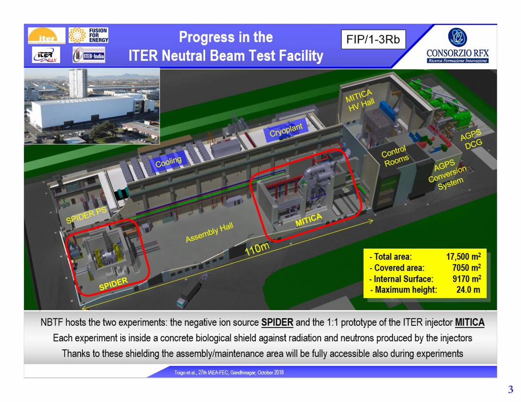
PROGRESS IN ITER NEUTRAL BEAM FACILITY Toigo et al
DEMONSTRATION OF 1 MV VACUUM INSULATION FOR THE VACUUM INSULATED
BEAM SOURCE IN THE ITER NB SYSTEM
FIP/1-3Rc
Kojima et [email protected]
Presented by: Jaydeep Joshi on behalf of FIP/1-3Ra, FIP/1-3Rb and FIP/1-3Rc
27th IAEA-FEC, Gandhinagar, October 2018
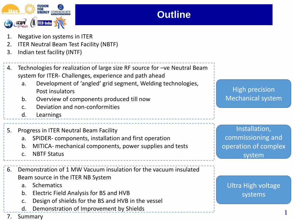
Outline
1. Negative ion systems in ITER2. ITER Neutral Beam Test Facility (NBTF)3. Indian test facility (INTF)
4. Technologies for realization of large size RF source for –ve Neutral Beamsystem for ITER- Challenges, experience and path ahead
a. Development of ‘angled’ grid segment, Welding technologies,Post insulators
b. Overview of components produced till nowc. Deviation and non-conformitiesd. Learnings
5. Progress in ITER Neutral Beam Facilitya. SPIDER- components, installation and first operationb. MITICA- mechanical components, power supplies and testsc. NBTF Status
6. Demonstration of 1 MW Vacuum insulation for the vacuum insulatedBeam source in the ITER NB System
a. Schematicsb. Electric Field Analysis for BS and HVBc. Design of shields for the BS and HVB in the vesseld. Demonstration of Improvement by Shields
7. Summary
High precision Mechanical system
Installation, commissioning and
operation of complex system
Ultra High voltage systems
1
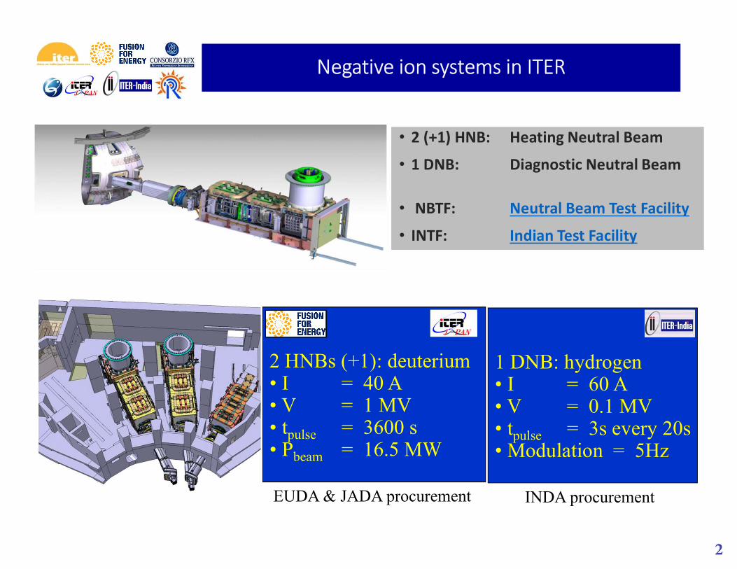
• 2 (+1) HNB: Heating Neutral Beam
• 1 DNB: Diagnostic Neutral Beam
• NBTF: Neutral Beam Test Facility
• INTF: Indian Test Facility
• 2 (+1) HNB: Heating Neutral Beam
• 1 DNB: Diagnostic Neutral Beam
• NBTF: Neutral Beam Test Facility
• INTF: Indian Test Facility
1 DNB: hydrogen • I = 60 A• V = 0.1 MV• tpulse = 3s every 20s• Modulation = 5Hz
INDA procurement
2 HNBs (+1): deuterium• I = 40 A• V = 1 MV• tpulse = 3600 s• Pbeam = 16.5 MW
EUDA & JADA procurement
Negative ion systems in ITER
2
3

Indian Test FacilityTransport Duct
Second Calorimeter
Cryopumps
Residual Ion Dump
Neutraliser
Ion source and accelerator100kV hushing
Calorimeter
HV transmission lineCooling water
system
Indian Test Facility (INTF)
Refer contribution number FIP P1-40 for R&D STATUS OF INDIAN TEST FACILITY FOR ITER DNB CHARACTERIZATION
FULL SCALE NEUTRAL BEAM TEST BEDLargest Beam line till date
4

Jaydeep Joshi et [email protected]
TECHNOLOGIES FOR REALIZATION OF LARGE SIZE RF SOURCES FOR –VE NEUTRAL BEAM SYSTEMS FOR ITER -Challenges, experience
and path ahead
FIP/1-3Rb
FIP/1-3Ra
PROGRESS IN ITER NEUTRAL BEAM FACILITY Toigo et al
DEMONSTRATION OF 1 MV VACUUM INSULATION FOR THE VACUUM INSULATED
BEAM SOURCE IN THE ITER NB SYSTEM
FIP/1-3Rc
Kojima et [email protected]
Presented by: Jaydeep Joshi on behalf of FIP/1-3Ra, FIP/1-3Rb and FIP/1-3Rc
27th IAEA-FEC, Gandhinagar, October 2018
5

© ITER-India, IPR (India)
RF Ion Source for –ve Neutral Beam system
Cross section of Beam Source
RF Based Ion Source with 8 RF drivers (1.5m x 1.9m x 1.1m)
Accelerator( 1.4m x 2.2m x 0.4m)
• Designed to produce a 100keV, 60A, 60MW Hydrogen beam• To measure the Helium ash content in the Deuterium–Tritium (D-T) phase of the
ITER machine using the Charge Exchange Recombination Spectroscopy (CXRS)
J. Joshi et al., 27th IAEA-FEC, Gandhinagar, October 2018 6
© ITER-India, IPR (India)
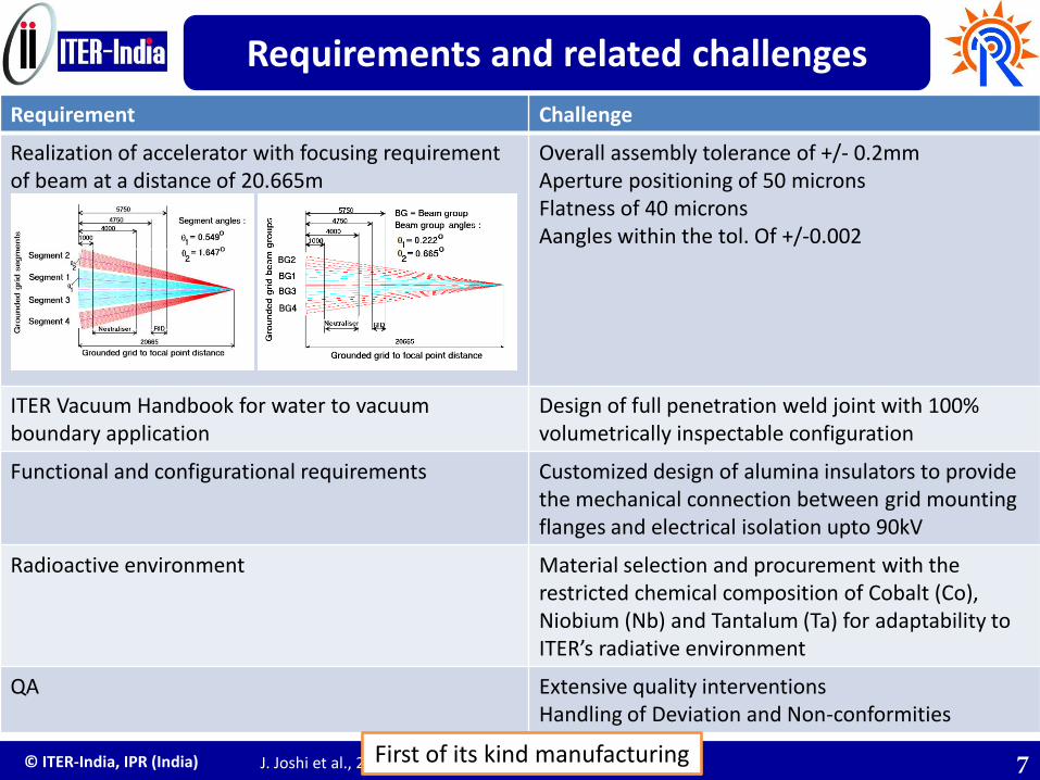
Requirements and related challenges
Requirement Challenge
Realization of accelerator with focusing requirement of beam at a distance of 20.665m
Overall assembly tolerance of +/- 0.2mmAperture positioning of 50 micronsFlatness of 40 micronsAangles within the tol. Of +/-0.002
ITER Vacuum Handbook for water to vacuum boundary application
Design of full penetration weld joint with 100% volumetrically inspectable configuration
Functional and configurational requirements Customized design of alumina insulators to provide the mechanical connection between grid mounting flanges and electrical isolation upto 90kV
Radioactive environment Material selection and procurement with the restricted chemical composition of Cobalt (Co), Niobium (Nb) and Tantalum (Ta) for adaptability to ITER’s radiative environment
QA Extensive quality interventionsHandling of Deviation and Non-conformities
J. Joshi et al., 27th IAEA-FEC, Gandhinagar, October 2018First of its kind manufacturing 7
© ITER-India, IPR (India)
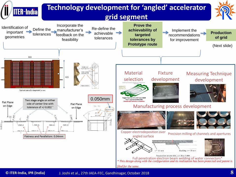
Technology development for ‘angled’ accelerator grid segment
Identification of
important
geometries
Define the
tolerances
Incorporate the
manufacturer’s
feedback on the
feasibility
Re-define the
achievable
tolerances
Prove the
achievability of
targeted
tolerances by
Prototype route
Implement the
recommendations
for improvement
Production
of grid
Material selection
Fixture development
Manufacturing process development
Measuring Technique development
Copper electrodeposition over angled surface
Precision milling of channels and apertures
Full penetration electron beam welding of water connectors** This design along with the configuration and its realization has been protected and patent is
filed for the same.
(Next slide)
J. Joshi et al., 27th IAEA-FEC, Gandhinagar, October 2018
0.050mm
8

© ITER-India, IPR (India)
Technology development for ‘angled’ accelerator grid segment
Production of grid
• Production with incorporating the
recommendations-> led to the best possible
methodology of manufacturing
• Three segments of Plasma Grid segments
have been produced till now.
• Effect of minor deviation on functionality is
assessed to move ahead for production
Beam group angles (Deg) Beam group plane flatness (microns) Aperture position (microns)
BG 1 BG 2 BG 3 BG 4 BG 1 BG 2 BG 3 BG 4 BG 1 BG 2 BG 3 BG 4
NominalValue 0.665 0.222 0.222 0.665 0 0
TargetedTolerance +/-0.002 +/-0.002 +/-
0.002+/-
0.002 40 50
Deviation-Segment 3 -0.003 0.010 -0.003 -0.011 197 136 86 116 21 23 25 38
PrototypeGrid -0.072 0.031 -0.014 -0.091 166 106 81 75 42 35 67 96
• Typical values of the achieved dimensions
J. Joshi et al., 27th IAEA-FEC, Gandhinagar, October 2018 9

© ITER-India, IPR (India)
Welding Technology development
Compatibility *with respect to IVH
* This design along with the configuration and its realization has been protected and patent is filed for the same.
Weldability* RepairabilityDissimilar
material welding
Full penetration CuOF to CuOF
EBW joint with 100% volumetric
examinable configuration
As welded seam
Full penetration EBW of
CuOF to Inconel joint
with strength in the
range of 234 to 261
MPa
Macro-picture of the
weld seam
• An important aspect of
production of grid
• Requires customized
solution for repair,
depending on the type of
defect and location of
defect
• Re-fuse the weld seam,
within the parameter
range Separate
qualification has been
performed to ensure the
strength as equivalent to
the original weld seam
(a) front side
(b) root side
RT image
of Weld seam
J. Joshi et al., 27th IAEA-FEC, Gandhinagar, October 2018 10

© ITER-India, IPR (India)
Post Insulator Manufacturing
J. Joshi et al., 27th IAEA-FEC, Gandhinagar, October 2018 11

© ITER-India, IPR (India)
Post Insulator Manufacturing
Broken at 16kN
Broken at 13kN
Spec requirement: 10kN
Prototyping: To establish (1) manufacturing route (2) to qualify them for mechanical and
electrical specification (3) to assess the feasibility of stringent tolerances on the assembly
Mechanical test Electrical test
Total 40 Nos. of Post insulators have been manufactured with end flange flatness
of 60 microns in assembled condition
J. Joshi et al., 27th IAEA-FEC, Gandhinagar, October 2018 12

© ITER-India, IPR (India)
Major components produced till now
Plasma Grid Segments-3 Nos.
Post Insulators-40 Nos.
Soft Iron Plate segment
Electron Dump Panels- 10 Nos.
EG Mounting Flange GG Flange
Rear Driver Plate
Plasma Box components and Faraday shield
Technologies involved: - High precision milling of
copper - Vacuum Brazing - Electron beam welding of
copper and dissimilar material
- Copper Electro deposition - Ceramic to metal joining - Heavy fabrication of
stainless steel - Deep hole drilling
J. Joshi et al., 27th IAEA-FEC, Gandhinagar, October 2018 13

© ITER-India, IPR (India)
Non-conformities and deviation
Extensive Quality interventions:
Tool to ensure and establish the close adherence of manufacturing activities with
respect to laid procedures
Each NC and DR to be supported by technical assessments (like FEA,
experimentations, prototyping, imposing additional inspection / test etc.) and check
that they do not impact the overall functionality of the system
J. Joshi et al., 27th IAEA-FEC, Gandhinagar, October 2018 14

© ITER-India, IPR (India)
• ‘angled’ grid segment manufacturing remains a challenge, even after establishing thecomplete manufacturing procedure through 1:1 prototype. Each segment has to behandled with careful monitoring at all the stages of production
• Welding for vacuum boundary connection according to ITER requirements, is one ofthe most critical activity in terms of process selection, configuration and itsqualification for timely execution of the project
• Inspite of sufficiently detailed and thoroughly detailed specification, there arepossibilities of deviations to suit the manufacturing needs, which have to beaccommodated without impact on the function of components
• Prototyping is essential for the components where no past experience is available toestablish the feasibility and to unfold the uncertain areas of manufacturing
• It is essential to be a ‘Technical Partner’ to ‘Contractor’ for every challenge they comeacross to fulfil the specification requirement, for the success of such a challengingproject.
• Significant learnings generated from this manufacturing is expected to provide theguideline on manufacturing design for upcoming ITER ion sources with similarchallenges for seamless manufacturing with reduced time and efforts.
Summary
J. Joshi et al., 27th IAEA-FEC, Gandhinagar, October 2018 15
Jaydeep Joshi et [email protected]
TECHNOLOGIES FOR REALIZATION OF LARGE SIZE RF SOURCES FOR –VE NEUTRAL BEAM
SYSTEMS FOR ITER -CHALLENGES, EXPERIENCE AND PATH AHEAD
FIP/1-3Rb
FIP/1-3Ra
PROGRESS IN ITER NEUTRAL BEAM FACILITY Toigo et al
DEMONSTRATION OF 1 MV VACUUM INSULATION FOR THE VACUUM INSULATED
BEAM SOURCE IN THE ITER NB SYSTEM
FIP/1-3Rc
Kojima et [email protected]
Presented by: Jaydeep Joshi on behalf of FIP/1-3Ra, FIP/1-3Rb and FIP/1-3Rc
27th IAEA-FEC, Gandhinagar, October 2018
16

SPIDER: full scale prototype of HNB/DNB source
Optimisation of production of negative ions
in terms of:
Density
Uniformity
Stability
Co-extracted electrons
3x Cs ovens
8x RF drivers
Extractor and accelerator
Toigo et al., 27th IAEA-FEC, Gandhinagar, October 2018 17

SPIDER Components
STRIKE
High resolution calorimeter
Vacuum-insulated beam source
Toigo et al., 27th IAEA-FEC, Gandhinagar, October 2018Beam Dump
Vacuum Vessel
Beam Source
18
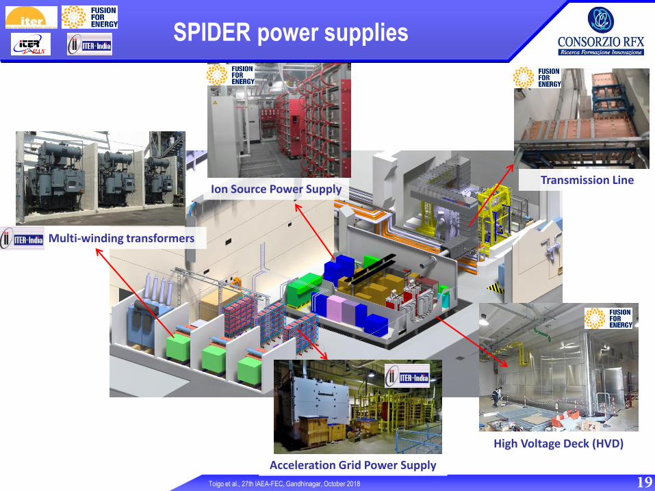
SPIDER power supplies
Acceleration Grid Power Supply
Multi-winding transformers
Toigo et al., 27th IAEA-FEC, Gandhinagar, October 2018
Transmission Line Ion Source Power Supply
High Voltage Deck (HVD)
19

SPIDER beam source installation
In March 2018
– all connections and vacuum vessel lid
closed
– leak test of hydraulic circuits from
external flanges started
Toigo et al., 27th IAEA-FEC, Gandhinagar, October 2018 20

First SPIDER operations
SPIDER operation started on 4 June 2018
After some tuning, first plasma ignition on 6 June 2018 with 1/4 source
Toigo et al., 27th IAEA-FEC, Gandhinagar, October 2018 21

Characterisation of source plasma
P1 P2
Toigo et al., 27th IAEA-FEC, Gandhinagar, October 2018
IPGF scan with different RF
powers (psource=0.24Pa; IISBI=0A)
IPGF scan with different psource
(RF power=25kW; IISBI=0A)
22

Source emission spectroscopy
in first SPIDER experiments
Hb radiation through drivers: RF power scan
Toigo et al., 27th IAEA-FEC, Gandhinagar, October 2018 23

MITICA full scale prototype of ITER HNB
HV Bushing
HV Transmission Line
Optimisation of neutral
beam in terms of:
Performances
Reliability
Availability
Unit H D
Beam energy keV 870 1000
Acceleration current A 46 40
Max Beam Source pressure Pa 0.3 0.3
Beamlet divergence mrad ≤7 ≤7
Beam on time s 3600 3600
Co-extracted electron fraction (e-/H
-) and (e
-/D
-) <0.5 <1
Toigo et al., 27th IAEA-FEC, Gandhinagar, October 2018 24

MITICA components
CRYOGENIC PUMPS
CALORIMETER RESIDUAL ION DUMP NEUTRALIZER
BEAM SOURCE
Toigo et al., 27th IAEA-FEC, Gandhinagar, October 2018
Procurement contracts of
mechanical components
are all in progress
Beam Source procurement is in the critical line. Procurement contract signed in 2018; delivery expected in 2022
25

MITICA power supply system
1MV
AGPS-DC
Generator
AGPS
Conversion system
60MW CW
HV Transmission Line
HV Bushing Vacuum Vessel
1MV Faraday Cage (hosting
Ion Source PSs)
Toigo et al., 27th IAEA-FEC, Gandhinagar, October 2018 26

AGPS-DCG insulating tests:
1.2MV (1h),1.06MV (5h)
1st STEP 1200kV-1 HOUR 2nd STEP 1060kV-5 HOURS
First HV insulating tests successfully passedToigo et al., 27th IAEA-FEC, Gandhinagar, October 2018 27

NBTF status
Toigo et al., 27th IAEA-FEC, Gandhinagar, October 2018
SPIDER
– Experimentation started in 2018
– Plants and diagnostics entering into operation one by one
– Characterisation of source and beam in progress
– Increase of parameters planned from 2019
MITICA
– High voltage power supplies almost completed and under test on-site
– Other auxiliary plant systems under installation and/or commissioning phase
– All procurement contracts for mechanical components in progress
– Expected delivery on site of Beam Source in 2022
28

Collaborations of NBTF
Toigo et al., 27th IAEA-FEC, Gandhinagar, October 2018 29
Jaydeep Joshi et [email protected]
TECHNOLOGIES FOR REALIZATION OF LARGE SIZE RF SOURCES FOR –VE NEUTRAL BEAM
SYSTEMS FOR ITER -CHALLENGES, EXPERIENCE AND PATH AHEAD
FIP/1-3Rb
FIP/1-3Ra
PROGRESS IN ITER NEUTRAL BEAM FACILITY Toigo et al
DEMONSTRATION OF 1 MV VACUUM INSULATION FOR THE VACUUM INSULATED
BEAM SOURCE IN THE ITER NB SYSTEM
FIP/1-3Rc
Kojima et [email protected]
Presented by: Jaydeep Joshi on behalf of FIP/1-3Ra, FIP/1-3Rb and FIP/1-3Rc
27th IAEA-FEC, Gandhinagar, October 2018
30

Demonstration of 1 MV vacuum insulation for the vacuum insulated beam source in the ITER NB system
FIP/1-3Rc
ITER NB system
1MV transmission line
1MV DCGenerators1MV transformer
HV Bushing
Beam Source Vessel
< Issue of 1 MV insulation for Beam Source >• Beam Source(BS) installed in vacuum (1 MV) directly faces to the
vessel (0 V), therefore 1 MV vacuum insulation with 0.9 m gap isrequired, which was originally designed by extrapolation fromsmall-scale experiments.
• Recent experiment indicated voltage holding with such long gapwas much lower than expected.
• JADA delivers 3 sets of 1 MV power supply and an 1 MV accelerator of beam source for ITER NB.• So far, insulation technology for DC 1 MV in gas, oil, water and air has been developed.
Vacuum insulation of ultra-high voltage of 1MV is the most critical issue.
31

Design basis of voltage holding capability on corner regionhas been developed for the first time.
FIP/1-3Rc
These empirical scaling for plane, coaxial and corner are easily applicable to the design of the ITER BS and HVB.
<Scaling for design of corner region>• EV value (Breakdown indicator) has
been investigated by using severalcylindrical configurations.
• Allowable ELV is found to be limitedaccording to surface area (~R)
→ Empirical scaling to design the electric field on corner.
<Recent experiment for 1 MV vacuum insulation>• Voltage holding capability of HVB was based on the empirical scaling for plane and coaxial electrodes.• Available voltage was limited to 0.7 MV due to breakdowns at 1.3 m single gap where
>1 MV was expected.→ Effect of locally concentrated electric field (EL) on corner was not fully understood
Coaxial electrodes
Corner
32

Voltage holding capability of vacuum insulated beam source has been analyzed by the empirical scaling.
FIP/1-3Rc
<Electric Field Analysis for BS and HVB >• Based on the empirical scaling, EV is analyzed for the BS and HVB in the vessel.
• Although the electric field E is not so high (< 3kV/mm) ,high voltages caused higher EV than allowable level.
• Estimated total voltage holding capability ~ 0.6 MV
→ E is almost saturated even in large R.
Possible measure is inserting shields having intermediate potentials to reduce applied V.
0.4 MV
0.6 MV
0.8 MV1 MV
0.2 MV
Higher V
33

Intermediate shields for the beam source has been developedas measure for the 1 MV vacuum insulation.
FIP/1-3Rc
• Required gap length between shields and electric filed at the corner has been designed.
• Estimated voltage has been improved from 0.6 MV to >1 MV.
<Design of shields for the BS and HVB in the vessel>• An intermediate shield can be simplified as plane, coaxial and corner regions.• Gap and electric field on corner is optimized to maximize the total voltage holding capability• Number of the shields has been analyzed.
34

1 MV vacuum insulation has been achieved by applying the developed intermediate shields for the HVB.
FIP/1-3Rc
The design basis of the 1 MV vacuum insulation with intermediate shieldshas been demonstrated.
This design technique is directly applicable to the BS for ITER too.
Voltage holding capability has been much improved from 0.7 to 1 MV.
<Demonstration of Improvement by Shields>• Intermediate shield for the HVB has been developed by taking into account the all scaling.• Voltage holding tests in vacuum were carried out by using the HVB with the shields.
35

SUMMARY
Successful demonstration of collaborative efforts in the area of technology developments, installation, operation and physics experiments towards the realization of ITER NB system
36

THANK YOU