an 189: simulating nios embedded processor...
TRANSCRIPT

February 2003, ver. 2.1 Application Note 189
Simulating Nios EmbeddedProcessor Designs
Introduction Simulation is an important part of the design process. Register transfer level (RTL) simulation verifies that a design performs as the designer intended, while gate-level simulation considers device-level timing to provide the most accurate simulation of how the completed design will operate in silicon.
When simulating an embedded processor, the system designer also uses RTL and gate-level simulation to find out exactly what is happening in the processor at any point in time. Traditionally, this simulation is called emulation. There are two types of emulators: software and hardware.
� Software—A software emulator contains a model of the processor’s operation. The model is loaded into a program that shows the instruction flow. The designer can then direct the emulator to run the code as the actual processor would and examine aspects of the operation, such as internal register values while the code is executing.
� Hardware—A hardware emulator performs a function similar to a software emulator, however, it uses an external hardware device to emulate the function of the target processor. Hardware emulators are commonly used during the development of full-custom processors.
System-on-a-programmable-chip (SOPC) designers have an additional tool for embedded development and debugging purposes: hardware description language (HDL) simulation tools such as the ModelSim simulator. ModelSim can perform RTL simulation using Verilog HDL or VHDL code or can perform timing simulation using the Standard Delay Format (SDF) Files (.sdf) and VHDL Output Files (.vho) or Verilog Output Files (.vo) generated by the Quartus® II software.
Nios® development kits include support for system-level simulation. This application note describes the simulation flow and process using an example Nios design and the ModelSim simulator, and should provide you with a better understanding of how to perform system-level simulation of embedded processor designs.
Altera Corporation 1
AN-189-2.1
AN 189: Simulating Nios Embedded Processor Designs
Before You Begin
The instructions in this document assume that you have a working knowledge of SOPC Builder, which you use to create Nios processor designs, and the ModelSim simulator. Additionally, you should have the following software installed:
� Quartus II version 2.2 or higher
� ModelSim PE, SE, EE, or ModelSim-Altera version 5.6a or higher
� Nios embedded processor version 3.0—Previous versions of the Nios processor support simulation, however, the instructions in this application note are for version 3.0.
Simulation Walkthrough
The following sections walk you through the simulation process for an example Nios design, including:
� “Simulation Settings” on page 2� “Getting Started in ModelSim” on page 10� “Analyzing the Simulation Results” on page 15
Simulation Settings
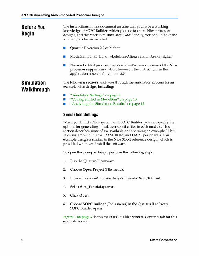
When you build a Nios system with SOPC Builder, you can specify the options for generating simulation-specific files in each module. This section describes some of the available options using an example 32-bit Nios system with internal RAM, ROM, and UART peripherals. This example design is similar to the Nios 32-bit reference design, which is provided when you install the software.
To open the example design, perform the following steps:
1. Run the Quartus II software.
2. Choose Open Project (File menu).
3. Browse to <installation directory>\tutorials\Sim_Tutorial.
4. Select Sim_Tutorial.quartus.
5. Click Open.
6. Choose SOPC Builder (Tools menu) in the Quartus II software. SOPC Builder opens.
Figure 1 on page 3 shows the SOPC Builder System Contents tab for this example system.
2 Altera Corporation
AN 189: Simulating Nios Embedded Processor Designs
f Refer to the SOPC Builder Data Sheet or Nios Hardware Development Tutorial for the Nios Development Board, Stratix Edition for more information on setting options in SOPC Builder.
Figure 1. Example 32-Bit Nios System
Memory Initialization
To display the code execution during simulation, the ModelSim software must be able to read the memory that contains the code. If you use the on-chip memory peripheral (RAM or ROM), SOPC Builder can create memory initialization files (.dat files) in your Nios simulation directory. These files contain code and data in Hexadecimal format. The ModelSim software automatically reads the files when it opens the HDL code that represents the on-chip memory that you are using.
1 SOPC Builder creates the Nios simulation directory, <Quartus II project directory>\<SOPC Builder system name>_sim, when you generate a Nios system.
To set up the on-chip memory peripheral to create a memory initialization file, perform the following steps in the System Contents tab of SOPC Builder:
1. Double-click the boot_rom memory peripheral. The On-chip Memory - boot_rom dialog box opens.
2. Click the Contents tab.
Altera Corporation 3
AN 189: Simulating Nios Embedded Processor Designs
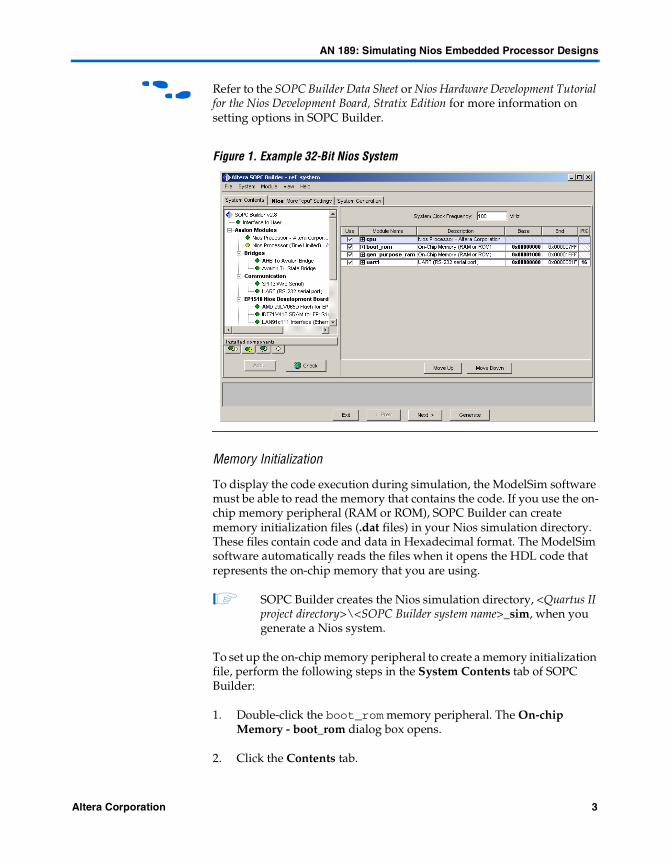
3. Select GERMS monitor. See Figure 2 on page 4.
Figure 2. Initializing Boot Monitor ROM with GERMS
1 In addition to the GERMS monitor, SOPC Builder has a variety of options for initializing memory. You can access these options in the Contents tab of the memory wizard.
- The Blank option initializes the memory with zeros.- The Build option initializes the memory with either the
output of a previously compiled source file—a Memory Initialization Format (.mif) or S-record (.srec) file—or by compiling a source file automatically using Assembly (.s) or C (.c) file(s).
- The File option allows you to initialize memory with the contents of any file.
- The Command option allows you to execute any command as you would in the Nios SDK Shell and use the results of that command to initialize memory.
- The String option initializes the memory with text that you type into the wizard.
4. Click Finish to save your settings.
1 If your design targets a Stratix device, you cannot pre-initialize the M-RAM blocks, which are used for larger on-chip memory blocks, with content. However, you can pre-initialize M4K and M512 blocks.
4 Altera Corporation
AN 189: Simulating Nios Embedded Processor Designs
The Nios embedded processor version 3.0 supports simulation of memory operations in off-chip memory. SOPC Builder’s SRAM and flash memory wizards have a Simulation tab that is similar to the on-chip memory Contents tab shown in Figure 2, however, the Simulation tab includes an option to bypass the creation of simulation files for your SRAM or flash peripheral.
1 The memory content choices on the Simulation tab do not directly affect the contents of the SRAM or flash memory when your design is operating in an actual system. Instead, the choices you make are used to create simulation files to model the operation of the SRAM or flash as if its contents were those specified in the wizard. The off-chip memory initialization .dat files created for simulation are identical to those used to simulate the operation of on-chip memory in the ModelSim software. The method you use to program the SRAM or flash memory on the Nios development board (i.e., using the nios-run command) remains unchanged.
When you generate a system that contains off-chip memory that you want to simulate, SOPC Builder also generates Verilog HDL or VHDL simulation models for the off-chip memory. Because timing specifications vary for each memory peripheral, these models are not intended to be cycle accurate. However, they let you easily simulate a system in which code or data is accessed from off-chip memory. To obtain cycle-accurate simulation results of off-chip memory, you must provide your own model; many memory manufacturers currently provide Verilog HDL or VHDL models of their memory devices for this purpose. Once you obtain a model, you can use it in place of the simple models that SOPC Builder generates.
f For more details about simulation of off-chip memory and using third-party memory models, refer to “Off-Chip Memory Simulation” on page 26.
UART Peripheral Simulation Settings
You can customize the UART peripheral specifically for simulation. For example, during high-speed system simulation (e.g., 100 MHz), UART simulation can be painstakingly slow because the UART transmits approximately 11,500 characters per second at 115,200 bps. At this baud rate, an 11-bit character (8 bits, 1 start-bit, 2 stop bits) takes greater than 9,500 clock cycles to simulate at 100 MHz. To speed functional simulation, you can run the UART with a small baud divisor, which allows the UART to run at half the system clock speed. In this mode, one bit is transmitted every two clock cycles, or roughly one character per 10 clock cycles.
Altera Corporation 5

AN 189: Simulating Nios Embedded Processor Designs
Additionally, you can customize the data stream transmitted to the UART, which is useful for simulating operation of an application that normally requires a user to type text that is sent to the Nios application (e.g., via the GERMS monitor).
You specify how data streams transmit to the UART in one of the following ways:
� Using the Simulated RXD-Input Character Stream dialog box� Using the optional Interactive windows in the ModelSim software
You can use the Simulated RXD-Input Character Stream dialog box to enter a static set of UART RXD data that is presented during simulation. Each character is sent to the UART when system CPU(s) read the UART, asserting its rx_char_ready signal. Specifying the data stream in this dialog box is useful for simulating systems with a constant set of UART stimulus that is not updated during simulation. During system generation, SOPC Builder converts the predefined text to ASCII-encoded Hexadecimal data and writes it to the <UART peripheral name>_input_data_stream.dat file in your Nios simulation directory.
The Interactive windows allow you to enter or view UART stimulus while the ModelSim software is running, in a similar manner as you would communicate to the Nios development board via the UART. The only difference is that input and output are handled by two separate terminal windows. A virtual terminal window displays a prompt where you can type UART stimulus. You can type UART stimulus even while the ModelSim software is running, allowing true interactive simulation. If you turn on the Create ModelSim Alias to open interactive stimulus window for this UART option in the UART Stimulation Settings dialog box (see Figure 3), SOPC Builder creates an alias to activate the stimulus window.
1 If you choose the interactive stimulus option, the Simulated RXD-Input Character Stream dialog box’s contents are not sent to the UART during simulation; only interactive stimulus is sent.
In addition to the interactive stimulus option, SOPC Builder can create a ModelSim alias to generate a streaming output UART window during simulation. When turned on, this option displays a window showing all UART TXD data. If you choose both interactive stimulus and streaming
6 Altera Corporation

AN 189: Simulating Nios Embedded Processor Designs
output simulation options, you can use both windows simultaneously during ModelSim simulation creating a virtual terminal display.
To set up the UART peripheral for simulation, perform the following steps in the System Contents tab of SOPC Builder:
1. Double-click the uart1 peripheral. The UART dialog box opens.
2. Click the Simulation tab.
3. Turn on the Create ModelSim Alias to open streaming output window for this UART option.
4. Turn on the Create ModelSim Alias to open interactive stimulus window for this UART option.
5. Indicate the transmitter baud rate. Select accelerated (use divisor = 2) to reduce the functional simulation time.
6. Click Finish when you are done.
Figure 3 shows example UART simulation settings.
Figure 3. UART Simulation Settings Dialog
Altera Corporation 7
AN 189: Simulating Nios Embedded Processor Designs
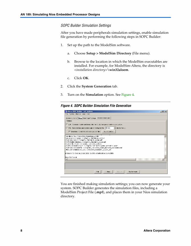
SOPC Builder Simulation Settings
After you have made peripherals simulation settings, enable simulation file generation by performing the following steps in SOPC Builder:
1. Set up the path to the ModelSim software.
a. Choose Setup > ModelSim Directory (File menu).
b. Browse to the location in which the ModelSim executables are installed. For example, for ModelSim-Altera, the directory is <installation directory>\win32aloem.
c. Click OK.
2. Click the System Generation tab.
3. Turn on the Simulation option. See Figure 4.
Figure 4. SOPC Builder Simulation File Generation
You are finished making simulation settings; you can now generate your system. SOPC Builder generates the simulation files, including a ModelSim Project File (.mpf), and places them in your Nios simulation directory.
8 Altera Corporation
AN 189: Simulating Nios Embedded Processor Designs
By default, the Run ModelSim button in the System Generation tab is enabled after your system has finished generating. Click Run ModelSim to run the ModelSim software automatically and load the project file generated for your system. This option only functions if you have specified the correct path to the ModelSim software using the Setup command (File menu).
1 If you do not set up the path to the ModelSim software in SOPC Builder, SOPC Builder issues a warning message at the end of system generation and generates all simulation files except the .mpf.
f Refer to the SOPC Builder Data Sheet and Nios Hardware Development Tutorial for the Nios Development Board, Stratix Edition for more information on generating your design.
Generated System Simulation Files
When system generation completes the Nios simulation directory contains all of the files necessary for simulation. Table 1 describes the files that are created.
Table 1. File Generated for Nios Simulation (Part 1 of 2)
File Extension Purpose
.mpf ModelSim project file. This file is created if SOPC Builder finds the ModelSim path. If you open this file in ModelSim, the directories and paths are set for simulation and the simulation macros described in Table 2 are initialized.
.do ModelSim macro execution scripts.
The setup_sim.do file initializes the macros listed in Table 2.
The wave_presets.do file generates a list of default signals that are displayed in the waveform window.
The virtuals.do file sets up a virtual signal that translates Nios operation codes (or opcodes) into instructions, allowing you to view assembly instructions (e.g., MOV, ADDI) during simulation.
Altera Corporation 9

AN 189: Simulating Nios Embedded Processor Designs
Getting Started in ModelSim
This section describes some basic steps to get you started running your simulation in the ModelSim software. For complete instructions on using the software, refer to the ModelSim Tutorial.
Perform the following steps to begin simulation using SOPC Builder-generated ModelSim Project File (.mpf) located in your Nios simulation directory.
1. Run the ModelSim software.
2. Unless you have turned it off previously, the Welcome to ModelSim <version> dialog box displays. Choose Open a Project.
If the welcome dialog box does not display, choose Open > Project (File menu).
3. Browse to the Nios simulation directory.
4. Select the ModelSim project file.
5. Click Open.
.dat Memory initialization files in Hexadecimal format. These files are used for simulation only. You can modify the file contents without altering the files used in synthesis or place-and-route. SOPC Builder creates .dat files for any on-chip memory peripheral(s) in your system. The files have a name that is similar to the peripheral name. For example, an on-chip ROM named Boot_ROM has an initialization file named Boot_ROM_lane0.dat. Memory peripherals that are byte-addressable have a .dat file for each addressable byte. These files have _lanex appended to the name, where x is a number. For example, a 32-bit ROM has four .dat files with _lane0 through _lane3.
To simulate an input character stream to the UART peripheral (as described in “UART Peripheral Simulation Settings” on page 5), SOPC Builder creates a separate .dat file with Hexadecimal data representing the input character stream.
Table 1. File Generated for Nios Simulation (Part 2 of 2)
File Extension Purpose
10 Altera Corporation

AN 189: Simulating Nios Embedded Processor Designs
6. Execute the setup_sim.do file (see Figure 5), which initializes the macros described in Table 2, by typing the following command at the ModelSim prompt:
do setup_sim.do r
These macros make it easy for you to load the design and recompile it after making code changes. To execute a macro, type the letter corresponding to the macro at the ModelSim prompt.
Figure 5. Running Initialization Script
Altera Corporation 11

AN 189: Simulating Nios Embedded Processor Designs
7. Execute the s macro to load the design.
8. Execute the w macro to display the ModelSim waveform window with example signals that were automatically generated for your system. These signals are separated by function and include signals useful for debugging. Figure 6 on page 13 shows the default waveform window for this walkthrough.
The example signals are a starting point for your analysis of the Nios system behavior. You can add or remove signals as described in “Adding & Removing Waveform Signals” on page 25. Table 3 on page 14 summarizes the types of signals displayed during simulation.
9. Execute the uart1_log macro to display the streaming output window for uart1.
10. Execute the uart1_drive macro to display the interactive stimulus window for uart1.
Table 2. Nios Simulation Macros
Macro Function
s Recompiles the Nios processor and peripheral source code and then reloads the design into the ModelSim work library for simulation. This macro resets the entire simulation.
c Recompiles all software source code and regenerates the software development kit (SDK) directory within your Nios project without altering your processors or peripherals. This option is useful during software development.
w Loads the wave_presets.do file, which contains predefined ModelSim waveform window information. The wave_presets.do file loads the common signals from all of the processors and peripherals that reside on-chip and displays the ModelSim waveform window.
l Sets up the ModelSim List window with predefined signals for viewing simulation results in a list format. The list format is text-based instead of graphical.
<UART name>_log Optional. For each UART in the system, this macro is created if you turned on the streaming simulation option before system generation. When you run this macro, it opens a new window, similar to a terminal screen, showing TXD data from the UART.
<UART name>_drive Optional. For each UART in the system, this macro is created if you turned on the interactive stimulus option before system generation. When you run this macro, it opens a new window, similar to a terminal window, where you can send virtual data to the UART RXD signal during simulation.
h Help. Displays the available macros and their function
12 Altera Corporation

AN 189: Simulating Nios Embedded Processor Designs
Figure 6. Default Waveforms
Altera Corporation 13

AN 189: Simulating Nios Embedded Processor Designs
Table 3. Signals Shown in Simulation Waveform (Part 1 of 2)
Signal Group Description
Instruction Master (1) Signals related to instruction fetching, decoding, and execution. The address group shows the address sent to the memory where instructions are fetched, while read data shows the data read from memory (typically opcodes).
read_data_opcode is a virtual signal that decodes the opcode to determine the instruction type. This signal is useful when comparing the processor’s execution to a compilation disassembly report.
The wait, read, data valid, and flush signals show additional information on the status of the processor as it executes code (e.g., the read signal is asserted while the instruction master actively fetches code from memory).
Data Master (1) Signals related to reading and writing data to and from memory and memory-mapped peripherals in the Nios system. The read and write data buses show incoming and outgoing data to/from the CPU. These signals cannot be tri-stated because they are signals inside of the Altera device.
The address, read, write, and byte enable signals, like those of the instruction master bus signals, operate according to the Avalon™ bus specification. The signals display all bus transactions that the Nios data master initiates to its Avalon slaves.
Interrupt Control (1) Displays the interrupt request (IRQ) and the IRQ number of the most recent request.
General Purpose RAM Peripheral (gen_purpose_RAM) (2)
Signals depicting the operation of the on-chip RAM. These signals are almost identical to those of the Nios data master, however, they include a chip select, which is a result of address decoding in the RAM peripheral.
UART1 Bus Interface (2) Signals displaying the UART bus interface. These signals are similar to those of the RAM peripheral, however, the read and write lines are omitted for clarity (you can add them back in manually).
UART1 Internals (2) Internal UART signals showing the UART transmit (TX) and receive (RX) data registers. The signals decode the 8-bit TX and RX registers to ASCII text so that you can view the characters in the simulation waveform. The TX ready and RX character ready signals are also shown.
14 Altera Corporation
AN 189: Simulating Nios Embedded Processor Designs
Notes:(1) These signals are generated and displayed for each Nios CPU. (2) These signal groups appear because the example design has ROM, RAM, and UART peripherals. Whenever you
add a Nios peripheral to your design, a corresponding set of simulation signals are generated and added to the default waveform. The signal groups have names that are similar to the peripheral name in SOPC Builder (e.g. gen_purpose_RAM). These signals reflect the I/O to/from each peripheral’s slave port. Therefore, the signals may not share the same value as the corresponding signals in the Nios instruction/data master port unless a valid bus transaction has been initiated between the Nios processor and a specific peripheral.
(3) SDRAM controller signals are added to your waveform automatically if you use the Altera Avalon SDRAM Controller in your design. Because the simulation design files referenced in this application note do not use the SDRAM controller, you will not see SDRAM signals during the simulation walkthrough.
You have completed the basic simulation setup steps. You can use the ModelSim software to perform simulation as you would for any other Altera design.
Analyzing the Simulation Results
After you have loaded the design, you can simulate and analyze the operation of your Nios CPU(s), peripherals, and source code. You can start simulation using the commands in the Run menu or by executing the run command at the ModelSim prompt (e.g., use run 100 µs to run the simulation through 100 microseconds of time). The software supports standard time units such as ns, µs, and ms.
Boot ROM (boot_rom) (2) Read address and data out signals for the on-chip ROM peripheral.
SDRAM Controller (3) Signals showing the interface between the Avalon bus module and the SDRAM controller, SDRAM controller and SDRAM device(s), and signals internal to the SDRAM controller logic.
Signals from Avalon bus module to the SDRAM controller have the prefix az_, e.g., az_addr for the address bus input.
Signals from the SDRAM controller to the Avalon bus module have the prefix za_, e.g., za_data for data from the controller to Avalon bus module.
Signals between the SDRAM controller and external SDRAM device(s) have the prefix zs_, e.g., zs_ras_n for the row address strobe signal.
Signals internal to the SDRAM controller logic include the system clock (clk) and the current operation that the SDRAM controller is performing (CODE).
Table 3. Signals Shown in Simulation Waveform (Part 2 of 2)
Signal Group Description
Altera Corporation 15

AN 189: Simulating Nios Embedded Processor Designs
This section provides two analysis examples:
� The GERMS monitor interacting with a UART peripheral� A simple C program that exercises a parallel I/O (PIO) peripheral
GERMS Monitor Interacting with UART
This example analyzes the GERMS monitor executing in the Nios CPU and its interaction with the on-chip UART peripheral, including the interaction between the CPU and UART while exchanging character strings. The UART receives the character stream as defined in the interactive UART stimulus window, activated with the uart1_drive macro. The signal rx_data, which represents the UART’s 8-bit receiver register, displays the ASCII-encoded data received from the character stream.
Perform the following steps to provide stimulus to the UART and run the simulation:
1. Type m1000:4D6F6E6B into the UART interactive stimulus window (see Figure 7). This command directs the GERMS monitor, after boot-up, to write 0x4D6F6E6B to address 0x1000.
1 You can enter new commands into the interactive stimulus window when the + character is displayed. Running simulation either for a brief period of time until the preceding character string is received, or simply running continuously, allows you to enter more stimulus.
Figure 7. UART Character Streams
2. Run the ModelSim software by typing run 30µs to simulate for 30 microseconds.
16 Altera Corporation

AN 189: Simulating Nios Embedded Processor Designs
1 After 30 µs, you should see the system boot message and command from step 1 shown both in the ModelSim message window and the streaming UART output window.
3. Type a second GERMS command, m1004:00006579, in the interactive stimulus window.
4. Run the ModelSim software again by typing run 30µs to simulate for 30 microseconds. If you prefer, you may run for a longer period of time and let the simulator run continuously.
5. Enter a final command, m1000, to dump memory contents at address 0x1000. This step causes the UART to print out a hexadecimal memory dump from address 0x1000 to 0x103F.
6. Run the ModelSim software for another 120 µs to complete the memory printout over UART.
You can now analyze the entire system in operation, including GERMS monitor code execution, UART operation, system memory, and operation of the Avalon bus module.
Figure 8 shows a portion of the simulation for the example system described in “Simulation Settings” on page 2. Between 10 and 11µs, the waveform displays the m character from the input m1000:4D6F6E6B. As the GERMS monitor reads the receiver register from the UART, the remaining characters are transmitted to form the entire input string. As the UART receives each character, the rx_char_ready signal is asserted. The pipe characters (|) at the end of the waveform are the carriage return and linefeed characters.
Figure 8. UART Character Reception
Altera Corporation 17

AN 189: Simulating Nios Embedded Processor Designs
After the Nios CPU receives the m character, the UART receives additional characters. Figure 9 shows this operation in detail. At the solid vertical time bar, the GERMS monitor source code reads the UART’s receive register (shown as the data master d_read signal being asserted while the uart1 bus interface chipselect signal is asserted, indicating a read cycle to the UART). At this time, the readdata registers for the Nios data master and UART bus interface are set to 0x006D, which is the ASCII code for the m character.
1 During simulation, the rx_data signal shows 0 for the value 000 (from m1000). Although the rx_data signal displays only 0, the rx_char_ready signals is read three times, indicating that three 0 characters were read from the receive data line.
Figure 9. UART Receiving Additional Characters
As the ModelSim software continues to run, the Nios CPU executes all three GERMS commands. Following the last command (m1000), the GERMS monitor prints a memory dump, which includes the memory write operations performed in the first two GERMS commands. This display, shown in Figure 10, is shown both in the ModelSim command window as well as the UART’s streaming simulation output window.
18 Altera Corporation

AN 189: Simulating Nios Embedded Processor Designs
Figure 10. GERMS Monitor Memory Dump
+m1000:4d6f6e6b
+m1004:00006579
+m1000
#1000: 6E6B 4D6F 6579 0000 0000 0000 0000 0000#1010: 0000 0000 0000 0000 0000 0000 0000 0000#1020: 0000 0000 0000 0000 0000 0000 0000 0000#1030: 0000 0000 0000 0000 0000 0000 0000 0000+
C Code Exercising PIO Peripheral
This example demonstrates the correlation between the source code and the simulation output in a Nios system and analyzes the source code, disassembly, opcodes (machine code), and simulation results for the Nios CPU. This 32-bit example design contains:
� An on-chip ROM at address 0x0� An on-chip RAM at address 0x1000� A 32-bit PIO peripheral at address 0x2000, configured for output
only
f This C design, exercising a PIO peripheral, is located in the c:\altera\excalibur\sopc_builder_2_5\tutorials\sim_tutorial2 directory.
Unlike the previous example, this design does not run the GERMS monitor and does not use a UART for communication. Instead, the ROM is initialized with the port.c file shown in Figure 11.
Altera Corporation 19

AN 189: Simulating Nios Embedded Processor Designs
Figure 11. port.c Source Code Initialzing RAM
/* Filename: port.c* Example code for Nios simulation.* This program performs a continuous loop in which* an integer is incremented and then written to a* 32-bit PIO port at address 0x2000* (c) 2001 Altera Corporation*/
# define mypio *((int *)(0x2000))void main(void){
int i = 0;while(1){
i++;mypio = i;
}}
1 When accessing a PIO peripheral you typically use a pointer to an np_pio structure that is defined in the nios_peripherals.h file. For simplicity, this example defines a pointer, mypio, to the absolute memory location of 0x2000 so that writes to this memory location are sent to the PIO peripheral.
The port.c program infinitely loops while writing a steadily incrementing value to the 32-bit PIO port. Because the boot ROM is initialized with port.c, SOPC Builder automatically calls the nios-build command. When nios-build is executed, it generates several files and the main S-record (.srec) output file. The object dump (.objdump) file is useful for simulation because it shows the Assembly code that was generated by the assembler and the opcodes representing each assembly instruction in line with the original C code.
20 Altera Corporation

AN 189: Simulating Nios Embedded Processor Designs
Figure 12 is an excerpt from the port.objdump file that was generated for port.c:.
Figure 12. Excerpt of port.objdump
port.out: file format elf32-nios
Disassembly of section .text:
00000000 <nr_jumptostart>:0: 00 98 pfx %hi(0x0)2: 40 36 movi %g0,0x124: 00 98 pfx %hi(0x0)6: 00 6c movhi %g0,0x08: c0 7f jmp %g0a: 00 30 nopc: 4e 69 ext16d %sp,%o2e: 6f 73 usr0 %o7,%i3
00000010 <main>:
# define mypio *((int *)(0x2000))void main(void){
10: 17 78 save %sp,0x17int i = 0;
12: 01 34 movi %g1,0x0while(1)
14: b0 49 bgen %l0,0xd{
i++;16: 21 04 inc %g1
mypio = i;18: 01 a0 stp [%l0,0x0],%g1
}1a: fe 87 br 18 <main+0x8>1c: 21 04 inc %g1
}1e: df 7f ret20: a0 7d restore...
Altera Corporation 21

AN 189: Simulating Nios Embedded Processor Designs
The object dump listing shows several items on each line:
� A memory address (e.g., 1c:) � The opcodes (data stored in the boot ROM) at that memory location
(e.g., 21 04)� Assembly code corresponding to these opcodes (e.g., inc %g1)
The object dump file contains additional code such as startup routines, interrupt initialization, and other code that was brought in during the linking stage of compilation. In the object dump excerpt, addresses 0x0 through 0xE define the nr_jumptostart routine, which was linked after compilation. This routine calls the _start routine that appears later in the object dump listing (not shown).
Using the object dump listing you can view the correlation between the object dump file and execution in the Nios processor. In Figure 13, the beginning of the code execution is shown.
Figure 13. Start of Code Execution
The code executes upon initialization of an Altera device because all registers are cleared automatically on startup. Alternatively, asserting the Nios reset_n input causes the processor to restart. At the beginning of simulation in Figure 13, the Nios instruction master address is set to 0x0, and a read is performed soon after at that address.
22 Altera Corporation

AN 189: Simulating Nios Embedded Processor Designs
If you refer to the first few lines of the object dump listing, you can view the instructions that are fetched from memory:
00000000 <nr_jumptostart>:0: 00 98 pfx %hi(0x0)2: 40 36 movi %g0,0x12
The Nios CPU is little endian, but object dump listings are big endian. While at address 0x0, the Nios instruction master i_read_data signal is set to 9800, which correlates to 00 98 in the object dump file. The object dump shows that 00 98 is the opcode for a prefix instruction pfx %hi(0x0). In the waveform, the instruction master i_readdata_opcode automatically decodes 00 98 to indicate a prefix instruction.
1 The Nios CPU architecture is pipe lined. Therefore, the instruction that is fetched from memory is not the same as the one that is executed. The instruction_opcodes signal in the waveform represents the instruction that is executed, while the i_readdata_opcode shows the last opcode fetched from memory.
After instruction execution starts, you can observe the i_address incrementing as each new instruction is fetched. As the code execution shown in Figure 13 continues, the nr_jumptostart routine completes when the jump (jmp) instruction from ROM address 0x8 is executed. Then, the read data address changes to 0x26 where the _start routine begins. The _start routine then executes before returning control to the port.c program beginning at address 0x10.
Figure 14 shows the waveform after the code execution has advanced to the point where the main routine is entered at address 0x10 and the PIO output begins to change. The vertical time bar shows the location in which the instruction fetch address is 0x10, i.e., the beginning of the main routine as shown in the object dump (the in-line C code is removed for clarity.):
10: 17 78 save %sp,0x1712: 01 34 movi %g1,0x014: b0 49 bgen %l0,0xd16: 21 04 inc %g118: 01 a0 stp [%l0,0x0],%g11a: fe 87 br 18 <main+0x8>
Altera Corporation 23

AN 189: Simulating Nios Embedded Processor Designs
Next, the movi, bgen, inc, and stp instructions are fetched as shown by i_readdata_opcode. There is an initial delay following the branch to the main routine while the CPU pipeline is filled, resulting in a latency of three instructions before movi, bgen, inc, and stp appear in the instruction_opcode signal. Once the loop is established, the pipeline remains filled and there is no additional latency.
1 The increment (inc) instruction is actually shown as an add immediate (addi) instruction during simulation. It is shown as addi because increment is a pseudo instruction that, while generated during compilation and presented in the object dump, is later assembled to match the Nios instruction set.
As the stp instruction—which stores 32-bit data to memory—is executed, the CPU performs a write to the PIO peripheral near the dotted vertical time bar. At the same time, the data master’s d_write and d_address signals request a write to address 0x2000. The data written, 0x1, then appears on the PIO port outputs at the bottom of the waveform.
Figure 14. Start of PIO Write Loop
Figure 15 shows the PIO write loop once it has been established. Subsequent execution of the loop requires only three instructions—addi, stp, and br—to increment the value being written to the PIO, perform the write, and branch to the beginning of the loop again, respectively.
24 Altera Corporation

AN 189: Simulating Nios Embedded Processor Designs
Figure 15. PIO Write Loop Established
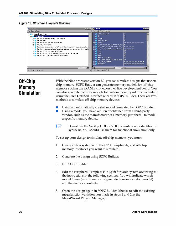
Adding & Removing Waveform Signals
To add or remove signals, use the Structure and Signals windows (View menu), which hierarchically divide your design for easy reference. The Structure window displays individual entities in your design and any sub-entities that they call. The Signals window shows the signals available for simulation. Figure 16 shows the Structure and Signals windows.
The Structure window shows the top-level Nios system module (the Nios CPU and internal peripherals). Each item in the Structure window corresponds to a design sub-entity. For example, the UART peripheral is listed as the_uart1:uart1. Click the sub-entity name to display its signals in the Signals window.
You can drag and drop signals from the Signals window to the waveform window to add them to the waveform. After you add a signal, you can edit it to display a different alias, radix (for buses), etc. Refer to the ModelSim documentation for instructions on making these settings.
You can delete a signal or group of signals from the waveform by selecting the signals(s) and then choosing Delete (Edit menu).
Altera Corporation 25
AN 189: Simulating Nios Embedded Processor Designs
Figure 16. Structure & Signals Windows
Off-Chip Memory Simulation
With the Nios processor version 3.0, you can simulate designs that use off-chip memory. SOPC Builder can generate memory models for off-chip memory such as the SRAM included on the Nios development board. You can also generate memory models for custom memory interfaces created using the User-Defined Interface wizard in SOPC Builder. There are two methods to simulate off-chip memory devices:
� Using an automatically created model generated by SOPC Builder.� Using a model you have written or obtained from a third-party
vendor, such as the manufacturer of a memory peripheral, to model a specific memory device.
1 Do not use the Verilog HDL or VHDL simulation model files for synthesis. You should use them for functional simulation only.
To set up your design to simulate off-chip memory, you must:
1. Create a Nios system with the CPU, peripherals, and off-chip memory interfaces you want to simulate.
2. Generate the design using SOPC Builder.
3. Exit SOPC Builder.
4. Edit the Peripheral Template File (.ptf) for your system according to the instructions in the following sections. You will indicate which model to use (an automatically generated one or a custom model) and the memory contents.
5. Open the design again in SOPC Builder (choose to edit the existing megafunction variation you made in steps 1 and 2 in the MegaWizard Plug-In Manager).
26 Altera Corporation

AN 189: Simulating Nios Embedded Processor Designs
6. Generate the design a second time to create the appropriate simulation files.
1 Before simulating off-chip memory other than the flash or SRAM provided on the Nios development board (as described in “Simulation Walkthrough” on page 2), you should be familiar with the PTF file, which defines a system created with SOPC Builder. Refer to the SOPC Builder Data Sheet for an overview of the PTF file.
Using Automatically Generated Memory Models
You can edit your system’s PTF file so that SOPC Builder automatically generates simple simulation models to simulate off-chip memory other than the flash or SRAM included on the Nios development board. These automatically generated models initialize with the memory contents defined in the CONTENTS section of the PTF file. If you want to specify a custom model, refer to “Specifying a Custom Model” on page 28.
To use a simple model, perform the following steps:
1. Open the PTF file in a text editor.
2. Add a Make_Memory_Model line within the SYSTEM_BUILDER_INFO section of the module for the off-chip memory device you want to simulate. The following example excerpt is from the MODULE section of a user-defined memory interface peripheral (the line in blue text is the added line):
SYSTEM_BUILDER_INFO{
Instantiate_In_System_Module = "1";Is_Enabled = "1";Date_Modified = "--unknown--";Make_Memory_Model = "1";
}
1 The SYSTEM_BUILDER_INFO section must be part of the peripheral’s MODULE section not the SLAVE section. Some peripherals have SYSTEM_BUILDER_INFO sections in both MODULE and SLAVE sections.
3. Populate the memory model with data as described in “Defining Memory Model Contents” on page 29.
4. Save the PTF file.
Altera Corporation 27

AN 189: Simulating Nios Embedded Processor Designs
When you generate your system, SOPC Builder creates a simulation comdel that is instantiated in the top level of your system. The instantiation is hidden from synthesis so that only the simulation software instantiates the model.
Specifying a Custom Model
Instead of generating a simple simulation model, you can specify a custom memory model. For example, you would specify a custom memory model if you have obtained a model from a memory manufacturer that describes the timing constraints of a specific device.
To use a custom model, perform the following steps:
1. Open the PTF file in a text editor.
2. Create a Verilog_Sim_Model_Files (for Verilog HDL users) or Vhdl_Sim_Model_Files (for VHDL users) line in the HDL_INFO section of your peripheral’s MODULE section. If the model has multiple HDL files, separate them using commas. The following example illustrates a Verilog HDL model with filename my_model.v:
HDL_INFO{
Verilog_Sim_Model_Files = "my_model.v";}
1 The file(s) specified are referenced for simulation with respect to the Nios simulation directory in your main project directory. If you place simulation model files in this directory, no special considerations for file/directory paths are needed. However, if your models reside in some other directory, you will need to specify a complete path for ModelSim.
3. To initialize the custom memory model to a specific value, perform the steps described in “Defining Memory Model Contents” on page 29.
4. Save the PTF file.
When you generate your system, SOPC Builder creates a simulation comdel that is instantiated in the top level of your system. The instantiation is hidden from synthesis so that only the simulation software instantiates the model.
28 Altera Corporation

AN 189: Simulating Nios Embedded Processor Designs
Defining Memory Model Contents
You define the contents of your off-chip memory peripheral by creating a CONTENTS section within the WIZARD_SCRIPT_ARGUMENTS section of your peripheral module. This information directs SOPC Builder to generate simulation .dat files that define the contents of your off-chip memory peripheral. The CONTENTS "Kind=" field directs SOPC Builder to initialize your off-chip memory model as blank (all zeros), with the GERMS monitor, with a file, etc. The following excerpt illustrates the settings to use an S-record file (my_contents.srec) to initialize a simulation model:
CONTENTS srec{
Kind = "build";Build_Info = "my_contents.srec";Command_Info = "";Textfile_Info = "";String_Info = "";
}
1 The CONTENTS section in your PTF file is identical to that created by SOPC Builder for simulating off-chip SRAM or flash peripherals. One method of ensuring that you create a properly formatted CONTENTS section is to temporarily direct SOPC Builder SRAM or flash wizard to generate contents using your specifications. You can copy the resulting CONTENTS section to the WIZARD_SCRIPT_ARGUMENTS of your user-defined peripheral module.
Conclusion Design verification is one of the most critical portions of any design cycle. With the SOPC design using the Nios embedded processor, you now have the ability to probe signals within the Nios CPU, its peripherals, and bus architecture simultaneously for system-level verification.
References For more information, refer to the following sources:
� Nios Hardware Development Tutorial for the Nios Development Board, Stratix Edition
� ModelSim Start Here Guide� ModelSim Tutorial
Documentation Feedback
Altera values your feedback. If you would like to provide feedback on this document—e.g., clarification requests, inaccuracies, or inconsistencies—send e-mail to [email protected].
Altera Corporation 29

AN 189: Simulating Nios Embedded Processor Designs
30 Altera Corporation
101 Innovation DriveSan Jose, CA 95134(408) 544-7000http://www.altera.comApplications Hotline:(800) 800-EPLDLiterature Services:[email protected]
Copyright 2003 Altera Corporation. Altera, The Programmable Solutions Company, the stylized Altera logo,specific device designations, and all other words and logos that are identified as trademarks and/or servicemarks are, unless noted otherwise, the trademarks and service marks of Altera Corporation in the U.S. andother countries. All other product or service names are the property of their respective holders. Altera productsare protected under numerous U.S. and foreign patents and pending applications, maskwork rights, andcopyrights. Altera warrants performance of its semiconductor products to currentspecifications in accordance with Altera’s standard warranty, but reserves the right tomake changes to any products and services at any time without notice. Altera assumes noresponsibility or liability arising out of the application or use of any information, product,or service described herein except as expressly agreed to in writing by Altera Corporation.Altera customers are advised to obtain the latest version of device specifications beforerelying on any published information and before placing orders for products or services.All rights reserved.