an 8ma, 3.8db nf, 40db gain cmos front-end for gps ...papers/compendium94-03/papers/2000/...tuning,...
TRANSCRIPT

279
An 8mA, 3.8dB NF, 40dB Gain CMOS Front-End for GPS Applications
F. Svelto S. Deantoni, G. Montagna R. Castello Dipartimento di Ingegneria “Studio di Microelettronica” Dipartimento di Elettronica Università di Bergamo, STMicroeletronics Università di Pavia Via Marconi5, I24044 Dalmine (BG) Via Ferrata 1, I27100 Pavia Via Ferrata 1, I27100 Pavia 039 035277311 039-0382505604 039-0382505213 [email protected] [email protected] [email protected] ABSTRACT
A fully differential 0.35µm CMOS LNA plus mixer, tailored to a double conversion architecture, for GPS applications has been realized. The LNA makes use of an inductively degenerated input stage and a resonant LC load, featuring 12% frequency tuning, accomplished by an MOS varactor. The mixer is a Gilbert cell like, in which an NMOS and a PMOS differential pair, shunted together, realize the input stage. This topology allows to save power, for given mixer gain and linearity. The front-end measured performances are: 40dB gain, 3.8dB NF, -25.5dBm IIP3, 1.3GHz input frequency, 140MHz output frequency, with 8mA from a 2.8V voltage supply.
Keywords
CMOS, low-power dissipation, design, communication, circuit-analog, low-power design, performances trade-off.
1. INTRODUCTION
RF building blocks, and complete receivers, realized in CMOS, and showing performance compatible with the most stringent standards have been proven [1-2]. Recently, the effort of researchers is devoted to increase the level of integration of these solutions. This means, for example, trying to achieve the specifications while minimizing the number of external components [3]. Moreover, though not mandatory, CMOS solutions, targeting single chip transceivers, should be differential. This is to insure an adequate rejection of the noise and interfering signals travelling through the common substrate. In this paper, we propose a fully differential 0.35µm LNA plus mixer, employing no external components and targeting the GPS standard. Experimental results show the following performances: 3.8dB noise figure, -25.5dBm IIP3, 40dB voltage gain, while drawing 8mA. Another 2mA are used by off-chip drivers, which however would not be required in a fully integrated receiver.
This solution is intended for a double conversion architecture with an IF of about 140MHz (i.e. about 10% of the carrier frequency). This means that the mixer translates the carrier frequency from RF to 140MHz. The narrowband LNA uses an inductively degenerated input stage and an LC load. The latter is electronically tunable via a MOS varactor shunting the fixed LC elements. The varactor is intended to compensate the spread in the IC passive components, due to process variations. The mixer follows the LNA, directly on-chip, and is based on a Gilbert cell. The voltage supply, in this design, is set to 2.8V. At 2.5V, the gain and the IIP3 do not change, whereas the noise figure raises to 4dB. 2. LNA DESIGN
The requirements set on the LNA input stage are: source impedance matching, minimum noise contribution, maximum transconductance gain. Furthermore, the IIP3 of the LNA should be maximized. It has been shown that the input stage which allows to achieve minimum noise figure, matched input impedance and maximum transconductance gain is the inductively degenerated NMOS one, shown in Figure 1, in its differential form [4]. In fact, this topology allows to achieve a real input impedance (given by ωT times LS, where ωT is the NMOS cutoff frequency) at the carrier frequency ωc (provided ωc =1/√(LS+LG)CGS, where CGS is the gate to source capacitance of the active devices). Due to the narrowband nature of telecommunication signals, it is desirable to have a narrowband RF signal processing, to get rid of out-of-band blockers.
Fig. 1: LNA input stage
M1 M2 LG
C C
Ipol
Ls Ls
RFP
LG
RFm
Permission to make digital or hard copies of all or part of this work for personal or classroom use is granted without fee provided that copies are not made or distributed for profit or commercial advantage and that copies bear this notice and the full citation on the first page. To copy otherwise, or republish, to post on servers or to redistribute to lists, requires prior specific permission and/or a fee. ISLPED ’00, Rapallo, Italy. Copyright 2000 ACM 1-58113-190-9/00/0007…$5.00.
280
This input stage is intrinsically narrowband, for the following reasons:
1. The input impedance is matched to the source impedance only at the carrier frequency. This means that the power transfer from the antenna to the receiver is maximum only at the carrier frequency.
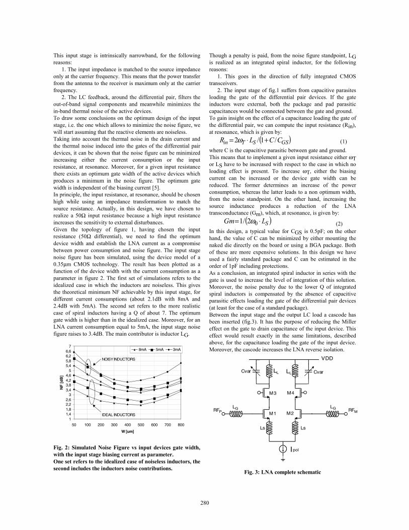
2. The LC feedback, around the differential pair, filters the out-of-band signal components and meanwhile minimizes the in-band thermal noise of the active devices. To draw some conclusions on the optimum design of the input stage, i.e. the one which allows to minimize the noise figure, we will start assuming that the reactive elements are noiseless. Taking into account the thermal noise in the drain current and the thermal noise induced into the gates of the differential pair devices, it can be shown that the noise figure can be minimized increasing either the current consumption or the input resistance, at resonance. Moreover, for a given input resistance there exists an optimum gate width of the active devices which produces a minimum in the noise figure. The optimum gate width is independent of the biasing current [5]. In principle, the input resistance, at resonance, should be chosen high while using an impedance transformation to match the source resistance. Actually, in this design, we have chosen to realize a 50Ω input resistance because a high input resistance increases the sensitivity to external disturbances. Given the topology of figure 1, having chosen the input resistance (50Ω differential), we need to find the optimum device width and establish the LNA current as a compromise between power consumption and noise figure. The input stage noise figure has been simulated, using the device model of a 0.35µm CMOS technology. The result has been plotted as a function of the device width with the current consumption as a parameter in figure 2. The first set of simulations refers to the idealized case in which the inductors are noiseless. This gives the theoretical minimum NF achievable by this input stage, for different current consumptions (about 2.1dB with 8mA and 2.4dB with 5mA). The second set refers to the more realistic case of spiral inductors having a Q of about 7. The optimum gate width is higher than in the idealized case. Moreover, for an LNA current consumption equal to 5mA, the input stage noise figure raises to 3.4dB. The main contributor is inductor LG.
Fig. 2: Simulated Noise Figure vs input devices gate width, with the input stage biasing current as parameter. One set refers to the idealized case of noiseless inductors, the second includes the inductors noise contributions.
Though a penalty is paid, from the noise figure standpoint, LG is realized as an integrated spiral inductor, for the following reasons:
1. This goes in the direction of fully integrated CMOS transceivers.
2. The input stage of fig.1 suffers from capacitive parasites loading the gate of the differential pair devices. If the gate inductors were external, both the package and pad parasitic capacitances would be connected between the gate and ground. To gain insight on the effect of a capacitance loading the gate of the differential pair, we can compute the input resistance (Rin), at resonance, which is given by:
( )GSSTin CCLR /1/2 +⋅= ω (1) where C is the capacitive parasitic between gate and ground. This means that to implement a given input resistance either ωT or LS have to be increased with respect to the case in which no loading effect is present. To increase ωT, either the biasing current can be increased or the device gate width can be reduced. The former determines an increase of the power consumption, whereas the latter leads to a non optimum width, from the noise standpoint. On the other hand, increasing the source inductance produces a reduction of the LNA transconductance (Gm), which, at resonance, is given by:
( )SLGm ⋅= 02/1 ω (2) In this design, a typical value for CGS is 0.5pF; on the other hand, the value of C can be minimized by either mounting the naked die directly on the board or using a BGA package. Both of these are more expensive solutions. In this design we have used a fairly standard package and C can be estimated in the order of 1pF including protections. As a conclusion, an integrated spiral inductor in series with the gate is used to increase the level of integration of this solution. Moreover, the noise penalty due to the lower Q of integrated spiral inductors is compensated by the absence of capacitive parasitic effects loading the gate of the differential pair devices (at least for the case of a standard package). Between the input stage and the output LC load a cascode has been inserted (fig.3). It has the purpose of reducing the Miller effect on the gate to drain capacitance of the input device. This effect would result exactly in the same limitations, described above, for the capacitance loading the gate of the input device. Moreover, the cascode increases the LNA reverse isolation.
Fig. 3: LNA complete schematic
M1 M2 LG LG
Ipol
Ls Ls
LL Cvar Cvar
VDD
RFP RFM
M3 M4
LL
11,41,82,22,6
33,43,84,24,6
55,45,86,26,6
7
50 100 200 300 400 500 600 700 800
W [um]
NF
[d
B]
8mA 5mA 3mA
IDEAL INDUCTORS
NOISY INDUCTORS
281
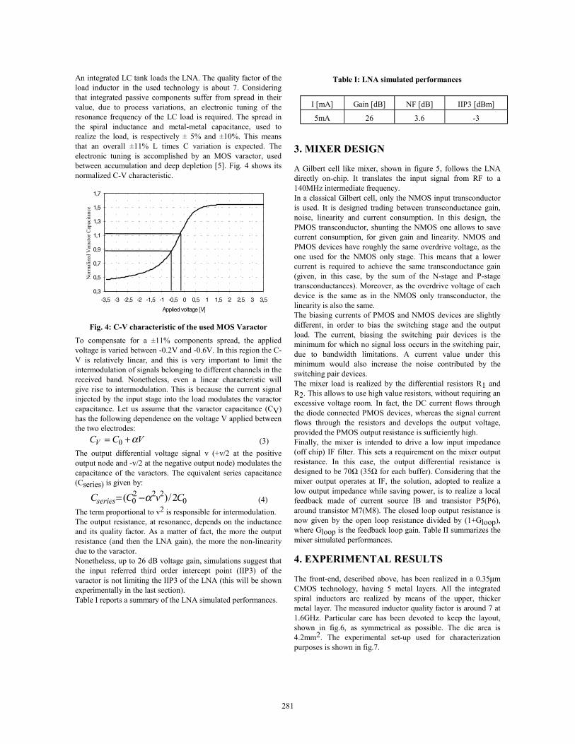
An integrated LC tank loads the LNA. The quality factor of the load inductor in the used technology is about 7. Considering that integrated passive components suffer from spread in their value, due to process variations, an electronic tuning of the resonance frequency of the LC load is required. The spread in the spiral inductance and metal-metal capacitance, used to realize the load, is respectively ± 5% and ±10%. This means that an overall ±11% L times C variation is expected. The electronic tuning is accomplished by an MOS varactor, used between accumulation and deep depletion [5]. Fig. 4 shows its normalized C-V characteristic.
Fig. 4: C-V characteristic of the used MOS Varactor To compensate for a ±11% components spread, the applied voltage is varied between -0.2V and -0.6V. In this region the C-V is relatively linear, and this is very important to limit the intermodulation of signals belonging to different channels in the received band. Nonetheless, even a linear characteristic will give rise to intermodulation. This is because the current signal injected by the input stage into the load modulates the varactor capacitance. Let us assume that the varactor capacitance (CV) has the following dependence on the voltage V applied between the two electrodes:
VCCV α+= 0 (3) The output differential voltage signal v (+v/2 at the positive output node and -v/2 at the negative output node) modulates the capacitance of the varactors. The equivalent series capacitance (Cseries) is given by:
0222
0 2/)( CvCCseries α−= (4) The term proportional to v2 is responsible for intermodulation. The output resistance, at resonance, depends on the inductance and its quality factor. As a matter of fact, the more the output resistance (and then the LNA gain), the more the non-linearity due to the varactor. Nonetheless, up to 26 dB voltage gain, simulations suggest that the input referred third order intercept point (IIP3) of the varactor is not limiting the IIP3 of the LNA (this will be shown experimentally in the last section). Table I reports a summary of the LNA simulated performances.
Table I: LNA simulated performances
I [mA] Gain [dB] NF [dB] IIP3 [dBm]
5mA 26 3.6 -3 3. MIXER DESIGN
A Gilbert cell like mixer, shown in figure 5, follows the LNA directly on-chip. It translates the input signal from RF to a 140MHz intermediate frequency. In a classical Gilbert cell, only the NMOS input transconductor is used. It is designed trading between transconductance gain, noise, linearity and current consumption. In this design, the PMOS transconductor, shunting the NMOS one allows to save current consumption, for given gain and linearity. NMOS and PMOS devices have roughly the same overdrive voltage, as the one used for the NMOS only stage. This means that a lower current is required to achieve the same transconductance gain (given, in this case, by the sum of the N-stage and P-stage transconductances). Moreover, as the overdrive voltage of each device is the same as in the NMOS only transconductor, the linearity is also the same. The biasing currents of PMOS and NMOS devices are slightly different, in order to bias the switching stage and the output load. The current, biasing the switching pair devices is the minimum for which no signal loss occurs in the switching pair, due to bandwidth limitations. A current value under this minimum would also increase the noise contributed by the switching pair devices. The mixer load is realized by the differential resistors R1 and R2. This allows to use high value resistors, without requiring an excessive voltage room. In fact, the DC current flows through the diode connected PMOS devices, whereas the signal current flows through the resistors and develops the output voltage, provided the PMOS output resistance is sufficiently high. Finally, the mixer is intended to drive a low input impedance (off chip) IF filter. This sets a requirement on the mixer output resistance. In this case, the output differential resistance is designed to be 70Ω (35Ω for each buffer). Considering that the mixer output operates at IF, the solution, adopted to realize a low output impedance while saving power, is to realize a local feedback made of current source IB and transistor P5(P6), around transistor M7(M8). The closed loop output resistance is now given by the open loop resistance divided by (1+Gloop), where Gloop is the feedback loop gain. Table II summarizes the mixer simulated performances.
4. EXPERIMENTAL RESULTS
The front-end, described above, has been realized in a 0.35µm CMOS technology, having 5 metal layers. All the integrated spiral inductors are realized by means of the upper, thicker metal layer. The measured inductor quality factor is around 7 at 1.6GHz. Particular care has been devoted to keep the layout, shown in fig.6, as symmetrical as possible. The die area is 4.2mm2. The experimental set-up used for characterization purposes is shown in fig.7.
0,3
0,5
0,7
0,9
1,1
1,3
1,5
1,7
3,532,521,510,50-0,5-1-1,5-2-2,5-3-3,5
Applied voltage [V]
Nor
mal
ized
Var
acto
r Cap
acita
nce

282
Fig.5: MIXER complete schematic
Table II: MIXER simulated performances
I [mA] IB [mA] Gain [dB] NF [dB] IIP3 [dBm] 3 2 17 11 5.5
The RF signal is injected into the LNA input via a 1:1 Balun, used to convert the single-ended input signal provided by the RF signal source into a differential signal. Similarly, another Balun interfaces the local oscillator signal source to the mixer. A differential active probe provides the output signal to either a Spectrum Analyzer (for gain measurements) or to a Noise Figure Meter (for noise measurements). Fig. 8 shows S11, measured in the range 0.5GHz - 2.5GHz. At 1.6GHz, it is less than -12dB. This proves the effectiveness of the narrowband input matching realized by the inductively degenerated input stage. Fig.9 shows the measured overall conversion gain. The peak gain is 40dB at 1.3GHz, instead of 1.6GHz. This is due to excessive parasites in the LNA load and to a trivial mistake in the LNA varactor sizing. Both problems have already been corrected. The above frequency shift is, for the biggest part, visible in the post layout simulation, (reported in the figure), performed after silicon submission. The difference between the two curves in the overall measurement frequency range is always less than 2.5dB. The frequency corresponding to the peak gain can be moved between 1.17GHz and 1.33GHz, by varying the varactor capacitance. Fig.10 shows the noise figure, deembedded of the effect of the input balun. The absolute NF minimum is 3.8dB at 1.3GHz, whereas 4.4dB is measured at 1.6GHz. The minimum in the noise figure coincides with the maximum in the overall gain. It is expected that when the gain curve is
shifted back to its nominal position, also the position of the noise figure minimum will shift accordingly. Fig. 11 shows the IIP3 measured at 1.3GHz. The injected two tones are separated by 1MHz. The result of -25.5dBm is in close agreement with simulations. Note that the same value is measured when the varactor capacitance is varied, exploring, thus far, the C-V intrinsic non linearities. This shows that the varactor is not affecting the overall linearity of the receiver front-end. Table III reports a summary of measured results.
Fig. 6: Layout of the proposed front-end
I '
I
M1 M2
M3 M4 M5 M6LOP
LOM LOP
IN+IN- P2 P1
P3 P4
P6
M8
P5
M7
IB IB
R1 R2
VDD VDD
OUTP OUTM

283
Fig. 7: Measurement set-up
Fig. 8: Measured S11
Fig. 9: Front-End Conversion Gain
5. CONCLUSIONS
A 40dB gain, 3.8dB NF, -25.5dBm IIP3, 8mA current consumption, tunable, fully integrated CMOS front-end, tailored to GPS applications, has been proven. This demonstrator shows the potentiality of fully integrated CMOS RF front-ends, even targeting stringent standards.
6. ACKNOWLEDGMENT This work has been performed in the framework of the ESPRIT project Promura. The layout of the device has been realized at ST-Microelectronics (Catania). The authors wish to thank M. Paparo and his group for the access to their facilities and for fruitful discussions.
Fig. 10: Front-end NF
Fig.11: Front-end IIP3
Table III: Front-end measured results
VDD I Gain NF IIP3 2.8 V 8 mA 40 dB 3.8 dB -25.5 dBm
7. REFERENCES [1] J. Craninckx, M. Steyaert, "A fully integrated spiral-LC
CMOS VCO set with prescaler for GSM and DCS-1800 Systems", Proc. Custom Integrated Circuits Conference, pp. 403-406, 1997.
[2] H. Darabi, A.A. Abidi, "An ultralow power single-chip CMOS 900 MHz receiver for wireless paging", in Proc. Custom Integrated Circuits Conference, pp. 213-216, May 1999.
[3] B. Floyd, J. Metha, C. Gamero, K. O. "A 900 MHz 0.8 µµµµm CMOS Low Noise Amplifier with 1.2 dB Noise Figure", in Proc. Custom Integrated Circuits Conference, pp. 661-664, May 1999.
[4] D. Shaeffer, T. Lee, "A 1.5-V, 1.5-GHz CMOS low noise amplifier," IEEE J. Solid-State Circuits, vol. 32, pp. 745-759, May 1997.
[5] F. Svelto, S. Manzini, R. Castello: "A Three terminal MOS varactor for RF ICs in Standard CMOS technology", IEEE Trans. on Electron Devices, vol. 47, pp. 893-895, April 2000.
SignalGenerator/Network Analyzer
Balun
BalunSignal
Generator
ActiveProbe
Spectrum Analyzer/Noise Figure Meter
On Chip
LNA MIXER
16
20
24
28
32
36
40
44
1.1 1.2 1.3 1.4 1.5 1.6 1.7 1.8 1.9 2
Frequency [GHz]
Gai
n [d
B]
Meas.
Simul.
-90
-70
-50
-30
-10
10
-49 -44 -39 -34 -29 -24 Pin [dBm]
Pout [dBm]
IIP3=-25.5 dBm
3,6
3,8
4
4,2
4,4
4,6
4,8
5
1,1 1,2 1,3 1,4 1,5 1,6
Frequency [GHz]
NF
[dB
]