an asynchronous low power and high performance vlsi
TRANSCRIPT

Research ArticleAn Asynchronous Low Power and High PerformanceVLSI Architecture for Viterbi Decoder Implemented withQuasi Delay Insensitive Templates
T. Kalavathi Devi1 and Sakthivel Palaniappan2
1Department of EIE, Kongu Engineering College, Perundurai, Tamil Nadu 638052, India2Department of EEE, Velalar College of Engineering and Technology, Erode, Tamil Nadu 638012, India
Correspondence should be addressed to T. Kalavathi Devi; [email protected]
Received 3 April 2015; Revised 15 June 2015; Accepted 23 June 2015
Academic Editor: Leopoldo Angrisani
Copyright © 2015 T. K. Devi and S. Palaniappan.This is an open access article distributed under theCreativeCommonsAttributionLicense, which permits unrestricted use, distribution, and reproduction in anymedium, provided the originalwork is properly cited.
Convolutional codes are comprehensively used as Forward Error Correction (FEC) codes in digital communication systems. Fordecoding of convolutional codes at the receiver end, Viterbi decoder is often used to have high priority. This decoder meets thedemand of high speed and low power. At present, the design of a competent system in Very Large Scale Integration (VLSI)technology requires these VLSI parameters to be finely defined.The proposed asynchronousmethod focuses on reducing the powerconsumption of Viterbi decoder for various constraint lengths using asynchronous modules. The asynchronous designs are basedon commonly used Quasi Delay Insensitive (QDI) templates, namely, Precharge Half Buffer (PCHB) and Weak Conditioned HalfBuffer (WCHB). The functionality of the proposed asynchronous design is simulated and verified using Tanner Spice (TSPICE)in 0.25 𝜇m, 65 nm, and 180 nm technologies of Taiwan Semiconductor Manufacture Company (TSMC). The simulation resultillustrates that the asynchronous design techniques have 25.21% of power reduction compared to synchronous design and workat a speed of 475MHz.
1. Introduction
In today’s digital communication systems, convolutionalcodes are broadly used in channel coding techniques. Themain advantage of convolutional coding is that it can beapplied to a continuous data stream as well as to blocks ofdata. Viterbi algorithm [1], due to its high performance, iscommonly used for decoding the convolution codes. It iswidely used in different communication standards and com-munication environments like satellite, Wireless Local AreaNetwork (WLAN), and so on. It offers an alternative to blockcodes for transmission over a noisy channel. Viterbi decoderis the most suitable hardware platform for implementing theViterbi algorithm. Fast developments in the field of commu-nication in the recent years have created a rising demand forhigh speed and low power Viterbi decoders with extendedbattery life, lowpower dissipation, and lowweight. Regardlessof the significant progress in the last decade, the problemof power dissipation in the Viterbi decoders still remains
challenging and requires further technical solutions. Thus, aflexible, low power, and high speed Viterbi decoder designis a key challenge for future portable and communicationdevices.
The organization of the paper is as follows. Section 1 hasintroduced the scenario in the current digital communica-tion. Sections 2 and 3 present motivation and backgroundon the design styles of asynchronous circuits while Section 4gives the overview of the Viterbi decoder. Section 5 detailsthe proposed asynchronous QDI templates and their imple-mentation. Section 6 reveals the simulation results of asyn-chronous and synchronous Viterbi decoder and Section 7concludes the paper.
2. Motivation for the Proposed Work
Design of digital circuits is broadly classified into synchro-nous and asynchronous techniques. Synchronous designsconsist of subsystems, which are controlled by one or more
Hindawi Publishing Corporatione Scientific World JournalVolume 2015, Article ID 621012, 13 pageshttp://dx.doi.org/10.1155/2015/621012

2 The Scientific World Journal
clocks that control synchronization and communicationbetween designed blocks. Combinational logic is placedbetween clocked registers that hold the data of the process.The clock frequency is limited by the delay in the combina-tional logic and setup time of the register. In fact, the dataat the input of the registers may exhibit glitches or hazardsas long as they are guaranteed to settle before the clock edgearrives. Asynchronous circuits that do not need a global con-trolling clock have proved potential benefits in many aspectsof digital system design. The clock tree of synchronouscircuits consumes significant power and is eliminated inasynchronous ones. Asynchronous methodology uses anevent-based handshaking [2] to control synchronization andcommunication between blocks. Local handshake signalsrequire less power than the clock tree which is used instead ofclock signals. Hence asynchronous circuits would consumeswitching power only when required or when there is achange in inputs. As a result, it is experiencing a significantresurgence of interest and research activity.
Most asynchronous design techniques such as DelayInsensitive (DI), Quasi Delay Insensitive (QDI), speed inde-pendent, scalable delay insensitive, bounded delay, and rela-tive timing [3] require some timing assumption or constraintson the wires and components to ensure correct operation.Among the entire timing assumption models, the mostcommonly used template is the Caltech’s QDI templates[4]. QDI is the practical approximation to Delay Insensitivedesign. It is insensitive to delay of any circuit wires andelements except for some assumptions of isochronic forks.It is more robust and Turing complete and consumes lowpower. PrechargeHalf Buffer (PCHB) andWeakConditionedHalf Buffer (WCHB) are the most commonly used QDItemplates.The paper proposes the design of an asynchronouslow power Viterbi decoder using QDI templates for variousconstraint lengths.The basic building blocks of asynchronoustechniques like Muller C element [4] and capture pass latch[5] are used for designing Survivor Memory Unit (SMU).The internal transistor level design of Viterbi decoder isrealized using Differential Cascode Voltage Switch (DCVS)logic because it reduces static power and circuit delay.
3. Survey of Existing Works
In the last one decade, researchers have proposed differentVLSI techniques for Viterbi decoder. By assuming parallelor pipeline features of hardware resources, Viterbi decoder isdesigned based on reconfigurable Field Programmable GateArrays (FPGA) [6] technology. The conventional maximumlikelihood algorithm is redesigned using hardware descrip-tion language, simulation, and synthesis and implemented(translation, mapping place, and routing), done with FPGAbased Electronic Design Automation (EDA) tools.
A Viterbi decoder for the specification of (3, 1, 3) isdesigned and implemented inHDL [7] with no asynchronoustechniques. However, a robust Add Compare Select (ACS)Unit of the Viterbi decoder [8] is designed using asyn-chronous architecture based onQDIPCFB template to designthe internal blocks. Along with the QDI template, Martin
synthesis method of directly converting the CommunicatingSequential Process (CSP) to transistor level instead of gatelevel is also used for reducing power dissipation of ACS unitof the decoder.
New, low power memory efficient trace back scheme forhigh constraint length [9] Viterbi decoder is developed. Thebuffer basedmemory bank architecture, due towhich the areaof the overall proposed trace back is increased, is explored forpath merging of SMU.
Analog design of Viterbi decoding [10] for ForwardError Correction (FEC) is used in channel coding fordigital communications. Analog is used to reduce the sizeand power consumption of channel decoders like Viterbidecoders. A differential analogViterbi decoder architecture isimplemented using 32 nmCarbonNanotube FET (CNTFET)transistors. Increased speed is obtained in the nanotubes, as itholds hefty current and higher driving capacity. The currentmode architecture using CNTFETs further reduces the num-ber of transistors, but the analog parameters considered forthe design are tedious.
Analysis of different logic styles and their performancesin terms of number of transistors, static power, restoring oflogic, cascade ability, and robustness are given. From thecomparison [11] of the static logic circuits, the DifferentialCascodeVoltage Switch (DCVS) logic better suits the dual railencoding in asynchronous QDI.
Variable word length and soft-decision Viterbi decoder[12, 13] which reduces power dissipation in Wireless LocalArea Network (LAN) hardware is designed. This is done byconsidering the dynamic range of the time-varying channelcoefficients and adjusting the word length of the decoderto maintain able throughput requirements and low powerdissipation. A dynamic voltage scaling technique is appliedalong with the variable word length to appreciably reducepower consumption in the soft-decision Viterbi decoder.
A two-phase protocol asynchronous Viterbi decoder ofradix-4 and 𝑟 = 1/2 [14] based on Muller C-element anddouble edge triggered 𝐷-ff is used to ensure the two-phaseoperation of control signals. The decoder is implementedin Altera cyclone II FPGA. It is reported that the perfor-mance of the asynchronous design is better than that ofthe synchronous part. Similarly, a simple state node methodis discussed to reduce the storage [15] resource cost in thedesign of convolutional code decoders. The state nodes arejudged by which the decoder can reach the setup processduring each clock cycle.
The low power VLSI architecture asynchronous tech-nique [16, 17] is applied for only BMU and ACS unit.The analysis of power dissipation shows variation in theintegrated design of Viterbi decoder. The entire design doesnot involve the sequence of the state transition graph ofPCHB and WCHB buffers. Hence further development ofthework concentrating on the complete asynchronous designwith buffers and control signals is carried out. The decoder isdesigned only for the constraint length 𝐾 = 3 while encoderis designed for 𝐾 = 3 to 7 and the results of the encoderare verified for the decoder architecture 𝐾 = 3. It is foundthat the number of transistor counts is more in asynchronousdesign for 𝐾 = 3 as the design was simulated on Tanner

The Scientific World Journal 3
Expectedinput
Receivedinput
Branch MetricUnit (BMU)
Path metric
Add CompareSelect Unit (ACS)
Survivor MemoryUnit (SMU)
Decodedoutput
Figure 1: Block diagram of the Viterbi decoder.
Receivedinput
Expectedinput
XOR Onescounter
BMvalue
Figure 2: BMU for one state.
7.0 completely in transistors, which leads to the increase inarea. This work is reconsidered for designing the decoder forvarious constraint lengths by incorporating the details of theSMU unit in the present paper.This extended work is carriedout on Tanner v13.0 for different technology files.
4. Materials and Methods
4.1. Implementation of the Viterbi Algorithm in the ProposedMethod. TheViterbi algorithm, implemented in hardware, isreferred to as the Viterbi decoder. The block diagram of theViterbi decoder is shown in Figure 1. It is composed of threefunctional units:
(1) Branch Metric Unit (BMU).(2) PathMetric Unit (PMU) or Add Compare Select Unit
(ACSU).(3) Survivor Memory Unit (SMU).
4.2. Function of BMU. BMU, the first unit, consists of XORgate and counter.The branchmetric (BM) computation blockcompares the received code symbol with the expected codesymbol and counts the number of differing bits. The BMUfor one state is given in Figure 2.
In hardware implementation, there are two BMUs for asingle state, that is, for the upper path (input 0) and lowerpath (input 1) of the algorithm. There are two inputs for theupper path of the trellis and two for the lower path. One ofthe two inputs is taken as the received input and the other oneas the expected input. The original encoded bit stream is theexpected input.The inputs received are obtained by randomlyintroducing errors in the encoded bit stream.
4.3. Working of ACS Unit. The second unit in the Viterbidecoding is ACSU which is the heart of the process anddictates the performance of the decoder. The ACS operationfor each new state in the trellis performs the addition,comparison, and selection of the smallest path metric (PM).Figure 3 shows the block diagram of the ACS module.
As noted from the above figure, there are two paths fora single state: one path for upper branch and the other forlower branch.TheACSUwhich adds the BM1 and BM2 to thecorresponding PMs, PM1, and PM2, respectively, comparesthe new PMs and stores the selected PMs in the Path MetricMemory (PMM) in addition to the associated survivor pathdecisions in SMU.
4.4. Function of SMU. Tofind the survivor path entering eachstate of the decoder, the BM of a given transition is added toits corresponding PM. This sum (BM + PM) is compared toall the other sums corresponding to all the other transitionsentering that state.The transition that has the minimum sumis chosen to be the survivor path.
The third step in the Viterbi decoding is SMU. Threeapproaches are often used to record survivor branches:
(i) Trace back (TB) method.(ii) Register Exchange (RE) method.(iii) Modified Register Exchange (MRE) method.
RE method assigns a register to each state of BMU.The register records the decoded output sequence along thepath starting from the initial state to the final state. The REtechnique is acceptable for trellises with only a small numberof states, whereas the TB approach is acceptable for trelliseswith a large number of states. The limitation in TB method is

4 The Scientific World Journal
BM1
PM1Adder
BM2
PM2Adder
Comparator Selector
To stateUpdateBlock
To survivor pathRecording block
Figure 3: Block diagram of ACS module.
that all the paths of the states have to be traced either forwardor backward which involve more transitions and switchingactivity, thereby increasing latency. RE method is better forimplementation on VLSI. This is also the reason why the REmethod is updated as MRE method.
In MRE method, there is no need for checking all thepaths to identify theminimumvalue. A pointer keeps track oftheminimumPMvalue.The current decoded bit is appendedwith the previous decoded values. In the current research,MRE method based SMU concept is used. A pointer is usedto monitor the minimum PM and the value is sent to theshift registers directly instead of appending the decodedvalues. Based on the value of the pointer to the SMU, thecorresponding minimum input is chosen. In the minimuminput values, if the branch is lower, the decoding bit is 1 and ifit is upper branch, the value is taken as 0.TheSMU is designedas 4×4 shift register using𝐷-ff.The length of the shift registerdepends on the length of the convolution encoder. In SMU,for a constraint length of 𝐾 = 3, there would be 2𝐾−1 shiftregisters. The registers that store the minimum path valuealone are made active and the remaining registers are keptin idle mode. So, minimum power consumption is obtainedin this MRE based SMUmethod.
5. Proposed Asynchronous Architecture andTechniques for Design for Viterbi Decoder
The complete model of Viterbi decoder blocks is imple-mented using DCVS logic. The decoder is designed for thecode rate of 1/2 with the constraint length of 𝐾 = 4 to 7.For ease of considerate, the Viterbi decoder is explained forconstraint length 𝐾 = 4. The architecture of the proposedasynchronous Viterbi decoder is presented in Figure 4.
The operation of the asynchronous design is explainedwith respect to a state transition graph of PCHB template.When the first value is given as input for BMU, LCD1generates a signal to turn on C1 in order to enable the pcand en signals. The given input value is evaluated by BMU.When the outputs of BMU are validated, completion signalfrom the RCD1 is sent to the C1 of the BMU stage and LCD2of the ACS stage. Then ACS unit starts evaluating the data.
As soon as the output of ACS is validated, RCD2 generates acompletion signal to C2, acknowledgement signal to Lack inthe BMU stage, and a request signal to LCD3 unit of SMU.Then BMU unit goes to the precharge phase and SMU isready for evaluation of current value. Thus, the three stagesare executed in a linear pipeline fashion without pipeliningregisters. The control signals such as se, en, pc, Lo, L1, Ro, R1,and C are designed separately and the circuit is connected inthe design wherever necessary.
5.1. Branch Metric Unit. The first block of Viterbi decoder isthe Branch Metric Unit that is used to compute the branchmetric values. It comprises of an XOR gate and a counter. Itis used for counting the number of differing bits between thereceived bits and the expected bits from the channel.
The hardware realization of the branch metric compu-tation block is shown in Figure 5. PCHB and DCVS logicbased design of XOR gate is the first block where 𝑎 and 𝑏represent true input lines while 𝑎 bar and 𝑏 bar represent thecomplementary input lines. The output of XOR gate is fed tocounter. Since it is based on PCHB, it consists of one moreinput line “enable” which acts as precharge and evaluationenabled signal that makes the pMOS pull-up transistors beturned on to obtain the output for the design.
The counter in the BMU is constructed by cascading 𝑇flip-flops. Conventionally, 𝐷 flip-flops are the normal choicefor Complementary Metal Oxide Semiconductor (CMOS)circuits. In low power design, design of 𝐷-ff is more uneasywith whether or not the next state changes; hence 𝑇 flip-flops[18] become the desired choice. The excitation input 𝑇 hasthe ability to control the switching of the output of a 𝑇 flip-flop. Power dissipation occurs in the clock during both 𝑇 = 0and 𝑇 = 1. However, it is enviable to reduce the clock powerdissipation during 𝑇 = 0. This can be carried out with theexcitation function for input 𝑇.
Thus, the 𝑇 flip-flop is preferred for implementing count-ing operation. Since it is of asynchronous design insteadof clock, enable, preset, and clear signals are used. Presetis the signal that when asserted to “0,” sets the content ofstorage element to “1” immediately and clear signal and whenasserted to “0,” makes the content of storage element to “0”

The Scientific World Journal 5
LackLack
LCD1
Data in
pc
pc pcpc
pcpc
en
en en en
enen
BMU
RCD1 LCD2
C1 C2 C3
RackRack
RCD2 LCD3 RCD3
ACS SMUData out
Figure 4: Integrated design of asynchronous Viterbi decoder.
Preset
Clr
Enableb
b bar
a
a bar XOR
gate
en
TFF
TFF
TFF
TFF
d1n
q1 q2 q3 q4
Figure 5: Hardware realization of branch metric computation block.
immediately. The output of the flip-flops gives the branchvalues.
5.2. Add Compare and Select Unit. Add Compare Select(ACS) unit is the heart of the process. It consists of 4-bit adder,5-bit comparator, and the 4-bit selector unit. It computes thelowest pathmetric value and the decision value.The new pathmetric value is obtained by adding the previous path metricand the branch metric values.
As the current state is obtained from the earlier stage, thedecision value can be represented as one bit. If the decision bitis one, the path metric is selected from the lower state withinthe two possible states and if the bit is zero, the path metric isselected from the upper state.
In this proposed design, 5-bit asynchronous ripple carryadder is constructed by rippling five 1 bit asynchronous fulladders. There are different types of parallel adders. Amongthem, ripple carry adder is chosen for designing the adderbecause it requires only less number of transistors and

6 The Scientific World Journal
b2
b bar b bar
a2 a2
a bar a bar
a1
b1
a0
b0
en
b2
a1
b1
a0
b0
en
3-b
it ad
der
Ack
Req
c0
s2
s1
s0
Ack
s1
s2
s0
b3
a3
c0
b3
a3
en Full
adde
r
SumCarry
Req
c0
s3
Figure 6: Design of full adder.
cb
a
OR
gate
CarryA
ND
gat
e
NO
R ga
te
Sum
AN
D g
ate
OR
gate
en
Figure 7: Design of 4-bit ripple carry adder.
occupies less area. The adder unit is constructed using halfadder and full adder. The full adder is constructed by using3-input XOR gate, 2-input AND gate, and 3-input OR gate.The schematic sketch of full adder is shown in Figure 6.
Three-bit ripple carry adder is obtained by cascadingthe half adder and full adder. The carry output of the firsthalf adder is given as one of the inputs of the full adderand similarly for the next adder, carry is propagated as oneof the inputs. One set of inputs, namely, 𝑎 (𝑎0, 𝑎1, 𝑎2, 𝑎3),is given from the BMU output. Another set of inputs,namely, 𝑏 (𝑏0, 𝑏1, 𝑏2, 𝑏3), are given from the previous pathmetric value so that the adder produces the sum output𝑠 (𝑠0, 𝑠1, 𝑠2, 𝑠3) and carry output 𝑐0. The diagram for 4-bitripple carry adder is shown in Figure 7. Figure 8(a) representsthe XOR gate for 3 inputs and Figure 8(b) AND gate for 2inputs, which are used in the design.
The comparator is a combinational circuit which is usedto compare the magnitude of 2 inputs. It is used for ACS unitto compare the path metric values and to select the lowestpath metric. The output value of the comparator is givento the selector which acts as the selection signal to selectthe output from the upper and lower adders. Figure 9 showsthe hardware realization of ACS unit. There are request and
acknowledgement signals from each block of BMU, ACS, andSMU to coordinate the data operation and completion.
5.3. Survivor Memory Unit (SMU). The block diagram of theproposed SMUof Viterbi decoder is shown in Figure 10. Four× four registers are used for each stage with a multiplexer.In the asynchronous architecture, the inputs 𝑎, 𝑎 bar, 𝑏,and 𝑏 bar are the inputs to the SMU and the configurationof the registers is serial in serial out fashion. The registersused are capture pass transparent latch which is used tocapture and pass the input sequence according to its mode ofoperation.The designmodulesMuller C element andWCHBare used instead of clock circuits in order to have low powerconsumption and to reduce dynamic power dissipation.
The capture pass latch is a type of asynchronous latchwhich can be used as a data storage element. Sutherland IE 1989 has described the capture pass latch for constructingmicro pipeline structures. The latch is transparent betweeninput and output until an event occurs on its capture line.This makes the latch hold the data that are on its input lineat that time. During the pass done event, data are passed tothe output line. Any change in data input line after pass eventhas no effect on its output. The latch is used because it has

The Scientific World Journal 7
n
Bar
ckPMOS_1 PMOS_2
PMOS_4PMOS_3
Out barOutbar
a
a bar
b bar
b
NMOS_1
NMOS_3
NMOS_5NMOS_2
NMOS_4
NMOS_7
NF = 1
NF = 1
NF = 1
NF = 1NF = 1
NF = 1
NF = 1
NF = 1
NF = 1
NF=1
NF=1
NF=1
NMOS_9
NMOS_10
NMOS_8
NMOS_6
en
(a)
en
c1 bar c1
a bar
b bar
a
b
(b)
Figure 8: (a) Two-input XOR gates. (b) 2-input AND gate.
no unwanted switching and low power consumption and issmaller in size.
In a synchronous circuit, the role of the clock is to definepoints on time when signals are stable and valid. In betweenthe clock pulses, signals may exhibit hazards and make
multiple transitions. In contrast, in asynchronous system, inthe absence of clock, all the signals are valid all the time andevery transition has significance; consequently, any hazard orrace must be avoided. It is used to find the signal transitionsin the design. A multiplexer is used for designing SMU to

8 The Scientific World Journal
b3a3a2b2a1b1b0a0
b bara bar
en4-
bit a
dder
4-bi
t add
er
s1
s2
s3
c0
s2
d3c3c2d2c1a1a0c0
Req
5-bi
t com
para
tor
bb
5se
lect
ors
f4f3f2f1f0
Figure 9: Simulation setup of ACS unit.
a
ab
a
ab
b
bb
WCHB
WCHBWCHBWCHBWCHB
WCHBWCHB
WCHB
WCHB
WCHB
WCHB WCHBbuffer
buffer
buffer
s
r y
4 : 1MUX
Rin
C
C
A in
C
C
C C
C C
C
P
Pd
Din DoutCd
DinDout
C
P
Pd
Din Dout
Cd
C
P
Pd
DinDout
Cd
C
P
Pd
DinDout
CdC
P
Pd
Din Dout
Cd
C
P
Pd
Din Dout
Cd
C
P
Pd
DinDout
Cd
C
P
Pd
Cd
Rout
Dout
Aout
Figure 10: Block diagram of the proposed SMU.
select the input lines. The schematic of multiplexer is shownin Figure 11. In this, 𝑎 and 𝑏 and 𝑎 bar and 𝑏 bar are the inputlines while 𝑠 and 𝑠 bar are the selection lines. The outputvalues are represented by out and out bar.
6. Simulation Results and Analysis
The Viterbi decoder is designed for both synchronous andasynchronous technique by using DCVS logic. The proposeddesign of Viterbi decoder is simulated in TSPICE for observ-ing the timing behaviour and power consumption for various𝐾 with the code rate of 1/2.
Figure 12 represents the output waveform of the syn-chronous Viterbi decoder for constraint length 𝐾 = 4 in
which the global clock is used for signal transitions. Thereceived sequence input is 𝑎 = 𝑐 = “00 00 11 10” and theexpected sequence is 𝑏 = “00 01 11 00” and 𝑑 = “11 10 10 01.”The output of the synchronousViterbi decoder is the decodedsequence out = “00 01 10 00.” Similarly, the same set of inputsis given for asynchronous decoder with 𝑎 = 𝑐 = 𝑎0 = 𝑎1and 𝑏 = 𝑏0 and 𝑑 = 𝑏1. With the ack and req signals, thecommunication between the computing modules is assured.The output of asynchronous decoder is “11 10 10 01” which isshown in Figure 13.
Performance metrics of synchronous Viterbi decoderdesign for a code rate of 1/2 and for constraint lengths𝐾 = 4to 7 for 26 states is shown in Table 1. Comparison of param-eters of synchronous Viterbi decoder for various Constraint

The Scientific World Journal 9
Table 1: Comparison of parameters of synchronous Viterbi decoder for various constraint lengths.
ParametersConstraint length (𝐾) Transistor count Power consumption Frequency Delay4 1520 106.46mW 330MHz 3.22ms5 2067 114.16 398MHz 2.51ms6 2648 158.09 469MHz 2.13ms7 3152 188.26 512MHz 1.95ms
Table 2: Comparison of parameters of asynchronous Viterbi decoder for various constraint lengths.
ParametersConstraint length (𝐾) Transistor count Power consumption Frequency Delay4 2116 50.47mW 433MHz 3ms5 3218 72.54mW 452MHz 2.21ms6 4320 83.80mW 488MHz 2.04ms7 5364 89.32mW 530MHz 1.88ms
PMOS_1 PMOS_2
NF = 1
NF = 1 NF = 1
NF = 1NF = 1
NF = 1
NF = 1
NF = 1
Out 1Out 2
NMOS_1
NMOS_3
NMOS_2
NMOS_4
a
b
s bar
s
NMOS_5
NMOS_7a bar
b bar
NMOS_6
NMOS_8
Figure 11: Multiplexer.
Lengths shows that synchronous circuit has an average powerconsumption of 99.245mW and a frequency of 427MHz.The results of the synchronous and asynchronous designs arejustifiable because of the completion and transition signalsin asynchronous design. The completion signal ensures theelimination of additive skew by adding flow control to
the circuits. Transition signalling gives an indication of whento begin the data processingwithout affecting previous outputvalues.
Comparison of parameters of asynchronous Viterbidecoder for various constraint lengths is specified in Table 2.It discusses the gate density, power consumption, and delay

10 The Scientific World Journal
Cell 0
Cell 0
Cell 0
Cell 0
Cell 0
Cell 0
3.00.0
Time (ns)0 10 20 30 40 50 60 70 80 90 100
3.00.0
Time (ns)0 10 20 30 40 50 60 70 80 90 100
3.00.0
Time (ns)0 10 20 30 40 50 60 70 80 90 100
3.00.0
Time (ns)0 10 20 30 40 50 60 70 80 90 100
3.00.0
Time (ns)0 10 20 30 40 50 60 70 80 90 100
3.00.0
Time (ns)0 10 20 30 40 50 60 70 80 90 100
Out
Clk
d
c
b
(V)
Volta
ge(V
)Vo
ltage
(V)
Volta
ge(V
)Vo
ltage
(V)
Volta
ge(V
)Vo
ltage
a
�(out, Vss)
�(clk, Vss)
�(d, Vss)
�(c, Vss)
�(b, Vss)
�(a, Vss)
Figure 12: Output waveform of synchronous Viterbi decoder.
for asynchronous Viterbi decoder for various constraintlengths 4 to 7. The average power consumed by the asyn-chronous Viterbi decoder is 74.03mW and the frequency ofoperation is 475MHz.
FromTables 1 and 2, it is concluded that the asynchronousdesign is limited by the average case performance rather thanthe worst case performance in the synchronous design. Inaddition, the subsystems of the asynchronous Viterbi blocksof 𝐾 = 3 can be replaced for other constraint lengths 𝐾 = 4to 7 without any clock computation which is not the casein synchronous design. Thus, there is variation of powerconsumption, delay, and frequency in synchronous Viterbidecoder when compared to asynchronous design.
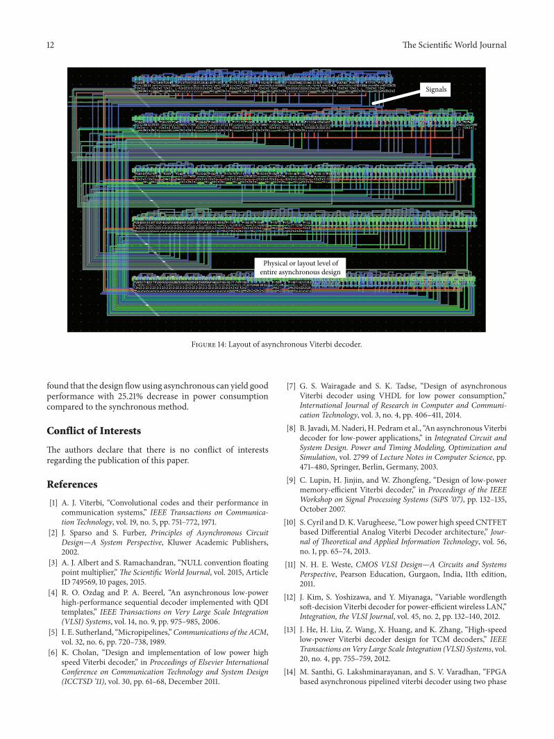
After the completion of the architectural design andsimulation, layout of the asynchronous design is generatedfrom the microwind tool by extracting the spice netlist asgiven in Figure 14. The layout of the chip has an area of2700𝜇m × 2700𝜇m. Various optimizations are done at thislevel like slack optimization in ACS and SMU unit of thedecoder. All the components in the proposed design are auto-matically placed and routed by analyzing the critical path inthe design.The chip of asynchronous design runs at 1.11 times
ahead of its synchronous design because the logic depth isminimum in the critical path due to the DCVSL logic andlack of clock skew.
Table 3 gives the state-of-the-art comparison like tech-nology, number of states, code rate, and maximum speedfrom Kawokgy and Salama [19]. Various parameters of thecomparison show that the proposed asynchronous QDIdesign of Viterbi decoder outperforms the previous designswith an increase in 60% speed and 10% decrease in powerconsumption. Normally, the asynchronous circuits that aredesigned are Delay Insensitive type and each block performsits operation based on the complete signal. Thus, the fre-quency is higher in the proposed asynchronous system thanthe other systems, but in the synchronous circuit, though ofmuch less complexity, due to the clock signals, the powerconsumption is high.
7. Conclusion
Viterbi decoders employed in numerous applications suchas in LANs, ultra wide band systems, and digital mobilecommunications are complex in their implementation and

The Scientific World Journal 11
Table 3: Comparison of parameters of Asynchronous Viterbi decoder with the state of art from existing designs [19].
Parameters Synchronous design Asynchronous design Asynchronous design Asynchronous QDI designTechnology 0.25 um 0.35 um 0.18 um 180 nmNo. of states 64 64 64 64Code rate 1/2 1/2 1/2 1/2Max Speed 200Mb/s 90Mb/s 213Mb/s 433Mb/sAvg. Power 183mW 1333mW 85mW 74.03mW
Cell 0
Cell 0
Cell 0
Cell 0
Cell 0
Cell 0
Cell 0
4.00.0
Time (ns)
4.00.0
Time (ns)
4.00.0
Time (ns)
4.00.0
Time (ns)
4.00.0
Time (ns)
4.00.0
Time (ns)0 50 100 150 200
0 50 100 150 200
0 50 100 150 200
0 50 100 150 200
0 50 100 150 200
0 50 100 150 200
Time (ns)0 50 100 150 200
Out
Req
Ack
b1
b0
a1
a0(V)
Volta
ge
4.00.0(V
)Vo
ltage
(V)
Volta
ge(V
)Vo
ltage
(V)
Volta
ge(V
)Vo
ltage
(V)
Volta
ge
�(out, Vss)
�(b1, Vss)
�(b0, Vss)
�(a1, Vss)
�(a0, Vss)
�(reqin, Vss)
�(ackin, Vss)
Figure 13: Output waveform of asynchronous Viterbi decoder.
they dissipate large power. This paper has presented animproved performance of the Viterbi decoder with asyn-chronous design for constraint length from 𝐾 = 4 to 7. TheViterbi decoder is also applicable for synchronous design, butwith the help of clock signals.ThePCHBandWCHB templatebased asynchronous methodology allows better integrationof blocks running at various speeds. The design highlights
the usage of the library based cells that are used in theconstraint length of 𝐾 = 4 to 7. The simulation is performedusing Tanner Spice in TSMC 0.25𝜇m technology and thedesign also works for other technology files, namely, 65 nmand 180 nm. As the technology increases, asynchronousdesigns are less costly for complex designs which can beconsidered in the long run. From the results, it has been
12 The Scientific World Journal
Signals
Physical or layout level ofentire asynchronous design
Figure 14: Layout of asynchronous Viterbi decoder.
found that the design flowusing asynchronous can yield goodperformance with 25.21% decrease in power consumptioncompared to the synchronous method.
Conflict of Interests
The authors declare that there is no conflict of interestsregarding the publication of this paper.
References
[1] A. J. Viterbi, “Convolutional codes and their performance incommunication systems,” IEEE Transactions on Communica-tion Technology, vol. 19, no. 5, pp. 751–772, 1971.
[2] J. Sparso and S. Furber, Principles of Asynchronous CircuitDesign—A System Perspective, Kluwer Academic Publishers,2002.
[3] A. J. Albert and S. Ramachandran, “NULL convention floatingpoint multiplier,”The Scientific World Journal, vol. 2015, ArticleID 749569, 10 pages, 2015.
[4] R. O. Ozdag and P. A. Beerel, “An asynchronous low-powerhigh-performance sequential decoder implemented with QDItemplates,” IEEE Transactions on Very Large Scale Integration(VLSI) Systems, vol. 14, no. 9, pp. 975–985, 2006.
[5] I. E. Sutherland, “Micropipelines,”Communications of the ACM,vol. 32, no. 6, pp. 720–738, 1989.
[6] K. Cholan, “Design and implementation of low power highspeed Viterbi decoder,” in Proceedings of Elsevier InternationalConference on Communication Technology and System Design(ICCTSD ’11), vol. 30, pp. 61–68, December 2011.
[7] G. S. Wairagade and S. K. Tadse, “Design of asynchronousViterbi decoder using VHDL for low power consumption,”International Journal of Research in Computer and Communi-cation Technology, vol. 3, no. 4, pp. 406–411, 2014.
[8] B. Javadi,M.Naderi, H. Pedram et al., “An asynchronousViterbidecoder for low-power applications,” in Integrated Circuit andSystem Design. Power and Timing Modeling, Optimization andSimulation, vol. 2799 of Lecture Notes in Computer Science, pp.471–480, Springer, Berlin, Germany, 2003.
[9] C. Lupin, H. Jinjin, and W. Zhongfeng, “Design of low-powermemory-efficient Viterbi decoder,” in Proceedings of the IEEEWorkshop on Signal Processing Systems (SiPS ’07), pp. 132–135,October 2007.
[10] S. Cyril andD. K. Varugheese, “Low power high speedCNTFETbased Differential Analog Viterbi Decoder architecture,” Jour-nal of Theoretical and Applied Information Technology, vol. 56,no. 1, pp. 65–74, 2013.
[11] N. H. E. Weste, CMOS VLSI Design—A Circuits and SystemsPerspective, Pearson Education, Gurgaon, India, 11th edition,2011.
[12] J. Kim, S. Yoshizawa, and Y. Miyanaga, “Variable wordlengthsoft-decision Viterbi decoder for power-efficient wireless LAN,”Integration, the VLSI Journal, vol. 45, no. 2, pp. 132–140, 2012.
[13] J. He, H. Liu, Z. Wang, X. Huang, and K. Zhang, “High-speedlow-power Viterbi decoder design for TCM decoders,” IEEETransactions on Very Large Scale Integration (VLSI) Systems, vol.20, no. 4, pp. 755–759, 2012.
[14] M. Santhi, G. Lakshminarayanan, and S. V. Varadhan, “FPGAbased asynchronous pipelined viterbi decoder using two phase

The Scientific World Journal 13
bundled-data protocol,” in Proceedings of the IEEE Interna-tional SoC Design Conference (SOCC ’08), vol. 1, pp. I-314–I-317, BEXCO Conference Center, Busan, Republic of Korea,November 2008.
[15] X. Wang, Y. Zhang, and H. Chen, “Design of viterbi decoderbased on FPGA,” Physics Procedia, vol. 24, pp. 1243–1247, 2012.
[16] T. Kalavathi Devi and C. Venkatesh, “Low power VLSI archi-tecture of a Viterbi decoder using asynchronous prechargehalf buffer dual rail techniques,” Georgian Electronic ScientificJournal: Computer Science and Telecommunications, vol. 34, pp.3–16, 2012.
[17] T. Kalavathi Devi and C. Venkatesh, “Design of low powerViterbi decoder using asynchronous techniques,” InternationalJournal on Advances in Engineering and Technology, vol. 4, pp.561–570, 2012.
[18] P. Sreenivasulu, S. Rao, andV. Babu, “Ultra-lowpower designingfor CMOS sequential circuits,” International Journal of Commu-nications, Network and System Sciences, vol. 8, no. 5, pp. 146–153,2015.
[19] M. Kawokgy and C. A. T. Salama, “Low-power asynchronousViterbi decoder for wireless applications,” in Proceedings of theInternational Symposium on Lower Power Electronics andDesign(ISLPED ’04), pp. 286–289, San Francisco, Calif, USA, August2004.

International Journal of
AerospaceEngineeringHindawi Publishing Corporationhttp://www.hindawi.com Volume 2014
RoboticsJournal of
Hindawi Publishing Corporationhttp://www.hindawi.com Volume 2014
Hindawi Publishing Corporationhttp://www.hindawi.com Volume 2014
Active and Passive Electronic Components
Control Scienceand Engineering
Journal of
Hindawi Publishing Corporationhttp://www.hindawi.com Volume 2014
International Journal of
RotatingMachinery
Hindawi Publishing Corporationhttp://www.hindawi.com Volume 2014
Hindawi Publishing Corporation http://www.hindawi.com
Journal ofEngineeringVolume 2014
Submit your manuscripts athttp://www.hindawi.com
VLSI Design
Hindawi Publishing Corporationhttp://www.hindawi.com Volume 2014
Hindawi Publishing Corporationhttp://www.hindawi.com Volume 2014
Shock and Vibration
Hindawi Publishing Corporationhttp://www.hindawi.com Volume 2014
Civil EngineeringAdvances in
Acoustics and VibrationAdvances in
Hindawi Publishing Corporationhttp://www.hindawi.com Volume 2014
Hindawi Publishing Corporationhttp://www.hindawi.com Volume 2014
Electrical and Computer Engineering
Journal of
Advances inOptoElectronics
Hindawi Publishing Corporation http://www.hindawi.com
Volume 2014
The Scientific World JournalHindawi Publishing Corporation http://www.hindawi.com Volume 2014
SensorsJournal of
Hindawi Publishing Corporationhttp://www.hindawi.com Volume 2014
Modelling & Simulation in EngineeringHindawi Publishing Corporation http://www.hindawi.com Volume 2014
Hindawi Publishing Corporationhttp://www.hindawi.com Volume 2014
Chemical EngineeringInternational Journal of Antennas and
Propagation
International Journal of
Hindawi Publishing Corporationhttp://www.hindawi.com Volume 2014
Hindawi Publishing Corporationhttp://www.hindawi.com Volume 2014
Navigation and Observation
International Journal of
Hindawi Publishing Corporationhttp://www.hindawi.com Volume 2014
DistributedSensor Networks
International Journal of