an efficient chiplevel time slack allocation algorithm for dual-vdd fpga power reduction yan lin 1,...
Post on 21-Dec-2015
214 views
TRANSCRIPT

An Efficient Chiplevel Time Slack Allocation Algorithm for Dual-Vdd FPGA Power Reduction
An Efficient Chiplevel Time Slack Allocation Algorithm for Dual-Vdd FPGA Power Reduction
Yan Lin1, Yu Hu1, Lei He1 and Vijay Raghunathan2
1EE Department, UCLA2Purdue University
Partially supported by NSF. Partially supported by NSF.
Address comments to [email protected] comments to [email protected]

OutlineOutline
Background, Motivation and Problem Formulation
Chip-level Vdd-level Assignment Algorithm [for mixed length wire segments, Hu et al, DAC’06]
Network Flow Based Vdd Level Assignment Formulation
Experimental Results
Conclusions

BackgroundBackground
Existing FPGAs are power inefficient compared to ASICs.
Interconnect is the dominant component of FPGA power dissipation (dynamic and leakage). [Li, TCAD‘05]
Power aware FPGA architectures and CAD algorithms have been studied extensively. CAD algorithms to minimize power-delay product
[Lamoureux, ICCAD’03] Configuration inversion for leakage reduction
[Anderson, FPGA’04] Vdd-programmable FPGA logic blocks [Li, FPGA’04] [Li, DAC’04] Vdd-programmable FPGA interconnects [Li, ICCAD’04] [Gayasen, FPL’04] [Anderson, ICCAD’04] [Lin, DAC’05]

Island style and mixed wire segment length.
Routing switch/connection block (Two PMOS power transistors M3 and M4 are inserted between the tri-state buffer and VddH, VddL power rails, respectively.) [Li, ICCAD’04]
Level converter free in routing tree (Guarantee that no VddL switch
drives VddH switches.) with LEAST area and power penalty[Lin, TCAD’06].
Vdd Programmable Interconnect Arch.Vdd Programmable Interconnect Arch.

1
10
100
1000
10000
1 2 3 4 5 6 7 8 9 1011121314151617181920
CL
B#
1
10
100
1000
10000
100000
Ru
nti
me
(s)
CLB#
runtime
Limitation of Existing ApproachesLimitation of Existing Approaches
Uniform wire segment length was assumed, and cannot be extended to mixed wire segment directly.
LP based formulation is timing consuming and computational instable.
Computational instability: small size circuit uses long runtime
Time consuming: runtime goes up quickly for large circuit

Problem Formulations Problem Formulations
[ Dual-Vdd Level Assignment Problem ]
Given: placement and routing results of a FPGA design
Find: A Vdd-level assignment to each interconnect switch
Objective: Minimize interconnect (dynamic and leakage) power
Constraints: Meet the delay target Tspec
Vdd-level converters are inserted ONLY at CLB inputs/outputs

OutlineOutline
Background, Motivation and Problem Formulation
Chip-level Vdd-level Assignment Algorithm [for mixed length wire segments, Hu et al, DAC’06] Interconnect Power Reduction Estimation LP Based Vdd-level Assignment Algorithm
Network Flow Based Vdd Level Assignment Formulation
Experimental Results
Conclusions

Delay and Power Model for InterconnectDelay and Power Model for Interconnect
Delay Model Intrinsic delay and effective driving resistance of
switch has been pre-characterized using SPICE. Elmore delay is used to calculate routing delay.
Interconnect Power Model Dynamic power Pd(Vddjj)=0.5fclk*C*Vddjj
2
Leakage power Pl(Vddjj) is pre-characterized using SPICE
Interconnect power reduction estimation is the essential part of dual-Vdd assignment algorithm.

Review of Vdd Level Assignment Algorithm [Lin, DAC'05]Review of Vdd Level Assignment Algorithm [Lin, DAC'05]
Chip-level timing slack allocation (LP)
Net-level Bottom-up Vdd assignment
Refinement
Interconnect Vdd assignment
...
...
The net-level bottom-up Vdd assignment guarantees the
legalization of final solutions.[Lin, DAC’05]
Leverage all extra slack with VddL switches
[Lin, DAC’05]
f(1) = .5f(2) = 1f(3) = 1f(4) = 1.5
VddL possibility for switches S2=3
S1=1
b1
b2
b3
b4
Timing Slack assigned at sinks
S2=3S1=1
b1
b2
b3
b4
Vdd assignment base on estimation
Plr(j)=f(j)*ΔPlr(j)
Pdr(j)=0.5fclk*C(j)* f(j)*ΔVdd2
Power reduction estimation
Interconnect power reduction estimation
Problem remained: How to calculate VddL possibility for
mixed wire segment?

VddL Possibility CalculationVddL Possibility Calculation
Represent timing slack in number of switches: si = Li * ( Si / Di )
si is the number of VddL switches can be inserted in the path from source to jth sink in the routing tree.
Li is the number of switches along this path. si : how many switches can be turned to VddL along source-
to-sink-i path for the given timing slack Si.
VddL possiblity for switch j at sink i based on load capacity: f(i,j) = si * (cij / Ci) Key idea: distribute timing slack to each switch based on cap.
L2 = 3D2 = 12s2 = 3*(10/12)=5/2
S2=10
S1=6
b1, 8x
b2, 8x
b3, 16x
b4, 16x f(2,2) = 1f(2,3) = 1f(2,4) = 1/2

Power Reduction Estimation for Mixed Wire SegmentsPower Reduction Estimation for Mixed Wire Segments
The lower bound estimation [Y. Lin, DAC'05] for interconnect power reduction is no longer valid for mixed wire segments.
Our solution: develop the upper bound estimation of VddL switch number
Consistent upper bound of power reduction Remove the non-linear term "min" and the corresponding extra
LP constraints from lower bound estimation
S = 2.7
b2, 8x, need 1.0 slack
b1, 16x, need 1.8 slackfn(i,1) = 0.9
fn(i,2) = 0.5lower bound of VddL switches = 0.9 + .5 = 1.4
S = 2.7
Consume 1.0
Sum up all VddL possibility
1.7 slack left -1.8 needed!
Only 1.0 VddL switch assignment
Problem here: Lower bound > actual number!

LP formulation for dual-Vdd Level AssignmentLP formulation for dual-Vdd Level Assignment
Basic timing constraints
Slack constraints
Objective function Dynamic power reduction upper bound
Leakage power reduction upper bound
Slack upper bound
Slack constraints
Slack non-negative
Arrival time for prim-output
Arrival time for prim-input
Arrival time constraints

OutlineOutline
Motivation
Problem Formulations
Chip-level Vdd-level Assignment Algorithm [for mixed length wire segments, Hu et al, DAC’06]
Network Flow Based Vdd Level Assignment Formulation Overview of network flow based timing slack budgeting Primal-dual reformulation
Experimental Results
Conclusions

Network Flow Based Timing Slack BudgetingNetwork Flow Based Timing Slack Budgeting
Motivated by [Ghiasi, ICCAD’04] for logic level optimization
Step 1: Reorganize objective function:
Step 2: Eliminate timing slack variables (by substitution):
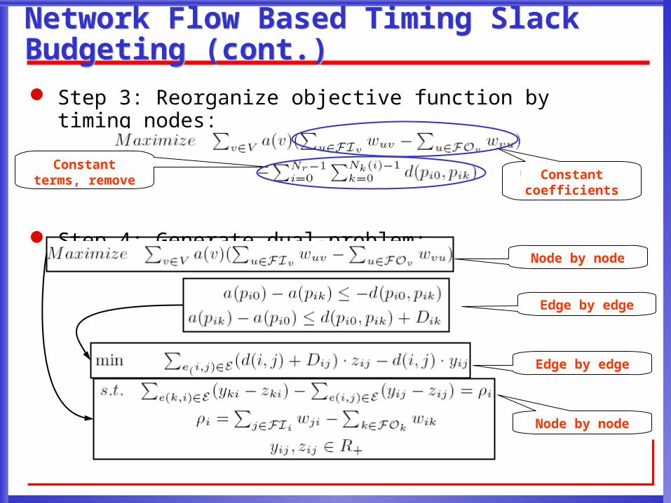
Network Flow Based Timing Slack Budgeting (cont.)Network Flow Based Timing Slack Budgeting (cont.)
Step 3: Reorganize objective function by timing nodes:
Step 4: Generate dual-problem:
Constant terms, remove Constant
coefficients
Node by node
Edge by edge
Node by node
Edge by edge

Link Induced Network from Timing GraphLink Induced Network from Timing Graph
00
-9-9
-3/3-2/2
-1
-4-2
-2/2
-3
-1/1
-3
0
-1
-4
-6
-9
9
-7
0
-9
Flow in forward arch(solid segments)
Flow in backward arch (dot segments)
Demand in node i
No negative weight cycle exists in the induced network. A min-cost flow can be found for sure!
A shortest path based algorithm is used to produce the solution for primal problem.

OutlineOutline
Motivation
Problem Formulations
Chip-level Vdd-level Assignment Algorithm [for mixed length wire segments, Hu et al, DAC’06]
Network Flow Based Formulation
Experimental Results
Conclusions

Experimental SettingExperimental Setting
Cluster-based Island Style FPGA Structure Size-10 cluster and size-4 LUT 100% buffered interconnects, subset switch block 60% length-4 and 40% length-8l wire segments 25x buffer for length-4 and 10x buffer for length-8
ITRS 100nm technology, 1.3v for VddH and 0.8v for VddL
Use VPR [Betz-Rose-Marquardt] for placement and routing
Use fpgaEva-LP2 [Lin et al, FPGA’05] for power calculation Considering short-circuit power, glitch power and input vector 8% average error compared to SPICE simulation
20 biggest sequential MCNC benchmarks are tested
Use LPsolver to solve LP

Both LP-based and Netflow-based algorithm achieves 85% VddL assignment on average.
Dual-Vdd Assignment for FPGAs with Mixed Wire SegmentsDual-Vdd Assignment for FPGAs with Mixed Wire Segments
0.00%
20.00%
40.00%
60.00%
80.00%
100.00%
120.00%
ex5p
apex
4
mise
x3alu
4se
q
apex
2de
ssp
la
ex10
10 pdc
tseng ds
ipdif
feq
s298
bigke
y
ellipt
icfri
sc
s385
84.1
s384
17clm
a
LP based
Netflow Based

Interconnect Power ReductionInterconnect Power Reduction
Interconnect dynamic power
00.010.020.030.040.050.060.070.08
ex5p
apex
4
mise
x3 alu4
seq
apex
2de
ssp
la
ex10
10 pdc
tseng ds
ipdif
feq
s298
bigke
y
ellipt
icfri
sc
s385
84.1
s384
17clm
a
Single-Vdd
Dual-Vdd
Interconnect leakage power
00.0010.0020.0030.0040.0050.0060.0070.0080.009
ex5p
apex
4
mise
x3 alu4
seq
apex
2de
ssp
la
ex10
10 pdc
tseng ds
ipdif
feq
s298
bigke
y
ellipt
icfri
sc
s385
84.1
s384
17clm
a
Single-Vdd
Dual-Vdd
52% total interconnect
power reduction is achieved!

Runtime comparisonRuntime comparison
Runtime (timing slack budgeting)
1
10
100
1000
10000
100000
Ru
nti
me
(s)
Network flow based
LP based
Runtime (overall)
1
10
100
1000
10000
100000
Ru
nti
me
(s)
Network flow based
LP based
Netflow based algorithm gets
consistent speedup and
stable runtime
More significant speedup is
expected for larger circuits.
OutlineOutline
Motivation
Problem Formulations
Chip-level Vdd-level Assignment Algorithm [for mixed length wire segments]
Network Flow Based Formulation
Experimental Results
Conclusions

ConclusionsConclusions
A min-cost network flow based timing budgeting formulation which speedups up the budgeting procedure and the overall design flow up to 6000x and 20x, respectively, compared to LP based one.
Both chip-level dual-Vdd assignment algorithms are for mixed length wire segment. Experimental results show an interconnect power reduction of 53% on average compared to single-Vdd FPGA designs.

Thank you!
Q/A