an efficient strategy to generate high resolution three ... · pdf fileswitching scheme based...
TRANSCRIPT

International Journal of Computer and Electrical Engineering, Vol. 2, No. 3, June, 2010 1793-8163
413
Abstract—Pulse Width Modulation (PWM) is a common
technique used in many different applications. This technique is the heart of the inverter system. This paper reported a modified strategy in asynchronous unipolar sinusoidal PWM (SPWM) switching scheme based on ACEX1K50TC144-3 Altera Field Programmable Gate Array (FPGA). The carrier frequency was designed for 20 kHz and the fundamental frequency was designed to adjust 1 to 100 Hz, with step increase in 1 Hz. A new SPWM signal generation strategy is proposed and compared to traditional SPWM generation technique. The design entry is conducted by Max+plus II version 10.2 through schematic and VHDL programming. The verification in level simulation and hardware realization has been done. As the result, the proposed modified SPWM signal generation strategy works properly and can reduces the usage of logic cell (LC) until 63.75%.
Index Terms—Drive, FPGA, inverter, PWM.
I. INTRODUCTION Pulse Width Modulation (PWM) has become the facto in
industrial standard. PWM is a common technique used in many different applications. This technique is the heart of the inverter system control signal. Up to now, many types of modulating modes have been brought forward in motion control and power conversion, such as sinusoidal PWM, space vector PWM, current tracking PWM, harmonic elimination PWM and so on [1, 2, 3, 4]. These methods have some advantages and disadvantages, but the most widely techniques used are the sinusoidal PWM and the space vector PWM.
Most of these PWM techniques are realized by software and motion control Application-Specific Integrated Circuit (ASIC). There are also some analog circuits in ASIC. ASIC is a very good approach to generate PWM signals; its’ performance and cost have challengeable advantages. However, their design is limited by semiconductor manufacturers and the users cannot change their functions. The most famous SPWM ASICs include Siemens SLE4520, Marconi MA818, and Phillips HEF4752V. They are
Manuscript received August 13, 2009. This work was supported in part by the Competition Grant Research
(PHB) scheme on the 2006-2007 years, the Directorate General of Higher Education, Ministry of National Education, Republic of Indonesia.
Tole Sutikno is with the Department of Electrical Engineering, Faculty of Industrial Technology, Universitas Ahmad Dahlan (UAD), Yogyakarta, Indonesia e-mail: [email protected] or [email protected]
Mochammad Facta is with the Department of Electrical Engineering, Faculty of Engineering, Universitas Diponegoro (UNDIP), Semarang, Indonesia, e-mail: [email protected] or [email protected]
successful as the total digital control IC, and they can be used independently as well as incorporated into a microprocessor-based system [5]. But the switching frequency can be up to 1000Hz, so it is only suitable for low speed power devices as BJT and GTO, not for IGBT or MOSFET.
Many efforts have been conducted to make strategies of PWM generation in analog or digital domain. The digital PWM generation techniques have successfully eliminated the component drift and tolerance problems associated with earlier analogue implementation. The digital designs based on FPGA have been used successfully in many different electric system applications such as in power converter PWM inverter. Speed performance is considered as an appropriate solution in order to boost the performance of controllers for industrial control systems as an effort to reduce the gap between the analog and digital world [6, 7]. Designing a PWM inverter drive using FPGA has several advantages, such as quick, modifiable, and suitable for prototyping.
The PWM technique has been the subject of intensive research. Recently several researches were conducted in generating PWM with FPGA. De Castro, et al [8] who had created single PWM based on XC3S200-4FT256 Spartan FPGA by using the DLL (or PLL) available in almost FPGA for single phase inverter drive. Md Isa, et al [9] had created unipolar SPWM for single phase inverter drive based on FPGA, but they did not state what type of the FPGA was used. The design and simulation is conducted by using Max Plus II software. However, the unipolar SPWM method offers a good opportunity for the realization of the inverter control [10].
This paper has proposed a new unipolar SPWM signal generation strategy for three phase inverter drive based on FPGA. By using the higher carrier frequency and the proper ratio of carrier and modulated reference frequency, this method has possibility to reduce the harmonics in three phase converter. Also by using only 1/6 segments of modulating signal in each phase, it is expected that this technique can reduce the usage of logic cells (LCs) in the Altera FPGA, and the memory requirements.
II. THREE PHASE SPWM SIGNAL GENERATION TECHNIQUE In conventional method, SPWM uses a sinusoidal
modulator and a triangular carrier wave. By comparing these two signals, the control pulses of each inverter branch are determined. The conventional SPWM generation technique
An Efficient Strategy to Generate High Resolution Three-Phase Pulse Width Modulation Signal Based on Field Programmable Gate Array
Tole Sutikno, Member, IACSIT & IEEE, Mochammad Facta, Member, IEEE

International Journal of Computer and Electrical Engineering, Vol. 2, No. 3, June, 2010 1793-8163
414
is shown in Fig. 1. Fig. 2 shows a diagram block of high resolution conventional three phases SPWM signal generation based on FPGA.
Fig. 1. Conventional SPWM generation technique.
Fig. 2. Diagram block of high resolution traditional three phase SPWM
signal generation based on FPGA
III. PROPOSED SPWM SIGNAL GENERATION STRATEGY The developed SPWM is based on symmetrical sampling.
The triangular carrier and the sinusoidal modulating signal are used. The principle of proposed SPWM signal generation is improved and based on conventional SPWM generation technique, with each phase is divided into 600 segments; the SPWM is generated for the first 600 by storing samples to form a three phase modulating signal as shown in Fig. 3. This technique is possible to reduce the usage of LCs in Altera FPGA. The decoding of the look-up table to form the full
wave of the three phase modulating signals is shown in Table 1.
Fig. 3. The only first 600 sine waveform is used in the proposed SPWM
generation
TABLE 1. DECODING OF LOOK-UP TABLE Angle (0) A phase B phase C phase
0-60 a c b 60-120 -c -b -a 120-180 b a c 180-240 -a -c -b 240-300 c b a 300-360 -b -a -c
IV. HARDWARE IMPLEMENTATION In this work, the proposed SPWM strategies is done using
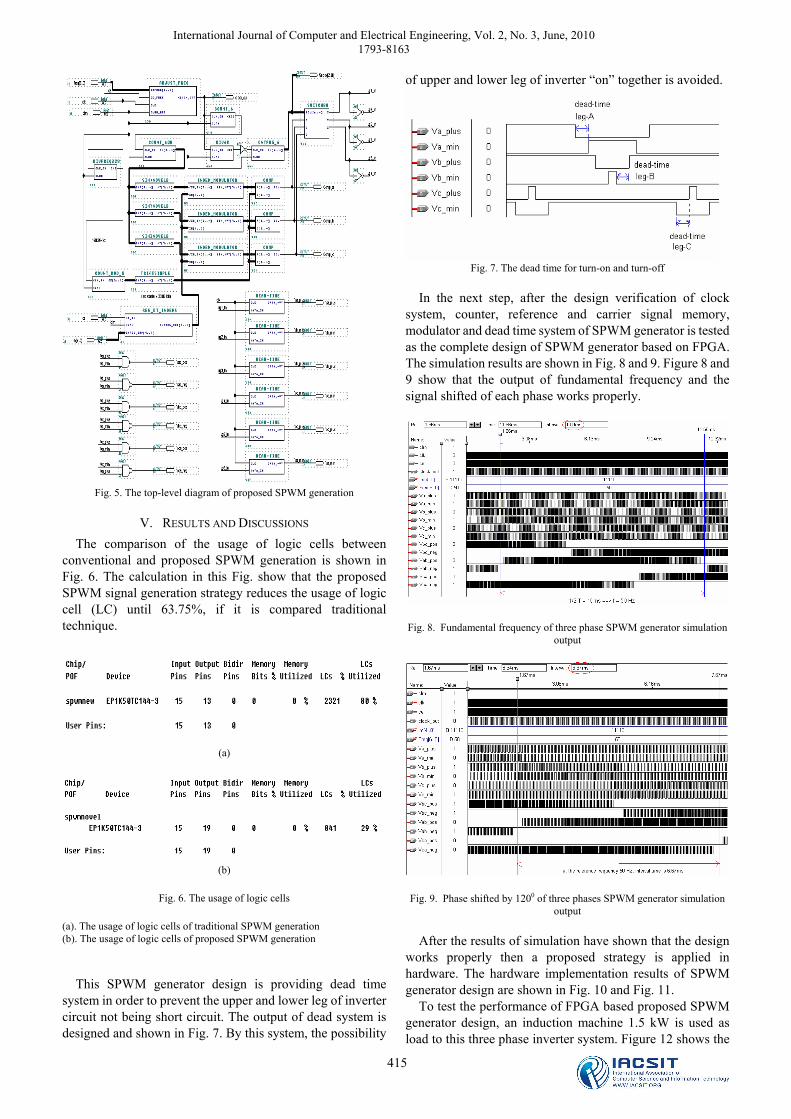
Max+plus II Baseline version 10.2, which is the Altera development tool. Its converts the design idea into configuration data files, and it is loaded to the Altera FPGA device. The ACEX1KTC50144-3 Altera FPGA is used in this research. The top-level diagram of traditional SPWM generation is shown in Fig. 4. Fig. 5 shows the top-level diagram of proposed SPWM generation.
Fig. 4. The top-level diagram of traditional SPWM generation
International Journal of Computer and Electrical Engineering, Vol. 2, No. 3, June, 2010 1793-8163
415
Fig. 5. The top-level diagram of proposed SPWM generation
V. RESULTS AND DISCUSSIONS The comparison of the usage of logic cells between
conventional and proposed SPWM generation is shown in Fig. 6. The calculation in this Fig. show that the proposed SPWM signal generation strategy reduces the usage of logic cell (LC) until 63.75%, if it is compared traditional technique.
(a)
(b)
Fig. 6. The usage of logic cells
(a). The usage of logic cells of traditional SPWM generation (b). The usage of logic cells of proposed SPWM generation
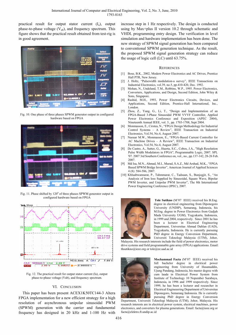
This SPWM generator design is providing dead time system in order to prevent the upper and lower leg of inverter circuit not being short circuit. The output of dead system is designed and shown in Fig. 7. By this system, the possibility
of upper and lower leg of inverter “on” together is avoided.
Fig. 7. The dead time for turn-on and turn-off
In the next step, after the design verification of clock
system, counter, reference and carrier signal memory, modulator and dead time system of SPWM generator is tested as the complete design of SPWM generator based on FPGA. The simulation results are shown in Fig. 8 and 9. Figure 8 and 9 show that the output of fundamental frequency and the signal shifted of each phase works properly.
Fig. 8. Fundamental frequency of three phase SPWM generator simulation output
Fig. 9. Phase shifted by 1200 of three phases SPWM generator simulation
output After the results of simulation have shown that the design
works properly then a proposed strategy is applied in hardware. The hardware implementation results of SPWM generator design are shown in Fig. 10 and Fig. 11.
To test the performance of FPGA based proposed SPWM generator design, an induction machine 1.5 kW is used as load to this three phase inverter system. Figure 12 shows the
International Journal of Computer and Electrical Engineering, Vol. 2, No. 3, June, 2010 1793-8163
416
practical result for output stator current (Ia), output phase-to-phase voltage (Vab), and frequency spectrum. This figure shows that the practical result obtained from test-rig is in good agreement.
Fig. 10. One phase of three phases SPWM generator output in configured hardware based on FPGA
Fig. 11. Phase shifted by 1200 of three phases SPWM generator output in configured hardware based on FPGA
Fig. 12. The practical result for output stator current (Ia), output phase-to-phase voltage (Vab), and frequency spectrum.
VI. CONCLUSION This paper has been present ACEX1K50TC144-3 Altera
FPGA implementation for a new efficient strategy for a high resolution of asynchronous unipolar sinusoidal PWM (SPWM) generation with the carrier and fundamental frequency has designed in 20 kHz and 1-100 Hz with
increase step in 1 Hz respectively. The design is conducted using by Max+plus II version 10.2 through schematic and VHDL programming entry design. The verification in level simulation and hardware implementation has been done. The new strategy of SPWM signal generation has been compared to conventional SPWM generation technique. As the result, the proposed SPWM signal generation strategy can reduce the usage of logic cell (LC) until 63.75%.
REFERENCES [1] Bose, B.K., 2002, Modern Power Electronics and AC Drives, Prentice
Hall PTR, New Jersey. [2] J. Holtz, “Pulsewidth modulation-a survey”, IEEE Transactions on
Industrial Electronics, vol.39, no.5, pp.410-420, Dec. 1992. [3] Mohan, N., Undeland, T.M., Robbins, W.P., 1995. Power Electronics,
Converters, Applications, and Design, Second Edition, John Wiley & Sons, Singapore.
[4] Rashid, M.H., 1993, Power Electronics Circuits, Devices, and Applications, Second Edition, Prentice-Hall International, Inc., London.
[5] Zhou, Z., Yang, G., Li, T., “Design and Implementation of an FPGA-Based 3-Phase Sinusoidal PWM VVVF Controller, Applied Power Electronics Conference and Exposition (APEC 2004), Nineteenth Annual IEEE, vol. 3., pp. 1703-1708, Sept 2004.
[6] Monmasson, E., Cirstea, N., “FPGA Design Methodology for Industrial Control Systems – A Review”, IEEE Transaction on Industrial Electronics, Vol.54, No.4, August 2007.
[7] Naouar M.W., Monmasson, E., “FPGA-Based Current Controller for AC Machine Drives – A Review”, IEEE Transaction on Industrial Electronics, Vol.54, No.4, August 2007.
[8] De Castro, A., Sutter, G., Huerta, S.C., Cobos, J.A., "High Resolution Pulse Width Modulators in FPGA", Programmable Logic, 2007. SPL '07. 2007 3rd Southern Conference on, vol., no., pp.137-142, 28-26 Feb. 2007.
[9] Md Isa, M.N., Ahmad, M.I., Murad, S.A.Z., Md Arshad, M.K., “FPGA Based SPWM Bridge Inverter”, American Journal of Applied Sciences 4 (8): 584-586, 2007.
[10] Khluabwannarat, P., Tahmmarat, C., Tadsuan, S., Bunjogjit, S., “An Analysis of Iron loss Supplied by Sinusoidal, Square Wave, Bipolar PWM Inverter, and Unipolar PWM Inverter”, The 8th International Power Engineering Conference (IPEC), 2007.
Tole Sutikno (M’07 IEEE) received his B.Eng. degree in electrical engineering from Diponegoro University (UNDIP), Semarang, Indonesia, his M.Eng. degree in Power Electronics from Gadjah Mada University UGM), Yogyakarta, Indonesia, in 1999 and 2004, respectively. Since 2001 he has been a lecturer in Electrical Engineering Department, Universitas Ahmad Dahlan (UAD), Yogyakarta, Indonesia. He is currently pursuing PhD degree in Energy Conversion Department, Universiti Teknologi Malaysia (UTM), Johor,
Malaysia. His research interests include the field of power electronics, motor drive systems and field programmable gate array (FPGA) applications. Email: [email protected] or [email protected]
Mochammad Facta (M’07 IEEE) received his full bachelor degree in electrical power engineering from University of Hasanuddin, Ujung Pandang, Indonesia, his master degree with cum laude in Electrical Power System from Institute of Technology 10 Nopember Surabaya, Indonesia, in 1996 and 1999 respectively. Since 1999, he has been a lecturer and researcher in Electrical Engineeering Department of Universitas Diponegoro, Semarang Indonesia. He is currently pursuing PhD degree in Energy Conversion
Department, Universiti Teknologi Malaysia (UTM), Johor, Malaysia. His research interests are in electrical power system, electrical machines, power electronics, and converters for plasma generations. Email: [email protected] or [email protected]