an energy-efficient reconfigurable public-key cryptography
TRANSCRIPT

1808 IEEE JOURNAL OF SOLID-STATE CIRCUITS, VOL. 36, NO. 11, NOVEMBER 2001
An Energy-Efficient Reconfigurable Public-KeyCryptography Processor
James Goodman, Member, IEEE,and Anantha P. Chandrakasan, Member, IEEE
Abstract—The ever-increasing demand for security in portableenergy-constrained environments that lack a coherent securityarchitecture has resulted in the need to provide energy-effi-cient algorithm-agile cryptographic hardware. Domain-specificreconfigurability is utilized to provide the required flexibility,without incurring the high overhead costs associated with genericreprogrammable logic. The resulting implementation is capableof performing an entire suite of cryptographic primitives over theintegers modulo , binary Galois Fields and nonsupersingularelliptic curves over GF(2 ), with fully programmable moduli,field polynomials and curve parameters ranging in size from 8to 1024 bits. The resulting processor consumes a maximum of75 mW when operating at a clock rate of 50 MHz and a 2-Vsupply voltage. In ultralow-power mode (3 MHz at 0.7 V) theprocessor consumes at most 525W. Measured performance andenergy efficiency indicate a comparable level of performance topreviously reported dedicated hardware implementations, whileproviding all of the flexibility of a software-based implementation.In addition, the processor is two to three orders of magnitude moreenergy efficient than optimized software and reprogrammablelogic-based implementations.
I. INTRODUCTION
T HE FIELD of cryptographic algorithms can be dividedinto two basic types, symmetric and asymmetric, which
have distinctly different properties. Symmetric, or secret-key,algorithms require two parties to share some secret piece of in-formation (i.e., the key) that is then used to encrypt/decrypt mes-sages between them. The existence of a shared piece of secretinformation enables secret-key algorithms to be very computa-tionally efficient. Hence, symmetric algorithms are used to en-crypt the bulk of the messages being passed. Asymmetric, orpublic-key, algorithms on the other hand rely on the presumedexistence of hard number-theoretic problems that enable twosets of keys to be created: public (encryption) and private (de-cryption). Public keys are stored in the open so that anyone canencrypt a message. However, because of the number-theoreticproperties of the algorithms used, only the intended recipientwho generated the public–private key pair can decode the mes-sage correctly. Hence, no secret needs to be shared by the com-municating parties. Unfortunately, the underlying mathematics
Manuscript received March 22, 2001; revised June 4, 2001. This workwas supported in part by the Defense Advanced Research Project Agency(DARPA) Power Aware Computing/Communication Program and the Air ForceResearch Laboratory, Air Force Materiel Command, USAF, under agreementF30602-00-2-0551, and in part by National Semiconductor Corporation.
J. Goodman is with Chrysalis-ITS, Ottawa, ON K2G 6P9, Canada.A. P. Chandrakasan is with the Massachusetts Institute of Technology, Cam-
bridge, MA 02139 USA.Publisher Item Identifier S 0018-9200(01)08228-2.
which enables this asymmetry requires a great deal more com-putation than symmetric-key algorithms. For example, a singlepublic-key operation can consume as much time and energy asencrypting tens of megabits using a secret-key cipher. Thus,public-key algorithms are used primarily for establishing se-cret keys throughout the network in a secure manner, as well asfor user authentication and identification. The work describedwithin this paper addresses the implementation of public-keycryptographic algorithms only.
In the past, several standards for implementing various asym-metric techniques have been proposed, leading to a multitude ofincompatible systems that are based upon different underlyingmathematical problems and algorithms. For example, the IEEE1363 Standard Specification for Public Key Cryptography [1]recognizes three distinct families of problems upon which to im-plement asymmetric techniques: integer factorization (IF), dis-crete logarithms (DL), and elliptic curves (EC).
As a result, system developers have had to utilize software-based techniques in order to achieve the algorithm agility re-quired to maintain compatibility. Unfortunately, software-basedapproaches lead to slow implementations that are very energyinefficient. Hence, these approaches are not well suited to themigration to portable battery-operated nomadic computing ter-minals. Hardware-based implementations, on the other hand,while being very energy and computationally efficient, are veryinflexible and capable of supporting only a limited subset ofasymmetric cryptography. A compromise between these twoextremes is achieved by taking advantage of the fact that therange of operations is small enough that domain-specific recon-figurable hardware can be developed that is capable of imple-menting the various asymmetric algorithms without incurringthe overhead associated with generic reconfigurable logic de-vices. Furthermore, this is done in an energy-efficient mannerthat enables operation in the portable energy-constrained envi-ronments where this algorithm agility is required most of all.The resulting implementation is known as the domain-specificreconfigurable cryptographic processor (DSRCP).
In conventional reconfigurable applications such as field-pro-grammable gate arrays (FPGAs), the architectural goals ofthe device are to provide a large number of small yet pow-erful programmable logic cells, embedded within a flexibleprogrammable interconnect. Unfortunately, the overhead asso-ciated with making such a general purpose computing deviceultimately limits its energy efficiency and hence its utility inenergy-constrained environments. Kusse [2] quantifies thisoverhead by breaking down the energy consumption of aconventional FPGA (Xilinx XC4003A [3]) into its architectural
0018–9200/01$10.00 © 2001 IEEE

GOODMAN AND CHANDRAKASAN: ENERGY-EFFICIENT RECONFIGURABLE PUBLIC-KEY CRYPTOGRAPHY PROCESSOR 1809
TABLE IDSRCP INSTRUCTIONSET
components. The analysis reveals that only 5% of the totalenergy is used to perform useful computation, while approxi-mately 65% is dissipated in the programmable interconnect.
The DSRCP differs from conventional reconfigurable imple-mentations in that its reconfigurability is limited to the subsetof functions, called a domain, required for asymmetric cryptog-raphy as defined in IEEE 1363. This domain requires only asmall set of configurations for performing all of the requiredoperations over all possible problem families defined withinthe standard. As a result, the reconfiguration overhead, particu-larly that of the reprogrammable interconnect, is much smallerin terms of performance, energy efficiency, and reconfigurationtime, making the DSRCP feasible for algorithm-agile asym-metric cryptography in energy-constrained environments.
II. A RCHITECTURE
A. Instruction Set Architecture
The instruction set definition of the DSRCP is dictated by theIEEE 1363 Public Key Cryptography Standard document [1]. Alist of the arithmetic functions required to implement the various
Fig. 1. Top-level system architecture.
primitives defined in the standard was tabulated in a functionalmatrix, which was then used to define the instruction set archi-tecture (ISA) of the processor (Table I). The ISA contains 24 in-structions broken up into six types of operations: conventionalarithmetic, modular integer arithmetic, GF arithmetic, el-liptic curve field arithmetic over GF , register manipulation,and processor configuration.

1810 IEEE JOURNAL OF SOLID-STATE CIRCUITS, VOL. 36, NO. 11, NOVEMBER 2001
Fig. 2. Hierarchical instruction structure of the DSRCP.
B. Hardware Architecture
Fig. 1 shows a top-level block diagram of the DSRCP. Theprocessor consists of four main architectural blocks: the globalcontroller and microcode ROMs, the I/O interface, the shutdowncontroller, and the reconfigurable datapath.
The global microcontroller is responsible for all high-levelcontrol within the DSRCP. The controller utilizes a three-tieredcontrol approach that uses both hardwired and microsequencedcontrol functions. This multitiered approach is required asvarious instructions within the DSRCP’s ISA are implementedusing other instructions, as illustrated by the MOD_MULTinstruction example shown in Fig. 2.
The microcode approach is used due to its simplicity and ex-tensibility, as modifications and enhancements of the ISA canbe accomplished with minimal design effort by modifying themicrocode ROM. The drawback of using this approach is theadditional latency that is incurred by accessing the ROMs se-quentially, which can end up consuming a significant portion ofthe processor’s cycle time. This performance issue is addressedby pipelining the instruction decoding/sequencing at the outputof the first-level microcode ROM, as shown in Fig. 2.
The DSRCP features a shutdown controller that is respon-sible for disabling unused portions of the datapath in order tominimize any unnecessary switched capacitance. The shutdownstrategy is dictated by the current width of the datapath, as setby the last invocation of the SET_LENGTH instruction and en-ables the datapath to be shut down in 32 32-b increments.
Operands used within the processor can vary in size from8 to 1024 bits (1025 bits in the case of field polynomials forGF ), requiring the use of a flexible I/O interface that al-lows the user to transfer data to/from the processor in a veryefficient manner. Ultimately, the I/O interface width is dictatedby the physical implementation of the processor, which makes a32-b interface the most economical width. The choice of a 32-binterface maps well to existing systems, as well as allowing forrelatively fast operand transfer onto and off of the processor, re-quiring at most 32 cycles to transfer the largest possible operand.The additional bit required for GF field polynomials isinput as part of the REG_LOAD instruction word.
The primary component of the DSRCP is the reconfigurabledatapath, whose architecture is shown in Fig. 3. The datapathconsists of four major functional blocks: an eight-word registerfile, a fast adder unit, a comparator unit, and the main reconfig-urable logic unit.
The register file size is chosen to be eight words as that is theminimum number required to implement all of the functions of
Fig. 3. Reconfigurable datapath architecture block diagram.
the datapath. The limiting case for this architecture is that of el-liptic curve point multiplication in which registers R2 and R3are used to store the point that is going to be multiplied by thevalue stored in Exp register, R4 and R5 are used to store theresult, R0 and R1 are used to store an intermediate point usedduring the computation, R6 is used to store the curve parameter, and R7 is used as a dummy register in order to provide re-
silience to timing attacks. The number of read and write portswithin the register file is dictated by the requirement to be ableto perform single-cycle two-operand instructions that generatea writeback value. In certain cases, two write ports could haveproven useful (e.g., elliptic curve point transfers), but the infre-quency of the operation did not merit the additional overheadthat it would have introduced.
The fast adder unit is capable of adding/subtracting two-bit( ) operands in three cycles using the hybridcarry–bypass and carry–select technique described in [4] andoptimized for a bitsliced implementation (Fig. 4).
The comparator unit performs single-cycle magnitudecomparisons between two-bit operands, as well as computingthe XOR of the two operands (i.e., GF addition). Thecomparator generates two flags,and , that can be decodedinto all possible magnitude relations.
The reconfigurable logic unit consists of six local registers(Pc, Ps, A, B, Exp, and N) and a reconfigurable logic block thatis capable of implementing all of the required datapath oper-ations. The Pc and Ps registers are used primarily in modularoperations to store the carry–save format partial product and inGalois Field operations as two separate temporary values. A andB store the input operands used in all modular and Galois Field

GOODMAN AND CHANDRAKASAN: ENERGY-EFFICIENT RECONFIGURABLE PUBLIC-KEY CRYPTOGRAPHY PROCESSOR 1811
Fig. 4. Modified bitsliced carry–bypass adder [4].
operations. The Exp register is used for storing either the expo-nent value in the case of exponentiation operations or the mul-tiplier value in the case of elliptic curve point multiplication.The N register also serves a dual purpose; for modular opera-tions it is used as the modulus value, and in Galois Field opera-tions, it stores the field polynomial in a binary vector form (e.g.,
is stored as [10000101]). In all relevant operations,it is assumed that both the Exp and N registers are preloadedwith their required values.
Using local memory within the datapath eliminates the needto continually access the register file every cycle, eliminatingthe associated overhead of repeated register file accesses andminimizing the amount of reprogrammable interconnect by ef-fectively isolating the reconfigurable logic from the rest of theprocessor. In addition, several operations requires four registerreads and two writes in any given cycle, requiring additionalread and write ports to be added to the register file. This wouldin turn increase the size of the register file, as well as its de-coding complexity, thereby offsetting any advantage that mightbe gained by going to a unified memory model that eliminatesthe local memory.
The datapath utilizes three separate busses for distributingdata between the various functional units: the two operandbusses ( and ) and the writeback bus ( ). Not allregisters and busses are interconnected, as analysis dictated thatnot all connections were required. The unnecessary connectionsare removed in order to minimize the capacitive load on thebusses. is also used as a secondary writeback bus to enablevalues within the datapath to be transferred between the localregisters.
III. A LGORITHM IMPLEMENTATION
The DSRCP performs a variety of algorithms rangingfrom modular integer arithmetic to elliptic curve arithmeticover GF . All operations are universal in that they can beperformed using any valid -bit modulus ( ),GF field polynomial and nonsupersingular elliptic curveover GF . Given the wide range of functionality, some
explanation regarding how the various algorithms are imple-mented is warranted.
A. Modular Arithmetic
The various complex modular arithmetic operations (mul-tiplication, reduction, inversion, and exponentiation) areimplemented using microcode, while simple operations (ad-dition and subtraction) are implemented directly in hardwareusing the wide adder and comparator units. Multiplication isperformed using Montgomery multiplication [5], which com-putes the value MONTMULT mod .An additional Montgomery multiplication with a correctionfactor of mod is then performed to undo the division by
inherent in Montgomery’s method. The correction factoris assumed to be preloaded into the register file and is thenspecified via a third source operand ( ) in the instructionword. Modular reduction is performed using a similar techniquewith Montgomery reduction at its core.
Modular inverses are computed using the extended binary eu-clidean algorithm [6]. This technique requires special architec-tural considerations, such as the ability to right shift the outputof the adder unit, and explicit access to the LSB of R1, R2, andR3 in order to check the looping conditions of the algorithm.
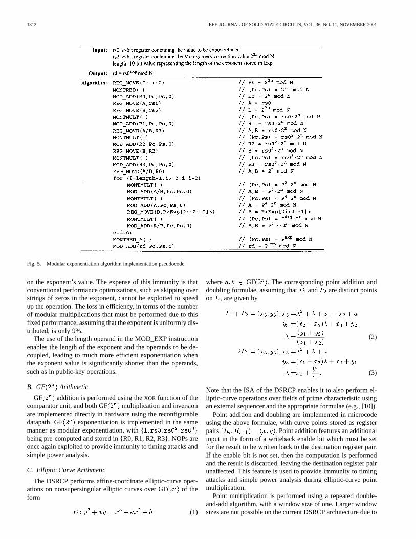
Modular exponentiation is performed using a standardsquare-and-multiply algorithm [7] with an exponent scanningwindow of size two. The algorithm (Fig. 5) precomputesand stores the values { }in {R0, R1, R2, R3}, respectively. During each iteration, thecurrent value is squared twice and then the exponent is scannedtwo bits at a time. Scanning is done nondestructively soexponent values need not be reloaded prior to each operation.The value read corresponds to the register that is used duringthe subsequent multiplication (e.g., if “01” is read, then R1 isused).
Note that multiplication by R0 is essentially a null operation(NOP) due to Montgomery multiplication’s implicit division by
. The use of NOPs provides protection from timing attacks[8],and simple power analysis [9] as a multiplication is always per-formed, thereby eliminating any variation in execution based
1812 IEEE JOURNAL OF SOLID-STATE CIRCUITS, VOL. 36, NO. 11, NOVEMBER 2001
Fig. 5. Modular exponentiation algorithm implementation pseudocode.
on the exponent’s value. The expense of this immunity is thatconventional performance optimizations, such as skipping overstrings of zeros in the exponent, cannot be exploited to speedup the operation. The loss in efficiency, in terms of the numberof modular multiplications that must be performed due to thisfixed performance, assuming that the exponent is uniformly dis-tributed, is only 9%.
The use of the length operand in the MOD_EXP instructionenables the length of the exponent and the operands to be de-coupled, leading to much more efficient exponentiation whenthe exponent value is significantly shorter than the operands,such as in public-key operations.
B. GF Arithmetic
GF addition is performed using theXOR function of thecomparator unit, and both GF multiplication and inversionare implemented directly in hardware using the reconfigurabledatapath. GF exponentiation is implemented in the samemanner as modular exponentiation, with { }being pre-computed and stored in {R0, R1, R2, R3}. NOPs areonce again exploited to provide immunity to timing attacks andsimple power analysis.
C. Elliptic Curve Arithmetic
The DSRCP performs affine-coordinate elliptic-curve oper-ations on nonsupersingular elliptic curves over GF of theform
(1)
where GF . The corresponding point addition anddoubling formulae, assuming that and are distinct pointson , are given by
(2)
(3)
Note that the ISA of the DSRCP enables it to also perform el-liptic-curve operations over fields of prime characteristic usingan external sequencer and the appropriate formulae (e.g., [10]).
Point addition and doubling are implemented in microcodeusing the above formulae, with curve points stored as registerpairs . Point addition features an additionalinput in the form of a writeback enable bit which must be setfor the result to be written back to the destination register pair.If the enable bit is not set, then the computation is performedand the result is discarded, leaving the destination register pairunaffected. This feature is used to provide immunity to timingattacks and simple power analysis during elliptic-curve pointmultiplication.
Point multiplication is performed using a repeated double-and-add algorithm, with a window size of one. Larger windowsizes are not possible on the current DSRCP architecture due to

GOODMAN AND CHANDRAKASAN: ENERGY-EFFICIENT RECONFIGURABLE PUBLIC-KEY CRYPTOGRAPHY PROCESSOR 1813
Fig. 6. Shutdown circuitry used in the DSRCP.
TABLE IIDSRCP INSTRUCTIONMAPPING WITHIN THE CONTROL HIERARCHY
memory limitations of the register file (e.g., four precomputedvalues would require eight additional registers). The issue oftiming attacks is once again addressed by using NOPs via thewriteback enable bit of the point addition operation. The over-head associated with using NOPs is 33% relative to a conven-tional implementation where NOPs are skipped, and 50% if asigned radix-2 representation is used for the multiplier [7].
IV. I MPLEMENTATION
A. Controller and Microcode ROMs
The instruction set partitioning of the three-level control hi-erarchy is shown in Table II. The first tier of control corre-sponds to those instructions that are implemented directly inhardware. The second tier of control represents the first levelof microcoded instructions that are composed of sequences offirst-tier instructions. Similarly, the third tier of control repre-sents instructions that consist of sequences of both first- andsecond-tier instructions.
Each microcode controller consists of a small ROM core, aninput selector which gates the appropriate values onto the corre-sponding operand signals, and a control FSM that also serves asthe ROM address generator. The resulting controllers emulatesmall microcontrollers. The microcode ROMs are implementedusing static ROMs which eliminate the need for any prechargedcircuit techniques, making for a more robust implementation atthe cost of requiring complementary word-select lines and largerbit cells due to the use of larger pMOS devices. However, giventhe small size of the ROMs and their relatively low duty cycle,the resulting energy and area overhead penalties are much lessthan 0.1% of the total DSRCP area and energy consumption.
Fig. 7. Power consumption as a function of processor width.
B. Shutdown Controller
The shutdown controller is capable of shutting down the data-path row by row, in 32-b increments using both clock and controlsignal gating, which is performed using simpleAND structuresin the row drivers that are found along the inside edge of the twohalves of the datapath, as shown in Fig. 6. All clock gating sig-nals are generated off the falling edge of the main clock to ensurethat edge-triggered signals generated from the main clock (e.g.,register file clocks) are gated during the low phase of the clockto eliminate any spurious glitches that may occur byANDing theclock with a late-arriving enable signal while the clock is high.
The result of this shutdown strategy is a linear reduction inpower consumption as a function of the datapath width, as illus-trated in Fig. 7.
There is a subtle feature of the shutdown control scheme, dueto the way Galois Field multiplication is performed within theDSRCP, that warrants additional explanation. When performingoperations over the field GF , the field polynomial is an thdegree polynomial that is stored as an ( ) bit value. Hence,enabling only the least significantbits of the datapath may re-sult in errors, as the effects of the MSB may not be accountedfor if the MSB lies within a disabled portion of the datapath.This condition occurs when is a multiple of 32, so the shut-down controller detects this condition and enables an additional32-b block. Given the operand sizes that are typically used when
1814 IEEE JOURNAL OF SOLID-STATE CIRCUITS, VOL. 36, NO. 11, NOVEMBER 2001
Fig. 8. Adder unit bitslice.
Fig. 9. Tree-based magnitude comparator topology used in the DSRCP.
this condition will occur (512–1024-b), the overhead associatedwith enabling an additional datapath block is on the order of3%–6% extra energy consumption.
C. I/O Interface
The processor’s floorplan is based on two banks of processingelements (PEs), each with 16 rows of 32 processing elements, asshown in Fig. 6. Each bank contains a set of 32-bit-wide verti-cally routed input and output busses. Separate input and outputbusses are used to enable static bus repeaters/latches to be in-serted into the busses at the vertical midpoint of the two banks,allowing the bus to be segmented in order to minimize the ca-pacitive load seen by any given driver on the bus. This allowsminimum sized drivers to be used and eliminates unnecessarycharging/discharging of large portions of the bus capacitance bynear-end drivers. The serpentine distribution of PEs within thedatapath causes each row to be flipped in relation to those aboveand below it. A single level of output muxes at the chip interface
is used to reverse the order of both the input and output bussesas required to provide a consistent 32-b interface at the pads.
D. Reconfigurable Datapath—Register File
The register file is implemented using TSPC-style registers[11]. A more typical SRAM-based register file design was notused due to the small number of registers required and the in-creased robustness of using an edge-triggered memory element.The drawback of this approach is an increase in both area andenergy consumption. The energy consumption penalty is neg-ligible as the register file is accessed very infrequently due tothe local data storage in the reconfigurable logic unit. The areapenalty is more significant as the TSPC register is twice as largeas a simple 6T SRAM cell. Given that the register file repre-sents 20% of the bitslice area, the area overhead is 10%, whichis deemed acceptable for this application.
The register outputs are driven onto the and sourceoperand busses via two 8-to-1 passgate multiplexors and their

GOODMAN AND CHANDRAKASAN: ENERGY-EFFICIENT RECONFIGURABLE PUBLIC-KEY CRYPTOGRAPHY PROCESSOR 1815
(a) (b)
Fig. 10. Multiplier architectures for (a) modular multiplication and (b) GF(2 ) multiplication.
Fig. 11. Extended binary euclidean algorithm used for GF(2 ) inversion operation.
inputs are all connected to the writeback bus. The eight regis-ters feature individual clock and reset lines, with the clock linesalso serving as the writeback register select lines. As mentionedbefore, the register file features architectural features to improvethe efficiency of the modular inversion operation by having R0having a reset value of 1 and providing the LSBs of R0, R1, R2,and R3 to the global control logic.
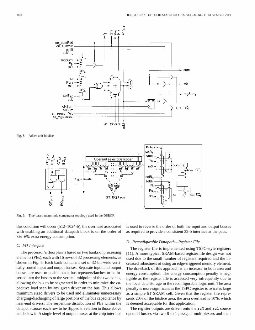
E. Reconfigurable Datapath—Wide Adder Unit
The design requirements for the DSRCP call for a wide addercapable of performing 1024-b binary addition/subtraction in atmost three processor cycles, using an area-efficient bitslicedimplementation with a minimal amount of long interconnect.The area and interconnect requirements precluded the use ofconventional structures such as carry–lookahead, hierarchicalcarry–select, and carry–bypass/skip implementations. However,the modified carry–bypass/skip adder proposed in [4] yields acritical path of approximately 45 full adder delays for a 1024-boperation, while mapping to a very efficient bitsliced implemen-tation. The main difference between this adder and that of a con-ventional implementation is the serialization of the group prop-
agation signal generation within the bitslices of the group. Dis-tributing the propagation signal generation in this manner elimi-nates the need to have a wide fan-inAND gate and allows each bitwithin the group to determine whether the group carry-in will af-fect its output. Hence, each block can generate its valid sum out-puts oneXOR delay after the carry-in is valid. By matching de-lays through proper group sizing, the carry-in becomes valid justas the group propagate and generate signals are valid, leading tothe minimal overall adder delay.
The adder unit bitslice is shown in Fig. 8. The adder con-sists of the aforementioned modified carry–bypass/skip addercell, a local register for storing intermediate results and mul-tiplexors for both input operand selection and right shifting ofthe result. Both the output of the adder (sum) and its registeredversion (regSum) can be driven onto either the or write-back busses. The B input selection muxes utilize a left-shiftedversion of the Pc operand to simplify the conversion of the re-dundant carry–save value stored in (Pc,Ps) into a nonredundantbinary form. Note that the A operand’s signal path includes atristate buffer which is required to eliminate the race conditionthat results when the A operand is read from thebus and the
1816 IEEE JOURNAL OF SOLID-STATE CIRCUITS, VOL. 36, NO. 11, NOVEMBER 2001
Fig. 12. Basic GF(2 ) inversion architecture and resulting datapath cell.
Fig. 13. Reconfigurable logic bitslice.
adder’s nonregistered output is then driven onto the same bus.The tristate buffer breaks the feedback path.
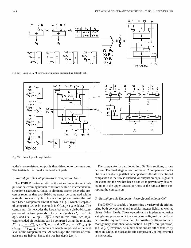
F. Reconfigurable Datapath—Wide Comparator Unit
The DSRCP controller utilizes the wide comparator unit out-puts for determining branch conditions within a microcoded in-struction’s execution. Hence, to eliminate branch delays the pro-cessor requires that two 1024-b operands be compared withina single processor cycle. This is accomplished using the fasttree-based comparator circuit shown in Fig. 9 which is capableof comparing two -bit operands in gate delays. Thecomparator first encodes the inputs based on a bit-by-bit com-parison of the two operands to form the signals opop and op op . Once in this form, two adja-cent encoded bit positions can be compared using the relations
and, the outputs of which are passed to the next
level of the comparator tree. At each stage, the number of com-parisons are halved, hence the tree has depth .
The comparator is partitioned into 32 32-b sections, or oneper row. The final stage of each of these 32 comparator blocksutilizes an enable signal that either performs the aforementionedcomparison if the row is enabled, or outputs an equal signal inthe event that the row has been disabled to prevent any data re-maining in the upper unused portions of the register from cor-rupting the comparison.
G. Reconfigurable Datapath—Reconfigurable Logic Cell
The DSRCP is capable of performing a variety of algorithmsusing both conventional and modular integer fields, as well asbinary Galois Fields. These operations are implemented usinga single computation unit that can be reconfigured on the fly toperform the required operation. The possible configurations areMontgomery multiplication/reduction, GF multiplication,and GF inversion. All other operations are either handled byother units (e.g., the fast adder and comparator), or implementedin microcode.
GOODMAN AND CHANDRAKASAN: ENERGY-EFFICIENT RECONFIGURABLE PUBLIC-KEY CRYPTOGRAPHY PROCESSOR 1817
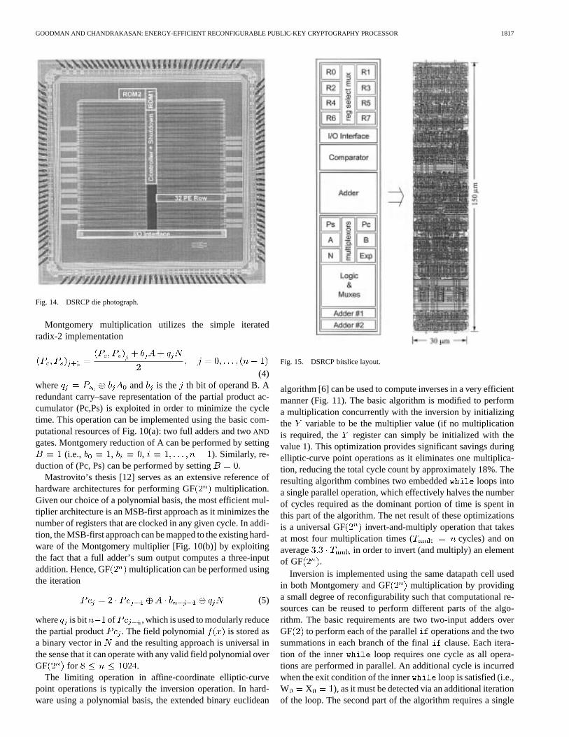
Fig. 14. DSRCP die photograph.
Montgomery multiplication utilizes the simple iteratedradix-2 implementation
(4)where and is the th bit of operand B. Aredundant carry–save representation of the partial product ac-cumulator (Pc,Ps) is exploited in order to minimize the cycletime. This operation can be implemented using the basic com-putational resources of Fig. 10(a): two full adders and twoAND
gates. Montgomery reduction of A can be performed by setting(i.e., , , ). Similarly, re-
duction of (Pc, Ps) can be performed by setting .Mastrovito’s thesis [12] serves as an extensive reference of
hardware architectures for performing GF multiplication.Given our choice of a polynomial basis, the most efficient mul-tiplier architecture is an MSB-first approach as it minimizes thenumber of registers that are clocked in any given cycle. In addi-tion, the MSB-first approach can be mapped to the existing hard-ware of the Montgomery multiplier [Fig. 10(b)] by exploitingthe fact that a full adder’s sum output computes a three-inputaddition. Hence, GF multiplication can be performed usingthe iteration
(5)
where is bit of , which is used to modularly reducethe partial product . The field polynomial is stored asa binary vector in and the resulting approach is universal inthe sense that it can operate with any valid field polynomial overGF for .
The limiting operation in affine-coordinate elliptic-curvepoint operations is typically the inversion operation. In hard-ware using a polynomial basis, the extended binary euclidean
Fig. 15. DSRCP bitslice layout.
algorithm [6] can be used to compute inverses in a very efficientmanner (Fig. 11). The basic algorithm is modified to performa multiplication concurrently with the inversion by initializingthe variable to be the multiplier value (if no multiplicationis required, the register can simply be initialized with thevalue 1). This optimization provides significant savings duringelliptic-curve point operations as it eliminates one multiplica-tion, reducing the total cycle count by approximately 18%. Theresulting algorithm combines two embedded loops intoa single parallel operation, which effectively halves the numberof cycles required as the dominant portion of time is spent inthis part of the algorithm. The net result of these optimizationsis a universal GF invert-and-multiply operation that takesat most four multiplication times ( cycles) and onaverage in order to invert (and multiply) an elementof GF .
Inversion is implemented using the same datapath cell usedin both Montgomery and GF multiplication by providinga small degree of reconfigurability such that computational re-sources can be reused to perform different parts of the algo-rithm. The basic requirements are two two-input adders overGF to perform each of the parallel operations and the twosummations in each branch of the final clause. Each itera-tion of the inner loop requires one cycle as all opera-tions are performed in parallel. An additional cycle is incurredwhen the exit condition of the inner loop is satisfied (i.e.,W X ), as it must be detected via an additional iterationof the loop. The second part of the algorithm requires a single

1818 IEEE JOURNAL OF SOLID-STATE CIRCUITS, VOL. 36, NO. 11, NOVEMBER 2001
TABLE IIIREPORTEDIMPLEMENTATIONS OFMODULAR EXPONENTIATION FUNCTIONS
Fig. 16. Performance of several DSRCP arithmetic instructions.
Fig. 17. Performance of various cryptographic primitives using the DSRCP at50 MHz.
Fig. 18. Comparison of energy consumption per operation for software,FPGA, and DSRCP.
cycle as well. The two datapath adders can be used as two-inputGF adders by zeroing one of their inputs and then utilizingmultiplexors to allow the adder inputs to be changed on the fly.The corresponding architecture and its resulting mapping to thedatapath cell is shown in Fig. 12.
The final reconfigurable datapath cell is shown in Fig. 13 andcontains two reconfigurable full adders, twoAND gates, and sixlocal register cells with multiplexed inputs. The reconfigurableadders are implemented using high-performance small-areapass-transistor-based full-adder cells with multiplexed inputs.The adder and register reconfiguration muxes are configuredthrough the use of eight control lines, three for the adder muxesand five for the register muxes, that are exposed to the controlhardware, allowing for single-cycle reconfigurability.

GOODMAN AND CHANDRAKASAN: ENERGY-EFFICIENT RECONFIGURABLE PUBLIC-KEY CRYPTOGRAPHY PROCESSOR 1819
V. EXPERIMENTAL RESULTS AND EVALUATION
The processor is fabricated in a 0.25-m CMOS technologywith five levels of metallization. Fig. 14 depicts a micropho-tograph of the processor whose core contains 880 000 devicesand measures 2.92.9 mm . The datapath consists of 1024processing bitslices, each of which measures 30150 m(Fig. 15). At 50 MHz, the processor operates at a supplyvoltage of 2 V and consumes at most 75 mW of power. Inultralow-power mode (3 MHz at V), the processorconsumes at most 525W.
Fig. 16 shows the performance of those DSRCP instructionswhose execution time is proportional to the size of the operands.The results are normalized relative to the operand size in orderto better illustrate this proportionality. The performance of thecryptographic primitives required for IF, DL, and EC-basedcryptography are shown in Fig. 17. Important performancepoints are denoted and compared with other reported imple-mentations in Table III. The DSRCP’s performance comparesfavorably; although several solutions quote higher rates, theyrepresent dedicated solutions with no algorithm agility. Forthose dedicated solutions that report their power consumption,the energy consumption per operation of the DSRCP is foundto be at least a factor of two better.
Fig. 18 demonstrates the energy efficiency of theDSRCP relative to software-based implementations on theStrongARM SA-1100 [13] and previously reported pro-grammable-logic-based implementations ([14], [15]) on XilinxXC4000 parts. The software-based energy consumption is mea-sured using a StrongARM SA-1100 evaluation platform that isexecuting hand-optimized assembly language implementationsof the various cryptographic primitives. The FPGA-basedenergy consumption is estimated using the implementationdetails provided in [14] and [15] and the power consumptionguidelines described in [16]. The DSRCP is approximatelytwo to three orders of magnitude more energy efficient thanboth software and programmable-logic-based solutions, whileproviding the same degree of flexibility and algorithm agility.
VI. CONCLUSION
Given a specific domain of functionality such as public-keycryptography, it is possible to provide a limited degree of do-main-specific reconfigurability to provide flexibility while min-imizing the overhead that is typically associated with repro-grammable logic. Domain specific integrated circuits (DSICs)utilize interconnect-centric architectures to exploit locality inorder to minimize the interconnection overhead, which is thedominant source of energy consumption in generic reconfig-urable logic.
The resulting public-key cryptography DSIC provides a com-parable level of performance and twice the energy efficiencyas previously reported dedicated hardware solutions, while pro-viding all of the flexibility of a software-based implementation.In addition, the processor is two to three orders of magnitudemore energy efficient than both optimized software and repro-grammable-logic-based implementations.
ACKNOWLEDGMENT
The authors would like to thank the National SemiconductorCorporation for providing fabrication facilities.
REFERENCES
[1] Standard Specifications for Public Key Cryptography—Draft 13, IEEEP1363, Nov. 1999.
[2] E. Kusse and J. Rabaey, “Low-energy embedded FPGA structures,”in Proc. 1998 Int. Symp. Low Power Electronic Design (ISLPED), pp.155–160.
[3] “XC4000 field programmable gate arrays: programmable logic data-book,” Xilinx Corp., San Jose, CA, 1996.
[4] A. Satohet al., “A high-speed small RSA encryption LSI with low powerdissipation,” inProc. 1st Int. Information Security Workshop (ISW’97),pp. 174–187.
[5] P. Montgomery, “Modular multiplication without trial division,”Math.Comput., vol. 48, pp. 243–264, 1987.
[6] D. E. Knuth,The Art of Computer Programming—Seminumerical Algo-rithms, 2nd ed. Reading, MA: Addison-Wesley, 1981, vol. 2.
[7] D. M. Gordon, “A survey of fast exponentiation methods,”J. Algo-rithms, vol. 27, no. 1, pp. 129–146, Apr. 1998.
[8] P. Kocher, “Timing attacks on implementations of Diffie-Hellman,RSA, DSS and other systems,” inProc. Advances in Cryptology(CRYPTO’96), pp. 104–113.
[9] P. Kocher, J. Jaffe, and B. Jun. (1998) Introduction to differential poweranalysis and related attacks. [Online]. Available: http://www.cryptog-raphy.com/dpa/technical
[10] G. Seroussi, N. P. Smart, and I. F. Blake,Elliptic Curve Cryptog-raphy. Cambridge, U.K.: Cambridge Univ. Press, 2000.
[11] J. Yuan and C. Svensson, “High-speed CMOS circuit technique,”IEEEJ. Solid-State Circuits, pp. 62–70, Feb. 1989.
[12] E. D. Mastrovito, “VLSI architectures for computation in Galois fields,”Ph.D. dissertation, Linköping Univ., Linköping, Sweden, 1991.
[13] “StrongARM SA-1100 microprocessor for portable applications briefdatasheet,” Intel Corp., Chandler, AZ, 1999.
[14] T. Blum, “Modular exponentiation on reconfigurable hardware,”Master’s thesis, Worcester Polytechnic Inst., Worcester, MA, 1999.
[15] M. C. Rosner, “Elliptic curve cryptosystems on reconfigurable hard-ware,” Master’s thesis, Worcester Polytechnic Inst., Worcester, MA,1998.
[16] “A simple method of estimating power in XC4000Xl/EX/E FPGAs,”Xilinx Corp., San Jose, CA, Application Brief XBRF 014 v1.0, 1997.
[17] S. Ishii, K. Ohyama, and K. Yamanaka, “A single-chip RSA processorimplemented in a 0.5-mm rule gate array,” inProc. 7th Annu. IEEE Int.ASIC Conf. Exhibit, 1994, pp. 433–436.
[18] P. A. Ivey, S. N. Walker, J. M. Stern, and S. Davidson, “An ultrahigh-speed public-key encryption processor,” inProc. IEEE 1992 CustomIntegrated Circuits Conference (CICC’92), pp. 19.6.1–19.6.4.
[19] H. Orup, E. Svendsen, and E. Andreasen, “VICTOR: an efficient RSAhardware implementation,” inProc. Advances in Cryptography (EURO-CRYPT’90), pp. 245–252.
[20] P. -S Chen, S. -A Hwang, and C. -W Jen, “A systolic RSA public-keycryptosystem,” in Proc. IEEE Int. Symp. Circuits and Systems(ISCAS’96), pp. 408–411.
[21] C.-C. Yang, T.-S. Chang, and C.-W. Jen, “A new RSA cryptosystemhardware design based on montgomery’s algorithm,”IEEE Trans. Cir-cuits Syst. II, vol. 45, pp. 908–913, July 1998.
[22] J.-H. Guo, C.-L. Wang, and H.-C. Hu, “Design and implementation of anRSA public-key cryptosystem,” inProc. 1999 IEEE Int. Symp. Circuitsand Systems (ISCAS’99), vol. 1, pp. 504–507.
[23] J.-Y. Leu and A.-Y. Wu, “A scalable low-complexity digit-serial VLSIarchitecture for RSA cryptosystem,” in1999 IEEE Workshop SignalProcessing Systems (SIPS’99), pp. 586–595.
[24] A. Roya, J. Moran, and J. C. Lopez, “Design and implementation of aco-processor for cryptography applications,” inProc. 1997 EuropeanDesign and Test Conf. (ED&TC’97), pp. 213–217.
[25] A. Vandemeulebroecke, “A single-chip 1024-bits RSA processor,” inProc. Advances in Cryptology (EUROCRYPT’89), pp. 219–236.
[26] M. Shand and J. Vuillemin, “’Fast implementations of RSA cryptog-raphy,” in Proc. 11th IEEE Symp. Computer Arithmetic, 1993, pp.252–259.
[27] D. Yuliang, M. Zhigang, Y. Yizheng, and W. Tao, “Implementation ofRSA cryptoprocessor based on Montgomery algorithm,” inProc. 5th Int.Conf. Solid-State and Integrated Circuit Technology, 1998, pp. 524–526.
[28] H. Garner, “The residue number system,”IRE Trans. Electron. Comput.,vol. EC-8, pp. 140–147, 1959.
1820 IEEE JOURNAL OF SOLID-STATE CIRCUITS, VOL. 36, NO. 11, NOVEMBER 2001
James Goodman(S’97–M’00) received the B.A.Sc.degree in electrical engineering from the Universityof Waterloo, Waterloo, ON, Canada, in 1994. He re-ceived the S.M. and Ph.D. degrees in electrical en-gineering and computer science from the Massachu-setts Institute of Technology, Cambridge, in 1996 and2000, respectively. His primary research areas werereconfigurable energy-efficient architectures for im-plementing cryptographic algorithms and protocols.
He is currently with Chrysalis-ITS, Ottawa, ON,Canada, as Senior IC Security Architect, developing
next-generation integrated-security solutions for a variety of applications. Heis a member of the Signal Processing Subcommittee for the ISSCC 2002, theTechnical Program Committee for VLSI 2001, and the Program Committee forthe Workshop on Cryptographic Hardware and Embedded Systems (CHES).
Dr. Goodman received the 1999 Design Automation Conference Design Con-test Award.
Anantha P. Chandrakasan (S’92–M’95) receivedthe B.S, M.S., and Ph.D. degrees in electrical engi-neering and computer sciences from the Universityof California, Berkeley, in 1989, 1990, and 1994, re-spectively.
Since September 1994, he has been with theMassachusetts Institute of Technology, Cambridge,where he is currently an Associate Professor ofelectrical engineering and computer science. Heheld the Analog Devices Career Development Chairfrom 1994 to 1997. His research interests include
the ultralow-power implementation of custom and programmable digitalsignal processors, distributed wireless sensors, multimedia devices, emergingtechnologies, and CAD tools for VLSI. He is a co-author of the bookLowPower Digital CMOS Design(Norwell, MA: Kluwer) and a co-editor ofLow Power CMOS DesignandDesign of High-Performance MicroprocessorCircuits (New York: IEEE Press). He has served on the technical programcommittee of various conferences including the ISSCC, VLSI Circuits Sym-posium, DAC, and the International Symposium on Low-power Electronicsand Design (ISLPED). He has served as a technical program co-chair for the1997 ISLPED, VLSI Design ’98, and the 1998 IEEE Workshop on SignalProcessing Systems, and as a general co-chair of the 1998 ISLPED. He servedas an elected member of the Design and Implementation of Signal ProcessingSystems (DISPS) Technical Committee of the Signal Processing Society. Hewas the Signal Processing Sub-committee chair for ISSCC 1999 through 2001.He is Program Vice-Chair for the ISSCC 2002.
Dr. Chandrakasan received the NSF Career Development award in 1995, theIBM Faculty Development award in 1995, and the National Semiconductor Fac-ulty Development award in 1996 and 1997. He has received several best paperawards, including the 1993 IEEE Communications Society’s Best Tutorial PaperAward, the IEEE Electron Devices Society’s 1997 Paul Rappaport Award forthe Best Paper in an EDS publication during 1997, and the 1999 Design Au-tomation Conference Design Contest Award. He was an Associate Editor forthe IEEE JOURNAL OF SOLID-STATE CIRCUITS from 1998 to 2001.