an input matched x-band balanced low noise … · an input matched x-band balanced low noise...
TRANSCRIPT
AN INPUT MATCHED X-BAND BALANCEDLOW NOISE AMPLIFIER DESIGN ANDIMPLEMENTATION USING DISCRETE
TRANSISTORS
a thesis submitted to
the graduate school of engineering and science
of bilkent university
in partial fulfillment of the requirements for
the degree of
master of science
in
electrical and electronics engineering
By
Cagdas Ballı
July, 2015
AN INPUT MATCHED X-BAND BALANCED LOW NOISE AM-
PLIFIER DESIGN AND IMPLEMENTATION USING DISCRETE
TRANSISTORS
By Cagdas Ballı
July, 2015
We certify that we have read this thesis and that in our opinion it is fully adequate,
in scope and in quality, as a thesis for the degree of Master of Science.
Prof. Dr. Ekmel Ozbay(Advisor)
Dr. Tarık Reyhan(Co-Advisor)
Prof. Dr. Yusuf Ziya Ider
Assoc. Prof. Dr. Sedat Nazlıbilek
Approved for the Graduate School of Engineering and Science:
Prof. Dr. Levent OnuralDirector of the Graduate School
ii

ABSTRACT
AN INPUT MATCHED X-BAND BALANCED LOWNOISE AMPLIFIER DESIGN AND IMPLEMENTATION
USING DISCRETE TRANSISTORS
Cagdas Ballı
M.S. in Electrical and Electronics Engineering
Advisors: Prof. Dr. Ekmel Ozbay and Dr. Tarık Reyhan
July, 2015
X-Band, which is defined as the frequency range from 8 GHz to 12 GHz by
IEEE, is used for the applications such as satellite communications, radar and
space communications. These applications require an input matched, high gain
and low noise amplifier as a front-end component in their receiver chains. In this
work, an input matched X-Band balanced low noise amplifier is designed and
implemented by using GaAs HJ-FET transistor. Measurements of the fabricated
amplifier show a maximum noise figure of 1.74 dB, a minimum gain of 12.1 dB
and a minimum input return loss of 11.4 dB from 8.2 GHz to 8.4 GHz.
Keywords: low noise amplifier, balanced amplifier, noise figure.
iii

OZET
AYRIK TRANSISTORLER KULLANILARAKX-BANTTA GIRIS EMPEDANS UYUMLU, DENGELI
VE DUSUK GURULTULU YUKSELTEC TASARIMI VEGERCEKLENMESI
Cagdas Ballı
Elektrik ve Elektronik Muhendisligi, Yuksek Lisans
Tez Danısmanları: Prof. Dr. Ekmel Ozbay ve Dr. Tarık Reyhan
Temmuz, 2015
IEEE tarafından 8 GHz ile 12 GHz arasında tanımlanmıs frekans aralıgı olan X-
Bant, uydu haberlesme, radar ve uzay haberlesme gibi uygulamalar tarafından
kullanılan bir banttır. Bu uygulamalar, almac zincirinde uc eleman olarak, giris
empedans uyumlu, yuksek kazanclı ve dusuk gurultulu yukseltece gerek duymak-
tadır. Bu calısmada, X-Bantta giris empedans uyumlu, dengeli, dusuk gurultulu
yukseltec tasarlanmıs ve gerceklenmistir. Uretilen yukseltec, 8.2 - 8.4 GHz
bandında en fazla 1.74 dB gurultu figuru gosterir iken, en az 12.1 dB kazanc
ve en az 11.4 dB giris geri donus kaybı gostermektedir.
Anahtar sozcukler : dusuk durultulu yukseltec, dengeli yukseltec, gurultu figuru.
iv
Acknowledgement
I would like to express my sincere thanks to my advisor Dr. Tarık Reyhan for
his support and guidance throughout my studies in Bilkent. His extensive knowl-
edge and experience has been an invaluable source of inspiration and motivation
for me. I would also thank Prof. Dr. Ekmel Ozbay for his support.
I am also grateful to Prof. Dr. Yusuf Ziya Ider and Assoc. Prof. Dr. Sedat
Nazlıbilek for being a part of my thesis committee.
I owe a great debt of thanks to my awesome family for their constant love,
encouragement, moral support and sacrifices.
I owe my deepest thanks to Tugba Ikiz for her endless support and under-
standing.
v
Contents
1 Introduction 1
2 Background 4
2.1 Definition . . . . . . . . . . . . . . . . . . . . . . . . . . . . . . . 4
2.2 Low Noise Amplifier Concepts . . . . . . . . . . . . . . . . . . . . 5
2.2.1 Equivalent Noise Temperature and Noise Figure . . . . . . 5
2.2.2 Stability . . . . . . . . . . . . . . . . . . . . . . . . . . . . 7
2.2.3 Linearity . . . . . . . . . . . . . . . . . . . . . . . . . . . . 8
2.2.4 Input and Output Matching . . . . . . . . . . . . . . . . . 9
2.3 Balanced Amplifier . . . . . . . . . . . . . . . . . . . . . . . . . . 10
2.4 Simulation Techniques Used . . . . . . . . . . . . . . . . . . . . . 12
2.5 Noise Figure Measurement Techniques . . . . . . . . . . . . . . . 12
2.5.1 Y-Factor Method . . . . . . . . . . . . . . . . . . . . . . . 12
2.5.2 Cold Source Method . . . . . . . . . . . . . . . . . . . . . 15
3 Design and Simulation 16
3.1 Transistor Selection . . . . . . . . . . . . . . . . . . . . . . . . . . 16
3.2 Single-Ended Low Noise Amplifier Design . . . . . . . . . . . . . . 17
3.2.1 Active Bias Circuit . . . . . . . . . . . . . . . . . . . . . . 17
3.2.2 Stability . . . . . . . . . . . . . . . . . . . . . . . . . . . . 18
3.2.3 Input Matching Network . . . . . . . . . . . . . . . . . . . 21
3.2.4 Output Matching Network . . . . . . . . . . . . . . . . . . 24
3.2.5 Final Design and Layout . . . . . . . . . . . . . . . . . . . 26
3.3 Balanced Low Noise Amplifier Design . . . . . . . . . . . . . . . . 30
3.3.1 Active Bias Circuit . . . . . . . . . . . . . . . . . . . . . . 30
vi

CONTENTS vii
3.3.2 Stability . . . . . . . . . . . . . . . . . . . . . . . . . . . . 30
3.3.3 Input Matching Network . . . . . . . . . . . . . . . . . . . 30
3.3.4 Output Matching Network . . . . . . . . . . . . . . . . . . 30
3.3.5 Wilkinson Power Divider/Combiner . . . . . . . . . . . . . 31
3.3.6 Final Design and Layout . . . . . . . . . . . . . . . . . . . 33
4 Measurements 38
4.1 Measurement Preparations and Setups . . . . . . . . . . . . . . . 38
4.1.1 S-Parameter Measurement Setup . . . . . . . . . . . . . . 39
4.1.2 Noise Figure Measurement Setup . . . . . . . . . . . . . . 40
4.1.3 P1dB Measurement Setup . . . . . . . . . . . . . . . . . . . 41
4.1.4 IP3 Measurement Setup . . . . . . . . . . . . . . . . . . . 41
4.2 Measurement Results and Comparison . . . . . . . . . . . . . . . 42
4.2.1 S-Parameter Measurements . . . . . . . . . . . . . . . . . 42
4.2.2 Y-Factor Noise Figure Measurements . . . . . . . . . . . . 44
4.2.3 Cold Source Noise Figure Measurements . . . . . . . . . . 47
4.2.4 P1dB Measurement . . . . . . . . . . . . . . . . . . . . . . 48
4.2.5 IP3 Measurement . . . . . . . . . . . . . . . . . . . . . . . 50
4.2.6 Measurement with an Isolator . . . . . . . . . . . . . . . . 52
4.2.7 Summary . . . . . . . . . . . . . . . . . . . . . . . . . . . 54
5 Conclusion 55

List of Figures
2.1 Balanced amplifier configuration . . . . . . . . . . . . . . . . . . . 10
2.2 Y-factor method . . . . . . . . . . . . . . . . . . . . . . . . . . . 12
2.3 Graphical representation of Y-factor method . . . . . . . . . . . . 14
2.4 Graphical representation of cold-source method . . . . . . . . . . 15
3.1 Active bias circuit . . . . . . . . . . . . . . . . . . . . . . . . . . . 17
3.2 Bias tee . . . . . . . . . . . . . . . . . . . . . . . . . . . . . . . . 18
3.3 µ-parameter before stabilization . . . . . . . . . . . . . . . . . . . 19
3.4 Schematics of the circuit after stabilization . . . . . . . . . . . . . 20
3.5 µ-parameter after stabilization . . . . . . . . . . . . . . . . . . . . 21
3.6 Noise and gain circles before input matching . . . . . . . . . . . . 22
3.7 Input matching network . . . . . . . . . . . . . . . . . . . . . . . 23
3.8 Noise and gain circles after input matching . . . . . . . . . . . . . 23
3.9 Output matching network . . . . . . . . . . . . . . . . . . . . . . 24
3.10 Output impedance before output matching . . . . . . . . . . . . . 25
3.11 Output impedance after output matching . . . . . . . . . . . . . . 25
3.12 Complete schematics of the circuit including Momentum layout . 27
3.13 Simulated µ-parameter of the designed amplifier in Momentum . . 28
3.14 Simulated S-paramters of the designed amplifier in Momentum . . 28
3.15 Simulated noise figure of the designed amplifier in Momentum . . 29
3.16 Final layout of the single-ended low noise amplifier . . . . . . . . 29
3.17 Schematics of the Wilkinson power divider . . . . . . . . . . . . . 31
3.18 Simulation results of Wilkinson power divider . . . . . . . . . . . 32
3.19 Schematics of the final design of the balanced low noise amplifier . 34
3.20 Input and output impedances of the balanced low noise amplifier . 35
viii

LIST OF FIGURES ix
3.21 Simulated µ-parameter of the balanced low noise amplifier designed
in Momentum . . . . . . . . . . . . . . . . . . . . . . . . . . . . . 35
3.22 Simulated S-parameters of the balanced low noise amplifier de-
signed in Momentum . . . . . . . . . . . . . . . . . . . . . . . . . 36
3.23 Simulated noise figure of the balanced low noise amplifier designed
in Momentum . . . . . . . . . . . . . . . . . . . . . . . . . . . . . 36
3.24 Final layout of the balanced low noise amplifier . . . . . . . . . . 37
3.25 Final layout of the active bias circuit . . . . . . . . . . . . . . . . 37
4.1 Fabricated and assembled PCBs . . . . . . . . . . . . . . . . . . . 39
4.2 Metal housing . . . . . . . . . . . . . . . . . . . . . . . . . . . . . 39
4.3 S-Parameters measurement setup . . . . . . . . . . . . . . . . . . 40
4.4 Y-factor noise measurement setup . . . . . . . . . . . . . . . . . . 41
4.5 IP3 measurement setup . . . . . . . . . . . . . . . . . . . . . . . . 42
4.6 S-Parameter measurements of Single-Ended LNA . . . . . . . . . 43
4.7 S-Parameter measurements of Balanced LNA . . . . . . . . . . . . 44
4.8 Y-factor noise figure measurement of Single-Ended LNA . . . . . 45
4.9 Y-factor noise figure measurement of Balanced LNA . . . . . . . . 46
4.10 Cold source noise figure measurement of Single-Ended LNA . . . . 47
4.11 Cold source noise figure measurement of Balanced LNA . . . . . . 48
4.12 OP1dB of Single-Ended LNA . . . . . . . . . . . . . . . . . . . . . 49
4.13 OP1dB of Balanced LNA . . . . . . . . . . . . . . . . . . . . . . . 50
4.14 Two tone intermodulation test of Single-Ended LNA . . . . . . . 51
4.15 Two tone intermodulation test of Balanced LNA . . . . . . . . . . 52
4.16 Single-Ended LNA with an X-band isolator . . . . . . . . . . . . . 53
4.17 Measurement results of Single-Ended LNA with isolator . . . . . . 53
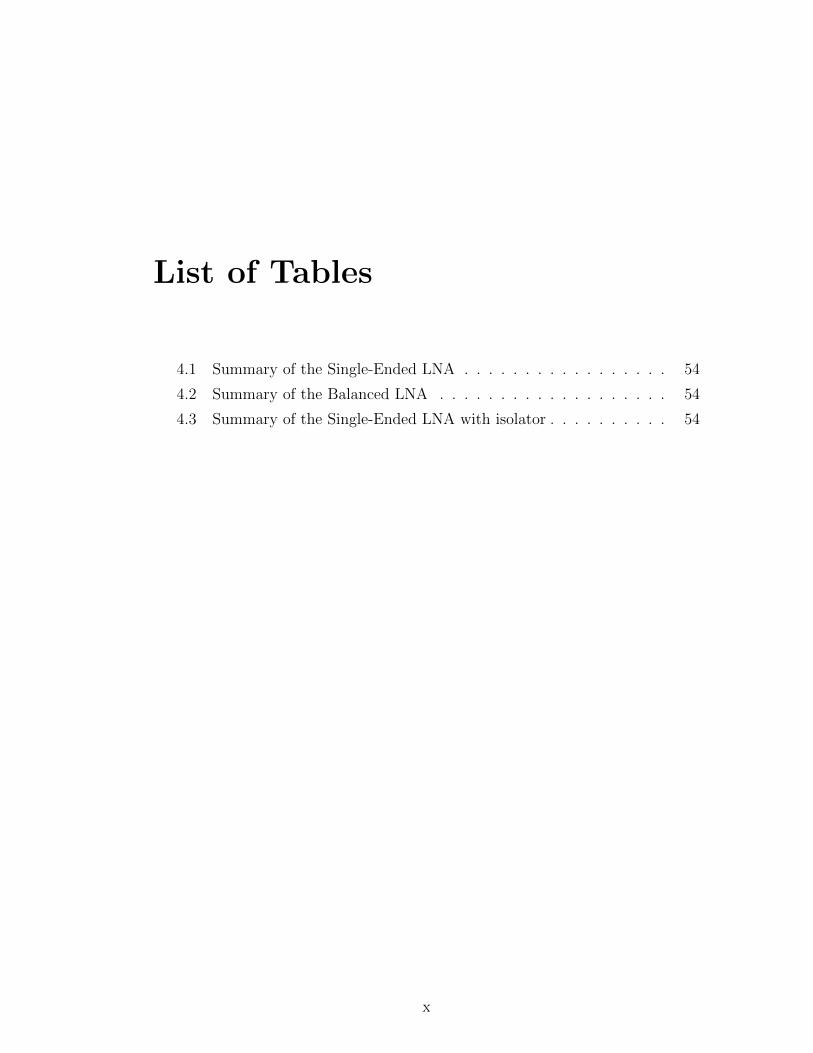
List of Tables
4.1 Summary of the Single-Ended LNA . . . . . . . . . . . . . . . . . 54
4.2 Summary of the Balanced LNA . . . . . . . . . . . . . . . . . . . 54
4.3 Summary of the Single-Ended LNA with isolator . . . . . . . . . . 54
x

Chapter 1
Introduction
X-Band is defined as the frequency range from 8 GHz to 12 GHz by IEEE. Well-
known applications in X-Band frequencies are satellite communications, radar
and space communications. In these applications, low noise amplifiers (LNA)
have a crucial role among the RF blocks in a receiver chain. They are expected
to amplify received signals such that the effect of the noise of subsequent stages
are minimized while maximizing Signal-to-Noise Ratio (SNR) by contributing
minimum amount of noise. In addition, they should be stable for the large range
of load and source impedances and have high input return loss over the frequency
range of operation.
GaAs FET devices are commonly used in the design of low noise amplifiers
because of its low noise and reasonably high gain at high frequencies. Another
advantage of using GaAs is to have better radiation hardness which is significant
for aerospace and military applications [1].
Satellite and space applications bring the need for low noise amplifiers which
have low noise figure, high gain and low input VSWR. Usually there is a trade-off
between the minimum noise figure and low input VSWR. Depending on the ap-
plication, an optimization for noise figure and gain can be considered. However,
1
simultaneously satisfying both of the requirements without going into optimiza-
tion would be a better solution.
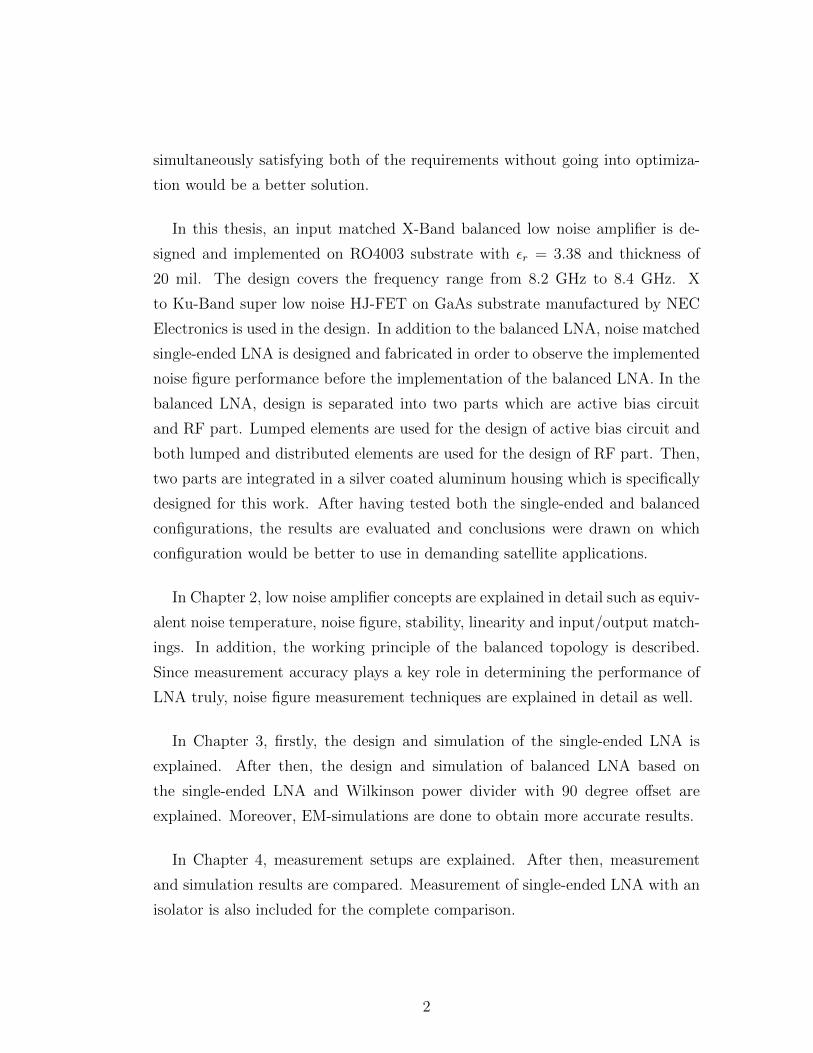
In this thesis, an input matched X-Band balanced low noise amplifier is de-
signed and implemented on RO4003 substrate with εr = 3.38 and thickness of
20 mil. The design covers the frequency range from 8.2 GHz to 8.4 GHz. X
to Ku-Band super low noise HJ-FET on GaAs substrate manufactured by NEC
Electronics is used in the design. In addition to the balanced LNA, noise matched
single-ended LNA is designed and fabricated in order to observe the implemented
noise figure performance before the implementation of the balanced LNA. In the
balanced LNA, design is separated into two parts which are active bias circuit
and RF part. Lumped elements are used for the design of active bias circuit and
both lumped and distributed elements are used for the design of RF part. Then,
two parts are integrated in a silver coated aluminum housing which is specifically
designed for this work. After having tested both the single-ended and balanced
configurations, the results are evaluated and conclusions were drawn on which
configuration would be better to use in demanding satellite applications.
In Chapter 2, low noise amplifier concepts are explained in detail such as equiv-
alent noise temperature, noise figure, stability, linearity and input/output match-
ings. In addition, the working principle of the balanced topology is described.
Since measurement accuracy plays a key role in determining the performance of
LNA truly, noise figure measurement techniques are explained in detail as well.
In Chapter 3, firstly, the design and simulation of the single-ended LNA is
explained. After then, the design and simulation of balanced LNA based on
the single-ended LNA and Wilkinson power divider with 90 degree offset are
explained. Moreover, EM-simulations are done to obtain more accurate results.
In Chapter 4, measurement setups are explained. After then, measurement
and simulation results are compared. Measurement of single-ended LNA with an
isolator is also included for the complete comparison.
2

Lastly, Chapter 5 concludes the thesis with a complete comparison of single-
ended, balanced and single-ended with an isolator low noise amplifiers in terms
of measured and simulated RF performances and cost.
3

Chapter 2
Background
2.1 Definition
Low noise amplifiers (LNAs) play a key role in receiver systems. Their main
function is to provide enough gain to minimize the noise of subsequent stages while
contributing a minimum amount of noise, thus preserving the required Signal-to-
Noise Ratio (SNR) of the system to extremely low power levels. In addition, an
LNA should be linear enough to handle large signals with minimal introduction
of distortion to eliminate in and out of channel interference. Lastly, LNA must
present a specific impedance, typically 50 Ω, to the input source especially when
a filter, duplexer, etc. precedes the LNA. Thus, the key parameters for an LNA
can be summarized as noise figure, gain, linearity and input matching.
4

2.2 Low Noise Amplifier Concepts
2.2.1 Equivalent Noise Temperature and Noise Figure
Amplifier noise power is the power measured at the output of an amplifier when
there is no input signal applied to it. Total output noise power consists of ampli-
fied input noise power and noise power generated internally by the amplifier. It
is possible to represent the added noise power by the amplifier as a noisy resistor
at the input and make the amplifier noiseless. In other words, a noisy resistor can
be used in modeling of noise power. This noise is known as thermal noise which
is caused by random motion of electrons in the resistor due to thermal agitation
[5, 6]. Available noise power of a resistor is given by
PN = kTB
where k is a Boltzman’s constant (1.38× 10⁻²³J/K), T is temperature in kelvins
and B is the noise bandwidth in cycles/sec which is generally the bandwidth of
device to be measured.
Equivalent noise temperature of a two-port device is defined as the increase
in the temperature of the source resistance required to account for all of the
noise contribution of the two-port device [8]. In other words, if a given noise
source produces an available power of PS watts in a bandwidth of B Hz, it can
be modeled as an equivalent thermal noise source characterized by an equivalent
noise temperature which is given by
Te =PS
kB
By using this definition, if the source resistor is at a physical temperature
of TS = 0K, a noisy two-port, an amplifier for instance, can be modeled by
a noiseless amplifier with an input resistor at an equivalent noise temperature
which is given by
Te =Pn
GAkB
5

where Pn is the noise power generated only by the amplifier itself.
Total output noise power is obtained by adding amplified input available noise
power to the noise power generated internally by the amplifier if they are uncor-
related. It can be expressed as follows:
PNo,total = GAPNi + Pn = GAkB(TS + Te)
where PNi is the input available noise power at a physical temperature of TS.
In addition to equivalent noise temperature, a noisy two-port can be character-
ized through the concept of noise figure whose definition is the ratio of the total
available noise power at the output to the output available noise power caused by
thermal noise coming only from the resistor at the standard room temperature
(To = 290K). Thus, noise figure can be written as
F =PNo,total
GAPNi
=GAPNi + Pn
GAPNi
= 1 +Pn
GAPNi
= 1 +TeTo
or
Te = (F − 1)To
Alternate definition of noise figure is a measure of the degradation between
available signal-to-noise power ratio at the input and available signal-to-noise
power ratio at the output, which is only valid when the input noise power, PNi,
is equal to kToB and it can be written as
F =SNRin
SNRout
=PSi/PNi
PSo/PNo
∣∣∣∣PNi=kToB
It can be questioned that why there is a reference temperature value for the
input noise source. The reason is simply found by assuming that there is no
noise at the input of a two-port network which means To = 0K, then input
signal-to-noise ratio is equal to infinity and output signal-to-noise ratio is a finite
number which means that noise figure definition does not give any reasonable
result. Therefore, there must be a reference temperature value for the input
6

noise source. In addition, it is interesting to note that the reason why 290K is
the reference temperature is simply that kT = 4.00× 10⁻²¹J , which is suggested
by Harald Friis[2].
In a typical microwave system, several stages are connected in cascade where
each stage degrades signal-to-noise ratio by adding noise. Cascaded noise figure
can be determined if the noise figure of each particular stage is known. For a
cascade of n stages, overall noise figure can be written as [1]:
Fcascade = F1 +F2 − 1
GA1
+F3 − 1
GA1GA2
+ · · ·+ Fn−1
GA1GA2 · · ·GAn−1
By using the definition given above, overall equivalent noise temperature for a
cascade of n stages can be written as
Te,cascade = Te,1 +Te,2GA1
+Te,3
GA1GA2
+ · · ·+ Te,nGA1GA2 · · ·GAn−1
2.2.2 Stability
Stability is defined as the ability of an amplifier to maintain effectiveness in its
nominal operating characteristics under different conditions [1]. If a negative
resistance condition occurs at the input or output, reflection coefficients becomes
|ΓIN | > 1
or
|ΓOUT | > 1
Having reflection coefficients greater than unity means that reflected power is
greater than the incident, therefore, instability, in other words, oscillation occurs.
In addition, stability is frequency-dependent means that an amplifier can act
as an oscillator for the out-of-band frequencies while maintaining its nominal
characteristics for the intended frequency band. Therefore, it can be concluded
that stability should be studied in detail.
Stability of an amplifier can be investigated either graphically using stability
circles on Smith Chart or analytically using a set of mathematical conditions. In
7

this work, to determine the degree of stability relative to other devices in addition
to unconditional stability, stability is investigated using single parameter test
criterion (µ-Parameter) with [1]:
µ =1− |S11|2
|S22 − S∗11∆|+ |S21S12|
and
∆ = S11S22 − S12S21
For unconditional stability, the following criteria must be satisfied:
µ > 1
To make an amplifier unconditionally stable, loss should be introduced. Since the
loss at the input significantly increases the noise figure of an amplifier, parallel
or series resistors should be placed at the output of an amplifier.
2.2.3 Linearity
1-dB compression point, P1dB, and third-order intercept point, IP3, are com-
monly used as linearity measures of an amplifier. 1-dB compression point is
defined as the power level where the gain drops by 1 dB. This point is usually
used to determine the linear output power level and it is more important for
power amplifier characterization rather than low noise amplifier characterization
[3]. In addition, 1-dB compression point is referred to either output or input.
Operating an amplifier under large-signal conditions causes distortion in the
output signal and this distortion causes new frequencies to appear at the output
signal. These new frequencies are called as harmonics for a single sinusoidal signal.
When input signal consists of two or more sinusoids, these new frequencies are
called as intermodulation products which are present along with harmonics. It
can be easily seen that all additional frequencies can be filtered out in narrow-
band amplifiers except the intermodulation products 2f1 − f2 and 2f2 − f1 due
to the fact that they are very close to the fundamental frequencies and hence fall
8
within the amplifier bandwidth. This effect is called third-order intermodulation
distortion. It is important to note that third-order intermodulation products are
significant for amplifiers because they set the upper limit on the dynamic range
[1].
The third-order intercept point which is used to calculate the levels of the
third order intermodulation products is defined as a hypothetical intercept point
where the first-order and third-order powers are equal [4]. This intercept point
is specified for either output or input.
2.2.4 Input and Output Matching
Since the first aim of LNA design is to obtain minimum noise figure, input match-
ing should be done accordingly. For an amplifier, there is an optimum source
impedance, Γopt, which leads to minimum noise figure. In order to obtain min-
imum noise figure, input impedance of an amplifier should be matched to this
optimum source impedance value. It is important to note that, however, optimum
source impedance that gives minimum noise figure is not necessarily the optimum
impedance for the maximum power transfer [2]. Therefore, one must sacrifice the
power gain, and therefore return loss, to obtain minimum noise figure, and vice
versa in order to optimize output signal-to-noise ratio unless those impedances
are same by coincidence.
In addition to obtain minimum noise figure, one of the other challenges in LNA
design is to obtain the maximum available gain. Therefore, conjugate matching
should be done at the output of the amplifier in order to get the best S/N at the
output of the system.
9
2.3 Balanced Amplifier
One of the commonly used techniques for obtaining large bandwidth and good
input and output VSWR is the balanced amplifier topology [7, 12]. It also pro-
vides better stability and higher linearity compared to single-ended amplifiers. It
consists of two identical amplifiers and two 90 hybrid couplers as shown in Figure
2.1. Firstly, the input power is split into two with a phase difference of 90. After
amplifier stage, amplified signals are recombined in phase by the output hybrid
coupler. For the reflected signals from the amplifiers, they are cancelled out at
the isolating resistor due to 180 phase difference between the branches caused
by the 90 offset line. Thus, input is matched to 50 ohm without any matching
network. This means that input matching network can be designed regardless of
the input return loss since it is already matched.
In this work, a 3 dB Wilkinson power divider with 90 offset line is used for
hybrid coupler but it should be known that it can be also realized by a 3 dB
Lange coupler or a 3 dB branch-line coupler.
Figure 2.1: Balanced amplifier configuration
In a single-ended amplifier, it is notably hard to achieve minimum noise figure
and minimum VSWR simultaneously as indicated in Section 2.2.4. Nonetheless,
minimum noise figure can be obtained without sacrificing VSWR by implement-
ing inductive source degeneration or balanced amplifier topology [15]. Inductive
source degeneration technique is more useful at low frequencies because it becomes
difficult to control the source inductance as frequency increases. Uncontrolled
10

source inductance can make the circuit unstable and lead oscillations [19]. How-
ever, it is possible to use this technique in MMIC applications at high frequencies
[16]. Thus, it is more reasonable to implement balanced amplifier topology when
discrete components are used. In the balanced topology, since reflected signals
from the amplifiers on each branch are cancelled at the termination port of the
coupler or the isolation resistor of the Wilkinson divider, the input matching of
the balanced amplifier depends only the input matching of the coupler [12]. Thus,
it provides the possible designing of the amplifier simultaneously for minimum
noise figure and minimum VSWR without compromise. If the couplers and am-
plifiers have similar characteristics and the loss of the couplers are ignored, noise
figure of the balanced amplifier is the same with the single-ended amplifier while
showing the matched load to the input [11]. Furthermore, it is also important
to note that balanced amplifiers are more stable compared to the single-ended
amplifiers because reflections are absorbed by the terminations of the couplers.
In addition, gain of the balanced amplifier is the same with the single-ended
amplifier except for the additional path losses if the gain of the each amplifier
is assumed to be the same. Moreover, it will still operate with 6 dB less gain
despite the fact that one of amplifiers fails. Another key thing to remember is
the fact that it becomes advantageous to use balanced amplifiers instead of the
single-ended amplifiers in terms of intermodulation and gain compression since
the signal power is shared equally between two branches and then recombined by
the output hybrid coupler in balanced amplifier topology therefore having 3 dB
higher OIP3 and P1dB values compared to the single-ended amplifiers [12].
All things considered, it seems reasonable to implement balanced amplifier
topology for the design of low noise amplifier if input reflection distortion and
redundancy are required parameters.
11
2.4 Simulation Techniques Used
In order to succeed in a complete LNA design with minimum iterations, advance
simulation techniques must be used. In this work, all simulations are made by
using Advance Design System (ADS) by Agilent.
Scattering parameters are used to characterize high frequency microwave com-
ponents. In other words, S-Parameters provide a complete description of the
network consisting of N-ports. All of the components, resistors, capacitors, tran-
sistors, etc., used in this work have S-Parameters which are provided by their
manufacturers in *.s2p file format. S-Parameter file of the transistor also in-
cludes the noise parameters which enable the noise calculations.
2.5 Noise Figure Measurement Techniques
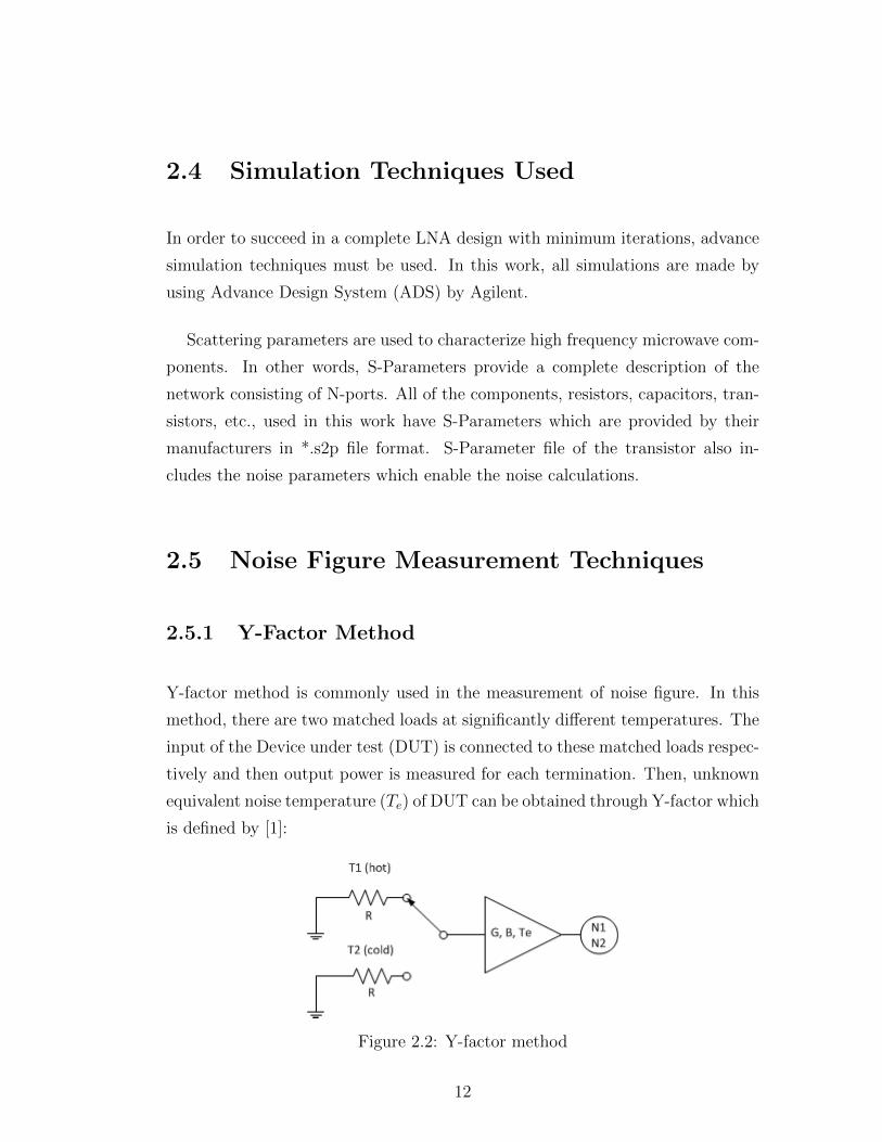
2.5.1 Y-Factor Method
Y-factor method is commonly used in the measurement of noise figure. In this
method, there are two matched loads at significantly different temperatures. The
input of the Device under test (DUT) is connected to these matched loads respec-
tively and then output power is measured for each termination. Then, unknown
equivalent noise temperature (Te) of DUT can be obtained through Y-factor which
is defined by [1]:
Figure 2.2: Y-factor method
12

Y =PNo,1
PNo,2
where
PNo,1 = GAkB(T1 + Te)
PNo,2 = GAkB(T2 + Te)
Thus,
Y =T1 + TeT2 + Te
Te =T1 − Y T2Y − 1
It is important to note that two matched terminations must be at significantly
different temperatures; otherwise, inaccurate results will be obtained. These
different temperature are usually obtained from active noise source which provides
specific noise power in a particular frequency range and they are characterized
by their excess noise ratio (ENR) values versus frequency. ENR is defined as:
ENR = 10log10
(TN − ToTo
)
where TN is the equivalent noise temperature of the noise source in hot state
and To is the equivalent noise temperature of a passive source at room temperature
(290K) in cold state.
Note that the definition of ENR assumes that the equivalent noise tempera-
ture of a noise source in cold state is always 290K. However, equivalent noise
temperature in cold state may be hotter or colder than 290K and in that case
ENR value will not be correct and this leads to en error in noise figure because
ENR values are always referenced to 290K. The physical temperature of the
cold noise source should then be measured and the equivalent noise temperature
of a noise source in cold state should be corrected. Temperature correction is
mostly done by noise figure instruments [9].
13
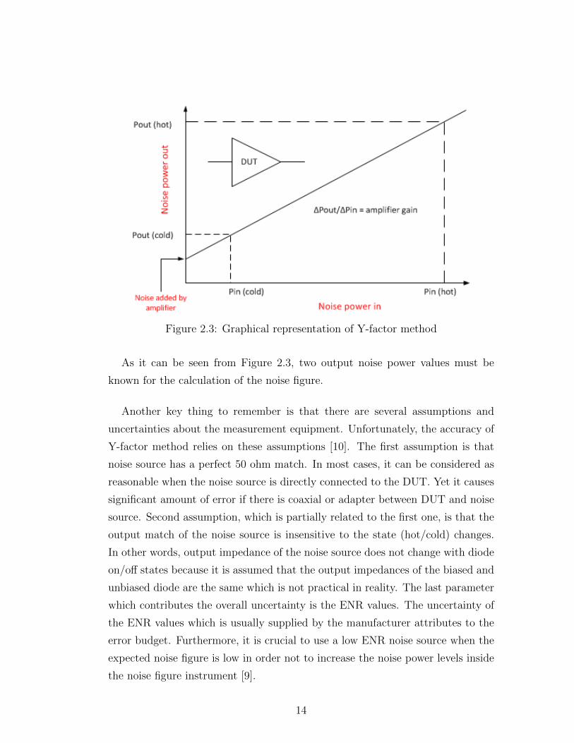
Figure 2.3: Graphical representation of Y-factor method
As it can be seen from Figure 2.3, two output noise power values must be
known for the calculation of the noise figure.
Another key thing to remember is that there are several assumptions and
uncertainties about the measurement equipment. Unfortunately, the accuracy of
Y-factor method relies on these assumptions [10]. The first assumption is that
noise source has a perfect 50 ohm match. In most cases, it can be considered as
reasonable when the noise source is directly connected to the DUT. Yet it causes
significant amount of error if there is coaxial or adapter between DUT and noise
source. Second assumption, which is partially related to the first one, is that the
output match of the noise source is insensitive to the state (hot/cold) changes.
In other words, output impedance of the noise source does not change with diode
on/off states because it is assumed that the output impedances of the biased and
unbiased diode are the same which is not practical in reality. The last parameter
which contributes the overall uncertainty is the ENR values. The uncertainty of
the ENR values which is usually supplied by the manufacturer attributes to the
error budget. Furthermore, it is crucial to use a low ENR noise source when the
expected noise figure is low in order not to increase the noise power levels inside
the noise figure instrument [9].
14

2.5.2 Cold Source Method
Instead of using two matched loads at significantly different temperatures, a single
matched load at room temperature, which is the reason why the method is called
as cold source, is used for the output noise power measurement. This output
noise consists of the amplified input noise and the noise generated internally
by the amplifier. If the gain of the DUT is accurately known, then the noise
generated by the amplifier can be easily calculated. Vector network analyzer
(VNA) is used for making the gain measurement with a high degree of precision.
As it can be seen from the Figure 2.4, a single output power measurement is
enough for the calculation of noise figure thanks to known DUT gain in contrast
to the Figure 2.3.
Figure 2.4: Graphical representation of cold-source method
Cold-source method presents a more accurate measurement compared to the
Y-factor since it does not have the uncertainties that Y-factor method has but
still it has some uncertainties such as the S-parameter uncertainty and the 50-
ohm termination at the input of the DUT on which the error magnitude greatly
depends. Although cold-source method has its own uncertainties, it has lower
measurement uncertainty (0.2 dB) than the Y-factor method (0.5 dB) [10].
15

Chapter 3
Design and Simulation
3.1 Transistor Selection
Since noise parameters of a transistor plays a key role in the noise figure of a com-
plete amplifier, transistor selection is an important step in laying the foundation
of the design of low noise amplifier. In this work, N-channel HJ-FET NE3511S02
manufactured by NEC Electronics is used. It has a minimum noise figure of 0.26
dB and associated gain of 13 dB at 8.3 GHz when the drain voltage is 2 V and
drain current is 10 mA.
In this work, a single-ended low noise amplifier is designed and simulated in
ADS. As a second step, a balanced topology is implemented using the designed
single-ended amplifier.
16
3.2 Single-Ended Low Noise Amplifier Design
3.2.1 Active Bias Circuit
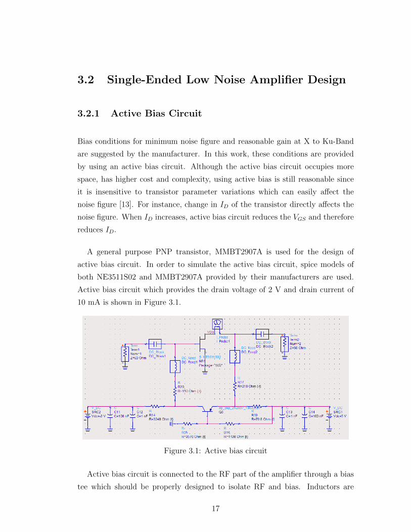
Bias conditions for minimum noise figure and reasonable gain at X to Ku-Band
are suggested by the manufacturer. In this work, these conditions are provided
by using an active bias circuit. Although the active bias circuit occupies more
space, has higher cost and complexity, using active bias is still reasonable since
it is insensitive to transistor parameter variations which can easily affect the
noise figure [13]. For instance, change in ID of the transistor directly affects the
noise figure. When ID increases, active bias circuit reduces the VGS and therefore
reduces ID.
A general purpose PNP transistor, MMBT2907A is used for the design of
active bias circuit. In order to simulate the active bias circuit, spice models of
both NE3511S02 and MMBT2907A provided by their manufacturers are used.
Active bias circuit which provides the drain voltage of 2 V and drain current of
10 mA is shown in Figure 3.1.
Figure 3.1: Active bias circuit
Active bias circuit is connected to the RF part of the amplifier through a bias
tee which should be properly designed to isolate RF and bias. Inductors are
17

commonly used as RF-choke. Their self-resonance frequency should be higher
than the frequency of operation. Otherwise, they may act like a capacitor rather
than an inductor. For this reason, high impedance λ/4 length transmission lines
are generally used as RF-chokes at high frequencies rather than lumped elements.
A shorted λ/4 length transmission line acts as an open circuit at the frequency
of operation. Another benefit of using shorted λ/4 length tranmission line is that
they also short out the second harmonic. Furthermore, radial stubs are also used
to improve isolation.
Figure 3.2: Bias tee
3.2.2 Stability
In order to stabilize the circuit unconditionally, µ-parameter method is used in
a wide frequency range. From this point on, all simulations except active bias
are done with the S-parameters of the transistor because using measured data is
more reliable. The simulated µ-parameter for the circuit given in Figure 3.1 is
shown in Figure 3.3. As it can be shown from the figure, circuit is conditionally
stable before stabilization.
18

Figure 3.3: µ-parameter before stabilization
Usually a series resistor is used for stabilization. It is important to note that,
however, resistor causes the loss in the circuit which significantly degrades the
noise figure. Therefore, it must be placed after the transistor and a capacitor
must be placed in parallel with it so that the capacitor shorts out the resistor at
the frequency of operation. In addition, S-parameters of these components are
used in the simulation for more reliable results. Schematics of the circuit after
stabilization is given in Figure 3.4. The simulated µ-parameter for this circuit
is shown in Figure 3.5. It can be concluded that the circuit is unconditionally
stable.
19

Figure 3.4: Schematics of the circuit after stabilization
20

Figure 3.5: µ-parameter after stabilization
3.2.3 Input Matching Network
Input matching determines the noise figure, gain and input return loss of the
amplifier. Since our goal is to achieve minimum noise figure which can be obtained
from the transistor, the input impedance of the transistor should be matched to
the optimum source impedance for the minimum noise figure which is provided
by the manufacturer. As a result of noise matching that is regardless of input
return loss, gain will be reduced.
S-parameter simulations are done for the design of input matching. The sim-
ulation results of unmatched circuit is shown in Figure 3.6. Red circles are the
noise circles with 0.1 dB step and blue circles are the gain circles with 1 dB step.
As it can be seen from the figure, the optimum source impedance for minimum
noise figure and the impedance for maximum power transfer (conjugate match-
ing) is far away from each other. Note that the impedance for maximum power
transfer is obtained by using available gain circles.
21

Figure 3.6: Noise and gain circles before input matching
Distributed elements are used for matching networks because lumped elements
may degrade the RF performance at high frequencies. Moreover, using distributed
elements simplifies the circuit implementation since they do not require soldering.
Hence, input matching is realized by a series transmission line followed by an open
stub shown in Figure 3.7. After the realization of the input matching, the source
impedance is shown in Figure 3.8. As it can be seen from the figure, source
impedance is matched to the optimum impedance for the minimum noise figure.
22

Figure 3.7: Input matching network
Figure 3.8: Noise and gain circles after input matching
23
3.2.4 Output Matching Network
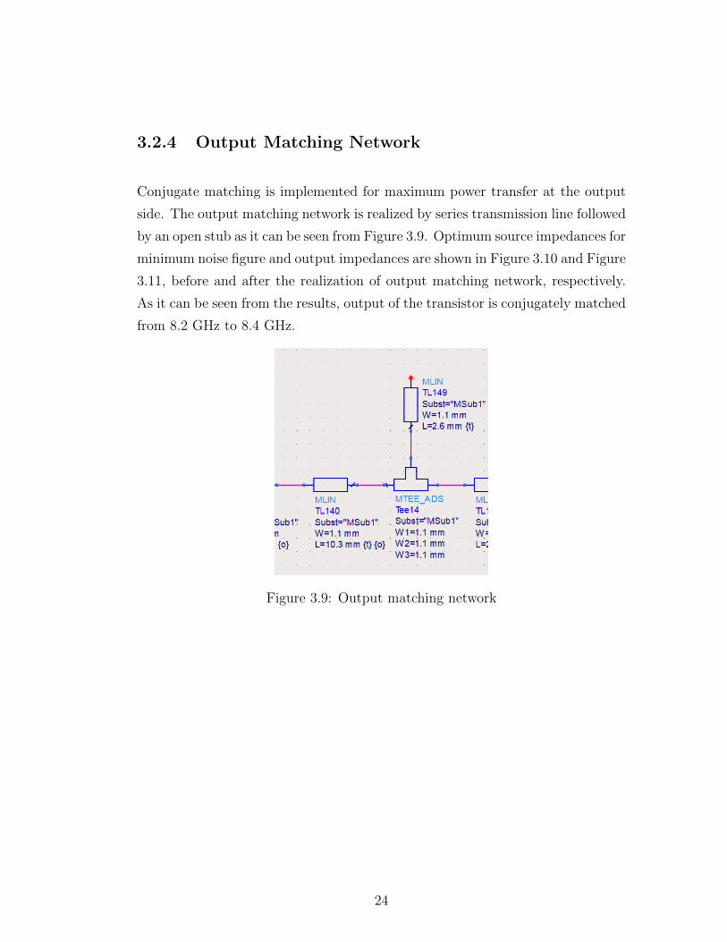
Conjugate matching is implemented for maximum power transfer at the output
side. The output matching network is realized by series transmission line followed
by an open stub as it can be seen from Figure 3.9. Optimum source impedances for
minimum noise figure and output impedances are shown in Figure 3.10 and Figure
3.11, before and after the realization of output matching network, respectively.
As it can be seen from the results, output of the transistor is conjugately matched
from 8.2 GHz to 8.4 GHz.
Figure 3.9: Output matching network
24
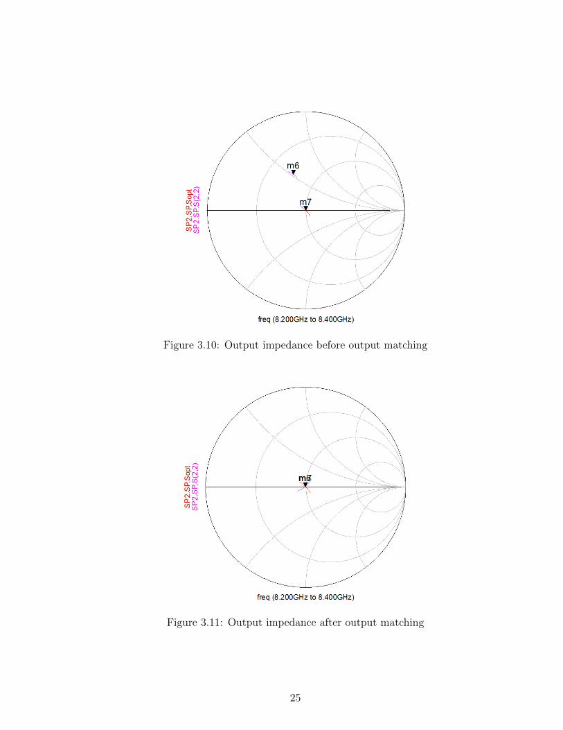
Figure 3.10: Output impedance before output matching
Figure 3.11: Output impedance after output matching
25

3.2.5 Final Design and Layout
Single-ended low noise amplifier is designed with linear simulations in ADS. In
order to improve design performance and increase confidence, Momentum, which
is a 3D planar electromagnetic (EM) simulator of ADS, is used for passive cir-
cuit modelling and analysis in the design. It uses frequency-domain Method of
Moments (MoM) technology to accurately simulate complex EM effects including
couplings and parasitics. Thus, the more accurate results can be obtained.
After some tuning and optimization in Momentum, design is completed and
the final schematics including Momentum EM-model is shown in Figure 3.12.
Stability, S-parameter and noise figure simulation results of this circuit are shown
in Figure 3.13, 3.14 and 3.15, respectively. As it can be seen from the results,
complete circuit is unconditionally stable while having a maximum noise figure
of 0.54 dB, a minimum gain of 13.8 and a minimum input return loss of 5.7 dB.
PCB is also designed in Momentum. Rogers 4003 with 20 mil thickness is used.
Final layout of the design is shown in figure 3.16. Note that thin lines with small
gaps are added to the each open stub for tuning during real-time measurements.
26

Figure 3.12: Complete schematics of the circuit including Momentum layout
27
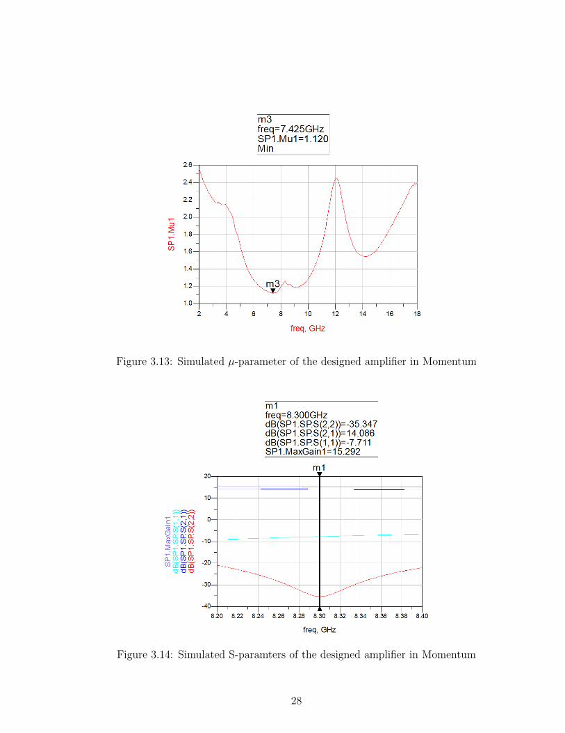
Figure 3.13: Simulated µ-parameter of the designed amplifier in Momentum
Figure 3.14: Simulated S-paramters of the designed amplifier in Momentum
28

Figure 3.15: Simulated noise figure of the designed amplifier in Momentum
Figure 3.16: Final layout of the single-ended low noise amplifier
29

3.3 Balanced Low Noise Amplifier Design
3.3.1 Active Bias Circuit
Active bias circuit and bias tee designed for the single-ended design are used in
the balanced amplifier because bias conditions of the transistors are same.
3.3.2 Stability
Since the designed single-ended circuit is already stable, there is no need to add
more resistors for stabilizing the circuits in the balanced design. Thus, same
stability resistors and capacitor are used for the balanced design.
3.3.3 Input Matching Network
In order to achieve minimum noise figure which can be obtained from the transis-
tor, input impedance of the transistor should be matched to the optimum source
impedance which is provided by the manufacturer. Since this matching is done for
the single-ended design, there is no need to re-design it. Same matching network
is used for the transistors on each branch.
3.3.4 Output Matching Network
Output matching network for the single-ended design is used in the balanced
design as well because conjugate matching should be done for maximum power
transfer.
30
3.3.5 Wilkinson Power Divider/Combiner
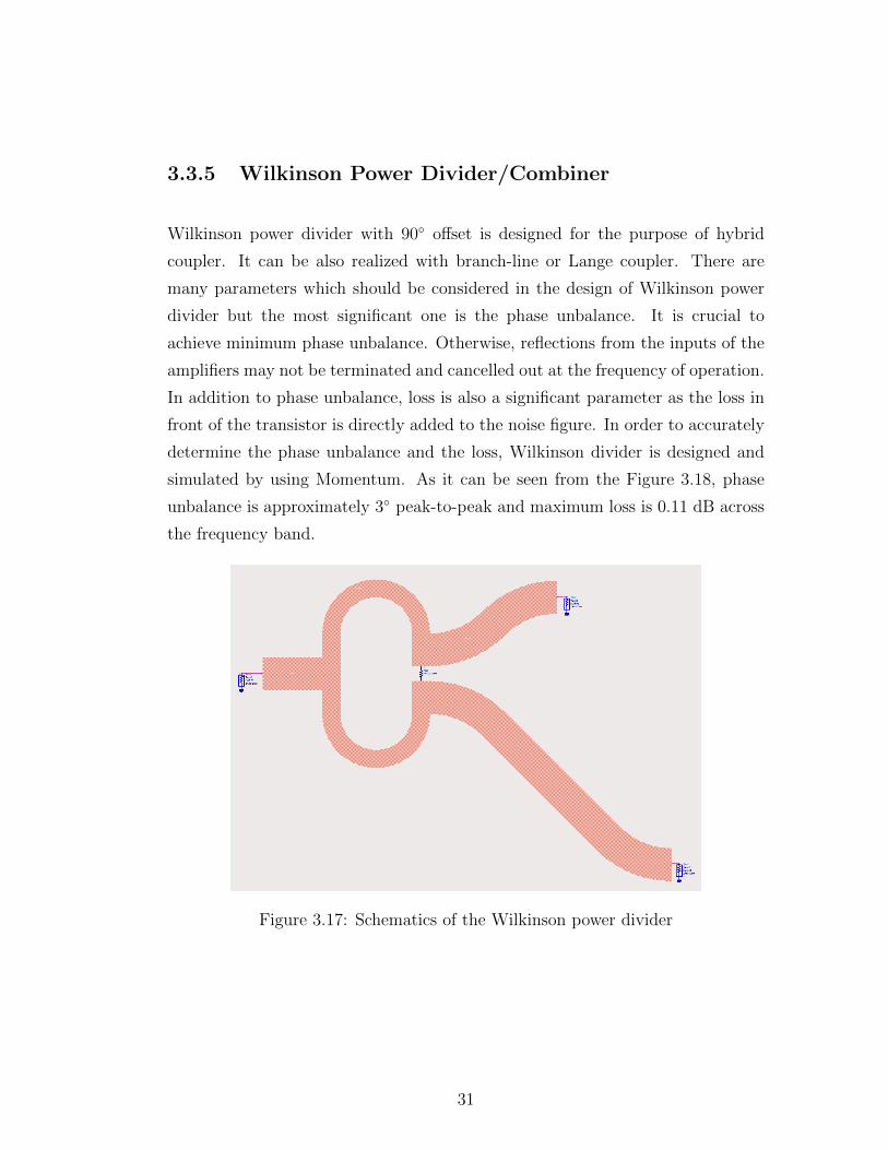
Wilkinson power divider with 90 offset is designed for the purpose of hybrid
coupler. It can be also realized with branch-line or Lange coupler. There are
many parameters which should be considered in the design of Wilkinson power
divider but the most significant one is the phase unbalance. It is crucial to
achieve minimum phase unbalance. Otherwise, reflections from the inputs of the
amplifiers may not be terminated and cancelled out at the frequency of operation.
In addition to phase unbalance, loss is also a significant parameter as the loss in
front of the transistor is directly added to the noise figure. In order to accurately
determine the phase unbalance and the loss, Wilkinson divider is designed and
simulated by using Momentum. As it can be seen from the Figure 3.18, phase
unbalance is approximately 3 peak-to-peak and maximum loss is 0.11 dB across
the frequency band.
Figure 3.17: Schematics of the Wilkinson power divider
31

(a) Phase difference of the two arms
(b) Loss of the two arms
Figure 3.18: Simulation results of Wilkinson power divider
32
3.3.6 Final Design and Layout
After some tuning and optimization in Momentum, the design is completed and
the final schematics of the balanced low noise amplifier including Momentum
EM-model is shown in Figure 3.19. Input and output impedances and optimum
impedance value for minimum noise figure of this circuit are shown on the Smith
chart given in Figure 3.20. All of them are located at the center of the Smith
chart. In addition, stability, S-parameter and noise figure simulation results of
this circuit is shown in Figure 3.21, 3.22 and 3.23, respectively.
As it can be seen from the results, complete circuit is unconditionally stable
while having a maximum noise figure of 0.63 dB, a minimum gain of 13.8 dB
and a minimum input return loss of 31.2 dB. Note that gain is approximately the
same with single-ended design. However, noise figure is increased by 0.1 dB due
to the contribution of path loss caused by Wilkinson power divider. This small
increment can be considered as the cost of obtaining low VSWR values in the
design of low noise amplifiers with balanced topology.
PCB design is done by using Momentum. Rogers 4003 with 20 mil thickness
is used as in the single-ended design. Final layout of the design is shown in figure
3.24. Note that thin lines with small gaps are added to the each open stub for
tuning during real-time measurements as in the single-ended design. As it can be
seen from Figure 3.24, active bias circuit is not included as in single-ended LNA.
In balanced LNA, RF and bias circuits are separated for easy debugging. Final
layout of active bias circuit is given in Figure 3.25.
33

Figure 3.19: Schematics of the final design of the balanced low noise amplifier
34

Figure 3.20: Input and output impedances of the balanced low noise amplifier
Figure 3.21: Simulated µ-parameter of the balanced low noise amplifier designed
in Momentum
35

Figure 3.22: Simulated S-parameters of the balanced low noise amplifier designed
in Momentum
Figure 3.23: Simulated noise figure of the balanced low noise amplifier designed
in Momentum
36
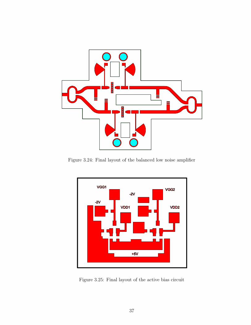
Figure 3.24: Final layout of the balanced low noise amplifier
Figure 3.25: Final layout of the active bias circuit
37

Chapter 4
Measurements
4.1 Measurement Preparations and Setups
Firstly, single-ended LNA is mounted on the PCB and tested. After then, the
balanced LNA is mounted on the PCB and then assembled as shown in Figure 4.1.
In order to complete the design and implementation of an amplifier, metal hous-
ing must be provided to prevent possible interference and oscillations and avoid
bending of thin PCB. Unusual shape of the PCB of balanced amplifier, which can
be seen from Figure 3.24, is caused by the internal walls of the metal housing.
These walls are placed intentionally and the cavity dimensions are minimized to
avoid box resonances as much as possible.
38
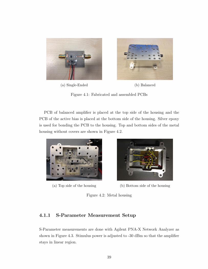
(a) Single-Ended (b) Balanced
Figure 4.1: Fabricated and assembled PCBs
PCB of balanced amplifier is placed at the top side of the housing and the
PCB of the active bias is placed at the bottom side of the housing. Silver epoxy
is used for bonding the PCB to the housing. Top and bottom sides of the metal
housing without covers are shown in Figure 4.2.
(a) Top side of the housing (b) Bottom side of the housing
Figure 4.2: Metal housing
4.1.1 S-Parameter Measurement Setup
S-Parameter measurements are done with Agilent PNA-X Network Analyzer as
shown in Figure 4.3. Stimulus power is adjusted to -30 dBm so that the amplifier
stays in linear region.
39
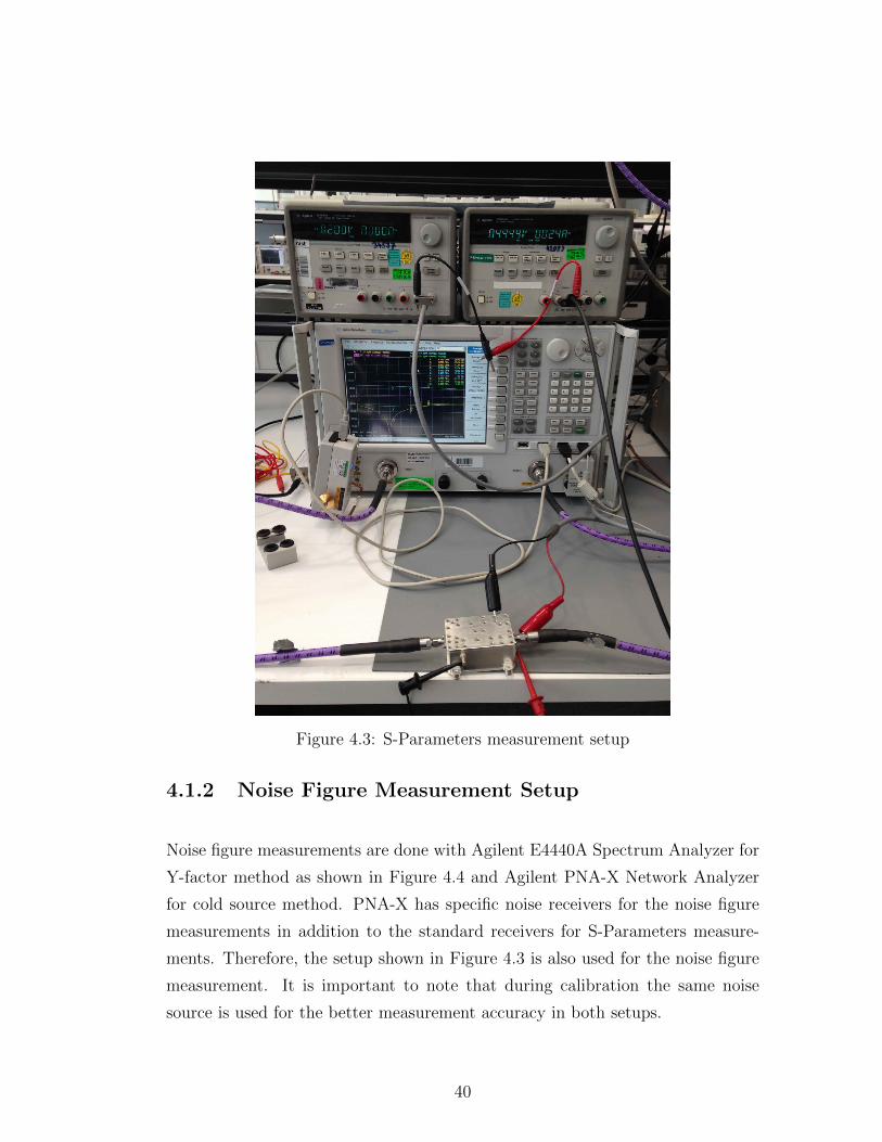
Figure 4.3: S-Parameters measurement setup
4.1.2 Noise Figure Measurement Setup
Noise figure measurements are done with Agilent E4440A Spectrum Analyzer for
Y-factor method as shown in Figure 4.4 and Agilent PNA-X Network Analyzer
for cold source method. PNA-X has specific noise receivers for the noise figure
measurements in addition to the standard receivers for S-Parameters measure-
ments. Therefore, the setup shown in Figure 4.3 is also used for the noise figure
measurement. It is important to note that during calibration the same noise
source is used for the better measurement accuracy in both setups.
40
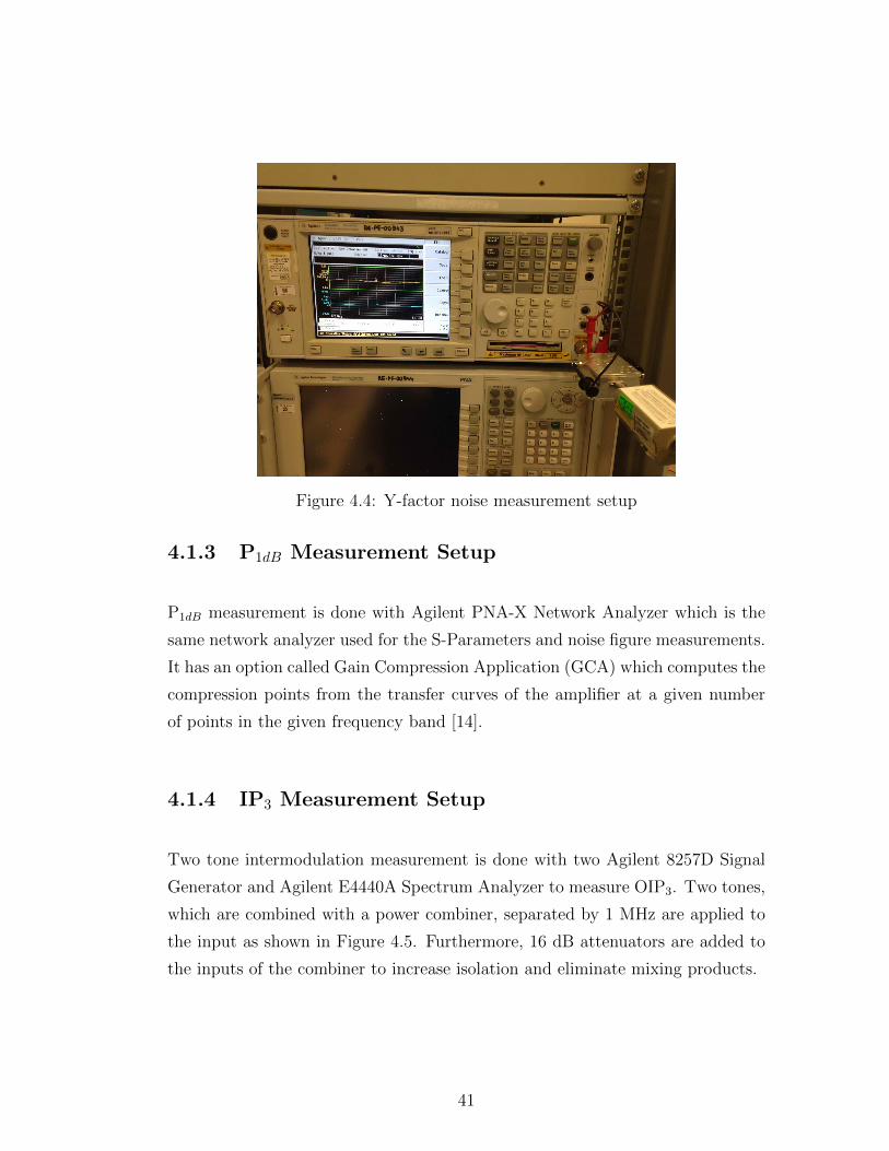
Figure 4.4: Y-factor noise measurement setup
4.1.3 P1dB Measurement Setup
P1dB measurement is done with Agilent PNA-X Network Analyzer which is the
same network analyzer used for the S-Parameters and noise figure measurements.
It has an option called Gain Compression Application (GCA) which computes the
compression points from the transfer curves of the amplifier at a given number
of points in the given frequency band [14].
4.1.4 IP3 Measurement Setup
Two tone intermodulation measurement is done with two Agilent 8257D Signal
Generator and Agilent E4440A Spectrum Analyzer to measure OIP3. Two tones,
which are combined with a power combiner, separated by 1 MHz are applied to
the input as shown in Figure 4.5. Furthermore, 16 dB attenuators are added to
the inputs of the combiner to increase isolation and eliminate mixing products.
41
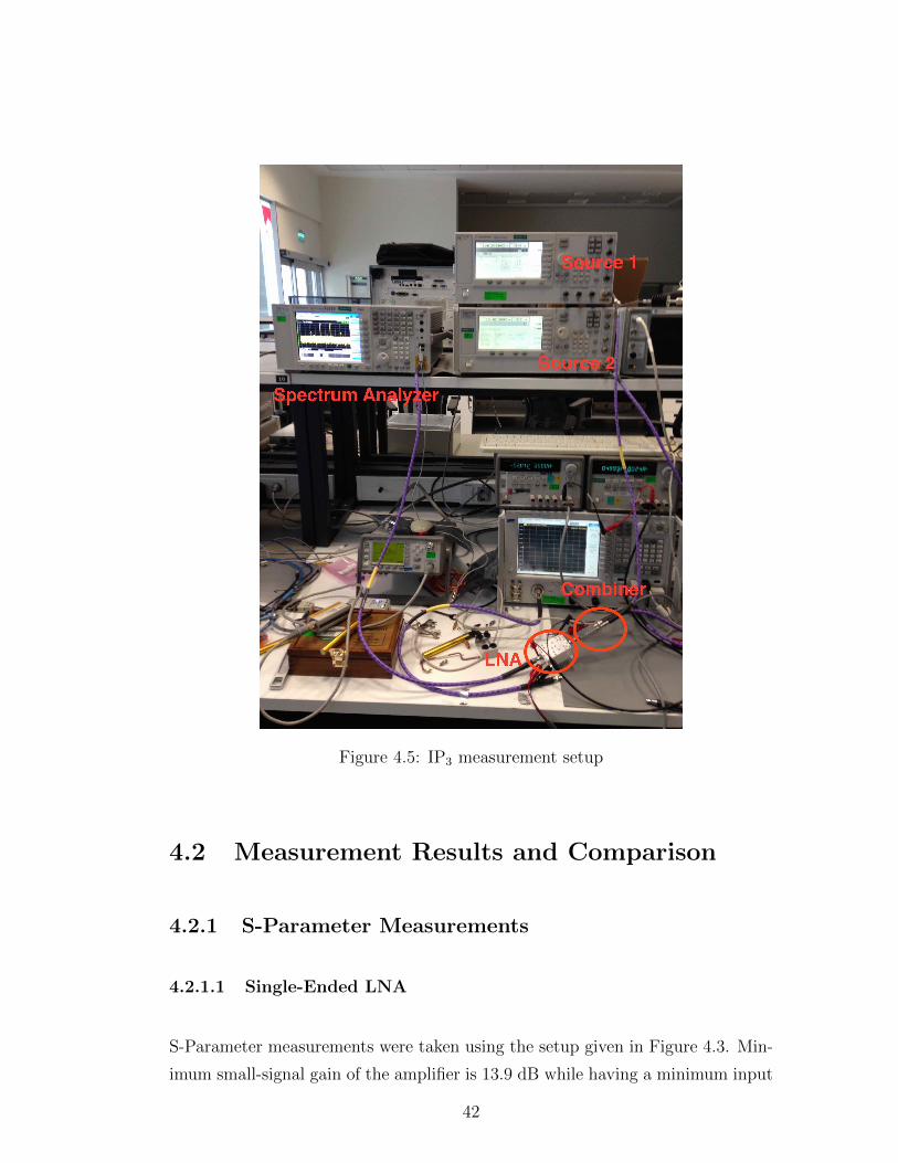
Figure 4.5: IP3 measurement setup
4.2 Measurement Results and Comparison
4.2.1 S-Parameter Measurements
4.2.1.1 Single-Ended LNA
S-Parameter measurements were taken using the setup given in Figure 4.3. Min-
imum small-signal gain of the amplifier is 13.9 dB while having a minimum input
42
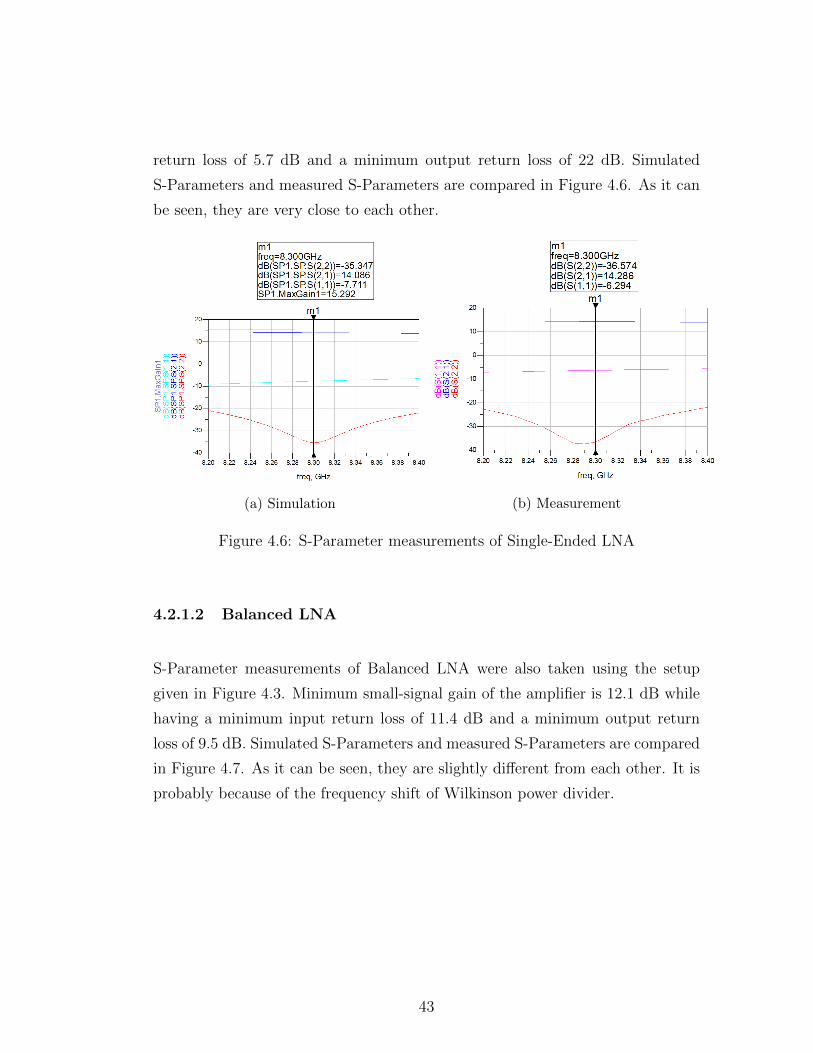
return loss of 5.7 dB and a minimum output return loss of 22 dB. Simulated
S-Parameters and measured S-Parameters are compared in Figure 4.6. As it can
be seen, they are very close to each other.
(a) Simulation (b) Measurement
Figure 4.6: S-Parameter measurements of Single-Ended LNA
4.2.1.2 Balanced LNA
S-Parameter measurements of Balanced LNA were also taken using the setup
given in Figure 4.3. Minimum small-signal gain of the amplifier is 12.1 dB while
having a minimum input return loss of 11.4 dB and a minimum output return
loss of 9.5 dB. Simulated S-Parameters and measured S-Parameters are compared
in Figure 4.7. As it can be seen, they are slightly different from each other. It is
probably because of the frequency shift of Wilkinson power divider.
43

(a) Simulation (b) Measurement
Figure 4.7: S-Parameter measurements of Balanced LNA
4.2.2 Y-Factor Noise Figure Measurements
4.2.2.1 Single-Ended LNA
Measurement was taken using the setup given in Figure 4.4. Simulated and
measured values are compared in Figure 4.8. Maximum measured noise figure is
1.4 dB which is different than simulated value. One of the reasons behind this
difference is the input connector because its loss is directly added to the total
noise figure.
44

(a) Simulation
(b) Measurement
Figure 4.8: Y-factor noise figure measurement of Single-Ended LNA
45
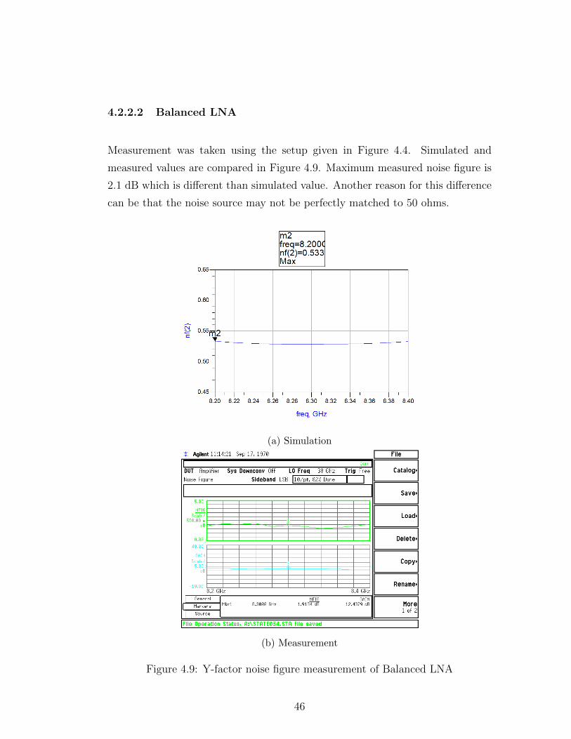
4.2.2.2 Balanced LNA
Measurement was taken using the setup given in Figure 4.4. Simulated and
measured values are compared in Figure 4.9. Maximum measured noise figure is
2.1 dB which is different than simulated value. Another reason for this difference
can be that the noise source may not be perfectly matched to 50 ohms.
(a) Simulation
(b) Measurement
Figure 4.9: Y-factor noise figure measurement of Balanced LNA
46
4.2.3 Cold Source Noise Figure Measurements
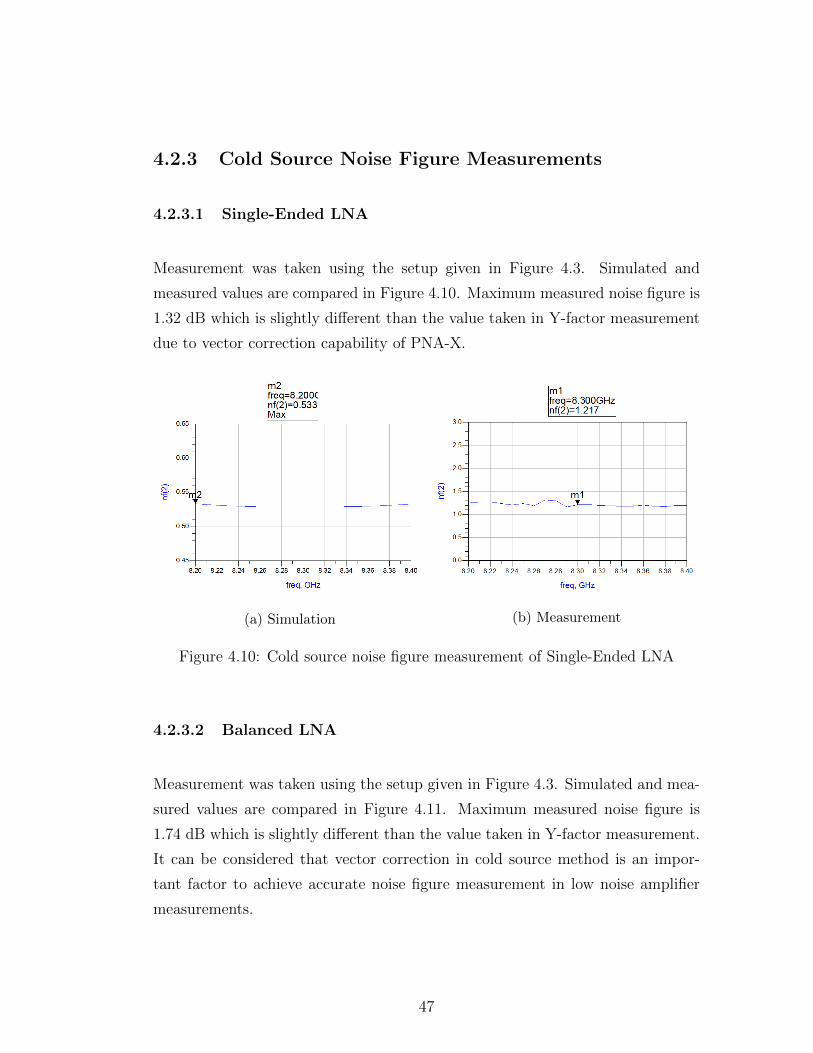
4.2.3.1 Single-Ended LNA
Measurement was taken using the setup given in Figure 4.3. Simulated and
measured values are compared in Figure 4.10. Maximum measured noise figure is
1.32 dB which is slightly different than the value taken in Y-factor measurement
due to vector correction capability of PNA-X.
(a) Simulation (b) Measurement
Figure 4.10: Cold source noise figure measurement of Single-Ended LNA
4.2.3.2 Balanced LNA
Measurement was taken using the setup given in Figure 4.3. Simulated and mea-
sured values are compared in Figure 4.11. Maximum measured noise figure is
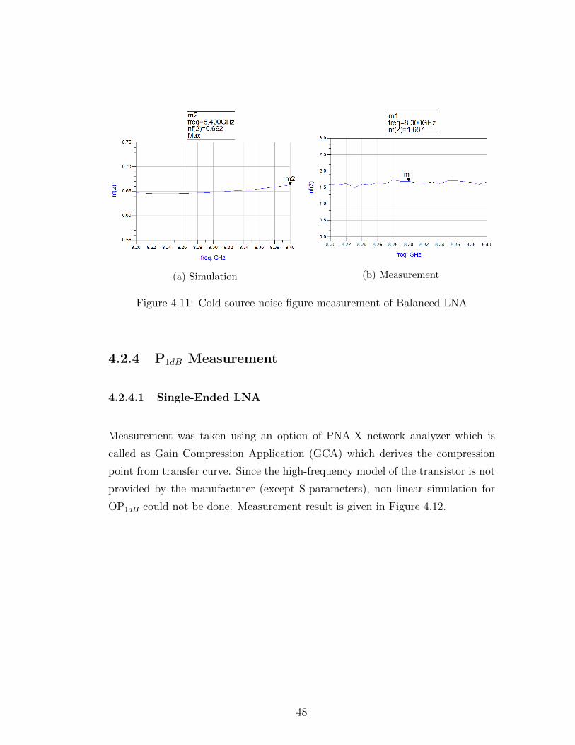
1.74 dB which is slightly different than the value taken in Y-factor measurement.
It can be considered that vector correction in cold source method is an impor-
tant factor to achieve accurate noise figure measurement in low noise amplifier
measurements.
47
(a) Simulation (b) Measurement
Figure 4.11: Cold source noise figure measurement of Balanced LNA
4.2.4 P1dB Measurement
4.2.4.1 Single-Ended LNA
Measurement was taken using an option of PNA-X network analyzer which is
called as Gain Compression Application (GCA) which derives the compression
point from transfer curve. Since the high-frequency model of the transistor is not
provided by the manufacturer (except S-parameters), non-linear simulation for
OP1dB could not be done. Measurement result is given in Figure 4.12.
48
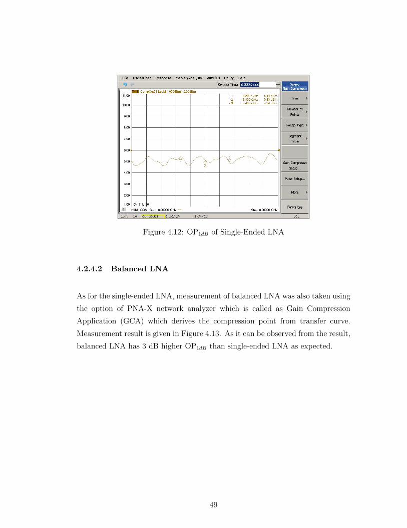
Figure 4.12: OP1dB of Single-Ended LNA
4.2.4.2 Balanced LNA
As for the single-ended LNA, measurement of balanced LNA was also taken using
the option of PNA-X network analyzer which is called as Gain Compression
Application (GCA) which derives the compression point from transfer curve.
Measurement result is given in Figure 4.13. As it can be observed from the result,
balanced LNA has 3 dB higher OP1dB than single-ended LNA as expected.
49

Figure 4.13: OP1dB of Balanced LNA
4.2.5 IP3 Measurement
4.2.5.1 Single-Ended LNA
Measurement was taken using the setup shown in Figure 4.5 and the result is
shown in Figure 4.14. Calculated OIP3 is 18.7 dBm which is approximately 10-15
dB higher than the measured P1dB of single-ended LNA as expected.
50

Figure 4.14: Two tone intermodulation test of Single-Ended LNA
4.2.5.2 Balanced LNA
Measurement was taken using the setup shown in Figure 4.5 and the result is
shown in Figure 4.15. Calculated OIP3 is 21.5 dBm which is approximately 10-15
dB higher than the measured P1dB of single-ended LNA as expected. As it can
be observed from the results, balanced LNA has approximately 3 dB higher OIP3
than single-ended LNA as expected.
51
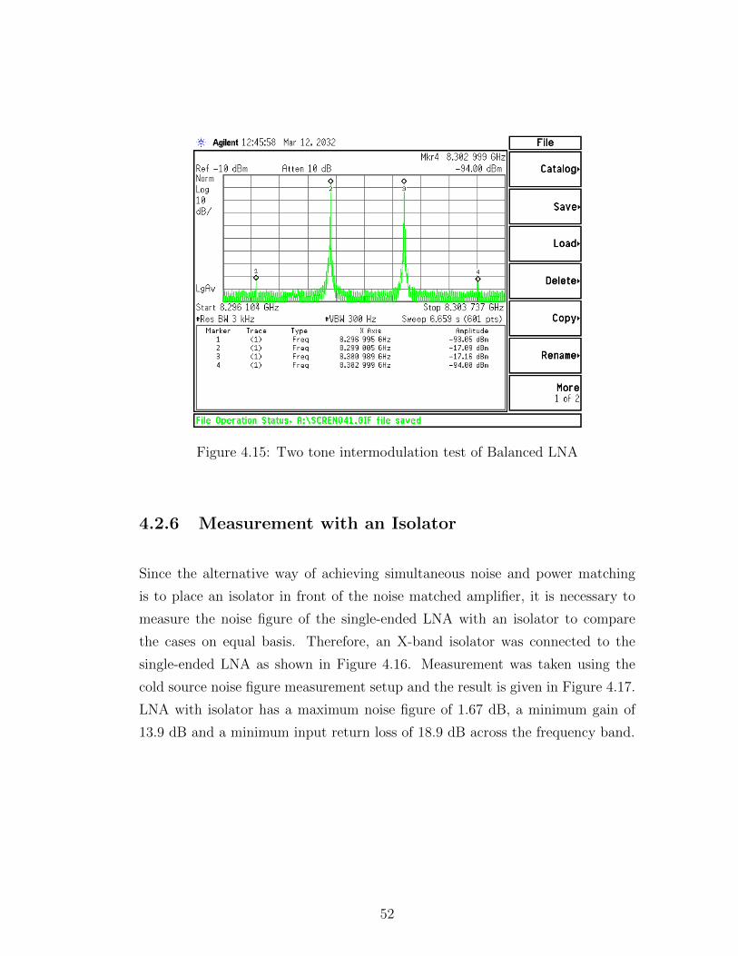
Figure 4.15: Two tone intermodulation test of Balanced LNA
4.2.6 Measurement with an Isolator
Since the alternative way of achieving simultaneous noise and power matching
is to place an isolator in front of the noise matched amplifier, it is necessary to
measure the noise figure of the single-ended LNA with an isolator to compare
the cases on equal basis. Therefore, an X-band isolator was connected to the
single-ended LNA as shown in Figure 4.16. Measurement was taken using the
cold source noise figure measurement setup and the result is given in Figure 4.17.
LNA with isolator has a maximum noise figure of 1.67 dB, a minimum gain of
13.9 dB and a minimum input return loss of 18.9 dB across the frequency band.
52

Figure 4.16: Single-Ended LNA with an X-band isolator
(a) S-Parameter measurement results(b) Cold source noise figure measurement
result
Figure 4.17: Measurement results of Single-Ended LNA with isolator
53

4.2.7 Summary
Table 1, Table 2 and Table 3 shows the summary of single-ended LNA, balanced
LNA and single-ended LNA with isolator, respectively. The best and worst values
are given along the frequency band.
Specification Simulated Value Measured Value
Frequency Band 8200 MHz - 8400 MHz 8200 MHz - 8400 MHz
Noise Figure 0.53 dB - 0.54 dB 1.16 dB - 1.32 dB
Gain 14.3 dB - 13.8 dB 14.6 dB - 13.9 dB
Input Return Loss 9.1 dB - 5.7 dB 7.2 dB - 5.7 dB
Output Return Loss 35.4 dB - 29 dB 37.5 dB - 22 dB
Table 4.1: Summary of the Single-Ended LNA
Specification Simulated Value Measured Value
Frequency Band 8200 MHz - 8400 MHz 8200 MHz - 8400 MHz
Noise Figure 0.62 dB - 0.63 dB 1.5 dB - 1.74 dB
Gain 14.3 dB - 13.8 dB 13.5 dB - 12.1 dB
Input Return Loss 44 dB - 31.2 dB 28.1 dB - 11.4 dB
Output Return Loss 44 dB - 31 dB 12.3 dB - 9.5 dB
Table 4.2: Summary of the Balanced LNA
Specification Measured Value
Frequency Band 8200 MHz - 8400 MHz
Noise Figure 1.54 dB - 1.67 dB
Gain 14.4 dB - 13.9 dB
Input Return Loss 20 dB - 18.9 dB
Output Return Loss 25.2 dB - 18.6 dB
Table 4.3: Summary of the Single-Ended LNA with isolator
54
Chapter 5
Conclusion
In this work, design and implementation of an input matched X-band low noise
amplifier was studied, constructed and measured. Input matching is an important
parameter if a filter precedes the LNA. Poor matching results in excessive loss in
the filter, which degrades the overall system performance. These input filters are
usually designed so that the output termination impedance of the filter is 50 ohms
and they are very sensitive to the changes in the output termination impedances,
which makes the input matching critical [17]. However, input matching becomes
insignificant if there is no input filter in the receiver architecture. Another key
work in the design of LNA is to optimize Signal-to-Noise Ratio (SNR). Since
the transmitter power cannot be increased indefinitely, the only way to increase
SNR is to provide sufficient gain to minimize the noise of subsequent stages while
contributing a minimum amount of noise by the input stage. Therefore, there
should be a lower limit for the gain, for instance 10 dB, to avoid the excessive
noise contribution from the subsequent stages.
To accomplish the goals mentioned above, several techniques from the litera-
ture were investigated and balanced amplifier topology was chosen to work on.
Balanced topology provides matched input and output impedances due to the
fact that reflected signals from the output of the coupler are cancelled at the ter-
mination port of the coupler. Thereby, it is possible to design matching networks
55

regardless of the input/output return losses. Thus, the input of the LNA is di-
rectly matched to the optimum source impedance for minimum noise figure while
maintaining matched load to the input source. For the output of the LNA, max-
imum power transfer matching is done. In addition to the balanced LNA, noise
matched single-ended LNA is designed and fabricated in order to observe the
implemented noise figure performance before the implementation of the balanced
LNA.
The designed single-ended amplifier produced a maximum noise figure of 0.54
dB and a minimum input return loss of 5.7 dB during the simulations. The
fabricated single-ended amplifier has a maximum noise figure of 1.32 dB and a
minimum input return loss of 5.7 dB. Input connector, fabrication tolerances,
lot-to-lot variations and in the lot variations of the transistor in terms of noise
properties can be considered as the possible reasons for the difference between
the simulation and measurement results.
After successfully implementing the single-ended LNA, the balanced LNA was
designed and fabricated. Moreover, aluminum housing for the balanced LNA
was designed and fabricated to prevent possible interferences and avoid bending
of the thing PCB. The main goal in the design of the housing is to prevent box
resonance without absorber by minimizing the internal dimensions of the housing.
Furthermore, RF and active bias circuits are separated so that they are placed
back-to-back on the central plate of the housing. The designed amplifier produced
a minimum noise figure of 0.65 dB and a minimum input return loss of 26.5 dB
during the simulations. The assembled balanced amplifier has a maximum noise
figure of 1.74 dB and a minimum input return loss of 11.4 dB. Measured noise
figure value is slightly higher than the simulated one. One of the reasons for this
difference can be attributed to the possible gain difference between the branches
which results in an increased noise figure [18]. In addition, mismatch in the
coupler can be considered as one of the reasons for an increased noise figure
because phase difference at the center frequency is no longer 90 degrees. During
measurements, it is observed that box resonance occurs when the cover of the
housing is screwed tightly. Therefore, absorber is attached to the cover to avoid
the box resonance. It can be easily observed that frequency shift is occurred in
56

the fabricated balanced LNA in spite of the fact that single-ended LNA does not
have a such frequency shift. This fact indicates that the Wilkinson power divider
might be causing the frequency shift.
Lastly, noise figure and gain measurements of the single-ended LNA were re-
peated with an X-band isolator for a comparison on equal basis. The measured
maximum noise figure is 1.67 dB and minimum input return loss is 18.9 dB. The
results are quite similar with the results of balanced LNA when it is assumed that
the frequency shift is corrected. Thus, cost should be considered as a parameter
for the choice of which one will be used since the RF performances are similar.
In that case, the balanced amplifier would be better to use because isolator costs
much higher than a couple of transistors, resistors and capacitors.
For the future work, noise figure of the balanced amplifier can be reduced by
minimizing the loss between the input connector and the gate of the transistor.
Moreover, frequency shift which is a result of the mismatch in the coupler can be
corrected.
57
Bibliography
[1] M.M. Radmanesh, Radio Frequency and Microwave Electronics Illustrated.
Prentice Hall PTR, 2001.
[2] T.H. Lee, The Design of CMOS Radio-Frequency Integrated Circuits. Cam-
bridge University Press, 2nd Edition, 1998.
[3] S. C. Cripps, RF Power AMplifiers for Wireless Communications. Artech
House, 2006.
[4] D. M. Pozar, Microwave Engineering. Addison-Wesley Publishing Company,
1990.
[5] H. Nyquist, ”Thermal Agitation of Electrical Charges in Conductors”, Phys.
Rev.. v. 32, July 1928. pp. 110-13.
[6] I. J. Bahl, Fundamentals of RF and Microwave Transistor Amplifiers. John
Wiley & Sons, Inc., 2009.
[7] G. Gonzalez, Microwave Transistor Amplifiers Analysis and Design. Prentice
Hall PTR, 2nd Edition, 1996.
[8] T. Reyhan, ”Noise”, Telecommunication Electronics Lecture Notes, 2004.
[9] Agilent Technologies, ”Noise Figure Measurement Accuracy - The Y-Factor
Method.”
[10] Agilent Technologies, ”High Accuracy Noise Figure Measurements Using
PNA-X Series Network Analyzer.”
58

[11] K. Kurokawa, ”Design Theory of Balanced Transistor Amplifiers”, Bell Sys-
tem Technical Journal, vol. 44, pp. 1675 - 1698, October 1965.
[12] R. S. Engelbrecht and K. Kurokawa, ”A Wideband Low Noise L-band Bal-
anced Transistor Amplifier”, Proc. IEEE, vol. 53, p. 237, 1965.
[13] S. Long, ”Bias Circuit Design for Microwave Amplifiers”, Communication
Electronics Course Notes, 2007.
[14] Agilent Technologies, ”Gain Compression Application for Amplifier Test.”
[15] J. Engberg, ”Simultaneous Input Power Match and Noise Optimization Us-
ing Feedback”, Proc. 4th European Microwave Conference, Oct 1974, pp.
385-389.
[16] R. E. Lehmann and D. D. Heston, ”X-Band Monolithic Series Feedback
LNA”, IEEE Transactions on Microwave Theory and Techniques, vol. MTT-
33, no. 12, December 1985.
[17] D. K. Shaeffer and T. H. Lee, ”A 1.5-V, 1.5-GHz CMOS Low Noise Ampli-
fier”, IEEE Journal of Solid-State Circuits, vol. 32, no. 5, May 1997.
[18] S. Guoying and B. Jingfu, ”Analysis and Simulation of Balanced Low Noise
Amplifier”, IEEE Circuits and Systems International Conference on Testing
and Diagnosis (ICTD), pp. 1-4, April 2009.
[19] Avago Technologies, ”A Low Current, High Intercept Point, Low Noise Am-
plifier for 1900 MHz using the Avago ATF-38143 Low Noise PHEMT.”
59