an overview of designing analog interface with tm320f28xx
TRANSCRIPT

SPRAAP6A – May 2008 Submit Documentation Feedback
An Overview of Designing Analog Interface With TMS320F28xx/28xxx DSCs 1
Pradeep Shinde
Application Report SPRAAP6A – May 2008
An Overview of Designing Analog Interface With TMS320F28xx/28xxx DSCs
ABSTRACT
This application report provides guidelines that take you through everything from configuring the ADC and related registers correctly, responding to interrupts, and board design recommendations; this may be particularly useful for first-time users of the TMS320C2000™ digital signal processor (DSP) platform devices and for firmware engineers with less exposure to the analog world. Various system consideration issues are discussed, such as setting sampling rate, proper sequencing of input channels for efficient transfer of digital counts to the system’s data memory, inputting the driver/filter circuit, and power supply and calibration. Information from various documents was compiled to form a handy guide for those designing with the onboard analog-to-digital converter (ADC) that is available on the TMS320F28xx/28xxx generation of digital signal controllers (DSCs). The associated code demonstrates this implementation using an F280x eZdsp™ board. It can be used as a software framework for a new design which uses this ADC extensively. Project collateral and source code discussed in this application report can be downloaded from the following URL: http://www.ti.com/lit/zip/SPRAAP6.
Contents 1 Introduction ........................................................................................... 2 2 Architecture and Description of ADC Module ....................................... 3 3 ADC Set-Up and Operation .................................................................. 4 4 DMA and Calibration Functionality in F2823x and F2833x Families ................................ 12 5 Schematic and Board Design ............................................................. 16 6 ADC Calibration .................................................................................. 18 7 Additional Support .............................................................................. 18 8 References ......................................................................................... 19 Appendix A F280xx and F281x Differences ............................................................................. 20
List of Figures 1 Simplified Block Diagram of ADC Module ............................................ 3 2 ADC Pin Connections for TMS320F280xx ........................................... 5 3 Analog Input Impedance Model (F280xx) ............................................. 5 4 Typical Buffer/Driver Circuit for ADCIN ................................................. 6 5 ADC Clock Chain .................................................................................. 8 6 Sequential Mode Timing and Sample Rates ........................................ 9 7 ADC Interrupts Multiplexed via PIE Block ........................................... 11 8 Simplified Hardware State Machine Flow ........................................... 14 9 Address Control .................................................................................. 14 10 Layout Example 1: Component Placement ........................................ 17 11 Layout Example 2: Routing/Traces ..................................................... 17 12 ADC Conversion Transfer Function .................................................... 18
List of Tables
2 An Overview of Designing Analog Interface With TMS320F28xx/28xxx DSCs SPRAAP6A – May 2008 Submit Documentation Feedback
Introduction www.ti.com
A-1 F280xx and F281x Peripheral Differences ....................................................................... 20 1 Introduction
The TMS320F28x DSC’s 16-channel,12-bit ADC peripheral enables designer to interface analog signals directly with the processor, as required for various embedded control applications. The enhanced ADC peripheral included on the TMS320F28xx DSCs has 12 bits of resolution and can achieve a speed of up to 12.5 millions of samples per second (MSPS) (6.25 MSPS and 3.75 MSPS for some parts) through a pipeline architecture that makes it useful in many applications requiring the monitoring of analog signals (see Figure 1). Additional features, such as a 16-channel multiplexer, auto-sequencer, dual sample-and-hold (S/H) circuits, and multiple interrupt schemes, make it quite flexible for use in embedded control and data logging applications. The ADC needs to be configured properly to take full advantage of the flexibility of this peripheral. This detailed approach is achieved through various circuit blocks that need to be understood and set up appropriately. Understanding and setting up the required sampling rate, aligning the channels using auto-sequencers, and an interrupt configuration to read the results to accomplish optimum performance. A scenario using the DSP/BIOS™ software kernel foundation (TI’s Real Time Operating System for TMS320™ DSPs) is covered in this document. This document also discusses major guidelines for board design issues and the system-level design considerations. The ADC peripheral on the TMS320F281x, TMS320F280xx, TMS320F2804x and newer TMS320F2832x generations have almost an identical architecture. The specifications for these peripherals differ for a few parameters on the F280xx and F281x generations; these differences are described in Appendix A. This application report uses information from the F280xx devices to walk-through the setup using different diagrams. The associated code is also directed toward the F280xx devices, but can be easily modified for the F281x devices. For more detailed specifications, see Understanding Data Converters (SLAA013) [1] and TMS320F2809, TMS320F2808, TMS320F2806, TMS320F2802, TMS320F2801, TMS320C2802, TMS320C2801, and TMS320F2801x DSPs Data Manual (SPRS230) [2]. For more set-up information and register details, see the TMS320x280x, 2801x, 2804x Analog-to-Digital Converter (ADC) Reference Guide (SPRU716) [4], TMS320x2833x Analog-to-Digital Converter (ADC) Module (SPRU812) [18] and the TMS320x281x DSP Analog-to-Digital Converter (ADC) Reference Guide (SPRU060) [5]. For more detailed information regarding system control and interrupt references, see the Buffer Op Amp to ADC Circuit Collection (SLOA098) [6]. If you are unfamiliar with ADC parameters and terminology, see Understanding Data Converters (SLAA013) [1].
TMS320C2000, DSP/BIOS, TMS320, TMS320C28x are trademarks of Texas Instruments. eZdsp is a trademark of Spectrum Digital, Inc. All other trademarks are the property of their respective owners.
SPRAAP6A – May 2008 Submit Documentation Feedback
An Overview of Designing Analog Interface With TMS320F28xx/28xxx DSCs 3
Ch Set (CONV15)
ADCRESULT0
Ch Set (CONV03) Ch Set (CONV11)
www.ti.com Architecture and Description of ADC Module
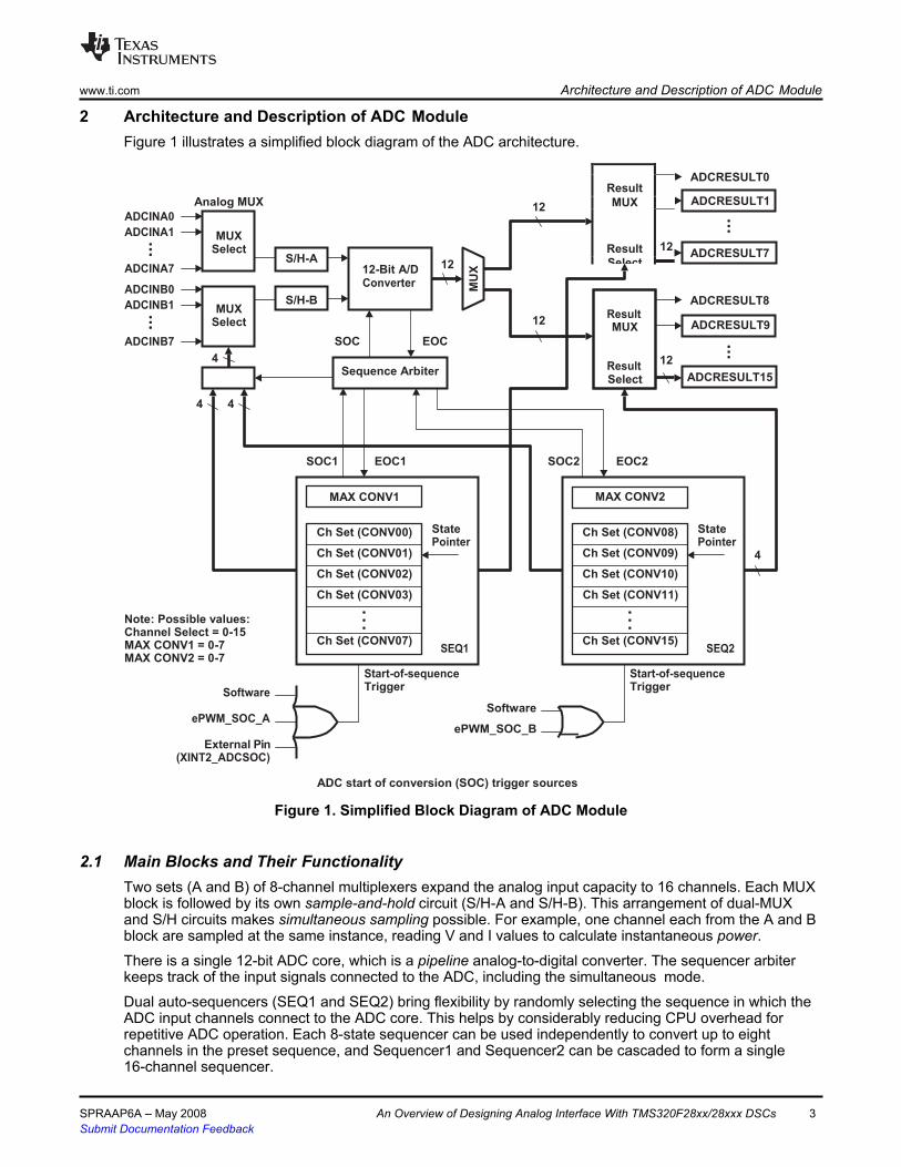
2 Architecture and Description of ADC Module Figure 1 illustrates a simplified block diagram of the ADC architecture.
ADCINA0 ADCINA1
ADCINA7 ADCINB0 ADCINB1
ADCINB7
Analog MUX
4
12
12
12
SOC EOC 12
Sequence Arbiter
4 4
SOC1 EOC1 SOC2 EOC2
MAX CONV2
State Pointer
State Pointer
4
Note: Possible values: Channel Select = 0-15 MAX CONV1 = 0-7 MAX CONV2 = 0-7
SEQ1 SEQ2
Software
ePWM_SOC_A
External Pin (XINT2_ADCSOC)
Start-of-sequence Trigger
Software ePWM_SOC_B
Start-of-sequence Trigger
ADC start of conversion (SOC) trigger sources
Figure 1. Simplified Block Diagram of ADC Module
2.1 Main Blocks and Their Functionality
Two sets (A and B) of 8-channel multiplexers expand the analog input capacity to 16 channels. Each MUX block is followed by its own sample-and-hold circuit (S/H-A and S/H-B). This arrangement of dual-MUX and S/H circuits makes simultaneous sampling possible. For example, one channel each from the A and B block are sampled at the same instance, reading V and I values to calculate instantaneous power. There is a single 12-bit ADC core, which is a pipeline analog-to-digital converter. The sequencer arbiter keeps track of the input signals connected to the ADC, including the simultaneous mode. Dual auto-sequencers (SEQ1 and SEQ2) bring flexibility by randomly selecting the sequence in which the ADC input channels connect to the ADC core. This helps by considerably reducing CPU overhead for repetitive ADC operation. Each 8-state sequencer can be used independently to convert up to eight channels in the preset sequence, and Sequencer1 and Sequencer2 can be cascaded to form a single 16-channel sequencer.
Ch Set (CONV10) Ch Set (CONV02)
ADCRESULT8 S/H-B
ADCRESULT1
MUX
Select
Ch Set (CONV09) Ch Set (CONV08)
Ch Set (CONV07)
Ch Set (CONV01) Ch Set (CONV00)
ADCRESULT9
Result MUX
Result Select
12-Bit A/D Converter
S/H-A
MUX
Select
MAX CONV1
ADCRESULT15
ADCRESULT7
MU
X
Result MUX
Result 12 Select
4 An Overview of Designing Analog Interface With TMS320F28xx/28xxx DSCs SPRAAP6A – May 2008 Submit Documentation Feedback
ADC Set-Up and Operation www.ti.com
You can set the number of conversions per sequence (up to eight for each sequencer, used individually or up to 16, if cascaded), using the ADCMAXCONV register. Figure 1 shows that one out of four different signals can be used as a start-of-conversion (SOC) trigger for Sequencer 1 (SEQ1), and either software or the pulse-width modulation (PWM) trigger can be used for Sequencer 2 (SEQ2). There are 16 Result Registers (ADCRESULT0 – ADCRESULT15) that hold the ADC count before they are transferred to system memory. Any input channel (ADCINxx) can be assigned for each conversion within the sequencer. This facilitates repeating or skipping any channel and the sequence in which channel numbers are assigned for the ADCRESULTn registers. The end of sequence (EOS) generates three different interrupt signals ADCINT, SEQ1INT and SEQ2INT, which can be used to transfer the readings from the result registers to the system memory. The interrupt service routine (ISR) for this interrupt is the only CPU intervention for the ADC operations. This flexible arrangement reduces CPU overhead while the complete conversion activity goes on in the background. For more detailed information on the autoconversion sequencer, see the TMS320x280x, 2801x, 2804x DSP Analog-to-Digital Converter(ADC) Reference Guide (SPRU716) [4] and the TMS320x281x DSP Analog-to-Digital Converter (ADC) Reference Guide (SPRU060) [5].
2.2 Key Specifications Review the specifications before going into the set-up information; it is assumed that you are familiar with data converter terminologies. Key specifications to consider at this stage are sampling rate and input analog range. Gain and offset errors are the next important parameters, as they should meet the effective resolution that is acceptable for the system. • Maximum sampling rate is 12.5/6.25/3.75 MSPS for the F280x/F280xx devices and 12.5 MSPS for the
F281x devices. • Maximum ADC clock is 25/12.5/6.25 MHz for F280x/F2801x devices and 25 MHz for F281x devices. • Range of input analog signal is 0 V to 3.0 V, and like all ADCs, offset error and gain error are present. For more detailed information regarding the values of other specifications, see the Electrical Specifications sections of TMS320F2809, TMS320F2808, TMS320F2806, TMS320F2802, TMS320F2801, TMS320C2802, TMS320C2801, and TMS320F2801x DSPs Data Manual (SPRS230) [2], TMS320F2810, TMS320F2811, TMS320F2812, TMS320C2810, TMS320C2811,TMS320C2812 Digital Signal Processors Data Manual (SPRS174) [3] and TMS320F28335, TMS320F28334, TMS320F28332, TMS320F28235, TMS320F28234, TMS320F28232 Digital Signal Controllers (DSCs) Data Manual (SPRS439) [19].
3 ADC Set-Up and Operation
This section discusses design issues. On the hardware side, the important consideration is the external passive parts that are added for proper functionality. It is also important to understand how the incoming analog signals are connected to the ADCIN pins to achieve specified performance. Power supply and the external voltage reference circuits are discussed in Section 3.2.2.
3.1 Hardware Setup There are two main aspects of the hardware design for this ADC: • Passive components that are added for proper functioning of ADC • Circuitry to process incoming analog signals. Section 5 contains more tips on complete schematic and
board design.
SPRAAP6A – May 2008 Submit Documentation Feedback
An Overview of Designing Analog Interface With TMS320F28xx/28xxx DSCs 5
ADC Set-Up and Operation www.ti.com
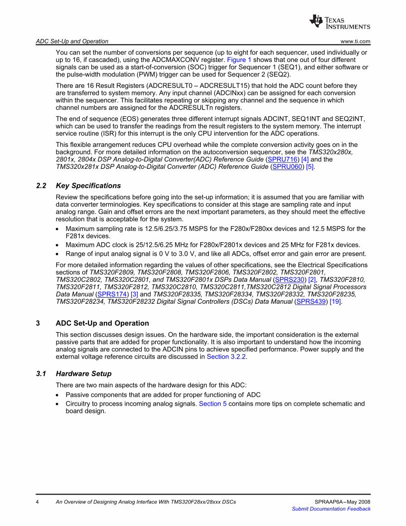
3.1.1 Required External Components for the ADC Few external components are required for biasing of internal band gap reference and filtering noise on reference voltage signals. Figure 2, reproduced from F280xx data sheets, shows these parts and their connections.
ADC 16-Channel Analog Inputs
ADC External Current Bias Resistor
ADC Reference Positive Output
ADCINA[7:0] ADCINB[7:0]
ADCLO ADCREFIN
ADCRESEXT
ADCREFP
Analog Input 0 V to 3 V with respect to ADCLO
Connect to analog ground Float or ground if internal reference is used
22 KΘ
2.2 µF(A) ADCREFP and ADCREFM
ADC Reference Medium Output
ADC Power
ADC Analog and Reference I/O Power
ADCREFM
VDD1A18
VDD2A18
VSS1AGND
VSS2AGND
VDDA2
VSSA2
VDDAIO
VSSAIO
2.2 µF(A) should not be loaded by external circuitry
ADC Analog Power Pin (1.8 V) ADC Analog Power Pin (1.8 V) ADC Analog Ground Pin ADC Analog Ground Pin
ADC Analog Power Pin (3.3 V) ADC Analog Ground Pin ADC Analog Power Pin (3.3 V) ADC Analog I/O Ground Pin
Figure 2. ADC Pin Connections for TMS320F280xx
These pins must be connected as shown above. The F281x devices require different values for these parts (Appendix A).
3.1.2 Analog Input Signal Interface
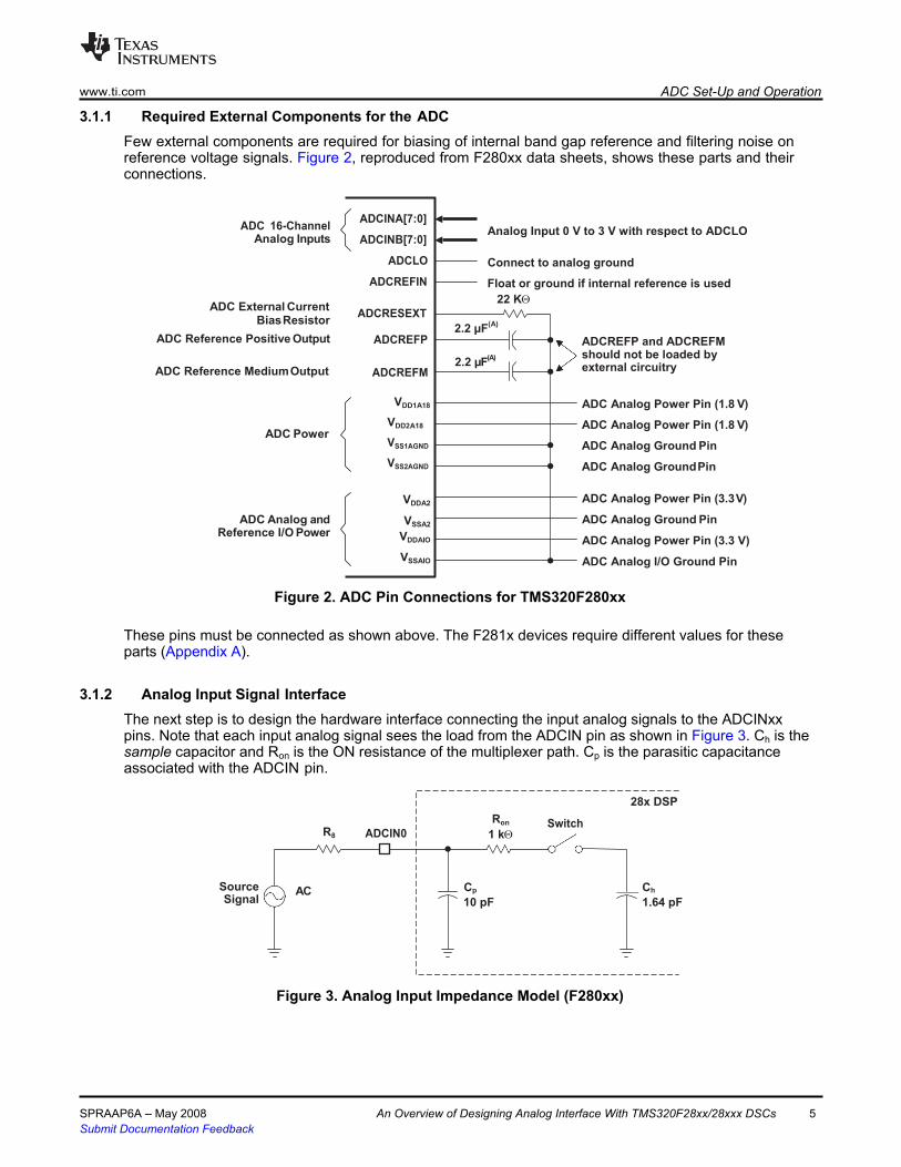
The next step is to design the hardware interface connecting the input analog signals to the ADCINxx pins. Note that each input analog signal sees the load from the ADCIN pin as shown in Figure 3. Ch is the sample capacitor and Ron is the ON resistance of the multiplexer path. Cp is the parasitic capacitance associated with the ADCIN pin.
R8 ADCIN0
Ron
1 kΘ
Switch
28x DSP
Source AC Signal Cp 10 pF
Ch 1.64 pF
Figure 3. Analog Input Impedance Model (F280xx)
6 An Overview of Designing Analog Interface With TMS320F28xx/28xxx DSCs SPRAAP6A – May 2008 Submit Documentation Feedback
ADC Set-Up and Operation www.ti.com
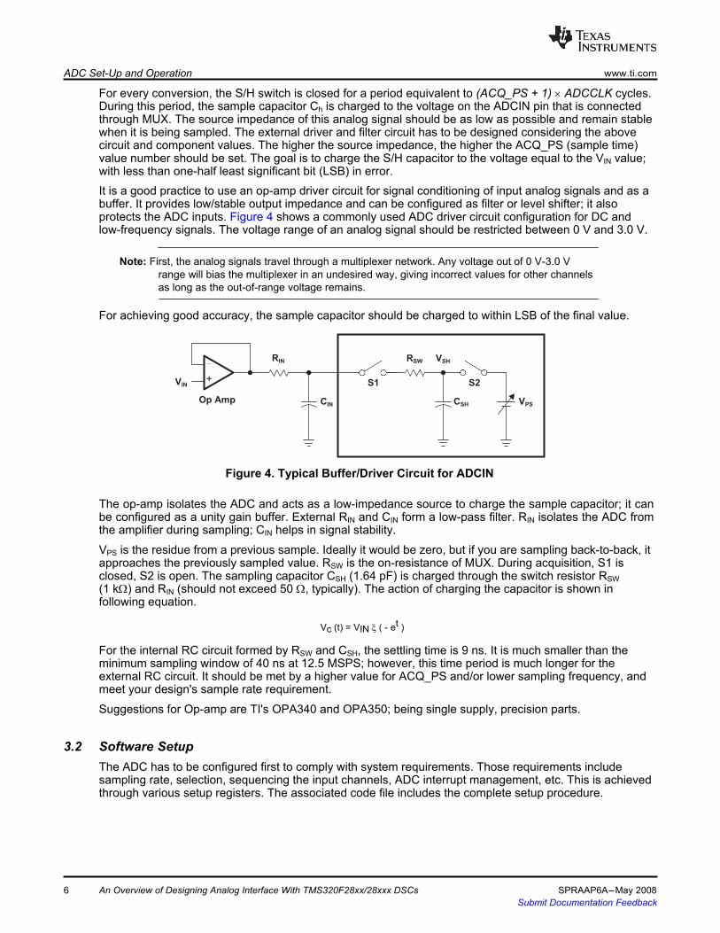
For every conversion, the S/H switch is closed for a period equivalent to (ACQ_PS + 1) × ADCCLK cycles. During this period, the sample capacitor Ch is charged to the voltage on the ADCIN pin that is connected through MUX. The source impedance of this analog signal should be as low as possible and remain stable when it is being sampled. The external driver and filter circuit has to be designed considering the above circuit and component values. The higher the source impedance, the higher the ACQ_PS (sample time) value number should be set. The goal is to charge the S/H capacitor to the voltage equal to the VIN value; with less than one-half least significant bit (LSB) in error. It is a good practice to use an op-amp driver circuit for signal conditioning of input analog signals and as a buffer. It provides low/stable output impedance and can be configured as filter or level shifter; it also protects the ADC inputs. Figure 4 shows a commonly used ADC driver circuit configuration for DC and low-frequency signals. The voltage range of an analog signal should be restricted between 0 V and 3.0 V.
Note: First, the analog signals travel through a multiplexer network. Any voltage out of 0 V-3.0 V range will bias the multiplexer in an undesired way, giving incorrect values for other channels as long as the out-of-range voltage remains.
For achieving good accuracy, the sample capacitor should be charged to within LSB of the final value.
VIN
Figure 4. Typical Buffer/Driver Circuit for ADCIN
The op-amp isolates the ADC and acts as a low-impedance source to charge the sample capacitor; it can be configured as a unity gain buffer. External RIN and CIN form a low-pass filter. RIN isolates the ADC from the amplifier during sampling; CIN helps in signal stability. VPS is the residue from a previous sample. Ideally it would be zero, but if you are sampling back-to-back, it approaches the previously sampled value. RSW is the on-resistance of MUX. During acquisition, S1 is closed, S2 is open. The sampling capacitor CSH (1.64 pF) is charged through the switch resistor RSW (1 kΩ) and RIN (should not exceed 50 Ω, typically). The action of charging the capacitor is shown in following equation.
Vc (t) = VIN ξ ( - et )
For the internal RC circuit formed by RSW and CSH, the settling time is 9 ns. It is much smaller than the minimum sampling window of 40 ns at 12.5 MSPS; however, this time period is much longer for the external RC circuit. It should be met by a higher value for ACQ_PS and/or lower sampling frequency, and meet your design's sample rate requirement. Suggestions for Op-amp are TI's OPA340 and OPA350; being single supply, precision parts.
3.2 Software Setup
The ADC has to be configured first to comply with system requirements. Those requirements include sampling rate, selection, sequencing the input channels, ADC interrupt management, etc. This is achieved through various setup registers. The associated code file includes the complete setup procedure.
_ RIN RSW VSH
+ S1 S2
Op Amp CIN CSH VPS

SPRAAP6A – May 2008 Submit Documentation Feedback
An Overview of Designing Analog Interface With TMS320F28xx/28xxx DSCs 7
ADC Set-Up and Operation www.ti.com
3.2.1 Setting ADC Registers Basically, you need to set the required sampling rate, select/set the auto-sequencer, select the sampling mode, select the start-of-conversion signal, and assign channels for the Sequencer(s) such that sixteen 16-bit result registers will hold the counts for the input channels in the order you desire and for the required number of conversions per sequence. This section discusses setting these parameters and explains setting the interrupt at the EOS, which is used for transferring the ADC counts from the result registers to the system’s data memory (RAM) as a synchronized operation with minimum CPU overhead. The ADC operations run in the background without any CPU overhead due to the auto-conversion block. For more detailed information regarding various ADC peripheral registers, see the TMS320x281x DSP Analog-to-Digital Converter (ADC) Reference Guide (SPRU060) [5] for F281x devices, and TMS320x280x, 2801x, 2804x Analog-to-Digital Converter (ADC) Reference Guide (SPRU716) [4] for F280xx devices.
3.2.2 ADC Power-Up and Reference Voltage Selection
At reset on all F28xx/F28xxx devices, the ADC, internal band gap, and reference circuit are in the power-down condition and the ADC clock input is disabled. The band gap reference circuit, and the ADC can be powered up together and switched off simultaneously during the power-down sequence. However, for F281x devices, the band gap reference needs to be switched on first followed by the rest of the ADC. The internal band-gap reference voltage circuits have a temperature stability of 50 parts per million (PPM)/°C. You can use an external voltage reference source with greater temperature stability if maintaining better temperature variation accuracy is a system need. The external voltage source circuit should provide enough drive during conversion and should be noise-free. A typical schematic is shown in the TMS320x281x DSP Analog-to-Digital Converter (ADC) Reference Guide (SPRU060) [5]. The sequence to power up the ADC is shown below: 1. Enable the ADC clock. Set the ADCENCLK bit of the PCLKCR1 register = 1. 2. Set the external VREF, if required.
For F280xx devices: The ADCREFIN voltage (1.024 V, 1.500 V, or 2.048 V) replaces the internal BG voltage, which is then used to generate the signals REFP/REFM that are used by the ADC during the conversion process. Also, set the two-bit field REF_SEL of the ADCREFSEL register as below:
= 00 for internal reference (default) = 01 for external reference 2.048 V = 10 for external reference 1.500 V = 11 for external reference 1.024 V
F281x devices: Making EXTREF (ADCCTRL3) = 1 disconnects the REFP/REFM generation logic, allowing you to apply the external reference voltages. Connect 2.0 V to the ADCREFP pin and 1.0 V to the ADCREFM pin. The voltage difference ADCREFP – ADCREFM should be 1.00 ± 0.01 V.
Note: Irrespective of any value of external reference voltage, the ADC’s analog input voltage range remains 0 V to 3 V for both the F280xx and F281x devices.
3. Set the ADCBGRFDN and ADCPWDN bit of ADCTRL3 = 1, to power up the ADC.
Note: Allow a delay of 5 ms for F280xx (10 ms for F281x) after ADC power up so that the external capacitors on the REFP and REFN pins are charged properly . ADC counts during this period (delay) will not be accurate.
8 An Overview of Designing Analog Interface With TMS320F28xx/28xxx DSCs SPRAAP6A – May 2008 Submit Documentation Feedback
ADC Set-Up and Operation www.ti.com
No PLL
PLL HISPCP
ACQ_PS
CPS ADCLKPS
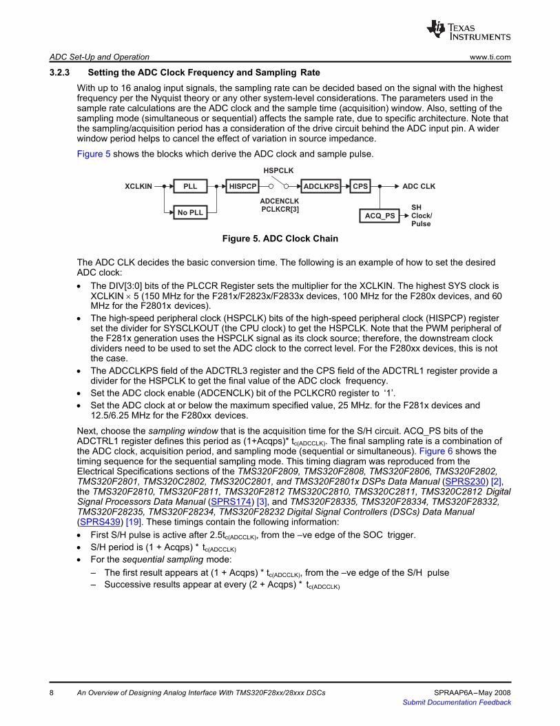
3.2.3 Setting the ADC Clock Frequency and Sampling Rate With up to 16 analog input signals, the sampling rate can be decided based on the signal with the highest frequency per the Nyquist theory or any other system-level considerations. The parameters used in the sample rate calculations are the ADC clock and the sample time (acquisition) window. Also, setting of the sampling mode (simultaneous or sequential) affects the sample rate, due to specific architecture. Note that the sampling/acquisition period has a consideration of the drive circuit behind the ADC input pin. A wider window period helps to cancel the effect of variation in source impedance. Figure 5 shows the blocks which derive the ADC clock and sample pulse.
HSPCLK
XCLKIN ADC CLK
ADCENCLK PCLKCR[3]
Figure 5. ADC Clock Chain
SH Clock/ Pulse
The ADC CLK decides the basic conversion time. The following is an example of how to set the desired ADC clock: • The DIV[3:0] bits of the PLCCR Register sets the multiplier for the XCLKIN. The highest SYS clock is
XCLKIN × 5 (150 MHz for the F281x/F2823x/F2833x devices, 100 MHz for the F280x devices, and 60 MHz for the F2801x devices).
• The high-speed peripheral clock (HSPCLK) bits of the high-speed peripheral clock (HISPCP) register set the divider for SYSCLKOUT (the CPU clock) to get the HSPCLK. Note that the PWM peripheral of the F281x generation uses the HSPCLK signal as its clock source; therefore, the downstream clock dividers need to be used to set the ADC clock to the correct level. For the F280xx devices, this is not the case.
• The ADCCLKPS field of the ADCTRL3 register and the CPS field of the ADCTRL1 register provide a divider for the HSPCLK to get the final value of the ADC clock frequency.
• Set the ADC clock enable (ADCENCLK) bit of the PCLKCR0 register to ‘1’. • Set the ADC clock at or below the maximum specified value, 25 MHz. for the F281x devices and
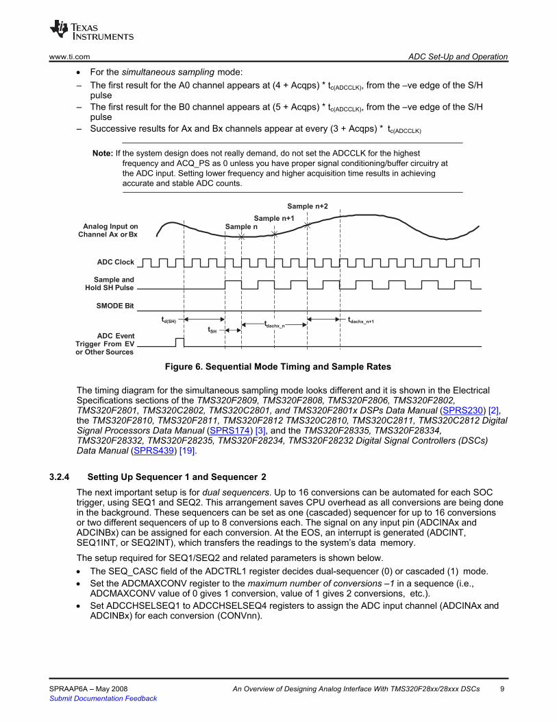
12.5/6.25 MHz for the F280xx devices. Next, choose the sampling window that is the acquisition time for the S/H circuit. ACQ_PS bits of the ADCTRL1 register defines this period as (1+Acqps)* tc(ADCCLK). The final sampling rate is a combination of the ADC clock, acquisition period, and sampling mode (sequential or simultaneous). Figure 6 shows the timing sequence for the sequential sampling mode. This timing diagram was reproduced from the Electrical Specifications sections of the TMS320F2809, TMS320F2808, TMS320F2806, TMS320F2802, TMS320F2801, TMS320C2802, TMS320C2801, and TMS320F2801x DSPs Data Manual (SPRS230) [2], the TMS320F2810, TMS320F2811, TMS320F2812 TMS320C2810, TMS320C2811, TMS320C2812 Digital Signal Processors Data Manual (SPRS174) [3], and TMS320F28335, TMS320F28334, TMS320F28332, TMS320F28235, TMS320F28234, TMS320F28232 Digital Signal Controllers (DSCs) Data Manual (SPRS439) [19]. These timings contain the following information: • First S/H pulse is active after 2.5tc(ADCCLK), from the –ve edge of the SOC trigger. • S/H period is (1 + Acqps) * tc(ADCCLK) • For the sequential sampling mode:
– The first result appears at (1 + Acqps) * tc(ADCCLK), from the –ve edge of the S/H pulse – Successive results appear at every (2 + Acqps) * tc(ADCCLK)
SPRAAP6A – May 2008 Submit Documentation Feedback
An Overview of Designing Analog Interface With TMS320F28xx/28xxx DSCs 9
ADC Set-Up and Operation www.ti.com
• For the simultaneous sampling mode: – The first result for the A0 channel appears at (4 + Acqps) * tc(ADCCLK), from the –ve edge of the S/H
pulse – The first result for the B0 channel appears at (5 + Acqps) * tc(ADCCLK), from the –ve edge of the S/H
pulse – Successive results for Ax and Bx channels appear at every (3 + Acqps) * tc(ADCCLK)
Note: If the system design does not really demand, do not set the ADCCLK for the highest frequency and ACQ_PS as 0 unless you have proper signal conditioning/buffer circuitry at the ADC input. Setting lower frequency and higher acquisition time results in achieving accurate and stable ADC counts.
Analog Input on Channel Ax or Bx
ADC Clock
Sample and Hold SH Pulse
Sample n+2 Sample n+1
Sample n
SMODE Bit
ADC Event Trigger From EV or Other Sources
td(SH) t
tSH
dachx_n
tdachx_n+1
Figure 6. Sequential Mode Timing and Sample Rates
The timing diagram for the simultaneous sampling mode looks different and it is shown in the Electrical Specifications sections of the TMS320F2809, TMS320F2808, TMS320F2806, TMS320F2802, TMS320F2801, TMS320C2802, TMS320C2801, and TMS320F2801x DSPs Data Manual (SPRS230) [2], the TMS320F2810, TMS320F2811, TMS320F2812 TMS320C2810, TMS320C2811, TMS320C2812 Digital Signal Processors Data Manual (SPRS174) [3], and the TMS320F28335, TMS320F28334, TMS320F28332, TMS320F28235, TMS320F28234, TMS320F28232 Digital Signal Controllers (DSCs) Data Manual (SPRS439) [19].
3.2.4 Setting Up Sequencer 1 and Sequencer 2
The next important setup is for dual sequencers. Up to 16 conversions can be automated for each SOC trigger, using SEQ1 and SEQ2. This arrangement saves CPU overhead as all conversions are being done in the background. These sequencers can be set as one (cascaded) sequencer for up to 16 conversions or two different sequencers of up to 8 conversions each. The signal on any input pin (ADCINAx and ADCINBx) can be assigned for each conversion. At the EOS, an interrupt is generated (ADCINT, SEQ1INT, or SEQ2INT), which transfers the readings to the system’s data memory. The setup required for SEQ1/SEQ2 and related parameters is shown below. • The SEQ_CASC field of the ADCTRL1 register decides dual-sequencer (0) or cascaded (1) mode. • Set the ADCMAXCONV register to the maximum number of conversions –1 in a sequence (i.e.,
ADCMAXCONV value of 0 gives 1 conversion, value of 1 gives 2 conversions, etc.). • Set ADCCHSELSEQ1 to ADCCHSELSEQ4 registers to assign the ADC input channel (ADCINAx and
ADCINBx) for each conversion (CONVnn).

10 An Overview of Designing Analog Interface With TMS320F28xx/28xxx DSCs SPRAAP6A – May 2008 Submit Documentation Feedback
ADC Set-Up and Operation www.ti.com
• The sequencer is triggered when ADCTRL2’s SOC_SEQ1 or SOC_SEQ2 bit = 1, as a software trigger. Alternatively, this condition can be set by PWM or an external pulse on the general-purpose input/output (GPIO) pin to synchronize the start of sequence with a PWM or an external event. For PWM trigger, the ADC SOC enable (SOCAEN and/or SOCBEN) and SOC trigger qualifier option (SOCASEL and/or SOCBSEL) within the ETSEL register of the PWM peripheral must be set. Note that the first channel in the sequencer is sampled after 2.5 ADC clock cycles.
• By setting the CONT_RUN bit of ADCTRL1 to 1, the ADC continues to convert channels, based on the SEQ_OVRD bit. This provides contiguous conversion of analog input. By setting this bit to 0, the sequencer operates in start-stop mode. The sequencer stops at EOS, and starts only when the new SOC trigger arrives.
• Review the ADCTRL2 register data for additional setup parameters related to the sequencers. Note that SOC_SEQ1, SOC_SEQ2, and related bits select the trigger signal to start a sequencer. Each trigger signal converts all the channels set for a sequencer. However, these signals are not used to start the conversion of every or a particular channel in a sequence.
3.2.5 Simultaneous and Sequential Sampling Mode
For the signals that need to be sampled at the same instance (e.g., voltage and current), simultaneous sampling mode is selected. Then, the signals at Ax and Bx inputs are sampled simultaneously using S/H-A and S/H-B sample-and-hold circuits. The pairs of channels selected are A0/B0, A1/B1, etc., not explicitly A2/B4 or A6/B2, etc. Resulting counts are held in ADCRESULT0/ADCRESULT1 (and so on) register pairs. As mentioned in Section 3.3.2, the sampling rate calculation depends on whether simultaneous or sequential sampling mode is selected. For more detailed information, see the ADC Electrical Specifications section of the device-specific data sheets. Set the SMODE_SEL bit of the ADCTRL3 register to 0 for sequential mode and to 1 for simultaneous mode.
3.3 ADC Interrupts and Interrupt Setting Using the PIE Block
The resulting counts of each conversion are stored in the ADCRESULTn registers, based on the setting of the sequencer(s). Note that the counts are held in the bit field [15:4] of these registers. Simultaneously, the counts are also stored in the set of the Mirror ADC registers (0xB00) with the data already right-justified, (i.e., bit field [11:0]). The system’s main routine can read these values any time and they are updated during every sequence. Once the sequencer completes the conversion of the last channel in the sequence, it generates an interrupt. The EOS interrupt can be used to synchronize the transfer of the ADC counts from the ADCRESULTn registers to the system memory. These interrupts are ADCINT, SEQ1INT and SEQ2INT (ADCINT alone, for F281x devices).They are multiplexed through the peripheral interrupt expander (PIE) block with the interrupt signals from other peripherals to connect them to the CPU (see Figure 7).

SPRAAP6A – May 2008 Submit Documentation Feedback
An Overview of Designing Analog Interface With TMS320F28xx/28xxx DSCs 11
ADC Set-Up and Operation www.ti.com
INT1 INT2
1
MUX
INT11 INT12
(Flag)
INTx MUX
(Flag) PIEACKx (Enable)
Global Enable
0
(Enable)
IFR(12:1) IER(12:1) INTM
INTx.1
From Peripherals or External Interrupts
INTx.2
INTx.3
INTx.4
INTx.5
INTx.6
INTx.7
INTx.8
(Enable Flag) PIEIERx(8:1) PIEIFRx(3:1)
Figure 7. ADC Interrupts Multiplexed via PIE Block
The PIE block multiplexes numerous interrupt sources into a smaller set of interrupt inputs. The path for ADC interrupts is set using the PIE registers. For completion purpose, this procedure is explained in the following paragraphs. Designers familiar with PIE architecture can skip this section. See the PIE architecture in Figure 7 and also the PIE table from the device-specific data sheets. Each peripheral of the F28xxx devices is able to generate multiple interrupt signals for the efficient operation. These interrupts are generated within a peripheral block, multiplexed to 12 INTx lines with selection/read control within the PIE block and processed in the CPU block. The interrupts are grouped into blocks of eight and each group is fed into one of 12 CPU interrupt lines (INT1 to INT12). Each of 96 interrupts is supported by its own vector stored in a dedicated RAM block that can be overwritten. In short, a total of 96 interrupt sources (all are not used) are reduced to 12 INTx signals, which translates to 12 AND gates (each opened by a PIEACKx signal; x = 1 to 12). The CPU block has separate Flags and enable schemes for these 12 INTx signals. Figure 7 shows the flow of these peripheral interrupt control signals and their logic level.
CPU
12 An Overview of Designing Analog Interface With TMS320F28xx/28xxx DSCs SPRAAP6A – May 2008 Submit Documentation Feedback
DMA and Calibration Functionality in F2823x and F2833x Families www.ti.com
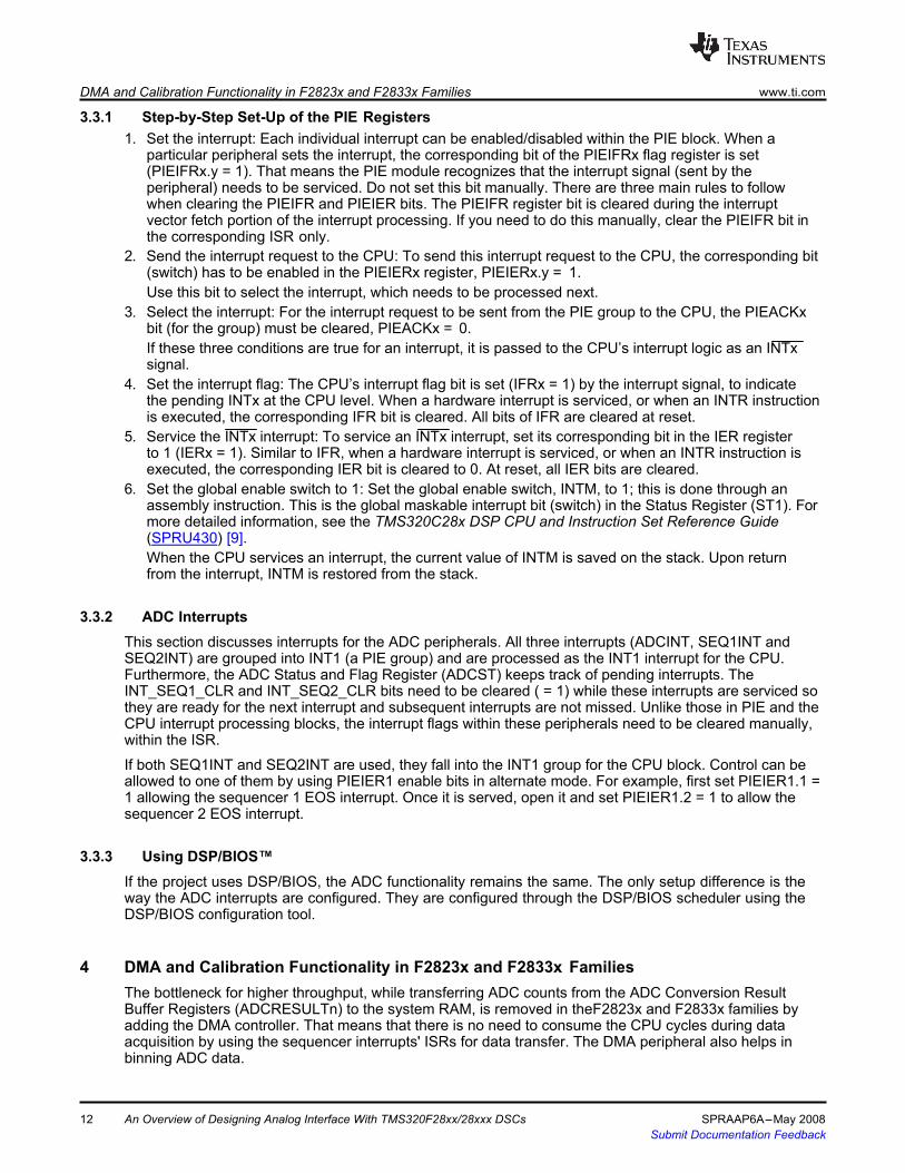
3.3.1 Step-by-Step Set-Up of the PIE Registers 1. Set the interrupt: Each individual interrupt can be enabled/disabled within the PIE block. When a
particular peripheral sets the interrupt, the corresponding bit of the PIEIFRx flag register is set (PIEIFRx.y = 1). That means the PIE module recognizes that the interrupt signal (sent by the peripheral) needs to be serviced. Do not set this bit manually. There are three main rules to follow when clearing the PIEIFR and PIEIER bits. The PIEIFR register bit is cleared during the interrupt vector fetch portion of the interrupt processing. If you need to do this manually, clear the PIEIFR bit in the corresponding ISR only.
2. Send the interrupt request to the CPU: To send this interrupt request to the CPU, the corresponding bit (switch) has to be enabled in the PIEIERx register, PIEIERx.y = 1. Use this bit to select the interrupt, which needs to be processed next.
3. Select the interrupt: For the interrupt request to be sent from the PIE group to the CPU, the PIEACKx bit (for the group) must be cleared, PIEACKx = 0. If these three conditions are true for an interrupt, it is passed to the CPU’s interrupt logic as an INTx signal.
4. Set the interrupt flag: The CPU’s interrupt flag bit is set (IFRx = 1) by the interrupt signal, to indicate the pending INTx at the CPU level. When a hardware interrupt is serviced, or when an INTR instruction is executed, the corresponding IFR bit is cleared. All bits of IFR are cleared at reset.
5. Service the INTx interrupt: To service an INTx interrupt, set its corresponding bit in the IER register to 1 (IERx = 1). Similar to IFR, when a hardware interrupt is serviced, or when an INTR instruction is executed, the corresponding IER bit is cleared to 0. At reset, all IER bits are cleared.
6. Set the global enable switch to 1: Set the global enable switch, INTM, to 1; this is done through an assembly instruction. This is the global maskable interrupt bit (switch) in the Status Register (ST1). For more detailed information, see the TMS320C28x DSP CPU and Instruction Set Reference Guide (SPRU430) [9]. When the CPU services an interrupt, the current value of INTM is saved on the stack. Upon return from the interrupt, INTM is restored from the stack.
3.3.2 ADC Interrupts
This section discusses interrupts for the ADC peripherals. All three interrupts (ADCINT, SEQ1INT and SEQ2INT) are grouped into INT1 (a PIE group) and are processed as the INT1 interrupt for the CPU. Furthermore, the ADC Status and Flag Register (ADCST) keeps track of pending interrupts. The INT_SEQ1_CLR and INT_SEQ2_CLR bits need to be cleared ( = 1) while these interrupts are serviced so they are ready for the next interrupt and subsequent interrupts are not missed. Unlike those in PIE and the CPU interrupt processing blocks, the interrupt flags within these peripherals need to be cleared manually, within the ISR. If both SEQ1INT and SEQ2INT are used, they fall into the INT1 group for the CPU block. Control can be allowed to one of them by using PIEIER1 enable bits in alternate mode. For example, first set PIEIER1.1 = 1 allowing the sequencer 1 EOS interrupt. Once it is served, open it and set PIEIER1.2 = 1 to allow the sequencer 2 EOS interrupt.
3.3.3 Using DSP/BIOS™
If the project uses DSP/BIOS, the ADC functionality remains the same. The only setup difference is the way the ADC interrupts are configured. They are configured through the DSP/BIOS scheduler using the DSP/BIOS configuration tool.
4 DMA and Calibration Functionality in F2823x and F2833x Families
The bottleneck for higher throughput, while transferring ADC counts from the ADC Conversion Result Buffer Registers (ADCRESULTn) to the system RAM, is removed in theF2823x and F2833x families by adding the DMA controller. That means that there is no need to consume the CPU cycles during data acquisition by using the sequencer interrupts' ISRs for data transfer. The DMA peripheral also helps in binning ADC data.
SPRAAP6A – May 2008 Submit Documentation Feedback
An Overview of Designing Analog Interface With TMS320F28xx/28xxx DSCs 13
DMA and Calibration Functionality in F2823x and F2833x Families www.ti.com
The F2823x and F2833x devices also include the ADC Offset Trim Register (ADCOFFTRIM) (as in F280x described in Section 6) and the ADC_cal() routine, programmed into TI reserved OTP memory. The boot ROM automatically calls the ADC_cal() routine which can also be called from an application.
4.1 Overview of DMA Peripheral The DMA module is an event-based machine. It requires a peripheral interrupt trigger to start a DMA transfer. There are six DMA channels and each can be configured independently for different trigger sources. Each channel also generates its own PIE interrupt to inform the CPU when the DMA transfer has either started or completed. Out of these six channels, Channel 1 can be configured as a higher priority than the rest of the five channels. This feature is important for ADC transfers. Using Channel 1 in high-priority mode ensures that the data/counts from every trigger are transferred. The DMA has unique state machine and tightly coupled address control logic. This address control logic allows for rearrangement of the block of data during the transfer, as well as the process of ping-ponging data between buffers. As far as ADC is concerned, SEQ1INT or SEQ2INT signals can be set as DMA trigger source for any channel. Apart from the ADC Memory Mapped Result Registers, the following memory resources are connected to the DMA bus: • XINTF Zones 0, 6 & 7 • L4 SARAM • L5 SARAM • L6 SARAM • L7 SARAM For the additional details regarding DMA pipeline timings, throughput rate, and the DMA state diagram, see the TMS320x2833x Direct Memory Access (DMA) Module Reference Guide (SPRUFB8) [17].
4.2 DMA Transfer Control A simplified hardware state machine flow is shown in Figure 8. The inner loop transfers a burst of data on receiving the trigger (SEQ1 or 2 interrupt). That is the smallest amount of data transferred at one time; its size is defined by the BURST_SIZE register. For the ADC, it corresponds to the number of conversions completed in one sequence. The outer loop defines how many bursts are performed in the entire transfer (bursts/transfer). Its size is set by a 16-bit TRANSFER_SIZE register. One CPU interrupt (DMA interrupt) is generated for each transfer and it can be configured to occur at the beginning or at the end of the transfer via MODE.CHx[CHINTMODE] bit. This bit can be used to keep any single channel from monopolizing the DMA bus. The bursts’ source address and destination address are set by using SRC_ADDR and DST_ADDR registers. During the burst loop, after each word is transferred, a signed value from the appropriate BURST_STEP register is added to the active SRC/DST_ADDR register. This feature is useful to store the counts from each ADC channel in the respective bins, within a transfer.

14 An Overview of Designing Analog Interface With TMS320F28xx/28xxx DSCs SPRAAP6A – May 2008 Submit Documentation Feedback
DMA and Calibration Functionality in F2823x and F2833x Families www.ti.com
Moved “Burst_Size”
Words ?
Yes
Moved “Transfer_Size”
Bursts ?
No
Yes
Add Transfer Step to Address
Pointer
Wait for Event to Start/Continue
Transfer
Read/Write Data
Point Where Other Pending Channels
are Serviced
Point Where CH1 can Interrupt
Other Channels
Figure 8. Simplified Hardware State Machine Flow
For example, if you set ADC for five conversions (from five channels) using Sequencer 1 and use DMA triggered by SEQ1INT, then store three consecutive sequences in a data buffer: • BURST_SIZE = 4 (5 words/burst) • TRANSFER_SIZE = 2 (3 bursts/transfer) By creating the address offset, using BURST_STEP and TRANSFER_STEP for source registers and destination registers, the data can be arranged in consecutive bins as shown in Figure 9.
Burst_Size*
* Size registers are N–1
Source Registers
ADDR.shadow BURST_STEP
5 Words/Burst 3 Bursts/Transfer
ADC Result Registers
L7 RAM
0xF000 0xF001 0xF002 0xF003 0xF004
Destination Registers
ADDR.shadow BURST_STEP
Figure 9. Address Control
End Transfer
0x0002 0x0004
No Add Burst Step to Address
Pointer
CH0 CH0 CH0 CH1 CH1 CH1 CH2 CH2 CH2 CH3 CH3 CH3 CH4 CH4 CH4
0x00000B00 0x0001 0xFFFC
0x0000F000 0x0003 0xFFF5
0x0B00 CH0 CH0 CH0 0xF005 0x0B01 CH1 CH1 CH1 0xF006 0x0B02 CH2 CH2 CH2 0xF007
(–4) 0x0B03 CH3 CH3 CH3 0xF008 0x0B04 CH4 CH4 CH4 0xF009
Time
0xF00A 0xF00B
0xF00C 0xF00D (–11) 0xF00E

SPRAAP6A – May 2008 Submit Documentation Feedback
An Overview of Designing Analog Interface With TMS320F28xx/28xxx DSCs 15
DMA and Calibration Functionality in F2823x and F2833x Families www.ti.com
There is another method to modify the active address pointer after each burst called wrapping, which loads the wrap address into the active address pointer. Address wrapping occurs when a number of bursts specified by the appropriate Source/Destination Wrap Size Register (SRC/DST_WRAP_SIZE) completes. Each DMA channel contains two shadowed wrap address pointers, SRC_BEG_ADDR and DST_BEG_ADDR, allowing the source and destination wrapping to be independent of each other. Like the SRC_ADDR and DST_ADDR registers, the active SRC/DST_BEG_ADDR registers are loaded from their shadow counterpart at the beginning of a transfer. When the specified number of bursts has occurred, a two part wrap procedure takes place: • The appropriate active SRC/DST_BEG_ADDR register is incremented by the signed value contained in
the SRC/DST_WRAP_STEP register, then • The new active SRC/DST_BEG_ADDR register is loaded into the active SRC/DST_ADDR register. Additionally, the wrap counter (SRC/DST_WRAP_COUNT) register is reloaded with the SRC/DST_WRAP_SIZE value to setup the next wrap period. This allows the channel to wrap multiple times within a single transfer. Combined with the first bullet above, this allows the channel to address multiple buffers within a single transfer. The DMA contains both an active and shadow set of the following address pointers. When a DMA transfer begins, the shadow register set is copied to the active working set of registers. This allows you to program the values of the shadow registers for the next transfer while the DMA works with the active set. It also allows you to implement ping-pong buffer schemes without disrupting the DMA channel execution. Wrap function allows to store the data into two buffers with large address reach (say one in internal on-chip RAM and another in external RAM)
4.2.1 ADC Sync Feature This DMA provides a hardware method of synchronizing to the ADC Sequencer 1 interrupt (SEQ1INT) when the ADC is running in continuous conversion mode (CONT_RUN = 1) with the sequencer override function enabled. In this mode, the ADC is continuously converting the ADC channels without resetting the sequencer pointer at the end of each sequence. Since the DMA does not know which ADC RESULT register the sequencer pointer is pointing to when it receives a trigger, there is a potential for the DMA and the ADC to be out of sync. For this reason, when the ADC is configured in this mode, it provides a synchronization signal to the DMA each time an event trigger is generated for a sequence starting at the RESULT0 register. The DMA expects this signal to line up with a wrap procedure or the beginning of a transfer. If it does not, a re-sync procedure occurs using the wrap function.
4.3 ADC Overrun
When a peripheral trigger is received by the DMA, the PERINTFLG bit in CONTROL register is set. It is cleared when the burst for that channel starts. If however, before the burst is started and the PERINTFLG is still set, another trigger arrives from the same peripheral, it will be lost. This condition will set the OVERFLG bit in the CONTROL register. By setting the overrun interrupt, the channel generates a PIE interrupt. For the working code of the ADC’s data transfer using DMA, see the adc_dma example from Download: C2833x/C2823x C/C++ Header Files and Peripheral Examples (SPRC530) [16].
4.4 ADC Calibration The F2823x and F2833x devices include the ADC_cal() routine, which is programmed into TI reserved OTP memory, and in addition to the ADC Offset Register that is similar to the F280x devices. The boot ROM automatically calls the ADC_cal() routine to initialize the ADCREFSEL and ADCOFFTRIM registers with the specific calibration data. During the regular operation, the calibration process occurs automatically; no action is required by you. Note that this ADC_cal routine brings the ADC up to the specifications in the data sheets. For further improvements in the offset and gain errors, the calibration procedure mentioned in Section 6 needs to be added. Two different methods for calling ADC_cal() within your application are explained in the TMS320x2833x Analog-to-Digital Converter (ADC) Module Reference Guide (SPRU812) [18].
16 An Overview of Designing Analog Interface With TMS320F28xx/28xxx DSCs SPRAAP6A – May 2008 Submit Documentation Feedback
Schematic and Board Design www.ti.com
5 Schematic and Board Design Attention should be paid to the schematic design and board layout to achieve required results, consistency of operation, and to minimize total conversion error. It is an important aspect of the design that the on-chip ADC module of the F28xx devices operates in the vicinity of many high-speed digital signals. These design tips are case-to-case dependent and some of them may not be needed in your application. However, under extreme noisy conditions, it is probably a good practice to follow all of these guidelines.
5.1 Board Design Tips to Get the Best Performance From the F28xx/F28xxx ADCs • Terminate any unused ADCIN pins to the analog ground. These are defined as input pins and an open
pin of this CMOS device picks up the voltages (noise) around it. Ensure that any of the digital signal pins are not terminated to the analog ground.
• The voltage applied to the ADCIN pins should be restricted between 0 V–3 V. If it exceeds this limit on any channel, it temporarily affects the conversions on the other channels. If the signal conditioning circuit used for the input analog signal needs to use any higher supply voltage (i.e., 5 V), it is recommended that a buffer stage that scales this signal to < 3 V be used before connecting to the ADCIN pin.
• If you need to monitor DC voltages higher than 3.0 V, the resistor divider should be followed by an op-amp buffer stage. By connecting the resistor divider directly to the ADCIN pin violates low source impedance requirement and conversion counts will see large errors.
• Place a 0.1-µF decoupling capacitor for every power (VDD) pin of the DSP and all other active devices. Use higher quality ceramic dielectrics which have better high-frequency performance.
• Either set all unused GPIO pins as outputs and leave them unconnected or set them as inputs and use fairly heavy external pull down resistors, (i.e., 3–10 kΩ).
• Tie the ADCLO pin to VSSA at the pin or with short and wide trace.
5.2 Power Supply Recommendations • Isolate the analog 3.3-V supply rail from other digital 3.3-V rails. It is better to use a completely
separate voltage regulator for analog 3.3 V supply, particularly if the load on analog 3.3 V rail is fairly large.
• The LDO type of voltage regulators are preferred over switchers. The voltage tolerance should be within 5% and ripple typically well below 20 mV when the CPU is running at the maximum speed.
• A separate analog ground should be used to terminate all analog signals and preferably in a star connection. The common point for analog and digital grounds should be at the ground pin of the filter capacitor on an analog 3.3-V rail or regulator. Ensure that the return current from any digital signal does not flow into this analog ground plane.
• The recommended power-supply sequencing is that the core should be powered up first, followed by the I/O, and then the analog voltage supplies. The input voltages to the ADCINxx pins should be applied only after the analog voltage supply is applied.
• If using an external voltage reference, use a stable VREF supply with no variation during run time either due to board noise or supply noise. Individual Op-amp buffer stages should be used on each VREF rail. Provide 1 nF and 10 µF low ESR capacitors on each reference line. Do not connect these signals to any other circuit in order to avoid interference. A typical schematic is shown in the TMS320x281x DSP Analog-to-Digital Converter (ADC) Reference Guide (SPRU060) [5].

SPRAAP6A – May 2008 Submit Documentation Feedback
An Overview of Designing Analog Interface With TMS320F28xx/28xxx DSCs 17
www.ti.com Schematic and Board Design
5.3 Board Layout The expected performance can be achieved only with a good board layout. There are many books, application reports, and documents describing the best practices. A few of the recommendations are shown below. • Place all the external components close to the ADC-related pins. Particular care should be taken to
place the components for external reference voltage close to the ADCREFP and ADCREFM pins. • The board layout should have no digital lines crossing, particularly if this DSP interfaces to a motor and
power electronics board. Avoid routing analog signals in the area that have switching digital activity, like clock oscillator, data/address buses, etc.
• Use ground plane and power plane. • Use single point and wide trace to connect analog and digital ground planes. • Pay attention to the trace width and length for low level analog signals. Use wider tracks to minimize
inductance and reduce noise pickup. • It is recommended that a separate ground plane be used. That keeps the ADC return paths at low
impedances. If the ground plane is not possible, using wide and short traces for ground return are recommended. Poor ground can affect system performance in unpredictable ways, sometimes not even indicating that poor ground problems exist.
Figure 10. Layout Example 1: Component Placement
Figure 11. Layout Example 2: Routing/Traces

18 An Overview of Designing Analog Interface With TMS320F28xx/28xxx DSCs SPRAAP6A – May 2008 Submit Documentation Feedback
ADC Calibration www.ti.com
6 ADC Calibration Like all ADCs, the inherent gain and offset errors are associated with the F28xx/F28xxx ADC. The maximum values for both types of error for F280x/F280xx devices are ± 60 LSB. The F281x ADC has a maximum offset error of ± 80 LSB and a maximum gain error of ± 200 LSB. The F2823x/F2833x devices have lower error number: max offset error of ± 15 LSB and max gain error of ± 30 LSB.Figure 12 describes the impact of these errors on actual counts. Some applications may require correcting them to improve the accuracy, (i.e., to improve the effective number of bits (ENOB)).
Figure 12. ADC Conversion Transfer Function
The F280x, F2823x and F2833x ADC supports offset correction via the ADCOFFTRIM. It is a 9-bit signed value that trims both positive and negative offsets. This trim performs in the analog domain, which preserves the native range of the ADC; opposed to a post conversion digital trim that corrects the offset, but loses range on the ADC output. Thus, in the case of the F280xx devices, the offset error can be corrected without requiring external circuitry. A software-based calibration procedure is adapted to combat this situation. For more detailed information regarding calibration procedures, see F2810, F2811, F2812 ADC Calibration (SPRA989) [10] (for F281x) and TMS320280x and TMS320F2801x ADC Calibration (SPRAAD8) [11] (for F280xx). These documents also include associated code.
7 Additional Support
This section discusses a few software packages which are useful when starting a design and once the ADC is functional.
7.1 Filter Library Applying digital filters to the digitized data is a common requirement for digital signal processing. Download TMS320C28x Filter Library - SPRC082 (http://www-s.ti.com/sc/techlit/sprc082.zip) [12] provides filter library code for TMS320C28x™ DSPs. It includes both types of digital filter (16-bit) modules: finite impulse response (FIR) and infinite impulse response (IIR). The main feature of this code is the use of the DMAC instruction which does the calculations for two taps in a single CPU cycle. The reference guide embedded in the zip file explains this in complete details.
Actual Gain Ideal Gain
Digitized Signal
Offset
Ideal Signal
Analog Signal
Controlled by INL/DNL Specs
SPRAAP6A – May 2008 Submit Documentation Feedback
An Overview of Designing Analog Interface With TMS320F28xx/28xxx DSCs 19
www.ti.com References
7.2 Example Code Additional example projects are available from: Download C281x C/C++ Header Files and Peripheral Examples - SPRC097 (http://www-s.ti.com/sc/techlit/sprc097.zip) [13] (for F281x devices), Download: C280x, C2801x C/C++ Header Files and Peripheral Examples - SPRC191 (http://www-s.ti.com/sc/techlit/sprc191.zip) [14] (for F280xx devices), and Download: C2804x C/C++ Header Files and Peripheral Examples - SPRC324 (http://www-s.ti.com/sc/techlit/sprc324.zip) [15] (for F2804x devices).
8 References
1. Understanding Data Converters (SLAA013). 2. TMS320F2809, TMS320F2808, TMS320F2806, TMS320F2802, TMS320F2801, TMS320C2802,
TMS320C2801, and TMS320F2801x DSPs Data Manual (SPRS230) 3. TMS320F2810, TMS320F2811, TMS320F2812, TMS320C2810, TMS320C2811,TMS320C2812 Digital
Signal Processors Data Manual (SPRS174) 4. TMS320x280x, 2801x, 2804x DSP Analog-to-Digital Converter(ADC) Reference Guide (SPRU716) 5. TMS320x281x DSP Analog-to-Digital Converter (ADC) Reference Guide (SPRU060) 6. Buffer Op Amp to ADC Circuit Collection (SLOA098) 7. A Glossary of Analog-to-Digital Specifications and Performance Characteristics (SBAA147) 8. Understanding the TMS320F2808, F2806 and F2801 ADC for Embedded Control Applications
(SPRP297) 9. TMS320C28x DSP CPU and Instruction Set Reference Guide (SPRU430) 10. F2810, F2811, F2812 ADC Calibration (SPRA989) 11. TMS320280x and TMS320F2801x ADC Calibration (SPRAAD8) 12. Download TMS320C28x Filter Library - SPRC082 (http://www-s.ti.com/sc/techlit/sprc082.zip) 13. Download C281x C/C++ Header Files and Peripheral Examples - SPRC097
(http://www-s.ti.com/sc/techlit/sprc097.zip) 14. Download: C280x, C2801x C/C++ Header Files and Peripheral Examples - SPRC191
(http://www-s.ti.com/sc/techlit/sprc097.zip) 15. Download: C2804x C/C++ Header Files and Peripheral Examples - SPRC324
(http://www-s.ti.com/sc/techlit/sprc324.zip) 16. Download: C2833x/C2823x C/C++ Header Files and Peripheral Examples (SPRC530) 17. TMS320x2833x Direct Memory Access (DMA) Module Reference Guide (SPRUFB8) 18. TMS320x2833x Analog-to-Digital Converter (ADC) Module Reference Guide (SPRU812) 19. TMS320F28335, TMS320F28334, TMS320F28332, TMS320F28235, TMS320F28234,
TMS320F28232 Digital Signal Controllers (DSCs) Data Manual (SPRS439)
20 SPRAAP6A – May 2008 Submit Documentation Feedback
Appendix A www.ti.com
Appendix A F280xx and F281x Differences
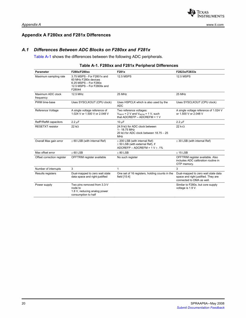
A.1 Differences Between ADC Blocks on F280xx and F281x Table A-1 shows the differences between the following ADC peripherals.
Table A-1. F280xx and F281x Peripheral Differences
Parameter F280x/F280xx F281x F2823x/F2833x Maximum sampling rate 3.75 MSPS - For F2801x and 12.5 MSPS 12.5 MSPS
60 MHz F280x devices 6.25 MSPS – For F280x 12.5 MSPS – For F2809x and
F28044
Maximum ADC clock 12.5 MHz 25 MHz 25 MHz frequency
PWM time-base Uses SYSCLKOUT (CPU clock) Uses HSPCLK which is also used by the Uses SYSCLKOUT (CPU clock) ADC
Reference Voltage A single voltage reference of Two reference voltages: A single voltage reference of 1.024 V 1.024 V or 1.500 V or 2.048 V VREFP = 2 V and VREFM = 1 V, such or 1.500 V or 2.048 V that ADCREFP – ADCREFM = 1 V
RefP/RefM capacitors 2.2 µF 10 µF 2.2 µF RESETXT resistor 22 kΩ 24.9 kΩ for ADC clock between 22 k-Ω
1– 18.75 MHz
20 kΩ for ADC clock between 18.75 – 25
MHz
Overall Max gain error ± 60 LSB (with internal Ref) ± 200 LSB (with internal Ref) ± 30 LSB (with internal Ref) ± 50 LSB (with external Ref), if
ADCREFP – ADCREFM = 1 V ± .1%
Max offset error ± 60 LSB ± 80 LSB ± 15 LSB Offset correction register OFFTRIM register available No such register OFFTRIM register available. Also
includes ADC calibration routine in OTP memory.
Number of interrupts 3 1 3 Results registers Dual-mapped to zero wait state One set of 16 registers, holding counts in the Dual-mapped to zero wait state data
data space and right-justified field [15:4] space and right justified. They are connected to DMA as well. Power supply Two pins removed from 3.3-V Similar to F280x, but core supply
node to voltage is 1.9 V. 1.8 V, reducing analog power
consumption to half

IMPORTANT NOTICE AND DISCLAIMER
TI PROVIDES TECHNICAL AND RELIABILITY DATA (INCLUDING DATASHEETS), DESIGN RESOURCES (INCLUDING REFERENCEDESIGNS), APPLICATION OR OTHER DESIGN ADVICE, WEB TOOLS, SAFETY INFORMATION, AND OTHER RESOURCES “AS IS”AND WITH ALL FAULTS, AND DISCLAIMS ALL WARRANTIES, EXPRESS AND IMPLIED, INCLUDING WITHOUT LIMITATION ANYIMPLIED WARRANTIES OF MERCHANTABILITY, FITNESS FOR A PARTICULAR PURPOSE OR NON-INFRINGEMENT OF THIRDPARTY INTELLECTUAL PROPERTY RIGHTS.These resources are intended for skilled developers designing with TI products. You are solely responsible for (1) selecting the appropriateTI products for your application, (2) designing, validating and testing your application, and (3) ensuring your application meets applicablestandards, and any other safety, security, or other requirements. These resources are subject to change without notice. TI grants youpermission to use these resources only for development of an application that uses the TI products described in the resource. Otherreproduction and display of these resources is prohibited. No license is granted to any other TI intellectual property right or to any thirdparty intellectual property right. TI disclaims responsibility for, and you will fully indemnify TI and its representatives against, any claims,damages, costs, losses, and liabilities arising out of your use of these resources.TI’s products are provided subject to TI’s Terms of Sale (www.ti.com/legal/termsofsale.html) or other applicable terms available either onti.com or provided in conjunction with such TI products. TI’s provision of these resources does not expand or otherwise alter TI’s applicablewarranties or warranty disclaimers for TI products.
Mailing Address: Texas Instruments, Post Office Box 655303, Dallas, Texas 75265Copyright © 2019, Texas Instruments Incorporated