an11403 tea1836xt greenchip smps control ic · document information an11403 tea1836xt greenchip...
TRANSCRIPT
AN11403TEA1836XT GreenChip SMPS control ICRev. 1 — 18 April 2014 Application note
Document information
Info Content
Keywords TEA1836XT, DCM flyback converter, high efficiency, burst mode operation, low audible noise, high peak power, active X-capacitor discharge, low power consumption
Abstract The TEA1836XT is a high-featured low-cost DCM flyback converter controller. It provides a high efficiency at all power levels and very low no-load power consumption at nominal output voltage using burst mode operation.
Burst mode is enhanced to minimize the risk of audible noise.
The TEA1836XT is intended for power supplies up to 75 W that require extended high peak power capabilities in order to supply high power without requiring a PFC.
Typical applications are notebook adapters, printers, TVs or computer monitors.

NXP Semiconductors AN11403TEA1836XT GreenChip SMPS control IC
Revision history
Rev Date Description
v.1 20140418 first issue
AN11403 All information provided in this document is subject to legal disclaimers. © NXP Semiconductors N.V. 2014. All rights reserved.
Application note Rev. 1 — 18 April 2014 2 of 68
Contact informationFor more information, please visit: http://www.nxp.com
For sales office addresses, please send an email to: [email protected]

NXP Semiconductors AN11403TEA1836XT GreenChip SMPS control IC
1. Introduction
This application note describes the implementation of TEA1836XT functions in practical applications. Information is provided on converter design, including transformer considerations.
Each section/paragraph can be read as a standalone description with few cross-references to other parts of the application note or data sheet. Typical values are given to enhance the readability unless stated otherwise.
2. Features and applications
2.1 General features
• DCM flyback controller IC for low-cost applications
• Wide supply voltage range (up to 30 V; 35 V peak allowed for 100 ms)
• Integrated high-voltage start-up current source
• Continuous minimum VCC regulation during start-up and protection via the HV pin, allowing a small VCC capacitor to be used
• Reduced optocoupler current (100 A) in burst mode, enabling low power consumption in no-load while keeping the output voltage in regulation
• Converter switching frequencies and burst mode operation outside the audible area
• Integrated active X-capacitor discharge
• Adjustable soft start
• Power-down mode activated by the PROTECT pin
• 150 % peak power capability
2.2 Green features
• Low supply current during normal operation (0.6 mA without driver load)
• Low supply current during non-switching state in burst mode (0.2 mA)
• Valley switching for minimum switching losses
• Quasi resonant controller can be used in combination with NXP Semiconductors SR controllers for optimal efficiency performance
• Burst mode and frequency reduction mode with fixed minimum peak current to maintain high efficiency at low output power levels
2.3 Protection features
• Mains voltage independent OverPower Protection (OPP)
• Internal OverTemperature Protection (OTP)
• Integrated overpower time-out
• Integrated restart timer for system fault conditions
• Continuous mode protection using demagnetization detection
• Accurate OverVoltage Protection (OVP)
AN11403 All information provided in this document is subject to legal disclaimers. © NXP Semiconductors N.V. 2014. All rights reserved.
Application note Rev. 1 — 18 April 2014 3 of 68
NXP Semiconductors AN11403TEA1836XT GreenChip SMPS control IC
• General-purpose input for latched protection; can be used for external OverTemperature Protection (OTP)
• Driver maximum on-time protection
2.4 Applications
Typical applications are notebook adapters, printers, TVs or computer monitors.
3. Pinning
For the TEA1836xT three types of packages are available, TEA18361T, TEA18362T, and TEA18363T.
Pin numbers in this application note refer to the TEA18362T version.
3.1 Pin descriptions
Fig 1. TEA18361T pinning diagram
Fig 2. TEA18362T pinning diagram
Fig 3. TEA18363T pinning diagram
Table 1. TEA18362T pin descriptions
Pin number
Pin name Functional description summary
1 VCC IC supply voltage input and source for the internal HV start-up output. All internal circuits, except the high-voltage circuit, are supplied from this pin.
The buffer capacitor on the VCC pin can be charged in several ways:
• Internal High-Voltage (HV) start-up source
• Auxiliary winding from the flyback transformer
• External DC supply
IC operation is enabled when the voltage on the VCC pin reaches 14.9 V.
In burst mode operation, a new burst is initiated when the voltage on the VCC is 11 V. It prevents that the voltage drops to below the stop operation level.
The IC halts operation when the voltage on the VCC pin drops to below 9.9 V.
Shutdown reset is activated at 8.65 V.
2 GND ground connection; reference for other pins.
3 DRIVER MOSFET gate driver output
AN11403 All information provided in this document is subject to legal disclaimers. © NXP Semiconductors N.V. 2014. All rights reserved.
Application note Rev. 1 — 18 April 2014 4 of 68

NXP Semiconductors AN11403TEA1836XT GreenChip SMPS control IC
4 ISENSE current sense input
This pin senses the primary current through the MOSFET switch via an external resistor.
Soft start
Just before the converter starts, an internal current source charges the external soft start capacitor with 75 A. When the voltage on the ISENSE pin reaches 765 mV, the capacitor has been sufficiently charged. The current source is switched off and the controller starts switching with an on-time of 665 ns. The soft start capacitor now slowly discharges through the soft start resistor that is connected in parallel, slowly enabling the primary peak current to increase. When the ISENSE voltage is below 500 mV, the peak current regulation takes over with a minimum on-time of 325 ns. The capacitor value and the value of the parallel resistor can set the soft start time. These components must be placed close to the IC to prevent negative spikes from reaching the pin. The internal ESD protection diode can cause a DC offset by rectifying negative spikes. A resistor in series with the connection to the ISENSE pin can help to minimize this effect.
During soft start, the ISENSE pin constantly measures the voltage level on the pin. It limits the peak current by switching off the MOSFET when the voltage reaches Vopp(ISENSE) (= 500 mV). When the CTRL voltage drops below 5 V, the controller assumes that the output is in regulation and the start-up ends. The maximum sense voltage is increased allowing peak power.
Frequency reduction mode
In this mode, the peak current is kept constant by a fixed voltage of 207 mV on the ISENSE pin. The output voltage is regulated by controlling the switching frequency.
Leading-edge blanking
During the first 325 ns of each switching cycle, the ISENSE input is internally blanked to prevent the spike caused by parasitic capacitance triggering the peak current comparator prematurely.
Propagation delay
There is a delay between the moment the ISENSE comparator is triggered and the moment the MOSFET is switched off. During this time, the primary current continues to increase. How much it is able to increase depends on the di/dt slope and thus on the mains voltage. So the resulting peak current not only depends on the CTRL voltage but also on the mains voltage.
Overpower compensation for mains voltage by AUX sensing current
To enable the output power level to be independent of the mains voltage, an overpower compensation circuit regulates the output power based on the input voltage sensed on the AUX pin.
Overpower protection counter
When the voltage on the ISENSE pin exceeds the overpower protection level (between 295 mV and 500 mV depending on mains voltage), the overpower counter is started. When the overpower timer reaches 200 ms (40 ms during start-up) a restart is initiated.
In a TEA1836 latched version, the overpower detection circuit provides latched protection. The counter is reset after every cycle in which the protection level is not exceeded.
Overpower limiting
A maximum allowed ISENSE level (between 450 mV and 765 mV depending on mains voltage) limits the maximum peak power. When more power is drawn from the converter output, the output voltage drops (out of regulation).
Table 1. TEA18362T pin descriptions …continued
Pin number
Pin name Functional description summary
AN11403 All information provided in this document is subject to legal disclaimers. © NXP Semiconductors N.V. 2014. All rights reserved.
Application note Rev. 1 — 18 April 2014 5 of 68
NXP Semiconductors AN11403TEA1836XT GreenChip SMPS control IC
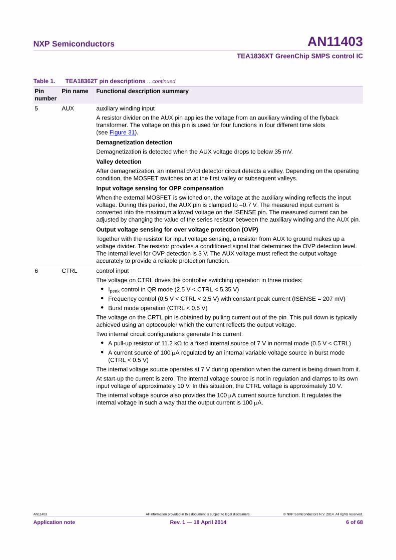
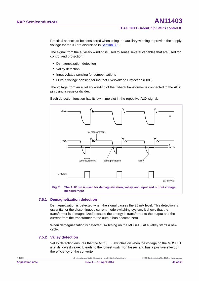
5 AUX auxiliary winding input
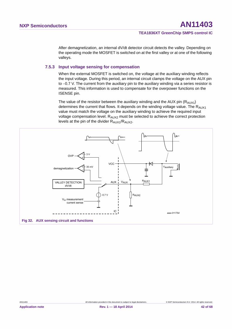
A resistor divider on the AUX pin applies the voltage from an auxiliary winding of the flyback transformer. The voltage on this pin is used for four functions in four different time slots (see Figure 31).
Demagnetization detection
Demagnetization is detected when the AUX voltage drops to below 35 mV.
Valley detection
After demagnetization, an internal dV/dt detector circuit detects a valley. Depending on the operating condition, the MOSFET switches on at the first valley or subsequent valleys.
Input voltage sensing for OPP compensation
When the external MOSFET is switched on, the voltage at the auxiliary winding reflects the input voltage. During this period, the AUX pin is clamped to 0.7 V. The measured input current is converted into the maximum allowed voltage on the ISENSE pin. The measured current can be adjusted by changing the value of the series resistor between the auxiliary winding and the AUX pin.
Output voltage sensing for over voltage protection (OVP)
Together with the resistor for input voltage sensing, a resistor from AUX to ground makes up a voltage divider. The resistor provides a conditioned signal that determines the OVP detection level. The internal level for OVP detection is 3 V. The AUX voltage must reflect the output voltage accurately to provide a reliable protection function.
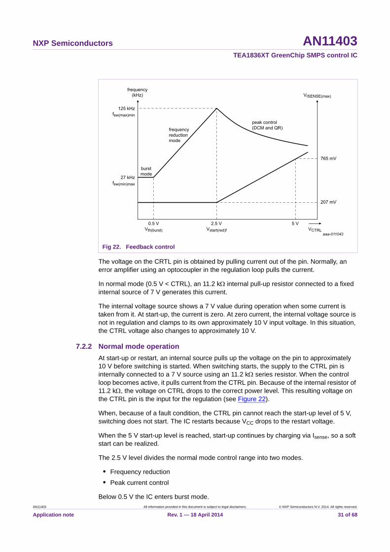
6 CTRL control input
The voltage on CTRL drives the controller switching operation in three modes:
• Ipeak control in QR mode (2.5 V < CTRL < 5.35 V)
• Frequency control (0.5 V < CTRL < 2.5 V) with constant peak current (ISENSE = 207 mV)
• Burst mode operation (CTRL < 0.5 V)
The voltage on the CRTL pin is obtained by pulling current out of the pin. This pull down is typically achieved using an optocoupler which the current reflects the output voltage.
Two internal circuit configurations generate this current:
• A pull-up resistor of 11.2 k to a fixed internal source of 7 V in normal mode (0.5 V < CTRL)
• A current source of 100 A regulated by an internal variable voltage source in burst mode (CTRL < 0.5 V)
The internal voltage source operates at 7 V during operation when the current is being drawn from it.
At start-up the current is zero. The internal voltage source is not in regulation and clamps to its own input voltage of approximately 10 V. In this situation, the CTRL voltage is approximately 10 V.
The internal voltage source also provides the 100 A current source function. It regulates the internal voltage in such a way that the output current is 100 A.
Table 1. TEA18362T pin descriptions …continued
Pin number
Pin name Functional description summary
AN11403 All information provided in this document is subject to legal disclaimers. © NXP Semiconductors N.V. 2014. All rights reserved.
Application note Rev. 1 — 18 April 2014 6 of 68

NXP Semiconductors AN11403TEA1836XT GreenChip SMPS control IC
Burst mode operation
An internal digital control system drives the burst mode switching using the feedback info on the CTRL pin. Minimum switching frequency is 25 kHz. Burst repetition is approximately 800 Hz. The minimum number of pulses in a single burst is 3. When the number of pulses exceeds 40, the system switches to normal mode.
To reduce current consumption to 235 A, internal circuits are switched off during the non-switching periods.
To monitor the output voltage continuously via the optocoupler current, the voltage on the CTRL pin is clamped to a minimum of 0.5 V during the burst. The current value is used for switching control. Switching stops when the current exceeds 750 A.
To ensure an equal starting condition for each burst cycle, the voltage on the CTRL pin is pulled low after each burst cycle (during 50 s).
When the device exits burst mode, the internal CTRL supply voltage is slowly regulated to 7 V to ensure consistent history-independent behavior in normal mode.
Normal mode operation
At start-up or restart, the CTRL pin is set to 7 V by an internal source before switching is started. When the control loop becomes active, it pulls current from the CTRL pin lowering the voltage to the correct power level.
7 PROTECT Protection and power-down mode control
The voltage on the PROTECT pin divides the system into three different modes:
• Normal mode (0.5 V < PROTECT < 1.45 V; IPROTECT = 75 A)
• Protection (0.2 V < PROTECT < 0.5 V; IPROTECT = 75 A when coming from normal mode or IPROTECT = 122 A when coming from power-down mode)
• Power-down mode (PROTECT < 0.2 V; IPROTECT = 47 A)
In the basic circuit configuration, an internal current source and an externally connected resistor to GND determine the voltage on the PROTECT pin. The externally connected resistor can be an NTC to provide external overtemperature protection.
Normal mode (0.5 V < PROTECT < 1.45 V)
The PROTECT voltage is limited to 1.45 V by the internal clamp function. At start-up, the current sources are active before the operation starts to set the normal mode starting condition.
Protection (0.2 V < PROTECT < 0.5 V)
Depending on IC tolerance, a latched protection is triggered after a 2 ms to 4 ms delay. The internal delay avoids unwanted triggering. To avoid triggering the protection mode, the protection pin must be pulled low faster than 2 ms when entering power-down mode.
Power-down mode (PROTECT < 0.2 V)
To activate power-down mode, the voltage can be pulled to GND level using an external switch. To increase the voltage to normal mode quickly, the current sourcing level is high (122 A) when releasing the PROTECT pin from power-down mode.
In power-down mode, the auxiliary winding supplies the IC.
Table 1. TEA18362T pin descriptions …continued
Pin number
Pin name Functional description summary
AN11403 All information provided in this document is subject to legal disclaimers. © NXP Semiconductors N.V. 2014. All rights reserved.
Application note Rev. 1 — 18 April 2014 7 of 68
NXP Semiconductors AN11403TEA1836XT GreenChip SMPS control IC
8 HV High-voltage start-up; active X-capacitor discharge
The HV pin incorporates three functions:
• High-voltage current source
• Mains voltage sensing input
• X-capacitor discharge
High-voltage current source
At start-up, the 1.1 mA HV current source is used to charge VCC, so that IC operation can start. Until VCC reaches the start-up level (14.9 V), the IC current consumption is limited to 40 A.
During shutdown mode, the HV source regulates the voltage on the VCC pin to 11.3 V using the on/off control.
Mains voltage sensing
During operation, the mains voltage is sensed by sampling the HV input current value every 1 ms. The HV input current is measured by pulling the HV input to 2.6 V for 20 s. This current value reflects the mains voltage value. The value of the external series resistors between mains (L/N) and the HV pin can set the start and stop levels.
When the current is above 663 A, start-up is enabled (brownin). When the current drops below 587 A for more than 30 ms, the operation is stopped (brownout). The 30 ms period is required to avoid that the system stops switching due to the zero crossings of the mains or during a short mains interruption.
During operation, conditional sensing control reduces the sampling frequency. When a mains voltage is detected, mains voltage sensing is halted for 6 ms (97 ms during burst mode) to improve efficiency.
Active X-capacitor discharge
When the mains voltage sensing does not detect a positive dV/dt (increasing values) for 28 ms, it assumes that the mains voltage is disconnected. It starts the X-capacitor discharge function. During the X-capacitor discharge, the HV pin is pulled low. The external X-capacitor is discharged through the external resistors.
Table 1. TEA18362T pin descriptions …continued
Pin number
Pin name Functional description summary
AN11403 All information provided in this document is subject to legal disclaimers. © NXP Semiconductors N.V. 2014. All rights reserved.
Application note Rev. 1 — 18 April 2014 8 of 68
NXP Semiconductors AN11403TEA1836XT GreenChip SMPS control IC
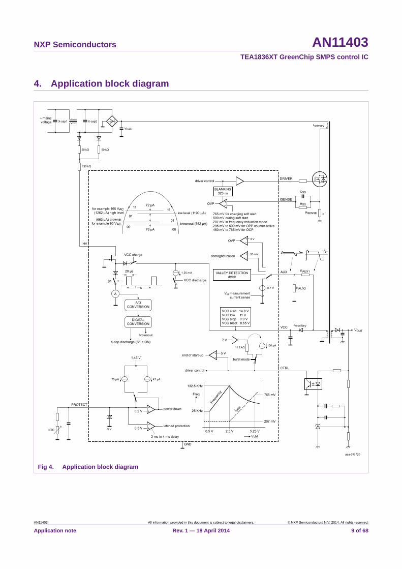
4. Application block diagram
Fig 4. Application block diagram
AN11403 All information provided in this document is subject to legal disclaimers. © NXP Semiconductors N.V. 2014. All rights reserved.
Application note Rev. 1 — 18 April 2014 9 of 68

NXP Semiconductors AN11403TEA1836XT GreenChip SMPS control IC
5. Flyback converter operating modes
This chapter describes the flyback converter operation modes that are implemented in the TEA1836XT. Section 6 contains an application guideline.
5.1 TEA1836XT flyback operating modes
The TEA1836XT features four different flyback operation modes:
• Quasi-Resonant (QR) mode (high power level)
• Discontinuous Conduction Mode (DCM) with fixed frequency (medium-high power level)
• Discontinuous Conduction Mode (DCM) with frequency reduction (medium-low power level)
• Burst mode (low power level)
Depending the output power, the system switches between operating modes. The goal is to provide the best performance for each power level. The best performance is based on the highest efficiency and the lowest losses.
A DCM flyback system is compatible with SR controllers for optimal efficiency performance.
Fig 5. TEA1836XT flyback operation modes
AN11403 All information provided in this document is subject to legal disclaimers. © NXP Semiconductors N.V. 2014. All rights reserved.
Application note Rev. 1 — 18 April 2014 10 of 68

NXP Semiconductors AN11403TEA1836XT GreenChip SMPS control IC
5.2 DCM flyback conversion
Figure 6 shows a basic circuit diagram and several waveforms of the flyback topology.
During tprim, the MOSFET is switched on. The current flows through the primary winding of the transformer and the MOSFET. The transformer is magnetized.
When the MOSFET is switched off, the drain voltage increases to a voltage that is the sum of the input voltage and the reflected output voltage (output voltage multiplied by the transformer turn ratio).
The voltage at the secondary turn increases and the output diode conducts current to the output. The transformer is demagnetized during tsec.
a. Basic circuit diagram
b. Waveforms
Fig 6. Flyback topology
AN11403 All information provided in this document is subject to legal disclaimers. © NXP Semiconductors N.V. 2014. All rights reserved.
Application note Rev. 1 — 18 April 2014 11 of 68
NXP Semiconductors AN11403TEA1836XT GreenChip SMPS control IC
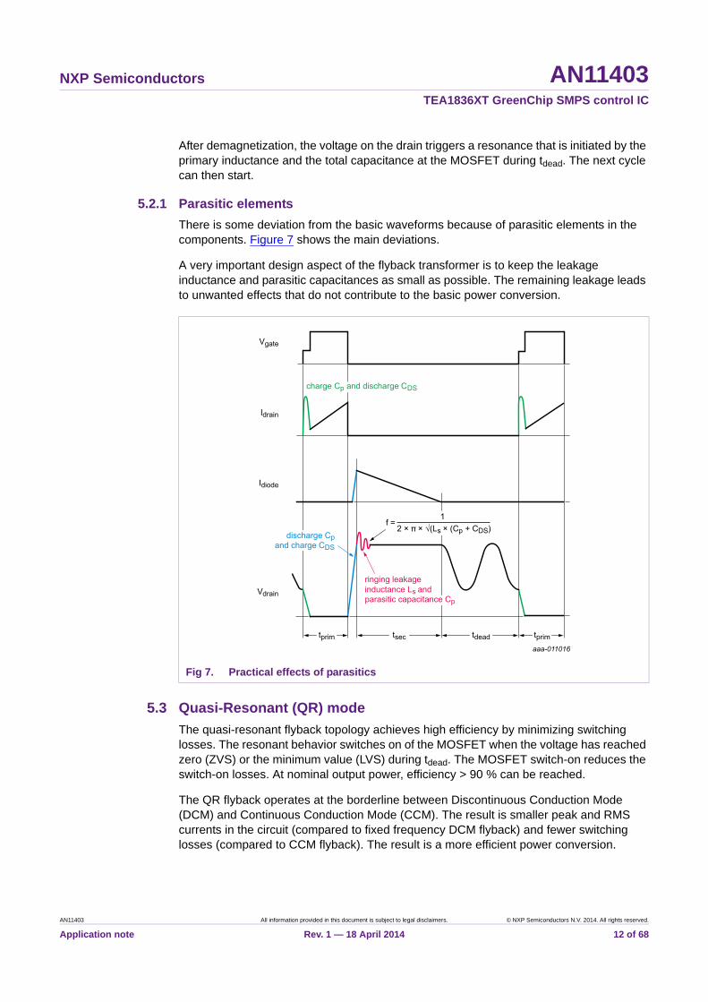
After demagnetization, the voltage on the drain triggers a resonance that is initiated by the primary inductance and the total capacitance at the MOSFET during tdead. The next cycle can then start.
5.2.1 Parasitic elements
There is some deviation from the basic waveforms because of parasitic elements in the components. Figure 7 shows the main deviations.
A very important design aspect of the flyback transformer is to keep the leakage inductance and parasitic capacitances as small as possible. The remaining leakage leads to unwanted effects that do not contribute to the basic power conversion.
5.3 Quasi-Resonant (QR) mode
The quasi-resonant flyback topology achieves high efficiency by minimizing switching losses. The resonant behavior switches on of the MOSFET when the voltage has reached zero (ZVS) or the minimum value (LVS) during tdead. The MOSFET switch-on reduces the switch-on losses. At nominal output power, efficiency > 90 % can be reached.
The QR flyback operates at the borderline between Discontinuous Conduction Mode (DCM) and Continuous Conduction Mode (CCM). The result is smaller peak and RMS currents in the circuit (compared to fixed frequency DCM flyback) and fewer switching losses (compared to CCM flyback). The result is a more efficient power conversion.
Fig 7. Practical effects of parasitics
AN11403 All information provided in this document is subject to legal disclaimers. © NXP Semiconductors N.V. 2014. All rights reserved.
Application note Rev. 1 — 18 April 2014 12 of 68
NXP Semiconductors AN11403TEA1836XT GreenChip SMPS control IC
The flyback topology is suitable for use as a single stage power supply in a universal mains voltage system. It can be implemented as single stage system in applications where no PFC function is required. Normally, these applications have a nominal power rating < 75 W.
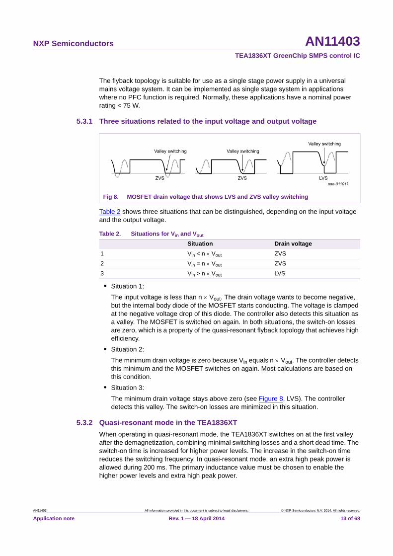
5.3.1 Three situations related to the input voltage and output voltage
Table 2 shows three situations that can be distinguished, depending on the input voltage and the output voltage.
• Situation 1:
The input voltage is less than n Vout. The drain voltage wants to become negative, but the internal body diode of the MOSFET starts conducting. The voltage is clamped at the negative voltage drop of this diode. The controller also detects this situation as a valley. The MOSFET is switched on again. In both situations, the switch-on losses are zero, which is a property of the quasi-resonant flyback topology that achieves high efficiency.
• Situation 2:
The minimum drain voltage is zero because Vin equals n Vout. The controller detects this minimum and the MOSFET switches on again. Most calculations are based on this condition.
• Situation 3:
The minimum drain voltage stays above zero (see Figure 8, LVS). The controller detects this valley. The switch-on losses are minimized in this situation.
5.3.2 Quasi-resonant mode in the TEA1836XT
When operating in quasi-resonant mode, the TEA1836XT switches on at the first valley after the demagnetization, combining minimal switching losses and a short dead time. The switch-on time is increased for higher power levels. The increase in the switch-on time reduces the switching frequency. In quasi-resonant mode, an extra high peak power is allowed during 200 ms. The primary inductance value must be chosen to enable the higher power levels and extra high peak power.
Fig 8. MOSFET drain voltage that shows LVS and ZVS valley switching
Table 2. Situations for Vin and Vout
Situation Drain voltage
1 Vin < n Vout ZVS
2 Vin = n Vout ZVS
3 Vin > n Vout LVS
AN11403 All information provided in this document is subject to legal disclaimers. © NXP Semiconductors N.V. 2014. All rights reserved.
Application note Rev. 1 — 18 April 2014 13 of 68
NXP Semiconductors AN11403TEA1836XT GreenChip SMPS control IC
5.4 Discontinuous Conduction Mode (DCM)
DCM is similar to the quasi-resonant mode except that there is more time without current flowing after the demagnetization has ended. This time is also called dead time.
5.4.1 DCM in the TEA1836XT
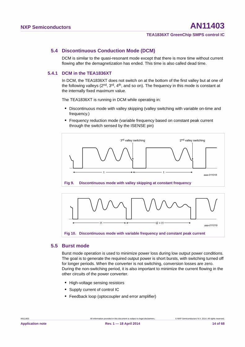
In DCM, the TEA1836XT does not switch on at the bottom of the first valley but at one of the following valleys (2nd, 3rd, 4th, and so on). The frequency in this mode is constant at the internally fixed maximum value.
The TEA1836XT is running in DCM while operating in:
• Discontinuous mode with valley skipping (valley switching with variable on-time and frequency.)
• Frequency reduction mode (variable frequency based on constant peak current through the switch sensed by the ISENSE pin)
5.5 Burst mode
Burst mode operation is used to minimize power loss during low output power conditions. The goal is to generate the required output power is short bursts, with switching turned off for longer periods. When the converter is not switching, conversion losses are zero. During the non-switching period, it is also important to minimize the current flowing in the other circuits of the power converter.
• High-voltage sensing resistors
• Supply current of control IC
• Feedback loop (optocoupler and error amplifier)
Fig 9. Discontinuous mode with valley skipping at constant frequency
Fig 10. Discontinuous mode with variable frequency and constant peak current
AN11403 All information provided in this document is subject to legal disclaimers. © NXP Semiconductors N.V. 2014. All rights reserved.
Application note Rev. 1 — 18 April 2014 14 of 68
NXP Semiconductors AN11403TEA1836XT GreenChip SMPS control IC
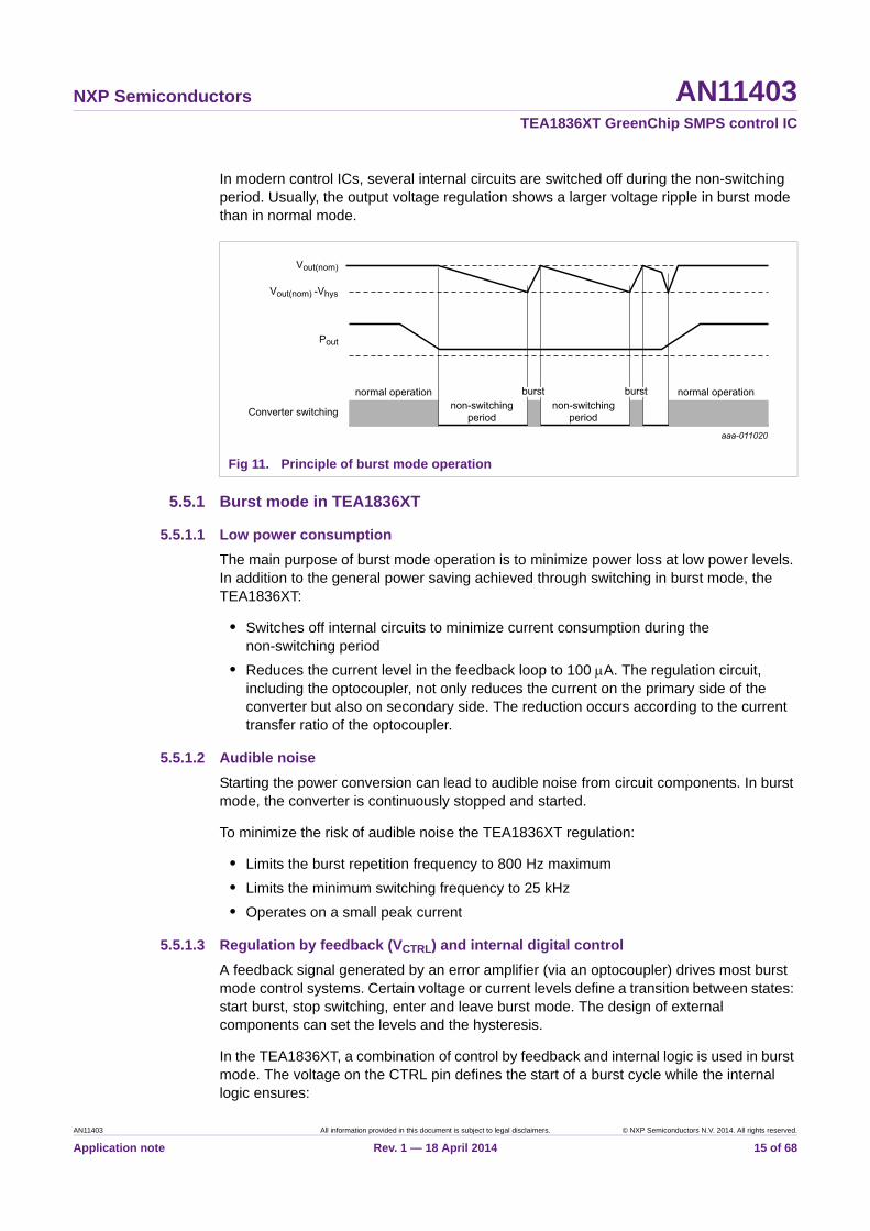
In modern control ICs, several internal circuits are switched off during the non-switching period. Usually, the output voltage regulation shows a larger voltage ripple in burst mode than in normal mode.
5.5.1 Burst mode in TEA1836XT
5.5.1.1 Low power consumption
The main purpose of burst mode operation is to minimize power loss at low power levels. In addition to the general power saving achieved through switching in burst mode, the TEA1836XT:
• Switches off internal circuits to minimize current consumption during the non-switching period
• Reduces the current level in the feedback loop to 100 A. The regulation circuit, including the optocoupler, not only reduces the current on the primary side of the converter but also on secondary side. The reduction occurs according to the current transfer ratio of the optocoupler.
5.5.1.2 Audible noise
Starting the power conversion can lead to audible noise from circuit components. In burst mode, the converter is continuously stopped and started.
To minimize the risk of audible noise the TEA1836XT regulation:
• Limits the burst repetition frequency to 800 Hz maximum
• Limits the minimum switching frequency to 25 kHz
• Operates on a small peak current
5.5.1.3 Regulation by feedback (VCTRL) and internal digital control
A feedback signal generated by an error amplifier (via an optocoupler) drives most burst mode control systems. Certain voltage or current levels define a transition between states: start burst, stop switching, enter and leave burst mode. The design of external components can set the levels and the hysteresis.
In the TEA1836XT, a combination of control by feedback and internal logic is used in burst mode. The voltage on the CTRL pin defines the start of a burst cycle while the internal logic ensures:
Fig 11. Principle of burst mode operation
AN11403 All information provided in this document is subject to legal disclaimers. © NXP Semiconductors N.V. 2014. All rights reserved.
Application note Rev. 1 — 18 April 2014 15 of 68
NXP Semiconductors AN11403TEA1836XT GreenChip SMPS control IC
• Limits of operation for audible noise (see Section 5.5.1.2)
• Fast load step response
• Low power consumption
The combination of two masters in control can sometimes lead to complex behavior when several control mechanisms are active at the same time.
6. Introduction to flyback converter design
For a quasi-resonant flyback converter, the output power (Po) can be calculated with Equation 1:
(1)
Where:
• Lp is the flyback transformer primary inductance
• Ipk(prim) is the flyback transformer primary peak current
• foper is the flyback controller operating frequency
• is the flyback converter efficiency
As the output power demand slowly increases, the converter passes through several control modes.
Converter design involves matching the transformer design to the system requirements. The extra high peak power capability is an additional feature of the TEA1836XT concept.
6.1 Converter design including OverPower Protection (OPP)
Choices made during the design of the converter must be compatible with the TEA1836XT system concept. Two additional protection functions (internal levels) must be included in the design considerations:
• Overpower protection (pin AUX)
• Overpower counter (pin ISENSE)
The maximum power the flyback converter can support depends on the input voltage. A higher input voltage allows for more output power, which can result in more stress during fault conditions. The OPP function is implemented to limit the output power to a predefined value.
Po12--- Lp Ipk prim foper =
AN11403 All information provided in this document is subject to legal disclaimers. © NXP Semiconductors N.V. 2014. All rights reserved.
Application note Rev. 1 — 18 April 2014 16 of 68

NXP Semiconductors AN11403TEA1836XT GreenChip SMPS control IC
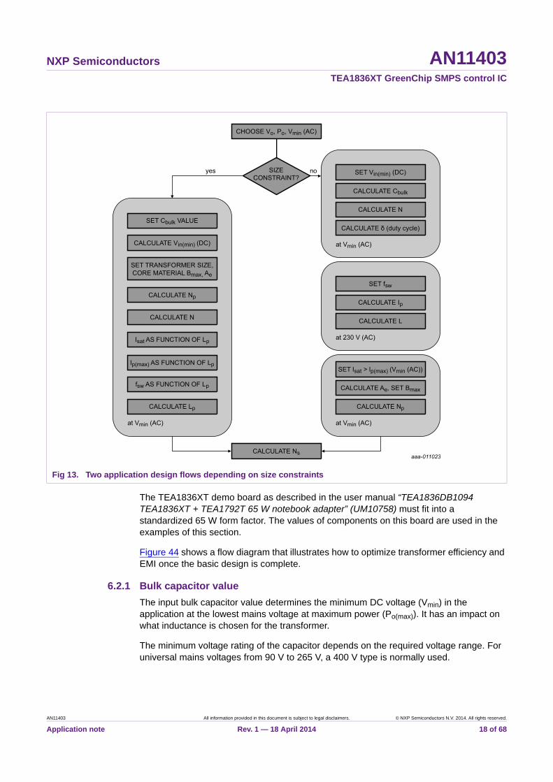
6.2 Transformer parameters design flow
In this section, a design flow is introduced to calculate the transformer parameters and component values in the application. Extended peak power (150 %) capability is one of the key features of the TEA1836XT. The entire application must be able to support this feature. It plays a dominant role in the decisions to be made.
Two design methods are presented, distinguished by possible design constraints regarding the application size. The calculations follow different orders in the two approaches and parameters (Ip, frequency) have different priorities.
Figure 13 shows the application design flow. Because a small-size application is often required, the left-side design flow is used as an example in this section. The right-side design flow is the traditional straightforward design method.
Fig 12. Overpower design considerations (with example values)
AN11403 All information provided in this document is subject to legal disclaimers. © NXP Semiconductors N.V. 2014. All rights reserved.
Application note Rev. 1 — 18 April 2014 17 of 68
NXP Semiconductors AN11403TEA1836XT GreenChip SMPS control IC
The TEA1836XT demo board as described in the user manual “TEA1836DB1094 TEA1836XT + TEA1792T 65 W notebook adapter” (UM10758) must fit into a standardized 65 W form factor. The values of components on this board are used in the examples of this section.
Figure 44 shows a flow diagram that illustrates how to optimize transformer efficiency and EMI once the basic design is complete.
6.2.1 Bulk capacitor value
The input bulk capacitor value determines the minimum DC voltage (Vmin) in the application at the lowest mains voltage at maximum power (Po(max)). It has an impact on what inductance is chosen for the transformer.
The minimum voltage rating of the capacitor depends on the required voltage range. For universal mains voltages from 90 V to 265 V, a 400 V type is normally used.
Fig 13. Two application design flows depending on size constraints
AN11403 All information provided in this document is subject to legal disclaimers. © NXP Semiconductors N.V. 2014. All rights reserved.
Application note Rev. 1 — 18 April 2014 18 of 68
NXP Semiconductors AN11403TEA1836XT GreenChip SMPS control IC
6.2.1.1 Demo board example
• The required maximum output power (Po(max)) for OPP is 150 % 65 W = 100 W
• The minimum mains voltage (Vmains(min)) is 90 V (AC)
• The frequency at minimum mains voltage is 60 Hz
• The expected efficiency is approximately 90 %
The relationship between bulk capacitor value and lowest DC voltage can be calculated with Equation 2:
(2)
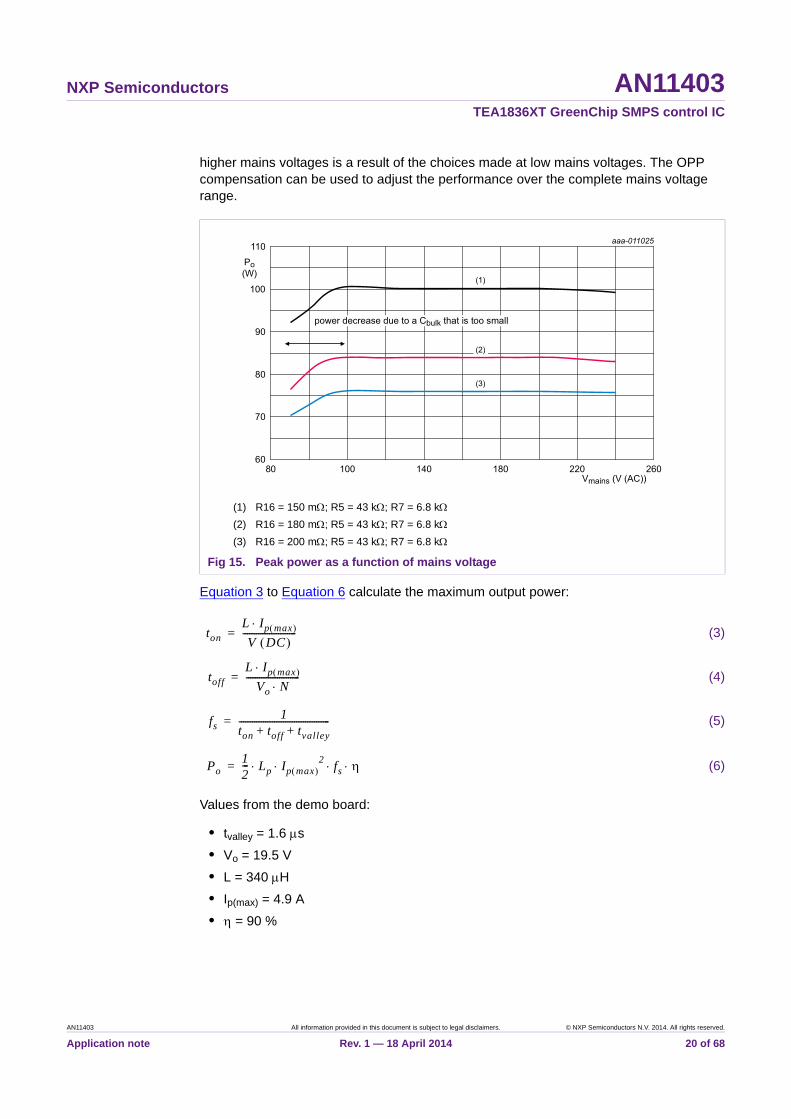
Target for the minimum bulk voltage is set to be approximately 75 V (DC) to avoid large ton times and very low switching frequencies. Taking into account 20 % for aging and tolerance, the bulk capacitor value must be > 150 F to fulfill this requirement. In the demo board, 120 F is used to fit the application in a standardized 65 W form factor.
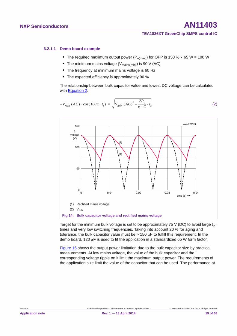
Figure 15 shows the output power limitation due to the bulk capacitor size by practical measurements. At low mains voltage, the value of the bulk capacitor and the corresponding voltage ripple on it limit the maximum output power. The requirements of the application size limit the value of the capacitor that can be used. The performance at
(1) Rectified mains voltage
(2) Vbulk
Fig 14. Bulk capacitor voltage and rectified mains voltage
V– min AC 100 ts cos Vmin AC 22Po
C------------ ts–=
AN11403 All information provided in this document is subject to legal disclaimers. © NXP Semiconductors N.V. 2014. All rights reserved.
Application note Rev. 1 — 18 April 2014 19 of 68
NXP Semiconductors AN11403TEA1836XT GreenChip SMPS control IC
higher mains voltages is a result of the choices made at low mains voltages. The OPP compensation can be used to adjust the performance over the complete mains voltage range.
Equation 3 to Equation 6 calculate the maximum output power:
(3)
(4)
(5)
(6)
Values from the demo board:
• tvalley = 1.6 s
• Vo = 19.5 V
• L = 340 H
• Ip(max) = 4.9 A
• = 90 %
(1) R16 = 150 m; R5 = 43 k; R7 = 6.8 k
(2) R16 = 180 m; R5 = 43 k; R7 = 6.8 k
(3) R16 = 200 m; R5 = 43 k; R7 = 6.8 k
Fig 15. Peak power as a function of mains voltage
ton
L Ip max V DC
------------------------=
toff
L Ip max Vo N
------------------------=
fs1
ton toff tvalley+ +-----------------------------------------=
Po12--- Lp Ip max
2fs =
AN11403 All information provided in this document is subject to legal disclaimers. © NXP Semiconductors N.V. 2014. All rights reserved.
Application note Rev. 1 — 18 April 2014 20 of 68
NXP Semiconductors AN11403TEA1836XT GreenChip SMPS control IC
6.2.2 Transformer saturation margin at maximum peak power
Generally, transformer saturation is generally avoided to obtain a reliable and predictable performance of the power supply including production spread, aging and temperature. In certain cases, such as high peak power capability, there can be reasons for allowing some risk of saturation under extreme operating conditions. Possible reasons for this include:
• The peak power duration is expected to be short (200 ms is the maximum allowed overpower time).
• In practice, the application operates at a nominal mains input voltage (for example 115 V (AC)). It relaxes the operating conditions regarding the lowest mains input voltage at which the application can operate. When a margin for saturation is required for all cases, the transformer size increases significantly. The result is a commercially less attractive application solution.
It is important to decide what strategy must be followed concerning margin to saturation.
6.2.3 Relationship between transformer saturation current and inductance
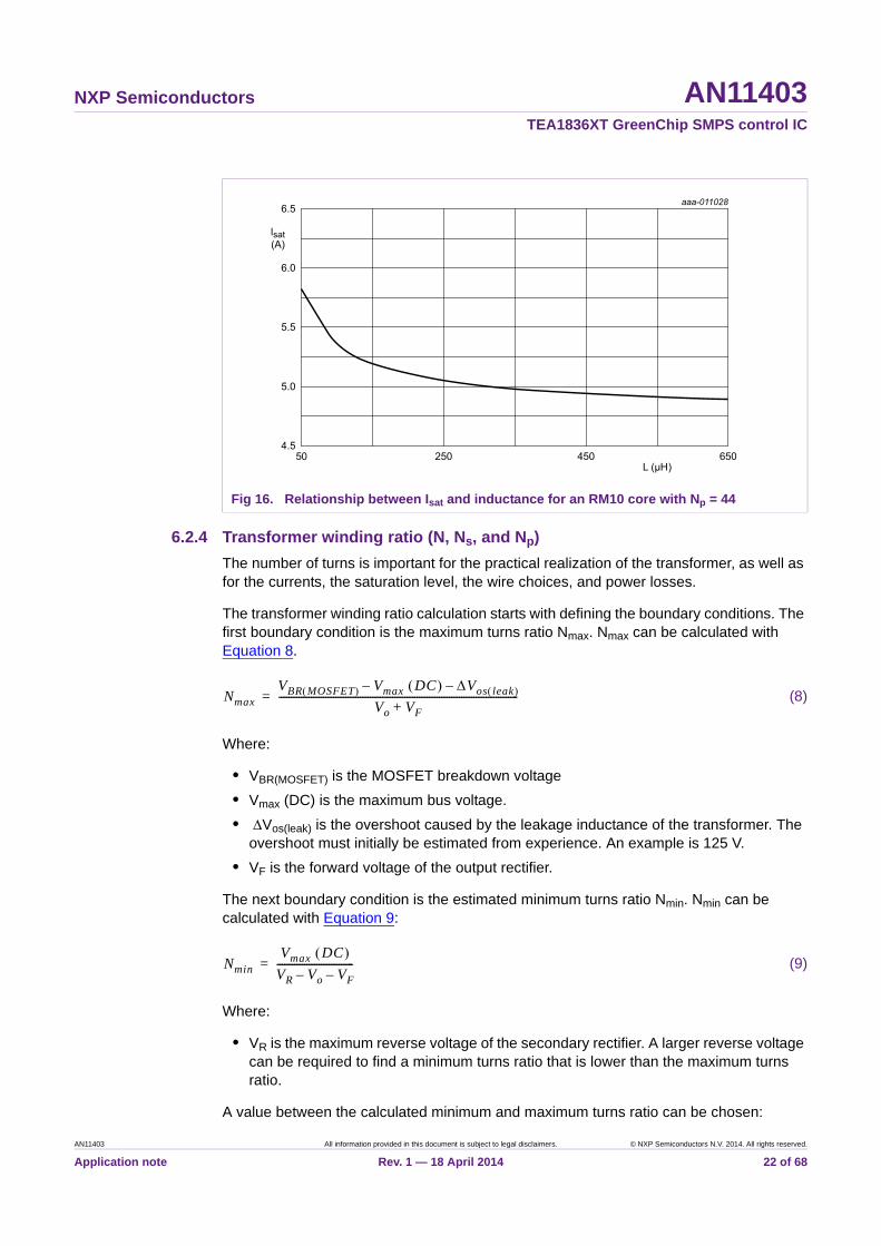
In some cases (like in the TEA1836DB1094 demo board (UM10758)), a specific form factor is requested for the application. This specific form factor dictates the transformer size.
When the transformer size and the core material type are known, the relationship between inductance and saturation current can be calculated with Equation 7:
(7)
Where for an RM10 core:
• Bmax (magnetic flux density) = 0.38 T (at 25 C)
• Ae (effective area (m2)) = 09.66 105 m2
Remark: Bmax decreases when the temperature rises.
When the wire thickness is selected, the number of windings that fit on the bobbin can be calculated. For the TEA1836DB1094 demo board (UM10758) the number of windings is 2 times 22:
• Np = 44
Figure 16 shows the relationship between Ip(sat) and inductance Lp.
Ip sat Np Bmax Ae
Lp-------------------------------------=
AN11403 All information provided in this document is subject to legal disclaimers. © NXP Semiconductors N.V. 2014. All rights reserved.
Application note Rev. 1 — 18 April 2014 21 of 68
NXP Semiconductors AN11403TEA1836XT GreenChip SMPS control IC
6.2.4 Transformer winding ratio (N, Ns, and Np)
The number of turns is important for the practical realization of the transformer, as well as for the currents, the saturation level, the wire choices, and power losses.
The transformer winding ratio calculation starts with defining the boundary conditions. The first boundary condition is the maximum turns ratio Nmax. Nmax can be calculated with Equation 8.
(8)
Where:
• VBR(MOSFET) is the MOSFET breakdown voltage
• Vmax (DC) is the maximum bus voltage.
• Vos(leak) is the overshoot caused by the leakage inductance of the transformer. The overshoot must initially be estimated from experience. An example is 125 V.
• VF is the forward voltage of the output rectifier.
The next boundary condition is the estimated minimum turns ratio Nmin. Nmin can be calculated with Equation 9:
(9)
Where:
• VR is the maximum reverse voltage of the secondary rectifier. A larger reverse voltage can be required to find a minimum turns ratio that is lower than the maximum turns ratio.
A value between the calculated minimum and maximum turns ratio can be chosen:
Fig 16. Relationship between Isat and inductance for an RM10 core with Np = 44
Nmax
VBR MOSFET Vmax DC Vos leak ––
Vo VF+-------------------------------------------------------------------------------------------------=
Nmin
Vmax DC VR Vo VF––-------------------------------=
AN11403 All information provided in this document is subject to legal disclaimers. © NXP Semiconductors N.V. 2014. All rights reserved.
Application note Rev. 1 — 18 April 2014 22 of 68
NXP Semiconductors AN11403TEA1836XT GreenChip SMPS control IC
For a universal mains notebook adapter with 19.5 V output voltage, the boundaries give plenty of room for optimization. A reflected output voltage N Vo of approximately 100 V is a good starting point for the design to reach an acceptable maximum peak voltage on the primary MOSFET (see Figure 6).
The relationship between Np, Ns, and N can be calculated with Equation 10:
(10)
The flyback transformer is dimensioned for an optimal LVS/ZVS benefit. The reflected voltage N Vo must be as high as possible to force the lowest possible drain voltage when the MOSFET is switched on. For a low output voltage application, the turns ratio N = Np / Ns must be substantially increased to achieve the lowest possible drain voltage at MOSFET switch-on.
6.2.5 Relationship between maximum peak current and inductance
The maximum peak current must be lower than the expected saturation current. The selected margin between the two defines the inductance.
The maximum peak current as a function of the inductance can be calculated with Equation 11:
(11)
Where:
•
•
•
Figure 17 shows the relationship between Ip(max) and inductance Lp.
Nmin N Nmax
NNp
Ns------ 44
8------ 5.5= = =
Ip max b– b
24 a c–+
2 a--------------------------------------------------=
a N Vin min DC Lp=
b 2– IO Lp N VO VF+ Vin min DC + =
c 2– IO tvalley N Vin min DC VO VF+ =
AN11403 All information provided in this document is subject to legal disclaimers. © NXP Semiconductors N.V. 2014. All rights reserved.
Application note Rev. 1 — 18 April 2014 23 of 68
NXP Semiconductors AN11403TEA1836XT GreenChip SMPS control IC
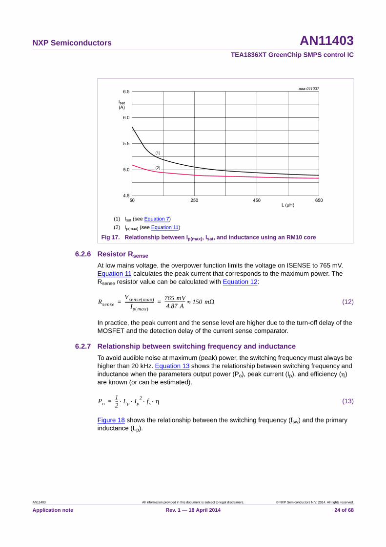
6.2.6 Resistor Rsense
At low mains voltage, the overpower function limits the voltage on ISENSE to 765 mV. Equation 11 calculates the peak current that corresponds to the maximum power. The Rsense resistor value can be calculated with Equation 12:
(12)
In practice, the peak current and the sense level are higher due to the turn-off delay of the MOSFET and the detection delay of the current sense comparator.
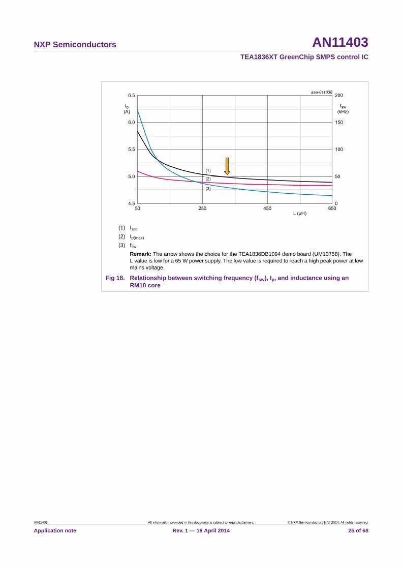
6.2.7 Relationship between switching frequency and inductance
To avoid audible noise at maximum (peak) power, the switching frequency must always be higher than 20 kHz. Equation 13 shows the relationship between switching frequency and inductance when the parameters output power (Po), peak current (Ip), and efficiency () are known (or can be estimated).
(13)
Figure 18 shows the relationship between the switching frequency (fsw) and the primary inductance (Lp).
(1) Isat (see Equation 7)
(2) Ip(max) (see Equation 11)
Fig 17. Relationship between Ip(max), Isat, and inductance using an RM10 core
Rsense
Vsense max
Ip max ---------------------------
765 mV4.87 A------------------- 150 m= =
Po12--- Lp Ip
2fs =
AN11403 All information provided in this document is subject to legal disclaimers. © NXP Semiconductors N.V. 2014. All rights reserved.
Application note Rev. 1 — 18 April 2014 24 of 68
NXP Semiconductors AN11403TEA1836XT GreenChip SMPS control IC
(1) Isat
(2) Ip(max)
(3) fsw
Remark: The arrow shows the choice for the TEA1836DB1094 demo board (UM10758). The L value is low for a 65 W power supply. The low value is required to reach a high peak power at low mains voltage.
Fig 18. Relationship between switching frequency (fsw), Ip, and inductance using an RM10 core
AN11403 All information provided in this document is subject to legal disclaimers. © NXP Semiconductors N.V. 2014. All rights reserved.
Application note Rev. 1 — 18 April 2014 25 of 68
NXP Semiconductors AN11403TEA1836XT GreenChip SMPS control IC
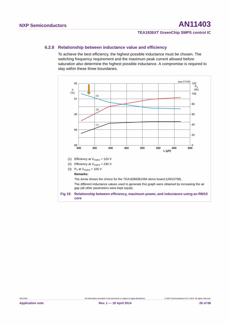
6.2.8 Relationship between inductance value and efficiency
To achieve the best efficiency, the highest possible inductance must be chosen. The switching frequency requirement and the maximum peak current allowed before saturation also determine the highest possible inductance. A compromise is required to stay within these three boundaries.
(1) Efficiency at Vmains = 120 V
(2) Efficiency at Vmains = 230 V
(3) Po at Vmains = 100 V
Remarks:
The arrow shows the choice for the TEA1836DB1094 demo board (UM10758).
The different inductance values used to generate this graph were obtained by increasing the air gap (all other parameters were kept equal).
Fig 19. Relationship between efficiency, maximum power, and inductance using an RM10 core
AN11403 All information provided in this document is subject to legal disclaimers. © NXP Semiconductors N.V. 2014. All rights reserved.
Application note Rev. 1 — 18 April 2014 26 of 68
NXP Semiconductors AN11403TEA1836XT GreenChip SMPS control IC
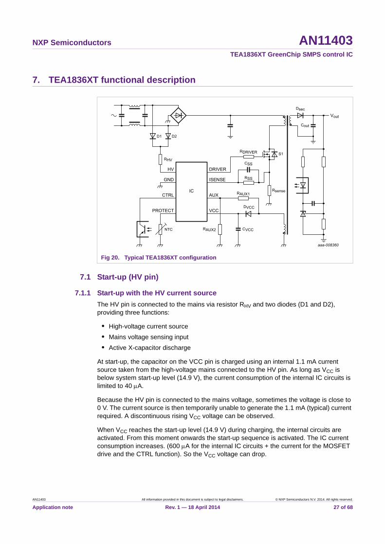
7. TEA1836XT functional description
7.1 Start-up (HV pin)
7.1.1 Start-up with the HV current source
The HV pin is connected to the mains via resistor RHV and two diodes (D1 and D2), providing three functions:
• High-voltage current source
• Mains voltage sensing input
• Active X-capacitor discharge
At start-up, the capacitor on the VCC pin is charged using an internal 1.1 mA current source taken from the high-voltage mains connected to the HV pin. As long as VCC is below system start-up level (14.9 V), the current consumption of the internal IC circuits is limited to 40 A.
Because the HV pin is connected to the mains voltage, sometimes the voltage is close to 0 V. The current source is then temporarily unable to generate the 1.1 mA (typical) current required. A discontinuous rising VCC voltage can be observed.
When VCC reaches the start-up level (14.9 V) during charging, the internal circuits are activated. From this moment onwards the start-up sequence is activated. The IC current consumption increases. (600 A for the internal IC circuits + the current for the MOSFET drive and the CTRL function). So the VCC voltage can drop.
Fig 20. Typical TEA1836XT configuration
AN11403 All information provided in this document is subject to legal disclaimers. © NXP Semiconductors N.V. 2014. All rights reserved.
Application note Rev. 1 — 18 April 2014 27 of 68

NXP Semiconductors AN11403TEA1836XT GreenChip SMPS control IC
When the converter starts, an auxiliary winding on the transformer generates the supply voltage for the VCC pin. Although the internal HV current source cannot generate all the energy required to operate the IC during start-up, it remains active. The HV current source stops when the voltage on the CTRL pin drops to below 5 V. The voltage drop indicates that the converter output voltage is close to nominal and start-up is complete.
The value of the VCC capacitor is minimized by extending the HV current source operation until the end of the start-up period.
7.1.2 Start-up sequence
When the VCC pin is charged to the 14.9 V start-up level, the IC continues with the start-up sequence.
• The PROTECT pin is charged to 0.55 V (detection voltage (0.5 V) + hysteresis voltage (0.05 V)).
• The mains voltage must exceed the brownin level (663 A at the HV pin).
• The CTRL pin is charged. It must reach the 5 V start-up level.
• The voltage on the VCC pin > 14.9 V
When these conditions are met, the soft start capacitor on the ISENSE pin (CSS in Figure 20) is charged. The system starts switching. In a typical application, the auxiliary winding of the transformer takes over the supply voltage.
If the start-up conditions are not met, the VCC voltage can drop due to the increased current consumption of the IC (full operation). Charging the VCC pin to the full 14.9 V again after the start conditions have been met avoids an unwanted restart during the start-up sequence because of VCC reaching the restart level. It ensures a defined VCC hysteresis (Vstart Vuvlo) during the start-up period. A restart during start-up leads to a non-monotonic rising of the output voltage.
AN11403 All information provided in this document is subject to legal disclaimers. © NXP Semiconductors N.V. 2014. All rights reserved.
Application note Rev. 1 — 18 April 2014 28 of 68

NXP Semiconductors AN11403TEA1836XT GreenChip SMPS control IC
7.1.3 Soft start
During start-up, the ISENSE function performs a soft start sequence. The soft start minimizes the risk of audible noise at start-up.
For this sequence, an internal current source of 75 A charges the external soft start capacitor. When the voltage on the ISENSE pin reaches 765 mV, the current source is switched off. The controller starts switching. The soft start capacitor slowly discharges via the soft start resistor that is connected in parallel.
The voltage level on ISENSE pin is measured constantly. Peak current is limited by switching off the MOSFET when the voltage reaches Vopp(ISENSE) (= 500 mV).
Fig 21. Start-up sequence
AN11403 All information provided in this document is subject to legal disclaimers. © NXP Semiconductors N.V. 2014. All rights reserved.
Application note Rev. 1 — 18 April 2014 29 of 68

NXP Semiconductors AN11403TEA1836XT GreenChip SMPS control IC
While the voltage drop on the ISENSE pin is falling from 765 mV (start-up level) to Vopp(ISENSE), the DRIVER pulses are short because the voltage already exceeds the limiting Vopp(ISENSE) level when the driver is activated. An internal timer of 665 ns limits the on-time during this period.
As the voltage offset decreases due to the discharging of CSS, the peak current slowly increases. When the voltage on the CTRL pin drops to 5 V, start-up ends. Voltage sensing and regulation by ISENSE then operate normally.
The capacitor value and the value of the parallel resistor can set the soft start time.
To ensure that the internal current source including tolerances can reach the start level, the RSS value must exceed 12 k.
To prevent that negative spikes reach the pin, capacitor CSS and resistor RSS must be placed close to the IC. The internal ESD protection diode rectifies the negative spikes which cause a DC offset. A resistor (for example 1 k) in series with the connection to the ISENSE pin can also help to reduce disturbance. The series resistor shows a small voltage drop when the 75 A current source is stopped (Vsense(max) = 765 mV). The voltage drop causes no problems because the limiting value of the peak current on the ISENSE pin during soft start is lower (same level for the OPP function: 295 mV < Vopp(ISENSE) < 500 mV).
7.2 Modes of operation
7.2.1 Feedback control (CTRL pin)
Feedback control incorporates two systems:
• An analog controlled normal mode
• An analog/digital controlled burst mode
The voltage on the CTRL pin determines the power level. However, during burst mode, the current value can also determine when the switching of the burst ends.
Three different ranges can be distinguished in the voltage on the CTRL pin:
• Ipeak control in QR mode (2.5 V < VCTRL < 5.35 V)
• Frequency control (0.5 V < CTRL < 2.5 V) with a constant peak current (VISENSE = 207 mV)
• Burst mode operation (CTRL < 0.5 V)
The switching frequency is monitored and limited to 125 kHz.
RSS CSS=
AN11403 All information provided in this document is subject to legal disclaimers. © NXP Semiconductors N.V. 2014. All rights reserved.
Application note Rev. 1 — 18 April 2014 30 of 68
NXP Semiconductors AN11403TEA1836XT GreenChip SMPS control IC
The voltage on the CRTL pin is obtained by pulling current out of the pin. Normally, an error amplifier using an optocoupler in the regulation loop pulls the current.
In normal mode (0.5 V < CTRL), an 11.2 k internal pull-up resistor connected to a fixed internal source of 7 V generates this current.
The internal voltage source shows a 7 V value during operation when some current is taken from it. At start-up, the current is zero. At zero current, the internal voltage source is not in regulation and clamps to its own approximately 10 V input voltage. In this situation, the CTRL voltage also changes to approximately 10 V.
7.2.2 Normal mode operation
At start-up or restart, an internal source pulls up the voltage on the pin to approximately 10 V before switching is started. When switching starts, the supply to the CTRL pin is internally connected to a 7 V source using an 11.2 k series resistor. When the control loop becomes active, it pulls current from the CTRL pin. Because of the internal resistor of 11.2 k, the voltage on CTRL drops to the correct power level. This resulting voltage on the CTRL pin is the input for the regulation (see Figure 22).
When, because of a fault condition, the CTRL pin cannot reach the start-up level of 5 V, switching does not start. The IC restarts because VCC drops to the restart voltage.
When the 5 V start-up level is reached, start-up continues by charging via Isense, so a soft start can be realized.
The 2.5 V level divides the normal mode control range into two modes.
• Frequency reduction
• Peak current control
Below 0.5 V the IC enters burst mode.
Fig 22. Feedback control
AN11403 All information provided in this document is subject to legal disclaimers. © NXP Semiconductors N.V. 2014. All rights reserved.
Application note Rev. 1 — 18 April 2014 31 of 68

NXP Semiconductors AN11403TEA1836XT GreenChip SMPS control IC
Using peak current control, the switching frequency at higher power in quasi-resonant mode is determined by the regulation. When, at lower output power in this mode, the frequency increases, it is limited to 132.5 kHz until the regulation reaches the frequency reduction mode (VCTRL = 2.5 V). The limitation is achieved through valley skipping.
In frequency reduction mode, the peak current is kept constant (VISENSE = 207 mV). When, at lower output power in this mode, the frequency decreases, it is limited to 25 kHz until the regulation reaches the burst mode at VCTRL = 0.5 V. During burst mode, the voltage on the CTRL pin is clamped. The switching frequency remains 25 kHz limiting the risk of audible noise.
Fig 23. Modes of operation including frequency limiting
AN11403 All information provided in this document is subject to legal disclaimers. © NXP Semiconductors N.V. 2014. All rights reserved.
Application note Rev. 1 — 18 April 2014 32 of 68
NXP Semiconductors AN11403TEA1836XT GreenChip SMPS control IC
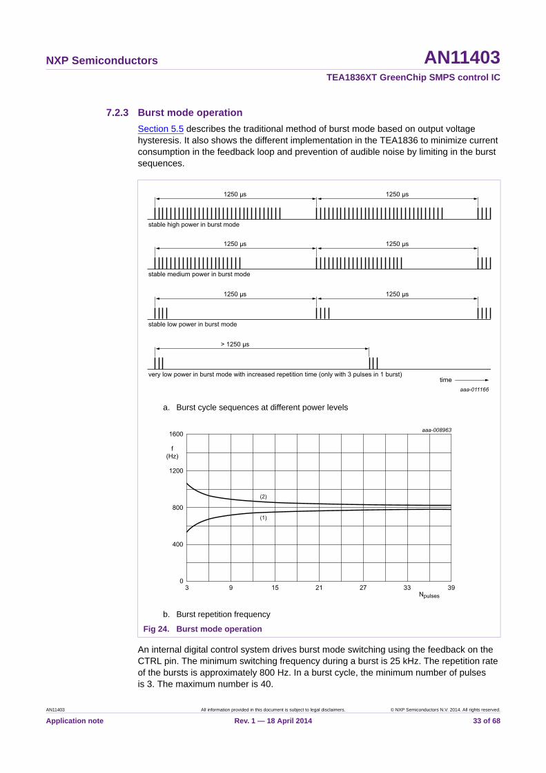
7.2.3 Burst mode operation
Section 5.5 describes the traditional method of burst mode based on output voltage hysteresis. It also shows the different implementation in the TEA1836 to minimize current consumption in the feedback loop and prevention of audible noise by limiting in the burst sequences.
An internal digital control system drives burst mode switching using the feedback on the CTRL pin. The minimum switching frequency during a burst is 25 kHz. The repetition rate of the bursts is approximately 800 Hz. In a burst cycle, the minimum number of pulses is 3. The maximum number is 40.
a. Burst cycle sequences at different power levels
b. Burst repetition frequency
Fig 24. Burst mode operation
AN11403 All information provided in this document is subject to legal disclaimers. © NXP Semiconductors N.V. 2014. All rights reserved.
Application note Rev. 1 — 18 April 2014 33 of 68

NXP Semiconductors AN11403TEA1836XT GreenChip SMPS control IC
In burst mode operation (VCTRL < 0.5 V), an internal variable voltage source regulates a 100 mA current source, reducing the power consumption by the optocoupler feedback circuit.
During each burst, a clamp circuit is activated to clamp the CTRL voltage to the minimum level of 0.5 V. The current pulled from the CTRL pin by the control loop (using an optocoupler) is measured for switching control (detecting a sudden output voltage rise or drop). The clamping to 0.5 V is done to increase the optocoupler current measurement accuracy in burst mode (100 A < Iopto < 750 A). Even if the target number of pulses has not been reached yet, the switching stops when the current exceeds 750 A (100 A plus an internal additional current reference). Stopping the switching avoids the increase of the output voltage when the load demand drops suddenly. Switching during a burst continues when the current drops to 90 A.
To ensure an equal starting point for each burst cycle, the CTRL voltage is pulled low after each burst cycle.
To ensure a consistent history-independent behavior in normal mode, the internal CTRL supply voltage is regulated slowly to 7 V when the IC leaves burst mode.
To reduce the IC current consumption to 235 A, internal circuits that are not essential are switched off during the non-switching periods.
7.2.3.1 Primary peak current during a burst
During a burst, the peak current through the primary MOSFET and the switching frequency can vary according to the normal regulation. This variation ensures a smooth transition between burst mode and normal mode. However, the frequency must not drop to below 25 kHz.
Fig 25. CTRL circuit for normal mode and burst mode
AN11403 All information provided in this document is subject to legal disclaimers. © NXP Semiconductors N.V. 2014. All rights reserved.
Application note Rev. 1 — 18 April 2014 34 of 68
NXP Semiconductors AN11403TEA1836XT GreenChip SMPS control IC
7.2.3.2 The burst sequence and target number of pulses
Each burst starts when the voltage on the CTRL pin reaches 0.5 V. When 0.5 V is reached, the circuit is activated to generate a burst.
Depending on the requested power, the number of pulses remains constant, increases, or decreases gradually from burst to burst. Based on the duration of the burst time + waiting time, the internal algorithm calculates the number of pulses for the next cycle.
• When the voltage on the CTRL pin exceeds 0.5 V before 1250 s (800 Hz target) have passed from the start of the previous burst, an increased demand for power is detected. The number of pulses increases.
• When the voltage on the CTRL pin exceeds 0.5 V after 1250 s have passed from the start of the previous burst, a decreased demand for power is detected. The number of pulses decreases.
This mechanism regulates the burst repetition frequency to the target of 800 Hz.
When burst mode runs at only a few pulses per cycle, some deviation from the 800 Hz target is possible because the internal calculation is rounded off.
The basic algorithm for determining the number of pulses for the next cycle (ni+1) is:
(14)
The algorithm results in the following behavior: When increasing the number of switching cycles in one burst, the target is 2 times the previous number. When decreasing, the target is 0.5 times the previous number. In this way, the power is increased or decreased gradually.
When a new burst exceeds 40 pulses, the system enters normal mode. When the minimum of 3 pulses in a burst at 800 Hz repetition still generates too much power, the feedback loop increases the repetition time to the correct level. The repetition frequency is reduced to < 800 Hz.
Because the burst mode algorithm internally takes care of parameters such as the burst repetition rate, there is great freedom to adjust the application control loop components for optimal application performance.
7.2.3.3 Sensing for a load step requesting more power (ICTRL < 90 A)
A burst is started when the voltage on the CTRL pin exceeds 0.5 V. The CTRL current is sensed during the burst. Normally, the current source driven CTRL pin provides 100 A. When the CTRL current sensing circuit senses 100 A or more at the end of the burst sequence, the burst is ended. The output load is stable.
When the measured current at the end of a burst sequence is < 90 A, the feedback optocoupler requests more power because of an increased output load. In this case, the burst is not stopped but continued with a higher number of pulses. The burst continues until either the total number of pulses exceeds 40 and normal mode is entered or at the end of the sequence the CTRL current is 100 A or higher and the burst is ended.
ni 1+ ni12---
12--- 1250 s
ti period --------------------+
=
AN11403 All information provided in this document is subject to legal disclaimers. © NXP Semiconductors N.V. 2014. All rights reserved.
Application note Rev. 1 — 18 April 2014 35 of 68
NXP Semiconductors AN11403TEA1836XT GreenChip SMPS control IC
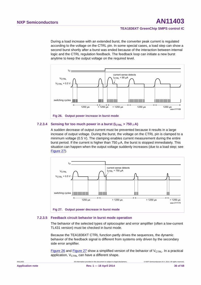
During a load increase with an extended burst, the converter peak current is regulated according to the voltage on the CTRL pin. In some special cases, a load step can show a second burst shortly after a burst was ended because of the interaction between internal logic and the CTRL regulation feedback. The feedback loop can initiate a new burst anytime to keep the output voltage on the required level.
7.2.3.4 Sensing for too much power in a burst (ICTRL > 750 A)
A sudden decrease of output current must be prevented because it results in a large increase of output voltage. During the burst, the voltage on the CTRL pin is clamped to a minimum voltage (0.5 V). The clamping enables current measurement during the entire burst period. If the current is higher than 750 A, the burst is stopped immediately. This situation can happen when the output voltage suddenly increases (due to a load step; see Figure 27).
7.2.3.5 Feedback circuit behavior in burst mode operation
The behavior of the selected types of optocoupler and error amplifier (often a low-current TL431 version) must be checked in burst mode.
Because the TEA1836XT CTRL function partly drives the sequences, the dynamic behavior of the feedback signal is different from systems only driven by the secondary side error amplifier.
Figure 26 and Figure 27 show a simplified version of the behavior of VCTRL. In a practical application, VCTRL can have a different shape.
Fig 26. Output power increase in burst mode
Fig 27. Output power decrease in burst mode
AN11403 All information provided in this document is subject to legal disclaimers. © NXP Semiconductors N.V. 2014. All rights reserved.
Application note Rev. 1 — 18 April 2014 36 of 68
NXP Semiconductors AN11403TEA1836XT GreenChip SMPS control IC
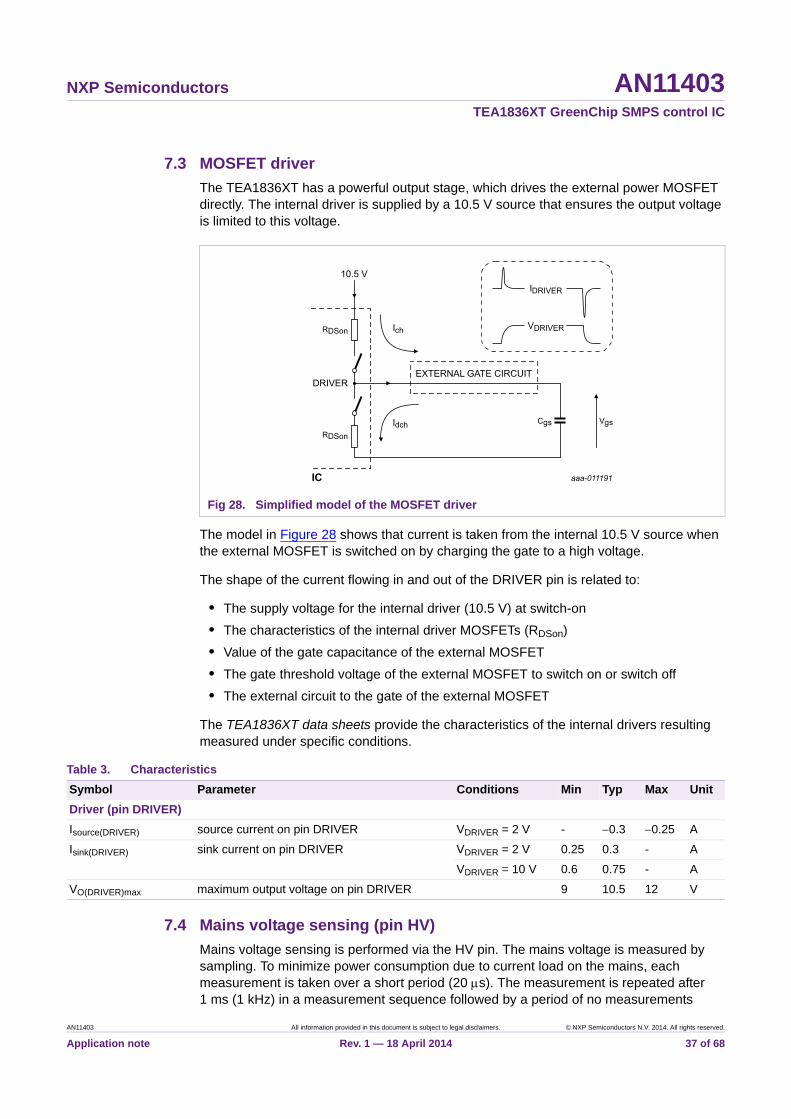
7.3 MOSFET driver
The TEA1836XT has a powerful output stage, which drives the external power MOSFET directly. The internal driver is supplied by a 10.5 V source that ensures the output voltage is limited to this voltage.
The model in Figure 28 shows that current is taken from the internal 10.5 V source when the external MOSFET is switched on by charging the gate to a high voltage.
The shape of the current flowing in and out of the DRIVER pin is related to:
• The supply voltage for the internal driver (10.5 V) at switch-on
• The characteristics of the internal driver MOSFETs (RDSon)
• Value of the gate capacitance of the external MOSFET
• The gate threshold voltage of the external MOSFET to switch on or switch off
• The external circuit to the gate of the external MOSFET
The TEA1836XT data sheets provide the characteristics of the internal drivers resulting measured under specific conditions.
7.4 Mains voltage sensing (pin HV)
Mains voltage sensing is performed via the HV pin. The mains voltage is measured by sampling. To minimize power consumption due to current load on the mains, each measurement is taken over a short period (20 s). The measurement is repeated after 1 ms (1 kHz) in a measurement sequence followed by a period of no measurements
Fig 28. Simplified model of the MOSFET driver
Table 3. Characteristics
Symbol Parameter Conditions Min Typ Max Unit
Driver (pin DRIVER)
Isource(DRIVER) source current on pin DRIVER VDRIVER = 2 V - 0.3 0.25 A
Isink(DRIVER) sink current on pin DRIVER VDRIVER = 2 V 0.25 0.3 - A
VDRIVER = 10 V 0.6 0.75 - A
VO(DRIVER)max maximum output voltage on pin DRIVER 9 10.5 12 V
AN11403 All information provided in this document is subject to legal disclaimers. © NXP Semiconductors N.V. 2014. All rights reserved.
Application note Rev. 1 — 18 April 2014 37 of 68

NXP Semiconductors AN11403TEA1836XT GreenChip SMPS control IC
(again to minimize power consumption). In burst mode, the period when no measurements are taken is longer (97 ms) than during normal operation (6 ms). This longer period is called wait time.
Measurement are taken during the sampling period by switching the HV pin to ground level and measuring the current that flows from the mains through the series resistor at the end of the 20 s period. The internal circuit that connects the HV pin to ground and measures the current introduces a voltage drop of approximately 2.6 V. So, during this sampling period, a voltage of 2.6 V can be observed on the HV pin.
7.4.1 Mains sense circuit
Two diodes connected from the mains to the HV pin using a 130 k series resistor provide the basic mains sensing circuit. Figure 29 shows two extra 50 k resistors in series with the diodes. These resistors prevent a potentially unsafe situation occurring if one diode fails and remains as a short circuit. In this situation, the two 50 k resistors limit the power in the remaining circuit between the two mains connections.
7.4.2 Brownin
When the VCC is charged to the start level, mains sensing is activated to generate one of the required conditions for starting the converter. The mains voltage is sensed in the normal sequence of three pulses and a wait time of 6 ms. When one pulse shows a value above the brownin value (663 A), converter start-up is enabled (as far as meeting the brownin requirements is concerned). Sensing continues after start-up.
Fig 29. Mains voltage sensing
AN11403 All information provided in this document is subject to legal disclaimers. © NXP Semiconductors N.V. 2014. All rights reserved.
Application note Rev. 1 — 18 April 2014 38 of 68
NXP Semiconductors AN11403TEA1836XT GreenChip SMPS control IC
In practice, the moment of sensing gradually synchronizes with the mains frequency around the low voltage parts, saving power consumption. The 6 ms wait time has been chosen to obtain this behavior, assuming a mains voltage frequency of 50 Hz or 60 Hz. There is no internal system regulating this behavior.
The brownin level can be calculated with Equation 15:
(15)
Example:
• Ibi(HV) = 663 A
• Vmeas(HV) = 2.6 V
• The required brownin level: Vmains (RMS) = 86 V
The result:
7.4.3 Brownout
If the mains voltage remains below the brownout level for at least 30 ms, a brownout is detected. The system stops switching. This delay period is built in to ensure that the system does not stop switching due to the zero crossings of the mains or during a short mains interruption.
The brownout level can be calculated with Equation 16:
(16)
Example:
• Ibo(HV) = 587 A
• Vmeas(HV) = 2.6 V
• The required brownout level: Vmains (RMS) = 76.5 V
The result:
The selection of a value for the HV pin series resistor determines both the brownin and the brownout value.
RHV
2 Vmains RMS Vmeas HV –Ibi HV
-------------------------------------------------------------------------------=
RHV2 86 2.6–
0.663--------------------------------- 180 k= =
RHV
2 Vmains RMS Vmeas HV –Ibo HV
-------------------------------------------------------------------------------=
RHV2 76.5 2.6–
0.587----------------------------------- 180 k= =
AN11403 All information provided in this document is subject to legal disclaimers. © NXP Semiconductors N.V. 2014. All rights reserved.
Application note Rev. 1 — 18 April 2014 39 of 68
NXP Semiconductors AN11403TEA1836XT GreenChip SMPS control IC
7.4.3.1 Detecting disconnected mains and activating X-capacitor discharge
When two succeeding samples cross the brownin level (663 A) or the mains high level (1262 A), a positive dV/dt is detected. The detection of a positive dV/dt means that the first sample moment is below the level and the next above the level.
Detecting a positive dV/dt implies that a mains voltage source is present. When, during a period of 28 ms of sensing no positive dV/dt is detected, it is assumed that the mains source is disconnected. The X-capacitor discharge function is activated while the sampling of the HV current is continued in order to detect the reconnecting of the mains source.
At the start of the discharge of the X-capacitor, the mains voltage could still exceed the brownout level, for example, at low output power. Until brownout is detected, the converter remains operational.
7.4.4 Mains sensing in burst mode
To reduce the power consumption due to this function further, the wait time increases from 6 ms to 97 ms during burst mode operation. The remaining mains sensing functionality remains the same. There is no risk of endangering the proper working of related functions like brownout and X-capacitor by the 97 ms sensing interval, because the response time is still well within the normal requirements.
7.5 Auxiliary winding
In the basic application, the auxiliary winding on the flyback transformer is used for two main functions:
• Supply voltage for the TEA1836XT on the VCC pin
• Sensing signal on the AUX pin
(1) Brownin
(2) Brownout
Fig 30. Brownin and brownout level as a function of the HV series resistor value
AN11403 All information provided in this document is subject to legal disclaimers. © NXP Semiconductors N.V. 2014. All rights reserved.
Application note Rev. 1 — 18 April 2014 40 of 68
NXP Semiconductors AN11403TEA1836XT GreenChip SMPS control IC
Practical aspects to be considered when using the auxiliary winding to provide the supply voltage for the IC are discussed in Section 8.5.
The signal from the auxiliary winding is used to sense several variables that are used for control and protection:
• Demagnetization detection
• Valley detection
• Input voltage sensing for compensations
• Output voltage sensing for indirect OverVoltage Protection (OVP)
The voltage from an auxiliary winding of the flyback transformer is connected to the AUX pin using a resistor divider.
Each detection function has its own time slot in the repetitive AUX signal.
7.5.1 Demagnetization detection
Demagnetization is detected when the signal passes the 35 mV level. This detection is essential for the discontinuous current mode switching system. It shows that the transformer is demagnetized because the energy is transferred to the output and the current from the transformer to the output has become zero.
When demagnetization is detected, switching on the MOSFET at a valley starts a new cycle.
7.5.2 Valley detection
Valley detection ensures that the MOSFET switches on when the voltage on the MOSFET is at its lowest value. It leads to the lowest switch-on losses and has a positive effect on the efficiency of the converter.
Fig 31. The AUX pin is used for demagnetization, valley, and input and output voltage measurement
AN11403 All information provided in this document is subject to legal disclaimers. © NXP Semiconductors N.V. 2014. All rights reserved.
Application note Rev. 1 — 18 April 2014 41 of 68
NXP Semiconductors AN11403TEA1836XT GreenChip SMPS control IC
After demagnetization, an internal dV/dt detector circuit detects the valley. Depending on the operating mode the MOSFET is switched on at the first valley or at one of the following valleys.
7.5.3 Input voltage sensing for compensation
When the external MOSFET is switched on, the voltage at the auxiliary winding reflects the input voltage. During this period, an internal circuit clamps the voltage on the AUX pin to 0.7 V. The current from the auxiliary pin to the auxiliary winding via a series resistor is measured. This information is used to compensate for the overpower functions on the ISENSE pin.
The value of the resistor between the auxiliary winding and the AUX pin (RAUX1) determines the current that flows. It depends on the winding voltage value. The RAUX1 value must match the voltage on the auxiliary winding to achieve the required input voltage compensation level. RAUX2 must be selected to achieve the correct protection levels at the pin of the divider RAUX1/RAUX2.
Fig 32. AUX sensing circuit and functions
AN11403 All information provided in this document is subject to legal disclaimers. © NXP Semiconductors N.V. 2014. All rights reserved.
Application note Rev. 1 — 18 April 2014 42 of 68
NXP Semiconductors AN11403TEA1836XT GreenChip SMPS control IC
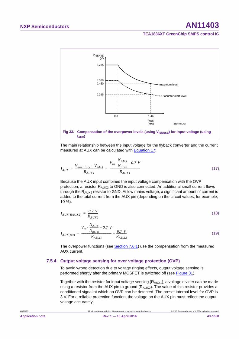
The main relationship between the input voltage for the flyback converter and the current measured at AUX can be calculated with Equation 17:
(17)
Because the AUX input combines the input voltage compensation with the OVP protection, a resistor RAUX2 to GND is also connected. An additional small current flows through the RAUX2 resistor to GND. At low mains voltage, a significant amount of current is added to the total current from the AUX pin (depending on the circuit values; for example, 10 %).
(18)
(19)
The overpower functions (see Section 7.6.1) use the compensation from the measured AUX current.
7.5.4 Output voltage sensing for over voltage protection (OVP)
To avoid wrong detection due to voltage ringing effects, output voltage sensing is performed shortly after the primary MOSFET is switched off (see Figure 31).
Together with the resistor for input voltage sensing (RAUX1), a voltage divider can be made using a resistor from the AUX pin to ground (RAUX2). The value of this resistor provides a conditioned signal at which an OVP can be detected. The preset internal level for OVP is 3 V. For a reliable protection function, the voltage on the AUX pin must reflect the output voltage accurately.
Fig 33. Compensation of the overpower levels (using VISENSE) for input voltage (using IAUX)
IAUX
Vauxiliary VAUX–
RAUX1------------------------------------------
Vin
NAUX
Nprim------------- 0.7 V–
RAUX1---------------------------------------------= =
IAUX RAUX2 0.7 VRAUX2---------------=
IAUX tot
Vin
NAUX
Nprim------------- 0.7 V–
RAUX1--------------------------------------------- 0.7 V
RAUX2---------------+=
AN11403 All information provided in this document is subject to legal disclaimers. © NXP Semiconductors N.V. 2014. All rights reserved.
Application note Rev. 1 — 18 April 2014 43 of 68

NXP Semiconductors AN11403TEA1836XT GreenChip SMPS control IC
The basic relationship (neglecting the output voltage drop via the output rectifier and output cable) between the auxiliary voltage and the output voltage is the transformer turns ratio:
(20)
The value of RAUX1 must be determined for the overpower function. The value for RAUX2 can be chosen to provide the correct protection level for the OVP.
(21)
(22)
Example:
• NAUXILIARY = NO
• RAUX1 = 47 k
• VO(ovp) = 25 V
• VAUX(ovp) = 3 V
7.6 Primary current sensing
The voltage across series resistor RSENSE measures the primary current through the MOSFET switch. The ISENSE pin on the TEA1836XT senses this voltage. In general, the peak level measured provides information about the power level.
The information about the input voltage (sensed by the AUX pin) and the current (sensed by the ISENSE pin) determine the power level.
The converter power levels are set using the Rsense resistor value. During start-up and operation, the voltage on the ISENSE pin is used to decide when to switch off the MOSFET or detect the various states of conversion.
Soft start
During soft start, the ISENSE pin constantly measures the voltage level on the pin. It limits the peak current by switching off the MOSFET when the voltage reaches Vopp(ISENSE) (= 500 mV) until the CTRL voltage drops to 5 V and start-up ends.
Frequency reduction mode
In this mode, the peak current is kept constant, regulating to a constant peak voltage of 207 mV on the ISENSE pin.
VAUXILIARY
VO----------------------------
NAUXILIARY
NO-----------------------------=
VAUXILIARY
NAUXILIARY
NO----------------------------- VO=
VAUX
RAUX2
RAUX1 RAUX2+-------------------------------------- VAUXILIARY
RAUX2
RAUX1 RAUX2+--------------------------------------
NAUXILIARY
NO----------------------------- VO= =
RAUX2
VAUX RAUX1NAUXILIARY
NO----------------------------- VO VAUX–-------------------------------------------------------------- 3 V 47 k
1 25 V 3 V–---------------------------------------- 6.4 k= = =
AN11403 All information provided in this document is subject to legal disclaimers. © NXP Semiconductors N.V. 2014. All rights reserved.
Application note Rev. 1 — 18 April 2014 44 of 68
NXP Semiconductors AN11403TEA1836XT GreenChip SMPS control IC
Overpower protection counter
When the voltage on the ISENSE pin exceeds the overpower protection level (between 295 mV and 500 mV depending on the mains voltage; see Figure 33), the overpower counter is started. When the counter has finished, a safe restart is performed after 800 ms. The counter delay time is 40 ms during start-up and 200 ms during operation.
The overpower counter is reset when, during one cycle, VISENSE is smaller than the protection level.
When the reference voltage on the ISENSE pin is close to the protection level, the generated continuous average output power can be higher than the expected power. Due to some variation of the ISENSE voltage over time, the counter can sometimes be reset.
Overpower limiting
A maximum allowed voltage on the ISENSE pin (between 450 mV and 765 mV depending on the mains voltage; see Figure 33) limits the output power. When a higher current is drawn from the converter output, the output voltage drops.
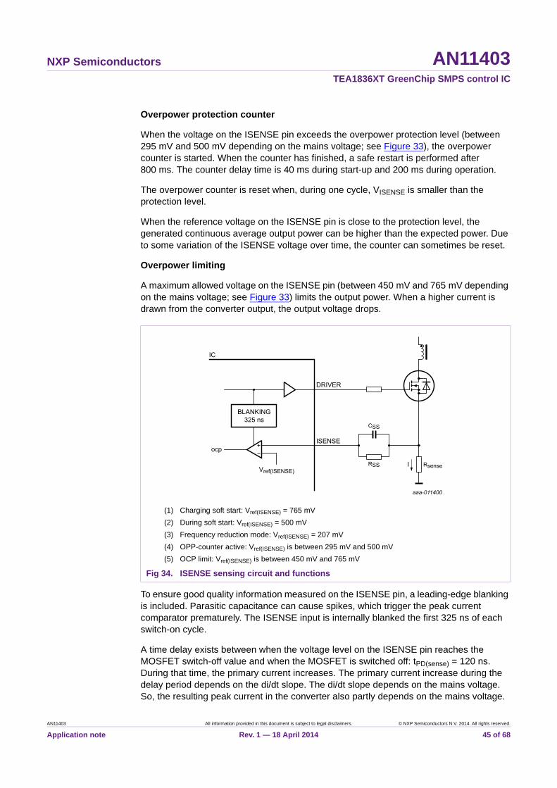
To ensure good quality information measured on the ISENSE pin, a leading-edge blanking is included. Parasitic capacitance can cause spikes, which trigger the peak current comparator prematurely. The ISENSE input is internally blanked the first 325 ns of each switch-on cycle.
A time delay exists between when the voltage level on the ISENSE pin reaches the MOSFET switch-off value and when the MOSFET is switched off: tPD(sense) = 120 ns. During that time, the primary current increases. The primary current increase during the delay period depends on the di/dt slope. The di/dt slope depends on the mains voltage. So, the resulting peak current in the converter also partly depends on the mains voltage.
(1) Charging soft start: Vref(ISENSE) = 765 mV
(2) During soft start: Vref(ISENSE) = 500 mV
(3) Frequency reduction mode: Vref(ISENSE) = 207 mV
(4) OPP-counter active: Vref(ISENSE) is between 295 mV and 500 mV
(5) OCP limit: Vref(ISENSE) is between 450 mV and 765 mV
Fig 34. ISENSE sensing circuit and functions
AN11403 All information provided in this document is subject to legal disclaimers. © NXP Semiconductors N.V. 2014. All rights reserved.
Application note Rev. 1 — 18 April 2014 45 of 68

NXP Semiconductors AN11403TEA1836XT GreenChip SMPS control IC
Under extreme conditions, the di/dt, depending on the transformer and converter design, can also rapidly increase because the transformer starts to saturate. These saturation conditions must be avoided because the converter operation is unpredictable.
7.6.1 OverPower Protection (OPP)
To realize a maximum output power which is constant over the complete mains voltage range, the overpower function uses the information on the ISENSE and AUX pins.
The overpower compensation circuit measures the input voltage via the AUX pin. The limiting voltage level for the ISENSE pin is determined from this measurement (see Figure 33).
If the measured voltage at the ISENSE pin exceeds the highest reference voltage (Vopc(ISENSE): a value between 450 mV and 765 mV), the DRIVER output is pulled low.
If the measured voltage on the ISENSE pins exceeds the lower reference voltage (Vopp(ISENSE): a value between 295 mV and 500 mV), the overpower counter starts.
By using two reference levels, the system allows 1.5 times more power (Vopc(ISENSE)) than the OPP power level on a cycle-by-cycle basis. When the overpower (Vopp(ISENSE)) level is exceeded, the overpower counter of 200 ms is triggered.
7.6.1.1 Overpower during start-up
During system start-up, the maximum overpower is limited to 100 %. The maximum time-out period is reduced to 40 ms. Once the output voltage is within its regulation level (VCTRL < 5 V), the maximum overpower is switched to 150 %. The maximum time-out period is increased to 200 ms.
Lowering the maximum output power and shortening the overpower timer during start-up ensures that the input power of the system is limited to < 5 W at a shorted output.
Fig 35. Leading-edge blanking and a higher peak current due to delay
AN11403 All information provided in this document is subject to legal disclaimers. © NXP Semiconductors N.V. 2014. All rights reserved.
Application note Rev. 1 — 18 April 2014 46 of 68

NXP Semiconductors AN11403TEA1836XT GreenChip SMPS control IC
7.6.1.2 Overpower and UVLO on the VCC pin
During a limited output power condition, the output voltage drops if the load requires more than 150 %. As a result, the voltage on the VCC pin drops as well and UVLO can be triggered. To obtain the same behavior in an overpower situation (whether UVLO is triggered or not), the system enters the protection mode (latch or safe restart) when overpower + UVLO is detected. The system entering the protection mode in this situation does not depend on the value of the OPP counter.
7.6.1.3 ISENSE reference levels modulated by input voltage
During high output power conditions, the voltage ripple on the input voltage of the flyback converter has an impact the compensation function of the AUX and ISENSE pins. Because the rectified mains voltage generates the input voltage, the bulk capacitor shows a ripple voltage when the output power is high. The result is that the average overpower levels are slightly lower at the lowest mains voltage or when a smaller value of the bulk capacitor is used.
7.7 Protections
If a protection is triggered, the controller stops switching. Depending on the protection triggered and the IC version, the protection causes a restart or latches the converter to an off state.
To avoid false triggering, some protections have a built-in delay.
When the system stops switching, the VCC pin is not supplied via the auxiliary winding anymore. In most cases, the internal current source on the HV pin continues mantains the VCC supply.
Releasing the latched protections can be achieved by disconnecting the mains voltage for a short time (see Section 7.7.3.3).
Table 4. Overview protections
Protection Delay Action VCC regulated
AUX open no wait until the AUX pin is connected
no
brownout 30 ms wait until Vmains > Vbrownin
yes
maximum on-time no safe restart 800 ms yes
OTP internal no latch yes
OTP via the PROTECT pin
2 ms to 4 ms latch yes
OVP via the AUX pin 4 driver pulses[1] latch yes
overpower compensation
no via the AUX pin; cycle-by-cycle
-
overpower time-out 40 ms or 200 ms safe restart 800 ms[2] yes
overpower + UVLO no safe restart 800 ms[2] yes
AN11403 All information provided in this document is subject to legal disclaimers. © NXP Semiconductors N.V. 2014. All rights reserved.
Application note Rev. 1 — 18 April 2014 47 of 68
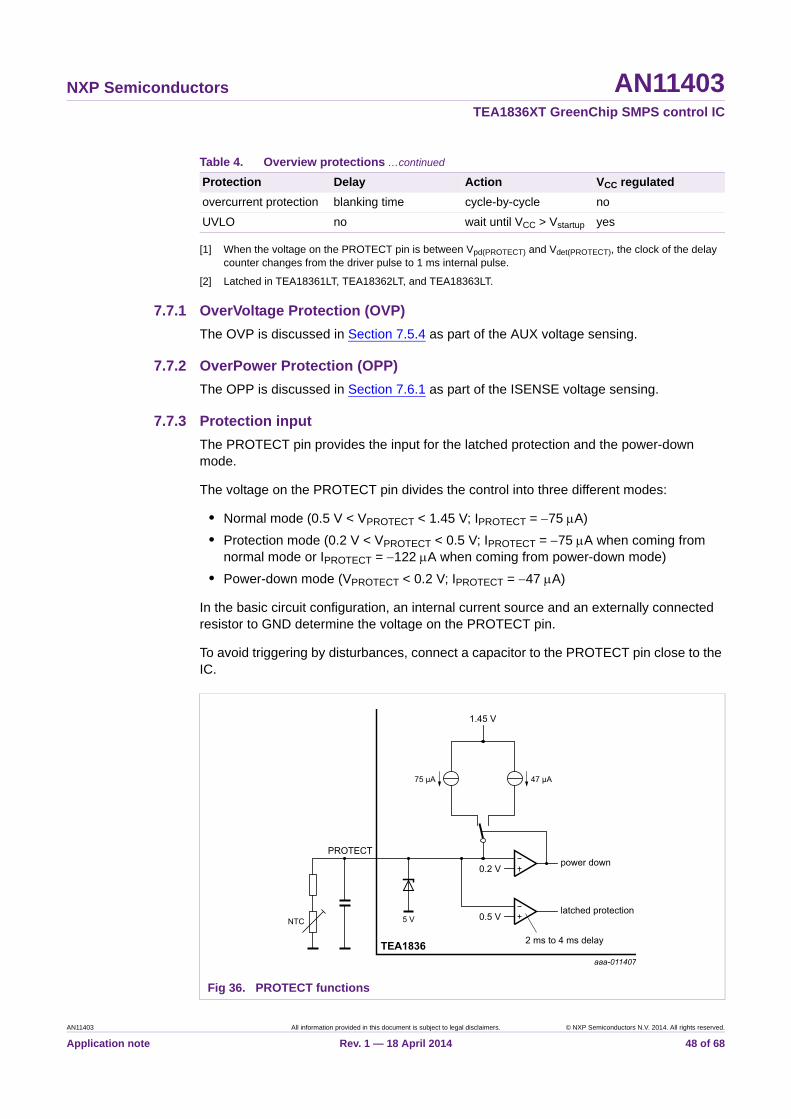
NXP Semiconductors AN11403TEA1836XT GreenChip SMPS control IC
[1] When the voltage on the PROTECT pin is between Vpd(PROTECT) and Vdet(PROTECT), the clock of the delay counter changes from the driver pulse to 1 ms internal pulse.
[2] Latched in TEA18361LT, TEA18362LT, and TEA18363LT.
7.7.1 OverVoltage Protection (OVP)
The OVP is discussed in Section 7.5.4 as part of the AUX voltage sensing.
7.7.2 OverPower Protection (OPP)
The OPP is discussed in Section 7.6.1 as part of the ISENSE voltage sensing.
7.7.3 Protection input
The PROTECT pin provides the input for the latched protection and the power-down mode.
The voltage on the PROTECT pin divides the control into three different modes:
• Normal mode (0.5 V < VPROTECT < 1.45 V; IPROTECT = 75 A)
• Protection mode (0.2 V < VPROTECT < 0.5 V; IPROTECT = 75 A when coming from normal mode or IPROTECT = 122 A when coming from power-down mode)
• Power-down mode (VPROTECT < 0.2 V; IPROTECT = 47 A)
In the basic circuit configuration, an internal current source and an externally connected resistor to GND determine the voltage on the PROTECT pin.
To avoid triggering by disturbances, connect a capacitor to the PROTECT pin close to the IC.
overcurrent protection blanking time cycle-by-cycle no
UVLO no wait until VCC > Vstartup yes
Table 4. Overview protections …continued
Protection Delay Action VCC regulated
Fig 36. PROTECT functions
AN11403 All information provided in this document is subject to legal disclaimers. © NXP Semiconductors N.V. 2014. All rights reserved.
Application note Rev. 1 — 18 April 2014 48 of 68
NXP Semiconductors AN11403TEA1836XT GreenChip SMPS control IC
7.7.3.1 Normal mode (0.5 V < VPROTECT < 1.45 V)
An internal clamp function limits the voltage on the PROTECT pin to 1.45 V. At start-up, the current sources are active before operation starts to set a normal mode starting condition. Normally, the voltage on the PROTECT pin is at the clamp level. It depends on the value of the connected resistor. The internal current source provides a value between 70 A and 80 A. When the resistor value is lower than 18 k, the voltage is lower than 1.45 V.
7.7.3.2 Latched protection (0.2 V < VPROTECT < 0.5 V)
A resistor is connected to GND at the PROTECT pin. An internal current source of 70 A determines the voltage on the PROTECT pin. This construction is chosen to provide an easy implementation of an external temperature sensing latched protection. Part of the external resistance can be an NTC resistor that is mechanically connected to a critical position in the application for monitoring the temperature. It stops operation if the temperature is too high. If the temperature increases, the resistance value of the NTC drops. When the protection level temperature is reached, the voltage on the PROTECT pin drops to below the trigger level (0.5 V).
After an internal delay of 2 ms to 4 ms, a latched protection is triggered. The delay avoids unwanted triggering.
Although the PROTECT pin configuration is very suitable for implementing an external overtemperature protection, it can also be used as a general purpose latched protection pin. Because of the internal delay and the combined power-down mode function (PROTECT < 0.2 V), care must be taken when connecting a protection function. A latched protection must be triggered by pulling down the voltage on PROTECT but not to below 0.2 V to prevent that the system enters the power-down mode.
Adding a capacitor between the PROTECT and GND pins helps to avoid a fast pull-down of the voltage and provides some extra noise filtering.
When the latched protection is triggered, the converter is stopped without restart sequence, so the VCC pin supply via auxiliary winding also stops. To maintain the latched protection state, the HV current supplies the VCC pin to 14.9 V.
7.7.3.3 Fast latch reset
To reset a latched protection, the voltage on the VCC pin must be < 8.65 V. During the latched protection state, the HV current supplies the VCC pin to 14.9 V.
Removing the mains voltage for a short time is the only way to restart the system. Only then the supply for the HV source stops and the VCC voltage drops to below 8.65 V because of the IC power consumption (220 A during the latched protection state). The time required to stop the supply depends on the value of the capacitor on the VCC (see Section 7.8).
The internal VCC discharge function helps to reduce the time required for resetting a latched protection by actively discharging VCC to 14.9 V with a 1.25 mA current. It avoids extra waiting time, especially when a large value VCC capacitor or a relatively high supply voltage is used. The same function is also used during a safe restart procedure.
AN11403 All information provided in this document is subject to legal disclaimers. © NXP Semiconductors N.V. 2014. All rights reserved.
Application note Rev. 1 — 18 April 2014 49 of 68

NXP Semiconductors AN11403TEA1836XT GreenChip SMPS control IC
7.7.3.4 Power-down mode (VPROTECT < 0.2 V)
The power-down mode is discussed in Section 7.9.
7.7.4 Safe restart sequence
If a protection is triggered and the system enters the safe restart mode, the system stops switching and restarts after an internally fixed period of 800 ms. While the converter is not switching, the HV current source supplies the VCC pin to 14.9 V. At restart, the system continues as in the normal start-up sequence (see Figure 21).
7.7.5 OverTemperature Protection (OTP)
An external temperature sensor can be connected to the PROTECT pin to provide overtemperature protection. Normally, an NTC resistor with a large value is used for good accuracy.
The IC incorporates an internal temperature sensor. This function triggers a latched protection when the internal temperature exceeds 140 C.
7.7.6 Maximum on-time
To prevent extreme power under fault conditions, the controller limits the driver on-time for the external MOSFET to 55 s. When the on-time is longer than 55 s, the IC stops switching and enters a safe restart cycle. Normally, the on-time is never reached unless there is a fault condition.
In applications that, for example, use a high primary inductance, while still requiring to generate high (peak) output power at a low input voltage, it is important to check the system for this limit during normal operation.
Fig 37. Fast latch reset
AN11403 All information provided in this document is subject to legal disclaimers. © NXP Semiconductors N.V. 2014. All rights reserved.
Application note Rev. 1 — 18 April 2014 50 of 68

NXP Semiconductors AN11403TEA1836XT GreenChip SMPS control IC
7.8 Active X-capacitor discharge
The HV pin provides the active X-capacitor discharge function. The HV pin also provides the high-voltage current source and mains sensing.
To suppress electromagnetic interference in most applications, a filter is required on the mains input. In addition to an inductance, EMI filters typically include one or more X-capacitors connected between the mains input terminals.
The voltage between the device mains terminals is reduced to a safe value within a certain time period after the device is disconnected from the mains. In some regulatory regimes, this reduction is mandatory. If the voltage is not reduced, there is a risk of electrical shock by inadvertently contacting the terminals of the plug.
In most applications, resistors between the mains connections provide this function. To limit circuit current consumption, the TEA1836XT activates this path only when required to provide the three functions on the HV pin.
When the mains voltage sensing does not detect a positive dV/dt (increasing values) for 28 ms, it assumes that the mains voltage is disconnected. The X-capacitor discharge function is started. During the X-capacitor discharge, the HV pin is switched to GND. The external X-capacitor is discharged using the externally connected resistor.
The resistor value determines the time to discharge the X-capacitor.
(23)
Example:
• X-capacitor value = 330 nF
• Series resistance is 50 k + 180 k = 230 k
• Highest expected voltage = 380 V
• Voltage on the HV pin (approximately 2.6 V) is neglected when discharging
Expected voltage after 28 ms detection delay and 0.2 s discharge:
To ensure the best protection against mains surges, the circuit to the HV pin can be connected between the CM choke and rectifier bridge. The CM choke provides filtering for surges. The X-capacitor can be discharged through the CM choke. There is also a voltage clamp for protection in the IC.
7.9 Power-down mode (VPROTECT < 0.2 V)
To activate the power-down mode, the voltage on the PROTECT pin can be pulled to GND level using an external switch. The optocoupler current becomes zero and the controller changes the regulation path for obtaining a low-power consumption condition. Not regulating the converter output voltage but only the voltage on the VCC pin gives a low-power consumption state.
Vxcap Vmains start e
tRC--------–
=
Vxcap 380 V e
0.2230 k 330 nF--------------------------------------------–
27.3 V= =
AN11403 All information provided in this document is subject to legal disclaimers. © NXP Semiconductors N.V. 2014. All rights reserved.
Application note Rev. 1 — 18 April 2014 51 of 68

NXP Semiconductors AN11403TEA1836XT GreenChip SMPS control IC
A short series of switching pulses keeps the voltage on the VCC pin high. The auxiliary winding, using the restart voltage regulation from the burst mode, supplies the VCC pin.
The power-down mode internally lowers the voltage on the CTRL pin to 0 V by switching off the internal source. The IC runs in burst mode (no-load condition), which maintains the voltage on the VCC pin. Generating a few switching cycles when the VCC reaches the restart level (11 V) maintains this voltage.
During switching, the transformer energy is distributed between the output and the auxiliary winding. At low output or no output load, the converter output voltage remains high. At higher loads, the voltage decreases, possibly even to zero. In this VCC regulation condition, the power converted to the output is low.
To limit the output voltage in a low output or no-load situation, the secondary circuit provides a voltage clamp function. Sensing the output voltage, the error amplifier increases the current through the optocoupler when the output voltage is near the regulation levels.
To increase the voltage on the PROTECT pin to normal mode quickly, the internal current source is extra high (122 A) when releasing the PROTECT pin to leave the power-down mode.
AN11403 All information provided in this document is subject to legal disclaimers. © NXP Semiconductors N.V. 2014. All rights reserved.
Application note Rev. 1 — 18 April 2014 52 of 68
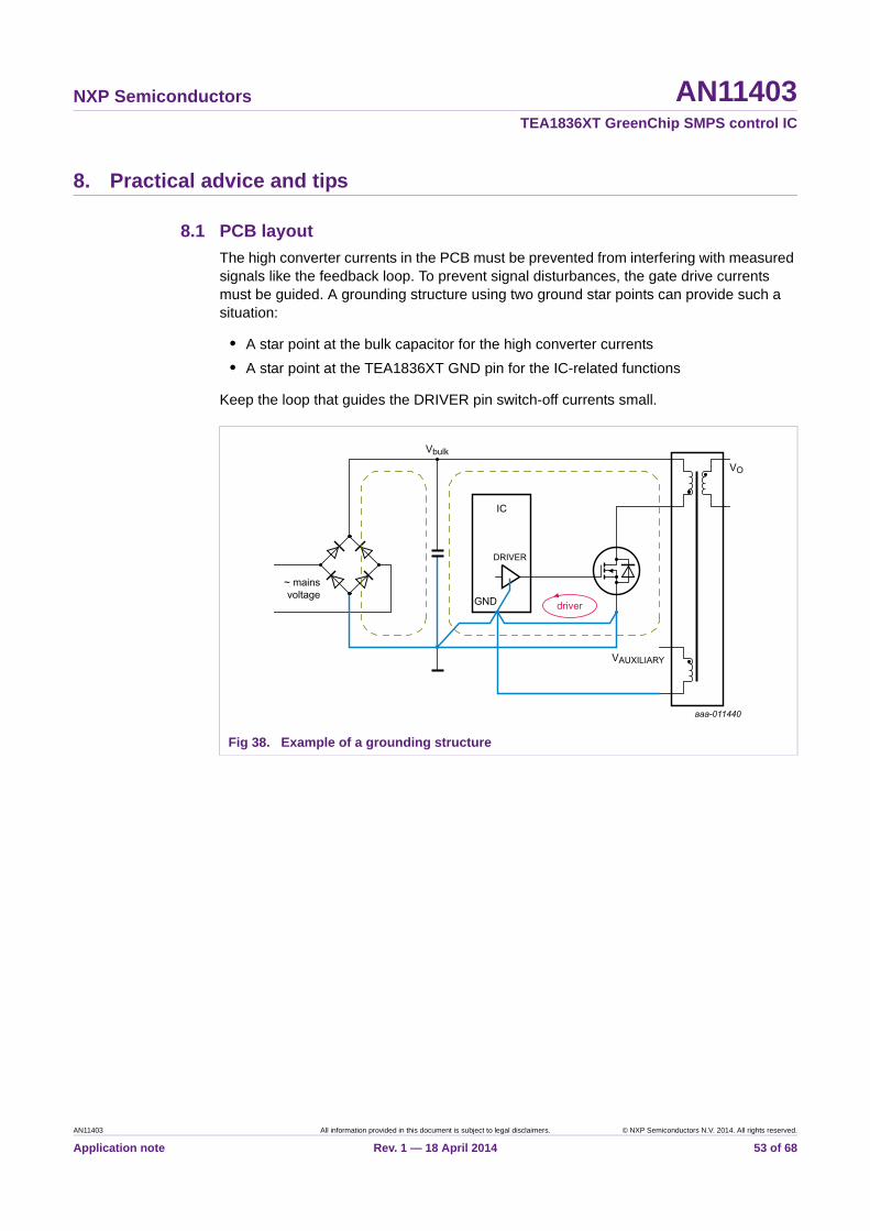
NXP Semiconductors AN11403TEA1836XT GreenChip SMPS control IC
8. Practical advice and tips
8.1 PCB layout
The high converter currents in the PCB must be prevented from interfering with measured signals like the feedback loop. To prevent signal disturbances, the gate drive currents must be guided. A grounding structure using two ground star points can provide such a situation:
• A star point at the bulk capacitor for the high converter currents
• A star point at the TEA1836XT GND pin for the IC-related functions
Keep the loop that guides the DRIVER pin switch-off currents small.
Fig 38. Example of a grounding structure
AN11403 All information provided in this document is subject to legal disclaimers. © NXP Semiconductors N.V. 2014. All rights reserved.
Application note Rev. 1 — 18 April 2014 53 of 68

NXP Semiconductors AN11403TEA1836XT GreenChip SMPS control IC
8.2 OPP, OVP and valley detection via the resistor divider on the AUX pin
The resistor divider RAUX1/RAUX2 for the AUX pin is shared for OVP detection and OPP compensation. RAUX1 is used for OPP compensation (current measurement). The complete resistor divider is used to set the OVP trip voltage (voltage measurement).
The AUX pin also provides the valley detection function. For accurate valley detection, the pin must be able to sense frequencies up to 500 kHz.
Distortion of the AUX signal can lead to a delay in valley detection. The effect on efficiency is very small but must be avoided, if possible. There are three ways to reduce the distortion:
• PCB layout ground structure (see Section 8.1)
• Not adding capacitance on the AUX pin
• Do not use high resistor values for RAUX1 + RAUX2
Fig 39. AUX sensing circuit and functions
AN11403 All information provided in this document is subject to legal disclaimers. © NXP Semiconductors N.V. 2014. All rights reserved.
Application note Rev. 1 — 18 April 2014 54 of 68
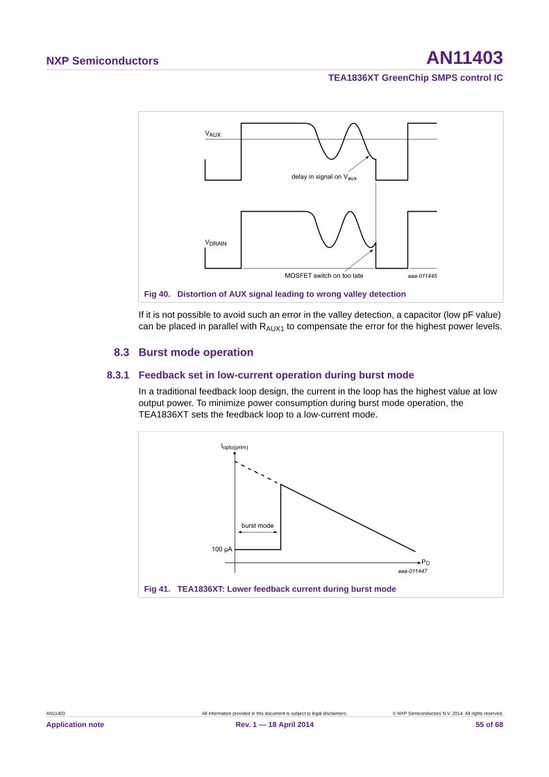
NXP Semiconductors AN11403TEA1836XT GreenChip SMPS control IC
If it is not possible to avoid such an error in the valley detection, a capacitor (low pF value) can be placed in parallel with RAUX1 to compensate the error for the highest power levels.
8.3 Burst mode operation
8.3.1 Feedback set in low-current operation during burst mode
In a traditional feedback loop design, the current in the loop has the highest value at low output power. To minimize power consumption during burst mode operation, the TEA1836XT sets the feedback loop to a low-current mode.
Fig 40. Distortion of AUX signal leading to wrong valley detection
Fig 41. TEA1836XT: Lower feedback current during burst mode
AN11403 All information provided in this document is subject to legal disclaimers. © NXP Semiconductors N.V. 2014. All rights reserved.
Application note Rev. 1 — 18 April 2014 55 of 68
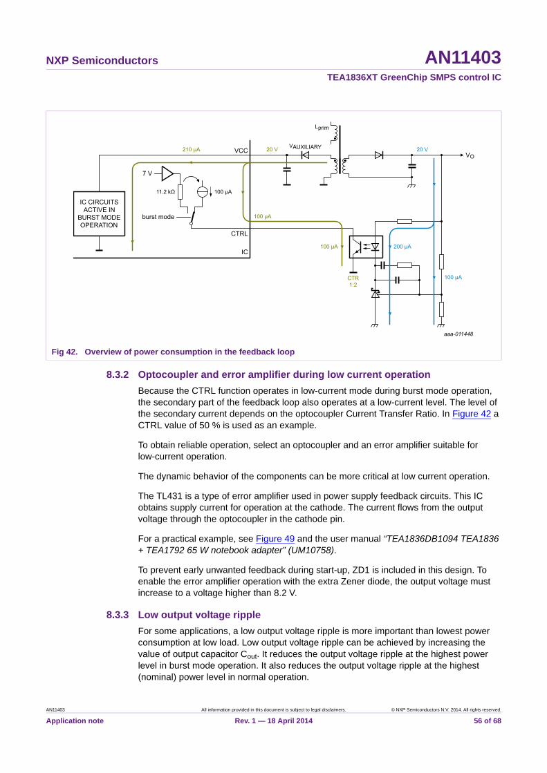
NXP Semiconductors AN11403TEA1836XT GreenChip SMPS control IC
8.3.2 Optocoupler and error amplifier during low current operation
Because the CTRL function operates in low-current mode during burst mode operation, the secondary part of the feedback loop also operates at a low-current level. The level of the secondary current depends on the optocoupler Current Transfer Ratio. In Figure 42 a CTRL value of 50 % is used as an example.
To obtain reliable operation, select an optocoupler and an error amplifier suitable for low-current operation.
The dynamic behavior of the components can be more critical at low current operation.
The TL431 is a type of error amplifier used in power supply feedback circuits. This IC obtains supply current for operation at the cathode. The current flows from the output voltage through the optocoupler in the cathode pin.
For a practical example, see Figure 49 and the user manual “TEA1836DB1094 TEA1836 + TEA1792 65 W notebook adapter” (UM10758).
To prevent early unwanted feedback during start-up, ZD1 is included in this design. To enable the error amplifier operation with the extra Zener diode, the output voltage must increase to a voltage higher than 8.2 V.
8.3.3 Low output voltage ripple
For some applications, a low output voltage ripple is more important than lowest power consumption at low load. Low output voltage ripple can be achieved by increasing the value of output capacitor Cout. It reduces the output voltage ripple at the highest power level in burst mode operation. It also reduces the output voltage ripple at the highest (nominal) power level in normal operation.
Fig 42. Overview of power consumption in the feedback loop
AN11403 All information provided in this document is subject to legal disclaimers. © NXP Semiconductors N.V. 2014. All rights reserved.
Application note Rev. 1 — 18 April 2014 56 of 68

NXP Semiconductors AN11403TEA1836XT GreenChip SMPS control IC
8.4 Transformer design
8.4.1 A combination of several aspects
• Efficiency requirements
• Transformer (core) size
• Peak power and core saturation
• EMI requirements
Figure 43 shows an overview of the main direct and indirect relationships between the design considerations above. Compromises must be made, while trying to achieve best performance. The following sections show the issues and provide a general guidance in making choices.
8.4.1.1 Relationship between the saturation current and the peak output power
(24)
(25)
(26)
Where:
•
•
•
• N is the transformer turns ratio
• Vin(min) (DC) is minimum voltage on the bulk capacitor
• IO is the output current
• VO is the output voltage
Fig 43. Overview relationships between the transformer choice and compromises
PO12--- Lp Ip
2fs =
Ip sat Np Bmax Ae
Lp-------------------------------------=
Ip max b– b
24 a c– +
2 a-------------------------------------------------------=
a N Vin min DC Lp=
b 2– IO Lp N VO Vf+ Vin min DC + =
c 2– IO tvalley N Vin min DC VO Vf+ =
AN11403 All information provided in this document is subject to legal disclaimers. © NXP Semiconductors N.V. 2014. All rights reserved.
Application note Rev. 1 — 18 April 2014 57 of 68

NXP Semiconductors AN11403TEA1836XT GreenChip SMPS control IC
• Vf is the voltage drop across the output rectifier
• tvalley is the time to reach a valley in the MOSFET drain voltage after demagnetization
• Lp is the value of the transformer primary inductance
In Section 6.2 a converter calculation flow is proposed. It includes the main functional parameters of the transformer.
8.4.2 Efficiency
To obtain a good efficiency performance, the primary inductance must be as high as possible. A high primary inductance prevents large peak currents that increase conduction losses in the converter. The primary inductance must, however, be low enough to support the required output power at the lowest input voltage.
For the TEA1836XT, the required output power must include the peak output power. Transformer saturation is a limiting parameter for this peak power according to the relationship given in Section 8.4.1.1. The thermal behavior is normally defined at nominal output power and not directly related to the peak power.
The size of the core used is the link between saturation and the primary inductance value. The inductance value affects the efficiency performance.
Because standard EMI requirements apply to all power supplies, the transformer must contain some internal shields to prevent extensive filtering at the input circuit or a high Y-capacitor value. They can be normal shields (copper tape) or winding shields.
To optimize efficiency for some turns, the wire diameter for primary and secondary windings can vary. When the required performance cannot be achieved, the number of turns can be modified to create a new optimization starting point. When changing the number of turns, the related parameters must be rechecked (see Figure 44).
AN11403 All information provided in this document is subject to legal disclaimers. © NXP Semiconductors N.V. 2014. All rights reserved.
Application note Rev. 1 — 18 April 2014 58 of 68
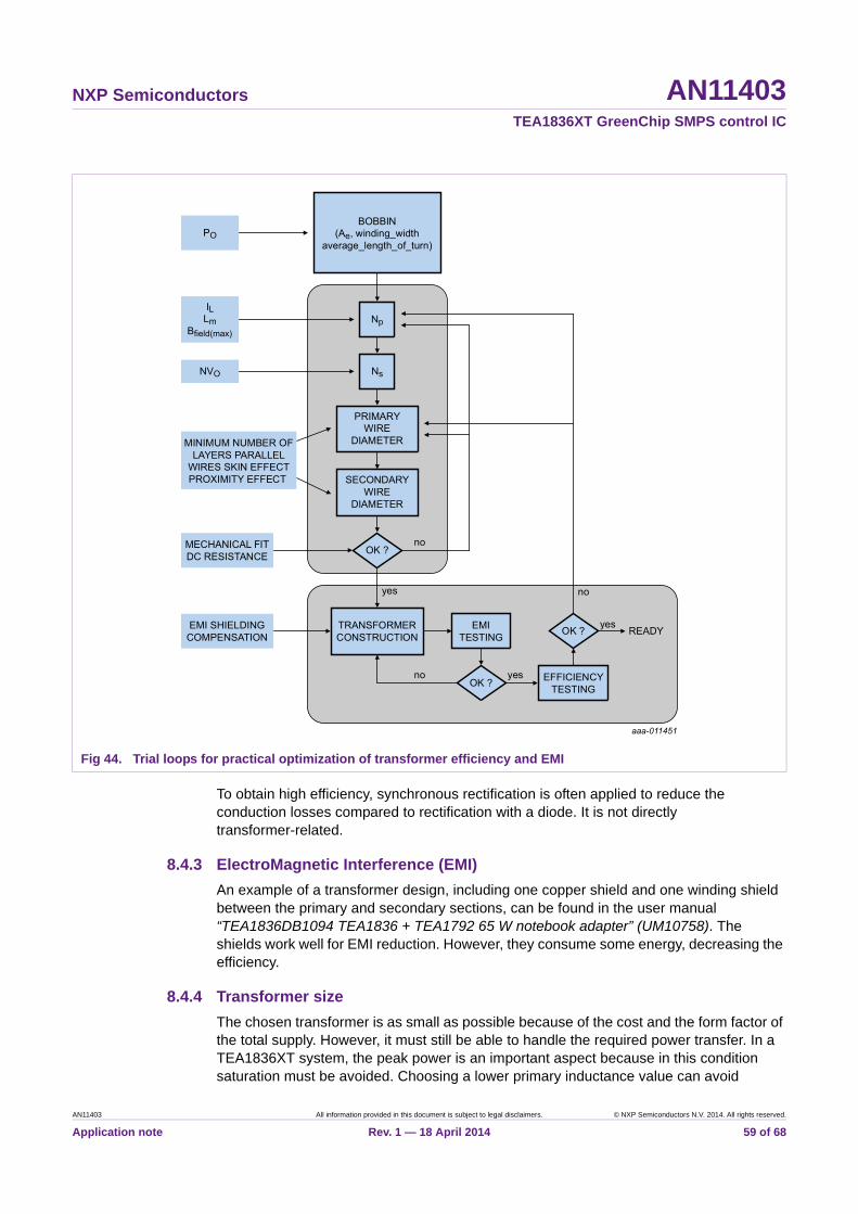
NXP Semiconductors AN11403TEA1836XT GreenChip SMPS control IC
To obtain high efficiency, synchronous rectification is often applied to reduce the conduction losses compared to rectification with a diode. It is not directly transformer-related.
8.4.3 ElectroMagnetic Interference (EMI)
An example of a transformer design, including one copper shield and one winding shield between the primary and secondary sections, can be found in the user manual “TEA1836DB1094 TEA1836 + TEA1792 65 W notebook adapter” (UM10758). The shields work well for EMI reduction. However, they consume some energy, decreasing the efficiency.
8.4.4 Transformer size
The chosen transformer is as small as possible because of the cost and the form factor of the total supply. However, it must still be able to handle the required power transfer. In a TEA1836XT system, the peak power is an important aspect because in this condition saturation must be avoided. Choosing a lower primary inductance value can avoid
Fig 44. Trial loops for practical optimization of transformer efficiency and EMI
AN11403 All information provided in this document is subject to legal disclaimers. © NXP Semiconductors N.V. 2014. All rights reserved.
Application note Rev. 1 — 18 April 2014 59 of 68

NXP Semiconductors AN11403TEA1836XT GreenChip SMPS control IC
saturation when using a small transformer. A disadvantage of such a choice is that the efficiency of the total system decreases. The efficiency decrease can conflict with the required efficiency level.
The TEA1836XT helps to limit the peak power to a short time (200 ms), limiting thermal consequences of enabling a high peak power.
8.4.5 Saturation at peak power
To avoid unpredictable behavior and spread between products, saturation of the transformer must be prevented. The most critical condition is at the highest peak output current when the input voltage is at the lowest level: low mains voltage rectified on the bulk capacitor showing the lowest voltage during a large voltage ripple condition.
The core size and the material determine the possibilities.
8.5 VCC supply using auxiliary winding
The voltage on an auxiliary winding during the secondary stroke is suitable for generating the supply to the VCC pin (see Figure 20). This level reflects the output voltage of the converter that is stabilized by regulation. The transformer design turns ratio Ns : NAUX can be used to obtain the correct voltage for the VCC pin. Rectification using a diode to the VCC capacitor provides a proper supply for the TEA1836XT.
Due to parasitic ringing, (see Section 5.2.1) the rectifier circuit can cause some deviation from the expected VCC level. Rectification of the highest ringing voltage from the source causes the deviation. Depending on the energy provided by the auxiliary winding during this ringing and the energy taken from VCC, a resulting higher voltage can be found. This deviation can vary by different load or input voltage conditions. The maximum VCC voltage must not exceed the limiting value of 30 V (or 35 V during a period < 100 ms).
To avoid rectification of one or more initial ringing peaks, a slower type of rectifier diode can be used.
8.6 DC input voltage and start-up (pin HV)
When a DC voltage at the mains input supplies the converter, the sensing circuit does not detect dV/dt. In this situation, the X-capacitor discharge function remains active continuously, resulting in an increase of input power consumption.
When the HV input current is above the brownout level, the IC starts up and operates normally.
Fig 45. Auxiliary winding voltage for supplying the VCC pin
AN11403 All information provided in this document is subject to legal disclaimers. © NXP Semiconductors N.V. 2014. All rights reserved.
Application note Rev. 1 — 18 April 2014 60 of 68

NXP Semiconductors AN11403TEA1836XT GreenChip SMPS control IC
8.7 TEA18362(L)T (8-pin version) without high-voltage spacer
When using the TEA18362(L)T (8-pin version of the TEA1836XT), it is important to consider the risk of application failures as a result of a short circuit between the HV and PROTECT pins during the product lifetime.
When the power supply is not in a completely closed encasing, dust or pollution can lead to a (semi-) short circuit condition between pins.
In general, it is valid for all adjacent pins. Without high-voltage spacer, it is also valid for pin HV and pin PROTECT.
8.7.1 Test mode on the PROTECT pin
If there is a high risk of a short circuit, check the behavior of the supply when the HV and PROTECT pins are shorted. If the behavior is not reliable, add three diodes between the PROTECT pin and GND as an extra measure for obtaining a safe situation.
In this way, the voltage on pin PROTECT cannot exceed 2.2 V when there is a short circuit between pin HV and pin PROTECT occurs. When the voltage exceeds 2.2 V, an IC test mode is triggered. In this test mode, internal logic disables the internal functions OTP, X-capacitor discharge, t(on)max, td(opp), and td(restart) during operation.
8.7.2 Practical short circuit testing between the PROTECT pin and the HV pin
When performing a short circuit test between the PROTECT pin (pin 7) and the HV pin (pin 8) of the TEA18362(L)T, the value of the capacitor on the PROTECT pin (CPROTECT) has an important influence. This capacitor is normally connected to suppress disturbances on the PROTECT pin. In the short circuit condition, it greatly reduces the accuracy of the mains sensing function on the HV pin.
Short 20 s measuring pulses (see Figure 47) perform the mains sensing.
Fig 46. TEA1836(L)T: 3 diodes added for obtaining a safe situation
AN11403 All information provided in this document is subject to legal disclaimers. © NXP Semiconductors N.V. 2014. All rights reserved.
Application note Rev. 1 — 18 April 2014 61 of 68

NXP Semiconductors AN11403TEA1836XT GreenChip SMPS control IC
When the HV pin is connected to the PROTECT pin, capacitor CPROTECT changes the typical mains voltage measurement into a more averaged voltage.
Normally, this change prevents that the system starts up when the short circuit is present before starting. It does not directly affect the operation when the short circuit is applied during normal operation conditions. The brownout level is affected.
Tests have shown that capacitor values for CPROTECT 22 nF lead to a stable and safe result during the test. Testing of an application is advised to observe the behavior.
Under short circuit conditions, the HV + PROTECT pin node shows a constant low voltage. Because of the constant low voltage, the RHV series resistors are a loaded continuously from the mains voltage, increasing the average power consumption of the resistors. Check the temperature of these resistors.
Figure 48 provides an overview of the functions related to the short circuit test between the HV pin and the PROTECT pin.
a. Mains voltage sensing: normal brownin and brownout
b. Mains voltage sensing: normal sensing by dV/dt detection and disconnecting the mains voltage
Fig 47. Normal mains sensing sequences
AN11403 All information provided in this document is subject to legal disclaimers. © NXP Semiconductors N.V. 2014. All rights reserved.
Application note Rev. 1 — 18 April 2014 62 of 68
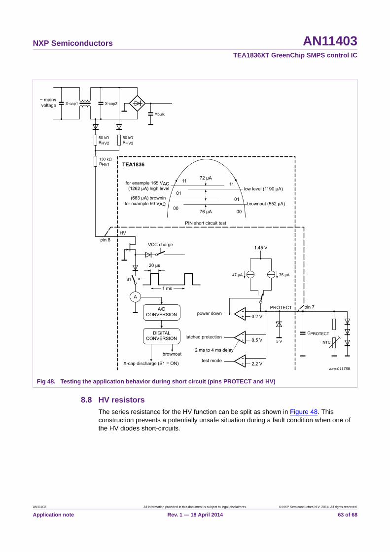
NXP Semiconductors AN11403TEA1836XT GreenChip SMPS control IC
8.8 HV resistors
The series resistance for the HV function can be split as shown in Figure 48. This construction prevents a potentially unsafe situation during a fault condition when one of the HV diodes short-circuits.
Fig 48. Testing the application behavior during short circuit (pins PROTECT and HV)
AN11403 All information provided in this document is subject to legal disclaimers. © NXP Semiconductors N.V. 2014. All rights reserved.
Application note Rev. 1 — 18 April 2014 63 of 68
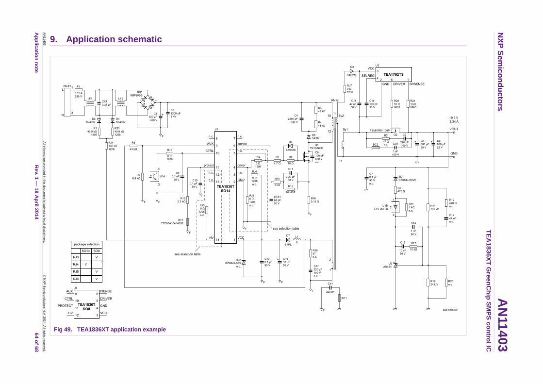
xxxxxxxxxxxxxxxxxxxxx xxxxxxxxxxxxxxxxxxxxxxxxxx xxxxxxx x x x xxxxxxxxxxxxxxxxxxxxxxxxxxxxxx xxxxxxxxxxxxxxxxxxx xx xx xxxxx xxxxxxxxxxxxxxxxxxxxxxxxxxx xxxxxxxxxxxxxxxxxxx xxxxxx xxxxxxxxxxxxxxxxxxxxxxxxxxxxxxxxxxx xxxxxxxxxxxx x x xxxxxxxxxxxxxxxxxxxxx xxxxxxxxxxxxxxxxxxxxxxxxxxxxxx xxxxx xxxxxxxxxxxxxxxxxxxxxxxxxxxxxxxxxxxxxxxxxxxxxxxxxx xxxxxxxx xxxxxxxxxxxxxxxxxxxxxxxxx xxxxxxxxxxxxxxxxxxxx xxx
AN
11403
Ap
plicatio
n n
ote
NX
P S
emico
nd
ucto
rsA
N11403
TE
A18
36X
T G
reen
Ch
ip S
MP
S co
ntro
l IC
9. Application schematic
All inform
ation provided
in this docum
ent is subject to leg
al disclaim
ers.©
NX
P S
em
iconductors N
.V. 2014. A
ll rights reserved.
Rev. 1
— 18 A
pril 2014
64 of 68
Fig 49. TEA1836XT application example

NXP Semiconductors AN11403TEA1836XT GreenChip SMPS control IC
10. Abbreviations
11. References
[1] UM10758 — TEA1836DB1094 TEA1836XT + TEA1792T 65 W notebook adapter
Table 5. Abbreviations
Acronym Description
BCM Boundary Conduction Mode
CCM Continuous Conduction Mode
CM Common-Mode
DCM Discontinuous Conduction Mode
EMI ElectroMagnetic Interference
LVS Low-Voltage Switch
MOSFET Metal-Oxide Semiconductor Field-Effect Transistor
OCP OverCurrent Protection
OLP Open-Loop Protection
OPP OverPower Protection
OTP OverTemperature Protection
OVP OverVoltage Protection
PCB Printed-Circuit Board
PFC Power Factor Correction
QR Quasi-Resonant
RMS Root Mean Square
SOI Silicon-On Insulator
SR Synchronous Rectification
ZVS Zero Voltage Switching
AN11403 All information provided in this document is subject to legal disclaimers. © NXP Semiconductors N.V. 2014. All rights reserved.
Application note Rev. 1 — 18 April 2014 65 of 68

NXP Semiconductors AN11403TEA1836XT GreenChip SMPS control IC
12. Legal information
12.1 Definitions
Draft — The document is a draft version only. The content is still under internal review and subject to formal approval, which may result in modifications or additions. NXP Semiconductors does not give any representations or warranties as to the accuracy or completeness of information included herein and shall have no liability for the consequences of use of such information.
12.2 Disclaimers
Limited warranty and liability — Information in this document is believed to be accurate and reliable. However, NXP Semiconductors does not give any representations or warranties, expressed or implied, as to the accuracy or completeness of such information and shall have no liability for the consequences of use of such information. NXP Semiconductors takes no responsibility for the content in this document if provided by an information source outside of NXP Semiconductors.
In no event shall NXP Semiconductors be liable for any indirect, incidental, punitive, special or consequential damages (including - without limitation - lost profits, lost savings, business interruption, costs related to the removal or replacement of any products or rework charges) whether or not such damages are based on tort (including negligence), warranty, breach of contract or any other legal theory.
Notwithstanding any damages that customer might incur for any reason whatsoever, NXP Semiconductors’ aggregate and cumulative liability towards customer for the products described herein shall be limited in accordance with the Terms and conditions of commercial sale of NXP Semiconductors.
Right to make changes — NXP Semiconductors reserves the right to make changes to information published in this document, including without limitation specifications and product descriptions, at any time and without notice. This document supersedes and replaces all information supplied prior to the publication hereof.
Suitability for use — NXP Semiconductors products are not designed, authorized or warranted to be suitable for use in life support, life-critical or safety-critical systems or equipment, nor in applications where failure or malfunction of an NXP Semiconductors product can reasonably be expected to result in personal injury, death or severe property or environmental damage. NXP Semiconductors and its suppliers accept no liability for inclusion and/or use of NXP Semiconductors products in such equipment or applications and therefore such inclusion and/or use is at the customer’s own risk.
Applications — Applications that are described herein for any of these products are for illustrative purposes only. NXP Semiconductors makes no representation or warranty that such applications will be suitable for the specified use without further testing or modification.
Customers are responsible for the design and operation of their applications and products using NXP Semiconductors products, and NXP Semiconductors accepts no liability for any assistance with applications or customer product
design. It is customer’s sole responsibility to determine whether the NXP Semiconductors product is suitable and fit for the customer’s applications and products planned, as well as for the planned application and use of customer’s third party customer(s). Customers should provide appropriate design and operating safeguards to minimize the risks associated with their applications and products.
NXP Semiconductors does not accept any liability related to any default, damage, costs or problem which is based on any weakness or default in the customer’s applications or products, or the application or use by customer’s third party customer(s). Customer is responsible for doing all necessary testing for the customer’s applications and products using NXP Semiconductors products in order to avoid a default of the applications and the products or of the application or use by customer’s third party customer(s). NXP does not accept any liability in this respect.
Export control — This document as well as the item(s) described herein may be subject to export control regulations. Export might require a prior authorization from competent authorities.
Evaluation products — This product is provided on an “as is” and “with all faults” basis for evaluation purposes only. NXP Semiconductors, its affiliates and their suppliers expressly disclaim all warranties, whether express, implied or statutory, including but not limited to the implied warranties of non-infringement, merchantability and fitness for a particular purpose. The entire risk as to the quality, or arising out of the use or performance, of this product remains with customer.
In no event shall NXP Semiconductors, its affiliates or their suppliers be liable to customer for any special, indirect, consequential, punitive or incidental damages (including without limitation damages for loss of business, business interruption, loss of use, loss of data or information, and the like) arising out the use of or inability to use the product, whether or not based on tort (including negligence), strict liability, breach of contract, breach of warranty or any other theory, even if advised of the possibility of such damages.
Notwithstanding any damages that customer might incur for any reason whatsoever (including without limitation, all damages referenced above and all direct or general damages), the entire liability of NXP Semiconductors, its affiliates and their suppliers and customer’s exclusive remedy for all of the foregoing shall be limited to actual damages incurred by customer based on reasonable reliance up to the greater of the amount actually paid by customer for the product or five dollars (US$5.00). The foregoing limitations, exclusions and disclaimers shall apply to the maximum extent permitted by applicable law, even if any remedy fails of its essential purpose.
Translations — A non-English (translated) version of a document is for reference only. The English version shall prevail in case of any discrepancy between the translated and English versions.
12.3 TrademarksNotice: All referenced brands, product names, service names and trademarks are the property of their respective owners.
GreenChip — is a trademark of NXP Semiconductors N.V.
AN11403 All information provided in this document is subject to legal disclaimers. © NXP Semiconductors N.V. 2014. All rights reserved.
Application note Rev. 1 — 18 April 2014 66 of 68

NXP Semiconductors AN11403TEA1836XT GreenChip SMPS control IC
13. Contents
1 Introduction . . . . . . . . . . . . . . . . . . . . . . . . . . . . 3
2 Features and applications. . . . . . . . . . . . . . . . . 32.1 General features. . . . . . . . . . . . . . . . . . . . . . . . 32.2 Green features . . . . . . . . . . . . . . . . . . . . . . . . . 32.3 Protection features . . . . . . . . . . . . . . . . . . . . . . 32.4 Applications . . . . . . . . . . . . . . . . . . . . . . . . . . . 4
3 Pinning . . . . . . . . . . . . . . . . . . . . . . . . . . . . . . . . 43.1 Pin descriptions . . . . . . . . . . . . . . . . . . . . . . . . 4
4 Application block diagram . . . . . . . . . . . . . . . . 9
5 Flyback converter operating modes . . . . . . . 105.1 TEA1836XT flyback operating modes . . . . . . 105.2 DCM flyback conversion. . . . . . . . . . . . . . . . . 115.2.1 Parasitic elements . . . . . . . . . . . . . . . . . . . . . 125.3 Quasi-Resonant (QR) mode. . . . . . . . . . . . . . 125.3.1 Three situations related to the input voltage
and output voltage . . . . . . . . . . . . . . . . . . . . . 135.3.2 Quasi-resonant mode in the TEA1836XT. . . . 135.4 Discontinuous Conduction Mode (DCM) . . . . 145.4.1 DCM in the TEA1836XT . . . . . . . . . . . . . . . . . 145.5 Burst mode . . . . . . . . . . . . . . . . . . . . . . . . . . . 145.5.1 Burst mode in TEA1836XT. . . . . . . . . . . . . . . 155.5.1.1 Low power consumption. . . . . . . . . . . . . . . . . 155.5.1.2 Audible noise . . . . . . . . . . . . . . . . . . . . . . . . . 155.5.1.3 Regulation by feedback (VCTRL) and internal
digital control. . . . . . . . . . . . . . . . . . . . . . . . . . 15
6 Introduction to flyback converter design . . . 166.1 Converter design including OverPower
Protection (OPP) . . . . . . . . . . . . . . . . . . . . . . 166.2 Transformer parameters design flow . . . . . . . 176.2.1 Bulk capacitor value . . . . . . . . . . . . . . . . . . . . 186.2.1.1 Demo board example . . . . . . . . . . . . . . . . . . . 196.2.2 Transformer saturation margin at maximum
peak power . . . . . . . . . . . . . . . . . . . . . . . . . . . 216.2.3 Relationship between transformer saturation
current and inductance . . . . . . . . . . . . . . . . . . 216.2.4 Transformer winding ratio (N, Ns, and Np) . . . 226.2.5 Relationship between maximum peak current
and inductance . . . . . . . . . . . . . . . . . . . . . . . . 236.2.6 Resistor Rsense . . . . . . . . . . . . . . . . . . . . . . . . 246.2.7 Relationship between switching frequency
and inductance . . . . . . . . . . . . . . . . . . . . . . . . 246.2.8 Relationship between inductance value
and efficiency . . . . . . . . . . . . . . . . . . . . . . . . . 26
7 TEA1836XT functional description. . . . . . . . . 277.1 Start-up (HV pin) . . . . . . . . . . . . . . . . . . . . . . . 277.1.1 Start-up with the HV current source . . . . . . . . 27
7.1.2 Start-up sequence . . . . . . . . . . . . . . . . . . . . . 287.1.3 Soft start. . . . . . . . . . . . . . . . . . . . . . . . . . . . . 297.2 Modes of operation . . . . . . . . . . . . . . . . . . . . 307.2.1 Feedback control (CTRL pin). . . . . . . . . . . . . 307.2.2 Normal mode operation . . . . . . . . . . . . . . . . . 317.2.3 Burst mode operation. . . . . . . . . . . . . . . . . . . 337.2.3.1 Primary peak current during a burst. . . . . . . . 347.2.3.2 The burst sequence and target number
of pulses. . . . . . . . . . . . . . . . . . . . . . . . . . . . . 357.2.3.3 Sensing for a load step requesting more
power (ICTRL < 90 mA) . . . . . . . . . . . . . . . . . . 357.2.3.4 Sensing for too much power in a burst
(ICTRL > 750 mA) . . . . . . . . . . . . . . . . . . . . . . 367.2.3.5 Feedback circuit behavior in burst mode
operation . . . . . . . . . . . . . . . . . . . . . . . . . . . . 367.3 MOSFET driver . . . . . . . . . . . . . . . . . . . . . . . 377.4 Mains voltage sensing (pin HV) . . . . . . . . . . . 377.4.1 Mains sense circuit . . . . . . . . . . . . . . . . . . . . 387.4.2 Brownin . . . . . . . . . . . . . . . . . . . . . . . . . . . . . 387.4.3 Brownout . . . . . . . . . . . . . . . . . . . . . . . . . . . . 397.4.3.1 Detecting disconnected mains and activating
X-capacitor discharge . . . . . . . . . . . . . . . . . . 407.4.4 Mains sensing in burst mode . . . . . . . . . . . . . 407.5 Auxiliary winding . . . . . . . . . . . . . . . . . . . . . . 407.5.1 Demagnetization detection . . . . . . . . . . . . . . 417.5.2 Valley detection . . . . . . . . . . . . . . . . . . . . . . . 417.5.3 Input voltage sensing for compensation . . . . 427.5.4 Output voltage sensing for over voltage
protection (OVP) . . . . . . . . . . . . . . . . . . . . . . 437.6 Primary current sensing . . . . . . . . . . . . . . . . . 447.6.1 OverPower Protection (OPP). . . . . . . . . . . . . 467.6.1.1 Overpower during start-up . . . . . . . . . . . . . . . 467.6.1.2 Overpower and UVLO on the VCC pin . . . . . 477.6.1.3 ISENSE reference levels modulated by
input voltage. . . . . . . . . . . . . . . . . . . . . . . . . . 477.7 Protections . . . . . . . . . . . . . . . . . . . . . . . . . . . 477.7.1 OverVoltage Protection (OVP) . . . . . . . . . . . . 487.7.2 OverPower Protection (OPP). . . . . . . . . . . . . 487.7.3 Protection input . . . . . . . . . . . . . . . . . . . . . . . 487.7.3.1 Normal mode (0.5 V < VPROTECT < 1.45 V) . . 497.7.3.2 Latched protection (0.2 V < VPROTECT < 0.5 V) 497.7.3.3 Fast latch reset . . . . . . . . . . . . . . . . . . . . . . . 497.7.3.4 Power-down mode (VPROTECT < 0.2 V) . . . . . 507.7.4 Safe restart sequence . . . . . . . . . . . . . . . . . . 507.7.5 OverTemperature Protection (OTP) . . . . . . . . 507.7.6 Maximum on-time . . . . . . . . . . . . . . . . . . . . . 507.8 Active X-capacitor discharge . . . . . . . . . . . . . 517.9 Power-down mode (VPROTECT < 0.2 V) . . . . . 51
AN11403 All information provided in this document is subject to legal disclaimers. © NXP Semiconductors N.V. 2014. All rights reserved.
Application note Rev. 1 — 18 April 2014 67 of 68
continued >>
NXP Semiconductors AN11403TEA1836XT GreenChip SMPS control IC
8 Practical advice and tips . . . . . . . . . . . . . . . . . 538.1 PCB layout . . . . . . . . . . . . . . . . . . . . . . . . . . . 538.2 OPP, OVP and valley detection via the resistor
divider on the AUX pin . . . . . . . . . . . . . . . . . . 548.3 Burst mode operation . . . . . . . . . . . . . . . . . . . 558.3.1 Feedback set in low-current operation during
burst mode . . . . . . . . . . . . . . . . . . . . . . . . . . . 558.3.2 Optocoupler and error amplifier during low
current operation . . . . . . . . . . . . . . . . . . . . . . 568.3.3 Low output voltage ripple . . . . . . . . . . . . . . . . 568.4 Transformer design. . . . . . . . . . . . . . . . . . . . . 578.4.1 A combination of several aspects . . . . . . . . . . 578.4.1.1 Relationship between the saturation current
and the peak output power . . . . . . . . . . . . . . . 578.4.2 Efficiency . . . . . . . . . . . . . . . . . . . . . . . . . . . . 588.4.3 ElectroMagnetic Interference (EMI) . . . . . . . . 598.4.4 Transformer size. . . . . . . . . . . . . . . . . . . . . . . 598.4.5 Saturation at peak power . . . . . . . . . . . . . . . . 608.5 VCC supply using auxiliary winding . . . . . . . . 608.6 DC input voltage and start-up (pin HV). . . . . . 608.7 TEA18362(L)T (8-pin version) without
high-voltage spacer . . . . . . . . . . . . . . . . . . . . 618.7.1 Test mode on the PROTECT pin . . . . . . . . . . 618.7.2 Practical short circuit testing between the
PROTECT pin and the HV pin . . . . . . . . . . . . 618.8 HV resistors . . . . . . . . . . . . . . . . . . . . . . . . . . 63
9 Application schematic. . . . . . . . . . . . . . . . . . . 64
10 Abbreviations. . . . . . . . . . . . . . . . . . . . . . . . . . 65
11 References . . . . . . . . . . . . . . . . . . . . . . . . . . . . 65
12 Legal information. . . . . . . . . . . . . . . . . . . . . . . 6612.1 Definitions. . . . . . . . . . . . . . . . . . . . . . . . . . . . 6612.2 Disclaimers . . . . . . . . . . . . . . . . . . . . . . . . . . . 6612.3 Trademarks. . . . . . . . . . . . . . . . . . . . . . . . . . . 66
13 Contents . . . . . . . . . . . . . . . . . . . . . . . . . . . . . . 67
© NXP Semiconductors N.V. 2014. All rights reserved.
For more information, please visit: http://www.nxp.comFor sales office addresses, please send an email to: [email protected]
Date of release: 18 April 2014
Document identifier: AN11403
Please be aware that important notices concerning this document and the product(s)described herein, have been included in section ‘Legal information’.