an1560: making accurate voltage noise and current noise ... · pdf filemaking accurate voltage...
TRANSCRIPT

Making Accurate Voltage Noise and Current Noise Measurementson Operational Amplifiers Down to 0.1Hz
APPLICATION NOTE
AN1560Rev.1.00
Jan 11, 2011
AbstractMaking accurate voltage and current noise measurements on op amps in the nV and fA range can be challenging. This problem is often addressed by two different approaches. Both approaches concentrate on reducing the noise of the amplifiers used to measure the Device Under Test (DUT). The first approach uses conventional cross-correlation techniques to remove un-correlated noise and a procedure to remove the correlated noise contributions made by the amplifiers used to measure the DUT [1]. The second approach, and the subject of this Application Note, consists of designing a test platform with an effective background noise at least 10dB lower than the DUT.
To obtain a test platform with this level of performance requires: the removal of environmental electrical disturbances, the use of batteries for low noise voltage sources, the use of a Post Amplifier (PA) to raise the DUT noise above the measurement system’s noise floor, control software to measure accurate noise data down to 0.1Hz and processing software to eliminate external noise and generate the DUT’s voltage (en) and current (in) noise plots.
This Application Note will discuss the procedures used to obtain a test platform that is capable of measuring nV and fA down to 0.1Hz. The test platform’s capability is illustrated by measuring the voltage and current noise of Intersil’s ISL28190 (Bipolar inputs, 1nV/√Hz) operational amplifier and Intersil’s ISL28148 (MOS inputs, 16fA/√Hz) operational amplifier.
IntroductionTo measure an accurate internal noise of an Op Amp, for a data sheet spec, two types of external noise sources (Environmental and Johnson) must be removed from the measurement. Environmental noise is any unwanted signals arriving as either voltage or current, at any of the amplifiers terminals or surrounding circuitry. It can appear as spikes, steps, sign waves or random noise. This noise can come from anywhere: nearby machinery, power lines, RF transmitters, lab power supplies or lab computers. The Environmental noise is minimized by isolating the DUT in a Faraday cage and powering the DUT with batteries.
The second external noise source is Johnson noise. Johnson noise is the noise generated by the external biasing and gain setting resistors of the DUT and test platform. Johnson noise is subtracted out from the total noise measurement through processing software so only the internal noise of the DUT is reported.
This Application Note will:
1. Discuss basic noise equations (external and internal) and then use these equations to extract the DUT noise from our test platform’s noise.
2. Discuss the use of a Post Amplifier (PA) to lower our HP35670A Dynamic Signal Analyzer’s (DSA) effective noise floor from 20nV/√Hz to 3nV/√Hz.
3. Illustrate the effectiveness of our Faraday cage to remove environmental noise.
4. Discuss AC coupling of DUT, PA and DSA.5. Determine the required gain of the DUT to enable
the test platform to measure voltage noise below 3nV/√Hz.
6. Discuss considerations for choosing the optimum series resistor RS to measure current noise.
7. Discuss the Test Platform Algorithm.8. Present conclusions.
Basic Equations For Calculating NoiseJohnson noise is the only resistive noise source considered in this controlled lab study. Other resistive noise sources such as contact noise, shot noise and parasitics associated with particular types of resistors could also contribute noise in an application.
A typical figure of merit for amplifier noise is noise density. Voltage-noise density is specified in nV/√Hz, while current-noise density is usually in units of pA/√Hz [2]. For simplicity, these measurements are referred to the amplifier inputs; thus removing the need to account for the amplifiers gain.
External Johnson NoiseAt temperatures above absolute zero, all resistances generate Johnson noise due to the thermal movement of charge carriers. This noise increases with resistance, temperature and bandwidth. The voltage and current noise are given by Equations 1 and 2, respectively [3, 4, 5].
External Johnson Voltage Noise
External Johnson Current Noise
Where:
k is Boltzmann’s constant (1.38 x 10⁻²³ J/K).
T is the temperature in Kelvin (273.15 + Ambient C).
R is the resistance (Ω)
B is the bandwidth in Hz.
Vn en 4kTBR= = (EQ. 1)
in4kTB
R---------------= (EQ. 2)
AN1560 Rev.1.00 Page 1 of 9Jan 11, 2011
Making Accurate Voltage Noise and Current Noise
Measurements on Operational Amplifiers Down to 0.1Hz
Note: Bandwidth is 1Hz for all measurements and not shown in all Equations presented in the Application Note.
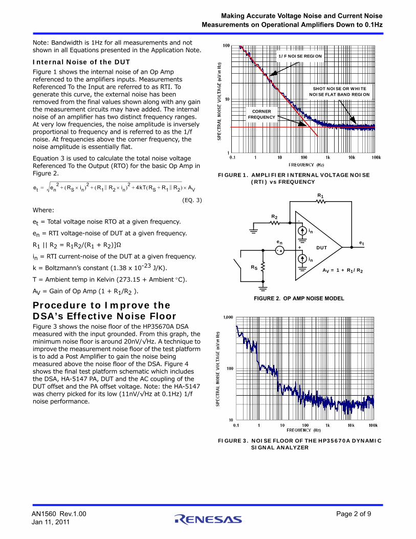
Internal Noise of the DUTFigure 1 shows the internal noise of an Op Amp referenced to the amplifiers inputs. Measurements Referenced To the Input are referred to as RTI. To generate this curve, the external noise has been removed from the final values shown along with any gain the measurement circuits may have added. The internal noise of an amplifier has two distinct frequency ranges. At very low frequencies, the noise amplitude is inversely proportional to frequency and is referred to as the 1/f noise. At frequencies above the corner frequency, the noise amplitude is essentially flat.
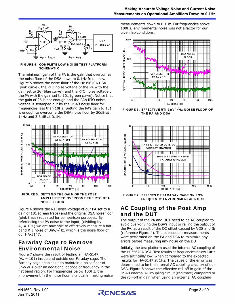
Equation 3 is used to calculate the total noise voltage Referenced To the Output (RTO) for the basic Op Amp in Figure 2.
Where:
et = Total voltage noise RTO at a given frequency.
en = RTI voltage-noise of DUT at a given frequency.
R1 || R2 = R1R2/(R1 + R2)]Ω
in = RTI current-noise of the DUT at a given frequency.
k = Boltzmann’s constant (1.38 x 10⁻²³ J/K).
T = Ambient temp in Kelvin (273.15 + Ambient C).
AV = Gain of Op Amp (1 + R1/R2 ).
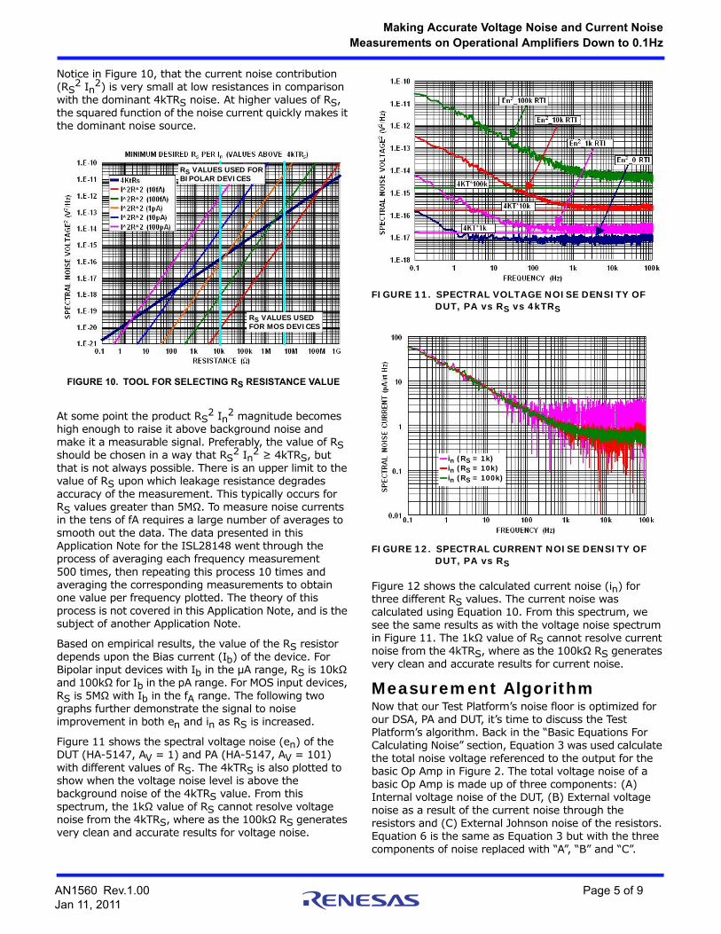
Procedure to Improve the DSA’s Effective Noise FloorFigure 3 shows the noise floor of the HP35670A DSA measured with the input grounded. From this graph, the minimum noise floor is around 20nV/√Hz. A technique to improve the measurement noise floor of the test platform is to add a Post Amplifier to gain the noise being measured above the noise floor of the DSA. Figure 4 shows the final test platform schematic which includes the DSA, HA-5147 PA, DUT and the AC coupling of the DUT offset and the PA offset voltage. Note: the HA-5147 was cherry picked for its low (11nV/√Hz at 0.1Hz) 1/f noise performance.
et en2
RS in 2 R1 R2 in 2 4kT RS R1 R2+ + + + AV=
(EQ. 3)
FIGURE 1. AMPLIFIER INTERNAL VOLTAGE NOISE (RTI) vs FREQUENCY
SHOT NOISE OR WHITENOISE FLAT BAND REGION
CORNERFREQUENCY
1/F NOISE REGION
FIGURE 2. OP AMP NOISE MODEL
-
+
R1
R2
in
enDUT
et
RS
+-
in
AV = 1 + R1/R2
FIGURE 3. NOISE FLOOR OF THE HP35670A DYNAMIC SIGNAL ANALYZER
AN1560 Rev.1.00 Page 2 of 9Jan 11, 2011
Making Accurate Voltage Noise and Current Noise
Measurements on Operational Amplifiers Down to 0.1Hz
The minimum gain of the PA is the gain that overcomes the noise floor of the DSA down to 0.1Hz frequency. Figure 5 shows the noise floor of the HP35670A DSA (pink curve), the RTO noise voltage of the PA with the gain set to 26 (blue curve), and the RTO noise voltage of the PA with the gain set to 101 (green curve). Notice that the gain of 26 is not enough and the PA’s RTO noise voltage is swamped out by the DSA’s noise floor for frequencies less than 10Hz. Setting the PA’s gain to 101 is enough to overcome the DSA noise floor by 20dB at 1kHz and 3.3 dB at 0.1Hz.
Figure 6 shows the RTI noise voltage of our PA set to a gain of 101 (green trace) and the original DSA noise floor (pink trace) repeated for comparison purposes. By referencing the PA noise to the input, (dividing by Av = 101) we are now able to effectively measure a flat band RTI noise of 3nV/√Hz, which is the noise floor of our HA-5147.
Faraday Cage to Remove Environmental NoiseFigure 7 shows the result of testing an HA-5147 (Av = 101) inside and outside our Faraday cage. The Faraday cage enables us to maintain a noise floor of 3nV/√Hz over an additional decade of frequency in the flat band region. For frequencies below 100Hz, the improvement in the noise floor is critical in making noise
measurements down to 0.1Hz. For frequencies above 100Hz, environmental noise was not a factor for our given lab conditions.
AC Coupling of the Post Amp and the DUTThe output of the PA and DUT need to be AC coupled to avoid over-driving the DSA’s input or railing the output of the PA, as a result of the DC offset caused by VOS and Ib (reference Figure 4). The subsequent measurements were performed on the PA and DSA to minimize any errors before measuring any noise on the DUT.
Initially, the test platform used the internal AC coupling of the HP35670A DSA. Test results at frequencies below 10Hz were artificially low, when compared to the expected results for HA-5147 at 1Hz. The cause of the error was determined to be the internal AC coupling circuitry of our DSA. Figure 8 shows the effective roll-off in gain of the DSA’s internal AC coupling circuit (red trace) compared to the roll-off in gain when using an external AC coupling
FIGURE 4. COMPLETE LOW NOISE TEST PLATFORM SCHEMATIC
DSA HP35670AHA-5147
141µF - + PA
-
+ RS
DUT
141µF 20k R6
20k R5
1000 R3 Rg x 10
R1
10R4Rg
R2
SW1
C2
C1
AV = APAAV = ADUT
FIGURE 5. SETTING THE GAIN OF THE POST AMPLIFIER TO OVERCOME THE RTO DSA NOISE FLOOR
PA NOISE (RTO)AT AV = 101
DSA NOISEFLOOR
PA NOISE (RTO)AT AV = 26
FIGURE 6. EFFECTIVE RTI 3nV/Hz NOISE FLOOR OF THE PA AND DSA
DSA NOISEFLOOR
PA NOISE (RTI)AT AV = 101
HA-5147 TESTED OUTSIDEFARADAY CHAMBER
HA-5147 TESTED INSIDEFARADAY CHAMBER
FIGURE 7. EFFECTS OF FARADAY CAGE ON LOW FREQUENCY ENVIRONMENTAL NOISE
AN1560 Rev.1.00 Page 3 of 9Jan 11, 2011

Making Accurate Voltage Noise and Current Noise
Measurements on Operational Amplifiers Down to 0.1Hz
circuit (blue trace). The curves were generated by taking 3 measurements, with the goal of detecting amplitude loss. The input signal was a 2mVP-P sine wave. The 1st measurement was with the DSA DC coupled to get the base line. The 2nd was measured using the DSA’s internal AC coupling and the 3rd was with an external AC coupling. The AC loss was determined by the ratio of the AC amplitude to the DC amplitude (normalized to zero).
The results show the gain of the signal cannot be considered constant for frequencies below 10Hz when AC coupled via the DSA or 0.5Hz when externally AC coupled with the C2 and R6 in Figure 4. This error in gain accounted for the lower than expected calculated noise. The final solution was to go with the external AC coupling (DSA DC coupled) and account for the drop in the gain by performing gain measurements for each frequency of the PA across the entire frequency range. Through software, the individual gain values were subsequently used in the calculation for the RTI current and voltage noise of the DUT for each frequency plotted in the curve.
Figure 9 shows the final optimized noise floor of the PA-DSA (blue trace) and the effect of the RC time constant of the external AC coupling circuit (pink trace). Because of the long RC time constant of the external filter (20kΩ and 141µF) we need to allow time for the coupling circuit to settle out before starting to test. The pink curve is the noise measurement of the HA-5147 1 minute after power is applied to the PA. The blue trace is the same measurement after waiting 30 minutes for the circuit to settle out.
Determining the Required Gain of the DUTThe optimized noise floor of the PA-DSA is 100nV/√Hz at 0.1Hz and 3nV/√Hz in the flat-band range (Figure 9). Measuring the noise of an amplifier like the ISL28190 (Bipolar inputs, 1nV/√Hz), is achieved by gaining up the output of the DUT by 10. This will lower the effective
noise floor in the flat band range to 0.3nV/√Hz, which meets our requirement of 10dB greater than the system’s noise floor. Before committing to running the full battery of sweeps to average out the readings, we first run a single sweep (SW1, Figure 4 closed) to verify the 1/f noise is not being swamped out by the 100nV/√Hz noise floor of the test platform at 0.1Hz. If so, then the gain of the DUT needs to be increased to insure the measurement is not that of the test system’s noise floor.
Considerations for Choosing the Series Resistor to Measure the Current NoiseThe goal of selecting the value for RS is to make it as large as possible to raise the DUT’s input current noise (dropped across RS) above the background and RS voltage noise, all without driving the DUT’s output voltage into the rails or limiting the noise bandwidth of the amplifier. Reference the section titled “Measurement Algorithm” for the details of the process to measure current noise and then voltage noise of the DUT.
Figure 10 illustrates the voltage noise power relationship between the 4kTRS and the product of RS
2in2 (reference Equations 4 and 5).
Johnson Voltage Noise of RS:
Johnson Current Noise contribution of RS:
Figure 10 can be used as a tool for selecting the value of the RS resistor. The almost diagonal curve in Figure 10 is the 4kTRS Johnson noise. The other parallel lines are the (RS
2 In2) current noise contributions. A good starting point is to choose a value of RS that results in the current noise contribution being larger than the Johnson noise contribution.
DSA INTERNAL DC COUPLED WITHEXTERNAL AC HIGH-PASS FILTER (0.05Hz)
DSA INTERNAL AC COUPLED
The built-in AC coupler of the DSA (Agilent 35670A)is inadequate at frequencies below 1Hz. A high passfilter, made up of a 141µF capacitor and a 20kresistor, is used instead
FIGURE 8. EFFECT OF DSA’s INTERNAL AC COUPLING vs EXTERNAL AC COUPLING ON THE PA’s LOW FREQUENCY GAIN FIGURE 9. EFFECTIVE RTI NOISE FLOOR OF THE
PA-DSA WITH EXTERNAL AC COUPLING
INPUT/OUTPUT AC COUPLED 1 MIN SETTLE TIME
INPUT/OUTPUT AC COUPLED 30 MINSETTLE TIME
Vn 4kTRS Vn2
4kTRS== (EQ. 4)
Vn2
RS2
in2
= (EQ. 5)
AN1560 Rev.1.00 Page 4 of 9Jan 11, 2011
Making Accurate Voltage Noise and Current Noise
Measurements on Operational Amplifiers Down to 0.1Hz
Notice in Figure 10, that the current noise contribution (RS
2 In2) is very small at low resistances in comparison with the dominant 4kTRS noise. At higher values of RS, the squared function of the noise current quickly makes it the dominant noise source.
At some point the product RS2 In2 magnitude becomes
high enough to raise it above background noise and make it a measurable signal. Preferably, the value of RS should be chosen in a way that RS
2 In2 ≥ 4kTRS, but that is not always possible. There is an upper limit to the value of RS upon which leakage resistance degrades accuracy of the measurement. This typically occurs for RS values greater than 5MΩ. To measure noise currents in the tens of fA requires a large number of averages to smooth out the data. The data presented in this Application Note for the ISL28148 went through the process of averaging each frequency measurement 500 times, then repeating this process 10 times and averaging the corresponding measurements to obtain one value per frequency plotted. The theory of this process is not covered in this Application Note, and is the subject of another Application Note.
Based on empirical results, the value of the RS resistor depends upon the Bias current (Ib) of the device. For Bipolar input devices with Ib in the µA range, RS is 10kΩ and 100kΩ for Ib in the pA range. For MOS input devices, RS is 5MΩ with Ib in the fA range. The following two graphs further demonstrate the signal to noise improvement in both en and in as RS is increased.
Figure 11 shows the spectral voltage noise (en) of the DUT (HA-5147, AV = 1) and PA (HA-5147, AV = 101) with different values of RS. The 4kTRS is also plotted to show when the voltage noise level is above the background noise of the 4kTRS value. From this spectrum, the 1kΩ value of RS cannot resolve voltage noise from the 4kTRS, where as the 100kΩ RS generates very clean and accurate results for voltage noise.
Figure 12 shows the calculated current noise (in) for three different RS values. The current noise was calculated using Equation 10. From this spectrum, we see the same results as with the voltage noise spectrum in Figure 11. The 1kΩ value of RS cannot resolve current noise from the 4kTRS, where as the 100kΩ RS generates very clean and accurate results for current noise.
Measurement AlgorithmNow that our Test Platform’s noise floor is optimized for our DSA, PA and DUT, it’s time to discuss the Test Platform’s algorithm. Back in the “Basic Equations For Calculating Noise” section, Equation 3 was used calculate the total noise voltage referenced to the output for the basic Op Amp in Figure 2. The total voltage noise of a basic Op Amp is made up of three components: (A) Internal voltage noise of the DUT, (B) External voltage noise as a result of the current noise through the resistors and (C) External Johnson noise of the resistors. Equation 6 is the same as Equation 3 but with the three components of noise replaced with “A”, “B” and “C”.
FIGURE 10. TOOL FOR SELECTING RS RESISTANCE VALUE
RS VALUES USED FORBIPOLAR DEVICES
RS VALUES USEDFOR MOS DEVICES
FIGURE 11. SPECTRAL VOLTAGE NOISE DENSITY OF DUT, PA vs RS vs 4kTRS
FIGURE 12. SPECTRAL CURRENT NOISE DENSITY OF DUT, PA vs RS
in (RS = 1k)in (RS = 10k)in (RS = 100k)
AN1560 Rev.1.00 Page 5 of 9Jan 11, 2011
Making Accurate Voltage Noise and Current Noise
Measurements on Operational Amplifiers Down to 0.1Hz
Equation 6 will enable the noise equation, for our test platform with two Op Amps, to be easily displayed and discussed. Let:
A2 = Voltage noise contribution from DUT (en)2
B2 = Current noise contribution from all resistor (RS in)2 + (R1 || R2 in)2
C2 = Johnson noise of all the resistors 4kT(RS+R1||R2).
Then the total RTO noise (et ) is:
Equations 7 and 8 calculate the RTO noise voltage for our test platform (Figure 4), with RS equal to a resistance between 10kΩ to 5MΩ and 0Ω respectively.
Where:
et2(RS) = Is the total RTO noise voltage with RS = 10kΩ
to 5MΩ
et2(0) = Is the total RTO noise voltage with RS = 0Ω
B2! = (R3 || R4 in)2
C2! = 4kTR3 || R4
ADUT = Gain of DUT
APA = Gain of PA
Our procedure for measuring the voltage and current noise is to measure the RTI current noise first, and then use this value in the calculation of the RTI voltage noise. Current noise is measured by converting the DUT’s current noise into a voltage noise, via the RS resistor, which is then amplified and measured by the DSA. Measuring the current noise of an Op Amp is a two step process. The theory is to measure the RTO noise voltage with RS equal to the value determined in the “Considerations for Choosing the Series Resistor to Measure the Current Noise” section, and then RS equal to zero. The noise voltage measured with RS in the circuit is the total noise of the test system plus the noise voltage resulting from the current noise of the DUT. The noise voltage measured with RS equal to zero is just the total noise voltage of the system. Subtracting these two measured values gives the noise voltage resulting from the current noise of the DUT only. Any noise or errors in gains from the test system are cancelled out.
Equation 9 is the result of subtracting Equation 8 from Equation 7. Solving Equation 9 for the current noise in results in Equation 10. Equation 10 gives the RTI current noise of the DUT.
Equation 11 is a modified Equation 8 with the critical noise components added back in to help understand the RTI voltage noise calculation of the DUT. en is the RTI noise voltage of the DUT and in is the RTI current noise, solved for in Equation 10.
Equation 12 is the result of solving Equation 11 for the RTI noise voltage en. The term PANOISE
2 is the noise contribution from the PA and is equal to “[A2 + B!2 + C!2] APA
2”. This value was characterized back in the “Procedure to Improve the DSA’s Effective Noise Floor” section on page 2 (Figure 5) and will be used to determine the RTI voltage noise (en) of the DUT in Equation 12.
Where:
PANOISE2 = [A2 + B!2 + C!2] APA
2
REQ = R1R2/(R1+R2) + RS (Ω)
in = Current noise calculated in Equation 10.
et A2
B2
C2
+ + AV= (EQ. 6)
et RS 2
A2
B2
C2
+ + ADUT2
APA2
A2
B2!
C2!
+ + APA2
+=
(EQ. 7)
et 0 2
A2
B2
C2
+ + ADUT2
APA2
A2
B2!
C2!
+ + APA2
+=
(EQ. 8)
et RS 2
et 0 2
– RS2
in2
4kTRS+ ADUT2
APA2= (EQ. 9)
in
et RS 2
ADUT2
APA2
----------------------------------et 0
2
ADUT2
APA2
----------------------------------– 4kTRS–
RS--------------------------------------------------------------------------------------------------------= (EQ. 10)
t 0 2
en2
RSin 2 R1 R2in 2 4kT REQ + + + ADUT2
APA2
=
(EQ. 11)A2
B2!
C2!
+ + APA2
+
en
et 0 2
PANOISE2
–
ADUT2
APA2
------------------------------------------------ RSin 2 R1 R2in 2 4kT REQ –––=
(EQ. 12)
AN1560 Rev.1.00 Page 6 of 9Jan 11, 2011
Making Accurate Voltage Noise and Current Noise
Measurements on Operational Amplifiers Down to 0.1Hz
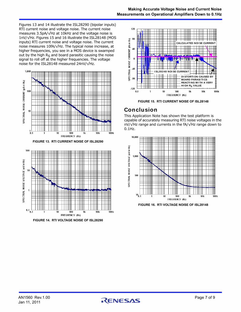
Figures 13 and 14 illustrate the ISL28290 (bipolar inputs) RTI current noise and voltage noise. The current noise measures 3.5pA/√Hz at 10kHz and the voltage noise is 1nV/√Hz. Figures 15 and 16 illustrate the ISL28148 (MOS inputs) RTI current noise and voltage noise. The current noise measures 10fA/√Hz. The typical noise increase, at higher frequencies, you see in a MOS device is swamped out by the high RS and board parasitic causing the noise signal to roll off at the higher frequencies. The voltage noise for the ISL28148 measured 24nV/√Hz.
ConclusionThis Application Note has shown the test platform is capable of accurately measuring RTI noise voltages in the nV/√Hz range and currents in the fA/√Hz range down to 0.1Hz.
FIGURE 13. RTI CURRENT NOISE OF ISL28290
FIGURE 14. RTI VOLTAGE NOISE OF ISL28290
DISTORTION CAUSED BYBOARD PARASITICSREACTING WITH A VERYHIGH RS VALUE
CALCULATED NOISE CURRENT
ISL28248 NOISE CURRENT
FIGURE 15. RTI CURRENT NOISE OF ISL28148
FIGURE 16. RTI VOLTAGE NOISE OF ISL28148
AN1560 Rev.1.00 Page 7 of 9Jan 11, 2011

Making Accurate Voltage Noise and Current Noise
Measurements on Operational Amplifiers Down to 0.1Hz
Things Learned Along the Way1. The Post amplifier is necessary to improve the
effective system noise floor of the DSA.2. Measuring voltage noise of a device below 3 nV/√Hz
can be accomplished by gaining up the DUT. The gain of the DUT lowers the contribution of the PA-DSA noise. This gain should be just enough to enable the measurement of the DUT’s noise at 0.1Hz.
3. The Faraday cage provides another decade of frequency with a noise floor of 3nV/√Hz in the flat band range. This is critical for low frequency noise measurements.
4. The internal AC coupling of the DSA is inadequate for measurements below 1Hz.
5. The external AC coupling network results in having to account for the long time constant before accurate measurements could be made.
6. The series resistor used in the measurement of current noise needs to be as large as possible. The product of RS
2 In2 magnitude needs to be high enough to raise it above background noise and make it a measurable signal. Suggested starting point is to make RS
2 In2 >= 4kTRS.7. Current noise measurements in the femto amps require
sufficient averaging to be able smooth out the data.
References[1] Felice Crupi, Gino Giusi, Carmine Ciofi, Member,
IEEE, and Calogero Pace, “Enhanced Sensitivity Cross Correlation Method for Voltage Noise Measurements”, IEEE Transactions on Instrumentation and Measurement, Vol. 55, No. 4, August 2006.
[2] Paul Lee, Application Note AN-940, “Low Noise Amplifier Selection Guide for Optimal Noise Performance”, Analog Devices
[3] Application Note AN519.1, “Operational Amplifier Noise Prediction (All Op Amps)”, Intersil Corporation, November 1996 .
[4] Derek F. Bowers, IEEE 1989, “Minimizing Noise in Analog Bipolar Circuit Design”, Precision Monolithics, Inc.
[5] Art Kay, “Analysis and Measurement of Intrinsic Noise in Op Amp Circuits Part II Introduction to Opamp Noise”, Texas Instruments Inc.
AN1560 Rev.1.00 Page 8 of 9Jan 11, 2011

http://www.renesas.comRefer to "http://www.renesas.com/" for the latest and detailed information.
Renesas Electronics America Inc.1001 Murphy Ranch Road, Milpitas, CA 95035, U.S.A.Tel: +1-408-432-8888, Fax: +1-408-434-5351Renesas Electronics Canada Limited9251 Yonge Street, Suite 8309 Richmond Hill, Ontario Canada L4C 9T3Tel: +1-905-237-2004Renesas Electronics Europe LimitedDukes Meadow, Millboard Road, Bourne End, Buckinghamshire, SL8 5FH, U.KTel: +44-1628-651-700, Fax: +44-1628-651-804Renesas Electronics Europe GmbHArcadiastrasse 10, 40472 Düsseldorf, Germany Tel: +49-211-6503-0, Fax: +49-211-6503-1327Renesas Electronics (China) Co., Ltd.Room 1709 Quantum Plaza, No.27 ZhichunLu, Haidian District, Beijing, 100191 P. R. ChinaTel: +86-10-8235-1155, Fax: +86-10-8235-7679Renesas Electronics (Shanghai) Co., Ltd.Unit 301, Tower A, Central Towers, 555 Langao Road, Putuo District, Shanghai, 200333 P. R. China Tel: +86-21-2226-0888, Fax: +86-21-2226-0999Renesas Electronics Hong Kong LimitedUnit 1601-1611, 16/F., Tower 2, Grand Century Place, 193 Prince Edward Road West, Mongkok, Kowloon, Hong KongTel: +852-2265-6688, Fax: +852 2886-9022Renesas Electronics Taiwan Co., Ltd.13F, No. 363, Fu Shing North Road, Taipei 10543, TaiwanTel: +886-2-8175-9600, Fax: +886 2-8175-9670Renesas Electronics Singapore Pte. Ltd.80 Bendemeer Road, Unit #06-02 Hyflux Innovation Centre, Singapore 339949Tel: +65-6213-0200, Fax: +65-6213-0300Renesas Electronics Malaysia Sdn.Bhd.Unit 1207, Block B, Menara Amcorp, Amcorp Trade Centre, No. 18, Jln Persiaran Barat, 46050 Petaling Jaya, Selangor Darul Ehsan, MalaysiaTel: +60-3-7955-9390, Fax: +60-3-7955-9510Renesas Electronics India Pvt. Ltd.No.777C, 100 Feet Road, HAL 2nd Stage, Indiranagar, Bangalore 560 038, IndiaTel: +91-80-67208700, Fax: +91-80-67208777Renesas Electronics Korea Co., Ltd.17F, KAMCO Yangjae Tower, 262, Gangnam-daero, Gangnam-gu, Seoul, 06265 KoreaTel: +82-2-558-3737, Fax: +82-2-558-5338
SALES OFFICES
© 2018 Renesas Electronics Corporation. All rights reserved.Colophon 7.0
(Rev.4.0-1 November 2017)
Notice
1. Descriptions of circuits, software and other related information in this document are provided only to illustrate the operation of semiconductor products and application examples. You are fully responsible for
the incorporation or any other use of the circuits, software, and information in the design of your product or system. Renesas Electronics disclaims any and all liability for any losses and damages incurred by
you or third parties arising from the use of these circuits, software, or information.
2. Renesas Electronics hereby expressly disclaims any warranties against and liability for infringement or any other claims involving patents, copyrights, or other intellectual property rights of third parties, by or
arising from the use of Renesas Electronics products or technical information described in this document, including but not limited to, the product data, drawings, charts, programs, algorithms, and application
examples.
3. No license, express, implied or otherwise, is granted hereby under any patents, copyrights or other intellectual property rights of Renesas Electronics or others.
4. You shall not alter, modify, copy, or reverse engineer any Renesas Electronics product, whether in whole or in part. Renesas Electronics disclaims any and all liability for any losses or damages incurred by
you or third parties arising from such alteration, modification, copying or reverse engineering.
5. Renesas Electronics products are classified according to the following two quality grades: “Standard” and “High Quality”. The intended applications for each Renesas Electronics product depends on the
product’s quality grade, as indicated below.
"Standard": Computers; office equipment; communications equipment; test and measurement equipment; audio and visual equipment; home electronic appliances; machine tools; personal electronic
equipment; industrial robots; etc.
"High Quality": Transportation equipment (automobiles, trains, ships, etc.); traffic control (traffic lights); large-scale communication equipment; key financial terminal systems; safety control equipment; etc.
Unless expressly designated as a high reliability product or a product for harsh environments in a Renesas Electronics data sheet or other Renesas Electronics document, Renesas Electronics products are
not intended or authorized for use in products or systems that may pose a direct threat to human life or bodily injury (artificial life support devices or systems; surgical implantations; etc.), or may cause
serious property damage (space system; undersea repeaters; nuclear power control systems; aircraft control systems; key plant systems; military equipment; etc.). Renesas Electronics disclaims any and all
liability for any damages or losses incurred by you or any third parties arising from the use of any Renesas Electronics product that is inconsistent with any Renesas Electronics data sheet, user’s manual or
other Renesas Electronics document.
6. When using Renesas Electronics products, refer to the latest product information (data sheets, user’s manuals, application notes, “General Notes for Handling and Using Semiconductor Devices” in the
reliability handbook, etc.), and ensure that usage conditions are within the ranges specified by Renesas Electronics with respect to maximum ratings, operating power supply voltage range, heat dissipation
characteristics, installation, etc. Renesas Electronics disclaims any and all liability for any malfunctions, failure or accident arising out of the use of Renesas Electronics products outside of such specified
ranges.
7. Although Renesas Electronics endeavors to improve the quality and reliability of Renesas Electronics products, semiconductor products have specific characteristics, such as the occurrence of failure at a
certain rate and malfunctions under certain use conditions. Unless designated as a high reliability product or a product for harsh environments in a Renesas Electronics data sheet or other Renesas
Electronics document, Renesas Electronics products are not subject to radiation resistance design. You are responsible for implementing safety measures to guard against the possibility of bodily injury, injury
or damage caused by fire, and/or danger to the public in the event of a failure or malfunction of Renesas Electronics products, such as safety design for hardware and software, including but not limited to
redundancy, fire control and malfunction prevention, appropriate treatment for aging degradation or any other appropriate measures. Because the evaluation of microcomputer software alone is very difficult
and impractical, you are responsible for evaluating the safety of the final products or systems manufactured by you.
8. Please contact a Renesas Electronics sales office for details as to environmental matters such as the environmental compatibility of each Renesas Electronics product. You are responsible for carefully and
sufficiently investigating applicable laws and regulations that regulate the inclusion or use of controlled substances, including without limitation, the EU RoHS Directive, and using Renesas Electronics
products in compliance with all these applicable laws and regulations. Renesas Electronics disclaims any and all liability for damages or losses occurring as a result of your noncompliance with applicable
laws and regulations.
9. Renesas Electronics products and technologies shall not be used for or incorporated into any products or systems whose manufacture, use, or sale is prohibited under any applicable domestic or foreign laws
or regulations. You shall comply with any applicable export control laws and regulations promulgated and administered by the governments of any countries asserting jurisdiction over the parties or
transactions.
10. It is the responsibility of the buyer or distributor of Renesas Electronics products, or any other party who distributes, disposes of, or otherwise sells or transfers the product to a third party, to notify such third
party in advance of the contents and conditions set forth in this document.
11. This document shall not be reprinted, reproduced or duplicated in any form, in whole or in part, without prior written consent of Renesas Electronics.
12. Please contact a Renesas Electronics sales office if you have any questions regarding the information contained in this document or Renesas Electronics products.
(Note 1) “Renesas Electronics” as used in this document means Renesas Electronics Corporation and also includes its directly or indirectly controlled subsidiaries.
(Note 2) “Renesas Electronics product(s)” means any product developed or manufactured by or for Renesas Electronics.