an243 application note - farnell.com · pin function of the l294 ... enable. ttl-compatible logic...
TRANSCRIPT
November 2006 Rev 2 1/17
AN243Application note
Swith-mode drivers for solenoid driving
OverviewMany applications, particularly in computer peripherals, require a high power, fast solenoid driver circuit. In the past these circuits have been released with discrete components because the high powers required precluded the use of monolithic technology. STMicroelectronics has overcome this problem with a new high power bipolar technology that uses an innovative implanted isolation technique.
This technology is used to fabricate two switchmode solenoid driver chips, the L294 and L295, which both incorporate high power output stages and control circuitry. Both circuits are designed for efficient switchmode operation and are mounted in a Multiwatt plastic package.
www.st.com

Contents AN243
2/17
Contents
1 The L294 solenoid driver . . . . . . . . . . . . . . . . . . . . . . . . . . . . . . . . . . . . . 2
1.1 Circuit operation . . . . . . . . . . . . . . . . . . . . . . . . . . . . . . . . . . . . . . . . . . . . . 2
1.2 Protection . . . . . . . . . . . . . . . . . . . . . . . . . . . . . . . . . . . . . . . . . . . . . . . . . . 4
2 Using the L294 . . . . . . . . . . . . . . . . . . . . . . . . . . . . . . . . . . . . . . . . . . . . . . 5
2.1 The L295 dual switchmode driver . . . . . . . . . . . . . . . . . . . . . . . . . . . . . . . 8
3 Inside the L295 . . . . . . . . . . . . . . . . . . . . . . . . . . . . . . . . . . . . . . . . . . . . . 9
3.1 Two level control . . . . . . . . . . . . . . . . . . . . . . . . . . . . . . . . . . . . . . . . . . . . 10
4 L295 application hints . . . . . . . . . . . . . . . . . . . . . . . . . . . . . . . . . . . . . . . 12
5 Revision history . . . . . . . . . . . . . . . . . . . . . . . . . . . . . . . . . . . . . . . . . . . 15

AN243 The L294 solenoid driver
3/17
1 The L294 solenoid driver
The L294 is designed for solenoid driving applications where both very high speed and high current are essential; needle and hammer driving in printer mechanisms, for example. It delivers 4A with supply voltages up to 46V, handling effective powers up to 180W.
Figure 1. Internal block diagram of the L294 switchmode solenoid driver.
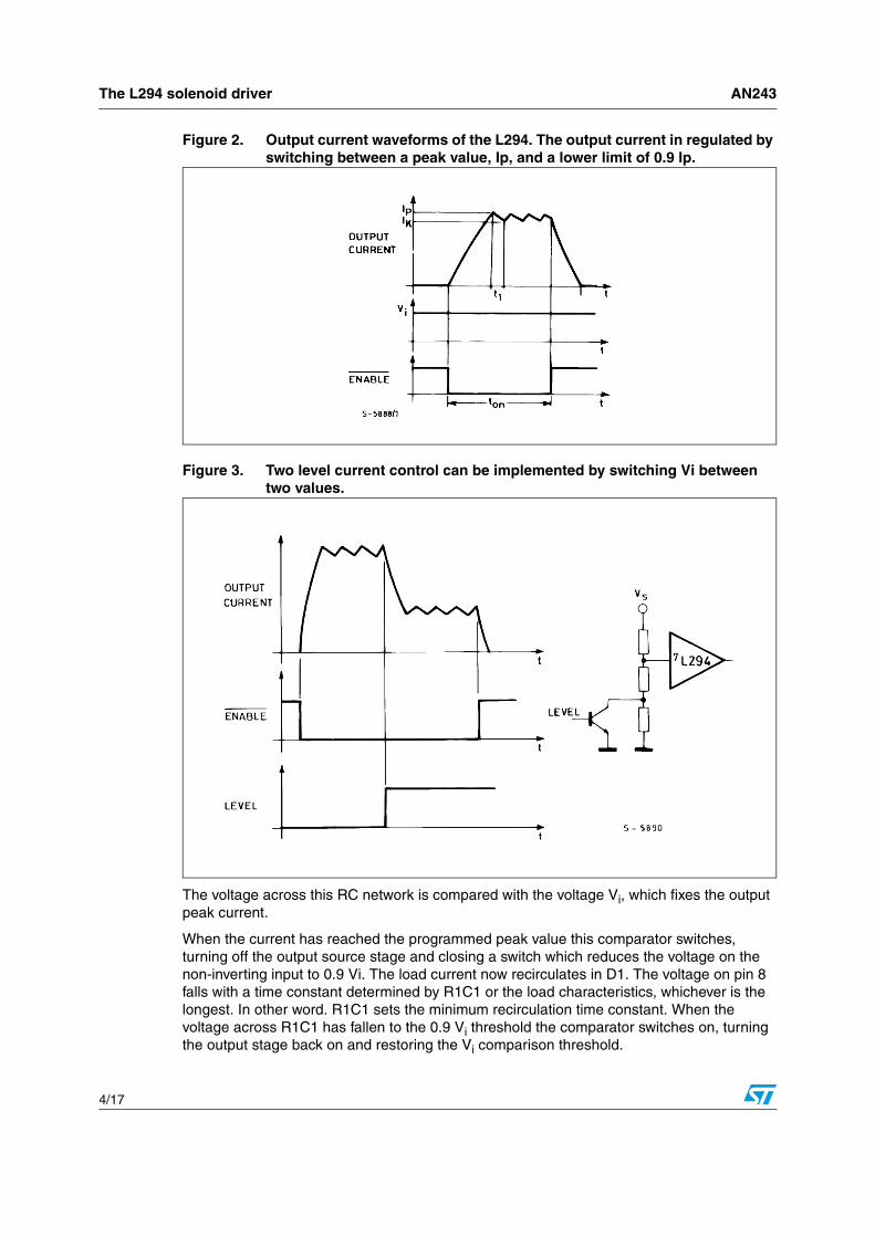
Shown in figure 1, the L294 is controlled by a TTL - level logic input and the peak load current is programmed by a reference voltage applied to the pin labelled Vi. Internal switchmode control circuitry regulates the solenoid current by turning the output stage on and off repeatedly to keep the load current between the programmed peak value, Ip, and a lower limit of 0.9 Ip.
Other features of the L294 include thermal shutdown, output short circuit protection, overdriving protection and a latched diagnostic output. This output indicates fault conditions such as a short circuit solenoid.
1.1 Circuit operationIn most applications the L294 is used with a fixed reference voltage (Vi) and the solenoid is controlled by negative-going pulses on the ENABLE input. When the ENABLE input is active (low level), the output stage is enabled and the load current rises as shown in figure 2.
The load current is sensed by an external resistor (Rs) in the emitter of the sink stage. Through the op amp and transconductance amplifier (OTA), the sensed voltage charges an external RC network (R1C1) which determines the switching characteristics of the device.
The L294 solenoid driver AN243
4/17
Figure 2. Output current waveforms of the L294. The output current in regulated by switching between a peak value, Ip, and a lower limit of 0.9 Ip.
Figure 3. Two level current control can be implemented by switching Vi between two values.
The voltage across this RC network is compared with the voltage Vi, which fixes the output peak current.
When the current has reached the programmed peak value this comparator switches, turning off the output source stage and closing a switch which reduces the voltage on the non-inverting input to 0.9 Vi. The load current now recirculates in D1. The voltage on pin 8 falls with a time constant determined by R1C1 or the load characteristics, whichever is the longest. In other word. R1C1 sets the minimum recirculation time constant. When the voltage across R1C1 has fallen to the 0.9 Vi threshold the comparator switches on, turning the output stage back on and restoring the Vi comparison threshold.

AN243 The L294 solenoid driver
5/17
The output source stage is switched in this way, regulating the load current, until the ENABLE input goes high again. At this point the output stage is disabled - both source and sink - and the load current recirculates through D1 and D2 to ensure a fast decay. By varying the voltage Vi the peak load current can be programmed to any value in the range 0.6A to 4A. This feature can be exploited to implement two-level current control if the fixed reference is replaced by a switched reference as shown in figure 3.
1.2 ProtectionTo protect the load and the L294 from overdriving an on-time limiter inhibits the output stage independently of the ENABLE input if the duration of the input pulse exceeds a period set by the external capacitor C2 (figure 4). This circuit is reset by taking the ENABLE input high. The on-time limiter can be disabled by grounding pin 3.
Figure 4. On–time limiter waveforms. after a period defined by C2, the output is disabled regardless of the state of ENABLE, protecting against overdriving.
Protection against overheating is incorporated in the form of a thermal shutdown circuit which disables the output stage when the junction temperature exceeds 150°C. The circuit restarts when the temperature has fallen about 20°C. The L294 is also protected against short circuits to ground, to supply and across the load. Triggered when the source stage current exceed 5A or the sink stage current exceed 1 V/RS, the short circuit protection block inhibits the output stage and sets a flip flop which is supplied by a separate supply voltage VSS. This flip flop is connected to the diagnostic output and signals that all is not well - a shorted solenoid, for example. The diagnostic flip flop is reset by removing the supply VS.
A LED can be connected to the diagnostic output as shown in figure 5. If the diagnostic function is not required the VSS supply can be omitted. The short circuit protection, however, still functions, even without VSS.

Using the L294 AN243
6/17
2 Using the L294
The basic application circuit for the L294 is shown in figure 5; a suggested layout is given in figure 6. The circuit is complete except for the source of Vi. In most cases this will be provided by a simple resistive divider dimensioned to set the desired peak current. With a 0.2W sense resistor as shown, the L294 has a transconductance of 1A/V for Vi above 600 mV. The device will not work with Vi less than 450 mV and operation is not guaranteed for Vi between 450 mV and 600 mV. The on-time limiter delay, set by C2, is approximately 120000 x C2. Pin 3 must be grounded if the ontime limiter isn’t used.
Switching frequency depends partly on the timing network R1C1 and partly on the load characteristics. R1C1 determines the minimum value of t1 (see figure 2), which is given by t1 > 0.1 x R1C1. C1 must be in the range 2.7 - 10 nF to ensure stability of the amplifier OTA. R1 must be at least 10kΩ to give sufficient gain for OTA. The standard application circuit of figure 5 has a switching frequency of about 10 kHz.
The recirculation diodes should be fast types and rated at 3A (D1) and 1A (D2). If the full 4A capability of the L294 is not used these can be reduced.
Figure 5. Standard solenoid driving application of the L294. Pin 7 must be connected to suitable reference voltage to set the peak current.

AN243 Using the L294
7/17
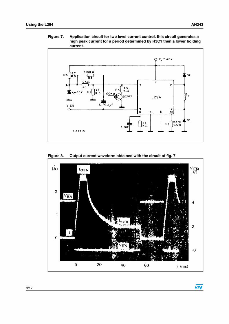
A high initial peak and low holding current can be obtained with the circuit shown in figure 7a. This example supplies a current peak for about 10 ms.
The peak current, IOEX, (see figure 7a) is found from:
Vz is the zener voltage. The zener and R5 can be omitted if a regulated 5 V supply is available for point A.
The holding current, Ihold, is found from:
:
Figure 6. Suggested printed circuit board laypout for the application circuit of figure 5.
Table 1. The duration of the peak is determined by R3C1 and is increased by raising R3 or C1. Typical component values are listed in the table below
+IOEX = 4A; IHOLD = 1 A +IOEX = 2.5A; IHOLD = 0.5 A
R1 10 kΩ 10 kΩ
R2 47 kΩ 27 kΩ
R3 150 kΩ 150 kΩ
R4 2.7 kΩ 1.5 kΩ
R5 0.2 Ω (1W) 0.27 Ω (0.5W)
D1 3 A 1.5 A
D2 0.5 A 0.5 A
C1 0.2 μF 0.2 μF
IOEX
Vz5------ R2
RS-------- 1
R1 R2+----------------------⋅ ⋅=
Ihold
Vz5------ R2//R4( )
RS------------------------ 1
R1 R2//R4( )+---------------------------------------⋅ ⋅=
Using the L294 AN243
8/17
Figure 7. Application circuit for two level current control. this circuit generates a high peak current for a period determined by R3C1 then a lower holding current.
Figure 8. Output current waveform obtained with the circuit of fig. 7

AN243 Using the L294
9/17
2.1 The L295 dual switchmode driverThe L295 is a dual switchmode solenoid driver which handles up to 2.5A per channel at voltages up to 46V - a total effective power handling of 220W. Compared to the L294 it offers a more economical solution when 2.5A is sufficient because there are two drivers per chip. Like the L294 it features switchmode regulation of the output current and hermal shutdown. Additionally it has a separate logic supply input so that the logic can be run at a lowervoltage, reducing dissipation.
Intended for inductive load driving, the L295 is particularly suitable for solenoids and stepper motors. One L295 drives two solenoids and two L295s can drive the four phases at a unipolar stepper motor or the two phases of a bipolar stepper motor in bridge configuration. Each channel of the L295 is controlled by a TTL-level digital input and the peak load current is programmed, independently for each channel, by a voltage reference input. A chip enable input is also provided to disable both channels together.
Table 2. Pin Function Of The L294
N Function
1 Solenoid Supply Voltage Vs (12-46V)
2 Output, Source Stage
3On-time Limiter Time Constant. A capacitor to ground sets delay period (120000 x C2 seconds). On-time limiter is disabled by grounding this pin
4 Supply Input (5V) for Diagnostic Flip Flop.
5Diagnostic Output, Open Collector. Signals intervention of latched short circuit protection. Reset by removing pin 1 supply
6 Ground.
7Vi Reference Input. Peak output current is proportional to Vi.
Transconductance is 1A/V for RS = 0.2 Ω and Vi ≥ 600 mV.
8Timing. A parallel RC network from this pin to ground sets the minimum recirculation time constant. The capacitor must be 2.7-10 nF to ensure stability.
The resistor must be greater than 10 kΩ
9ENABLE. TTL-compatible logic input that controls the solenoid current. The solenoid is driven when this input is at a low level. The on-time limiter overrides enable.
10 Connection for Load Current Sense Resistor.
11 Output, Sink Stage
Inside the L295 AN243
10/17
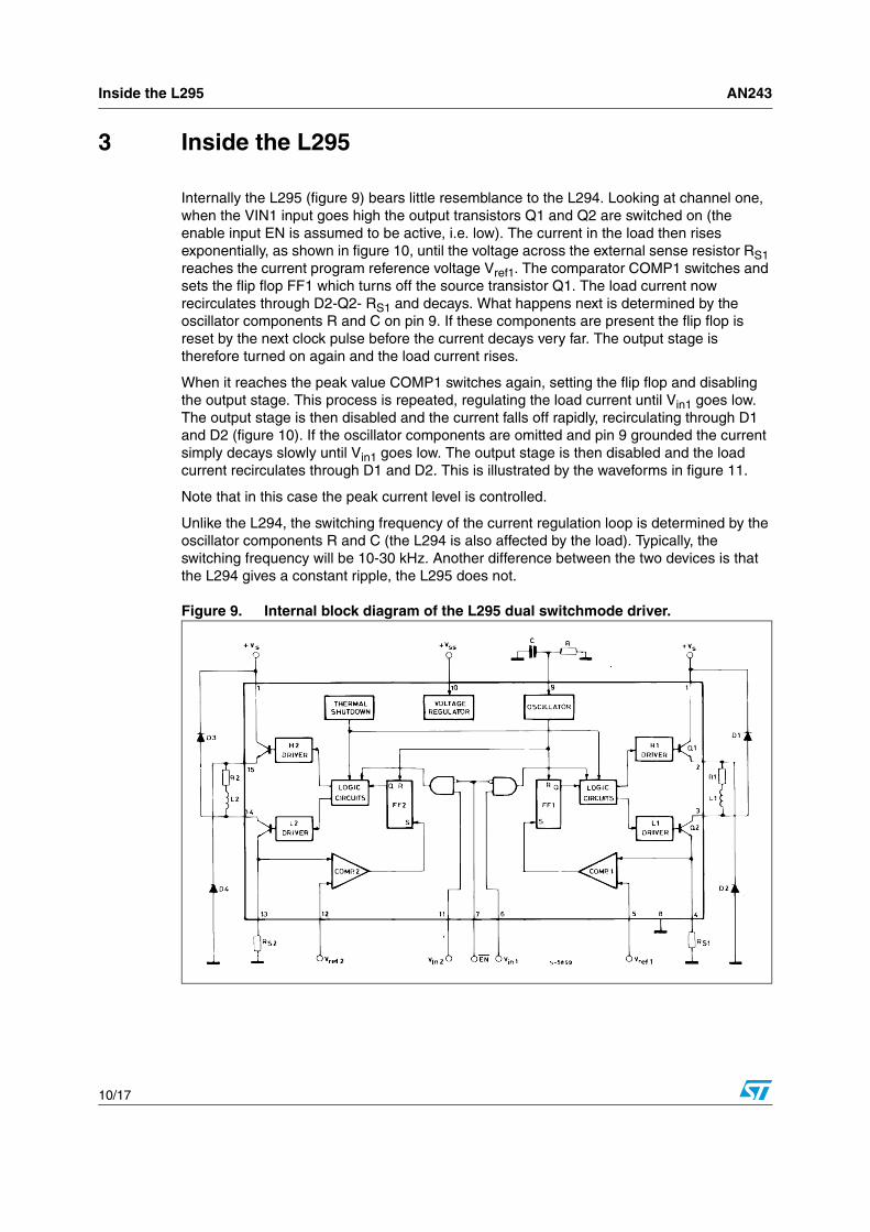
3 Inside the L295
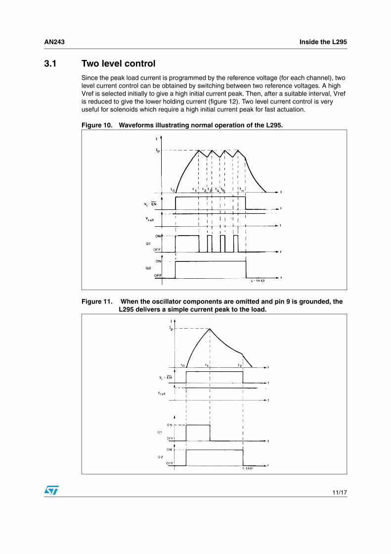
Internally the L295 (figure 9) bears little resemblance to the L294. Looking at channel one, when the VIN1 input goes high the output transistors Q1 and Q2 are switched on (the enable input EN is assumed to be active, i.e. low). The current in the load then rises exponentially, as shown in figure 10, until the voltage across the external sense resistor RS1 reaches the current program reference voltage Vref1. The comparator COMP1 switches and sets the flip flop FF1 which turns off the source transistor Q1. The load current now recirculates through D2-Q2- RS1 and decays. What happens next is determined by the oscillator components R and C on pin 9. If these components are present the flip flop is reset by the next clock pulse before the current decays very far. The output stage is therefore turned on again and the load current rises.
When it reaches the peak value COMP1 switches again, setting the flip flop and disabling the output stage. This process is repeated, regulating the load current until Vin1 goes low. The output stage is then disabled and the current falls off rapidly, recirculating through D1 and D2 (figure 10). If the oscillator components are omitted and pin 9 grounded the current simply decays slowly until Vin1 goes low. The output stage is then disabled and the load current recirculates through D1 and D2. This is illustrated by the waveforms in figure 11.
Note that in this case the peak current level is controlled.
Unlike the L294, the switching frequency of the current regulation loop is determined by the oscillator components R and C (the L294 is also affected by the load). Typically, the switching frequency will be 10-30 kHz. Another difference between the two devices is that the L294 gives a constant ripple, the L295 does not.
Figure 9. Internal block diagram of the L295 dual switchmode driver.
AN243 Inside the L295
11/17
3.1 Two level controlSince the peak load current is programmed by the reference voltage (for each channel), two level current control can be obtained by switching between two reference voltages. A high Vref is selected initially to give a high initial current peak. Then, after a suitable interval, Vref is reduced to give the lower holding current (figure 12). Two level current control is very useful for solenoids which require a high initial current peak for fast actuation.
Figure 10. Waveforms illustrating normal operation of the L295.
Figure 11. When the oscillator components are omitted and pin 9 is grounded, the L295 delivers a simple current peak to the load.

Inside the L295 AN243
12/17
Figure 12. Two level current control is obtained by switching Vref between two values.
AN243 L295 application hints
13/17
4 L295 application hints
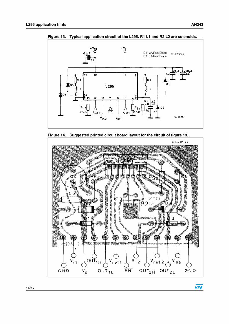
The basic application circuit of the L295 is shown in figure 14. A layout is given in figure 15. Suitable values for the oscillator components, R and C, can be found within figure 16.
The value for the reference voltages depends on the desired peak current and is equal to IpRs; it must be in the range 0.2V to 2V.
If the Vref inputs are left open circuit the L295 assumes an internal default value of 2.5V giving a peak current of 2.5/RS amperes.
The L295 can also be used to drive unipolar stepper motors. For a four phase motor two devices are used, connected as shown in figure 17.
This circuit provides switchmode regulation of the load current with a chopper rate of about 25 kHz. The enable inputs (EN, connected together) enable/disable the whole circuit and the channel inputs Vin1 . . . Vin4 are driven by a suitable translator circuit. Phases 1 and 2 must not be energised together because they share the same sense resistor.
The same applies to channels 3 and 4. However, a two phase on, drive is still possible for bifilar motors where phases one and two represent one winding and 3 & 4 the other, and also for variable reluctance motors with phase 1 adjacent to phase 3 etc.
Two L295s could also be used to drive a bipolar stepper motor in systems where a translator already exists.
.Table 3. Pin Functions of the L295
N° Function
1 Solenoid Supply Voltage, Vs (12-46V).
2 Channel one Output, Source Stage.
3 Channel one Output, Sink Stage.
4 RS1. Sense Resistor Connection, Channel one.
5Vref1. A voltage on this pin sets peak current of channel one. If this pin is left open or connected to Vss a default Vref of 2.5V is assumed. An externally applied Vref must be in the range 0.2 to 2V.
6 Vin1. Logic Input for Channel one. Driver is active when Vin1 is high and EN low.
7 EN. Chip Enable (active low). When high both channels are disabled.
8 Ground.
9 Oscillator Timing Network. This pin is grounded to produce a single peak.
10 Vss. Logic supply voltage, internally regulated. (4.75-10V).
11 Vin2. Logic Input for Channel two. Driver is active when Vin2 is high and EN low.
12Vref2. Voltage input, controls peak current of channel two. If left open or connected Vs an internal 2.5V reference is assumed. An externally applied Vref must be in the range 0.2 to 2V.
13 RS2. Sense Resistor Connection, Channel two.
14 Channel two Output, Sink Stage.
15 Channel two Output, Source Stage.
L295 application hints AN243
14/17
Figure 13. Typical application circuit of the L295. R1 L1 and R2 L2 are solenoids.
Figure 14. Suggested printed circuit board layout for the circuit of figure 13.

AN243 L295 application hints
15/17
Figure 15. Nomogram for the selection of values for the oscillator components. RC.
Figure 16. Two L295s, connected as shown, can be used to drive a four phase unipolar stepper motor.

Revision history AN243
16/17
5 Revision history
Table 4. Document revision history
Date Revision Changes
24-Jan-2006 1 Initial release.
15-Nov-2006 2 Layout changes. Text modifications.

AN243
17/17
Please Read Carefully:
Information in this document is provided solely in connection with ST products. STMicroelectronics NV and its subsidiaries (“ST”) reserve theright to make changes, corrections, modifications or improvements, to this document, and the products and services described herein at anytime, without notice.
All ST products are sold pursuant to ST’s terms and conditions of sale.
Purchasers are solely responsible for the choice, selection and use of the ST products and services described herein, and ST assumes noliability whatsoever relating to the choice, selection or use of the ST products and services described herein.
No license, express or implied, by estoppel or otherwise, to any intellectual property rights is granted under this document. If any part of thisdocument refers to any third party products or services it shall not be deemed a license grant by ST for the use of such third party productsor services, or any intellectual property contained therein or considered as a warranty covering the use in any manner whatsoever of suchthird party products or services or any intellectual property contained therein.
UNLESS OTHERWISE SET FORTH IN ST’S TERMS AND CONDITIONS OF SALE ST DISCLAIMS ANY EXPRESS OR IMPLIEDWARRANTY WITH RESPECT TO THE USE AND/OR SALE OF ST PRODUCTS INCLUDING WITHOUT LIMITATION IMPLIEDWARRANTIES OF MERCHANTABILITY, FITNESS FOR A PARTICULAR PURPOSE (AND THEIR EQUIVALENTS UNDER THE LAWSOF ANY JURISDICTION), OR INFRINGEMENT OF ANY PATENT, COPYRIGHT OR OTHER INTELLECTUAL PROPERTY RIGHT.
UNLESS EXPRESSLY APPROVED IN WRITING BY AN AUTHORIZED ST REPRESENTATIVE, ST PRODUCTS ARE NOTRECOMMENDED, AUTHORIZED OR WARRANTED FOR USE IN MILITARY, AIR CRAFT, SPACE, LIFE SAVING, OR LIFE SUSTAININGAPPLICATIONS, NOR IN PRODUCTS OR SYSTEMS WHERE FAILURE OR MALFUNCTION MAY RESULT IN PERSONAL INJURY,DEATH, OR SEVERE PROPERTY OR ENVIRONMENTAL DAMAGE. ST PRODUCTS WHICH ARE NOT SPECIFIED AS "AUTOMOTIVEGRADE" MAY ONLY BE USED IN AUTOMOTIVE APPLICATIONS AT USER’S OWN RISK.
Resale of ST products with provisions different from the statements and/or technical features set forth in this document shall immediately voidany warranty granted by ST for the ST product or service described herein and shall not create or extend in any manner whatsoever, anyliability of ST.
ST and the ST logo are trademarks or registered trademarks of ST in various countries.
Information in this document supersedes and replaces all information previously supplied.
The ST logo is a registered trademark of STMicroelectronics. All other names are the property of their respective owners.
© 2006 STMicroelectronics - All rights reserved
STMicroelectronics group of companies
Australia - Belgium - Brazil - Canada - China - Czech Republic - Finland - France - Germany - Hong Kong - India - Israel - Italy - Japan - Malaysia - Malta - Morocco - Singapore - Spain - Sweden - Switzerland - United Kingdom - United States of America
www.st.com