an4759, boot loader implementation on mc56f84xxx dsc ...boot loader implementation on mc56f84xxx dsc...
TRANSCRIPT
Freescale Semiconductor Document Number: AN4759 Application Note Rev. 0, 06/2013
© 2013 Freescale Semiconductor, Inc.
_______________________________________________________________________
Boot Loader Implementation on
MC56F84xxx DSC Family by: Xuwei Zhou
1 Introduction
Many applications require a piece of codes
called boot loader residing in the nonvolatile
memory besides the application codes. The boot
loader is completely independent of the
application codes, and its main function is to
communicate with a host to get the updated
application codes and program the codes into
the application codes area of nonvolatile
memory on the chip. In MC56F84xxx digital
signal controller (DSC) series, flash is the
nonvolatile memory and it’s different from the
flash memory in the earlier DSC series.
This application note aims to explain every
detail of how to implement a boot loader on
DSCs of MC56F84xxx series, taking
MC56F84789 as an example. CodeWarrior10.3
with Processer Expert (PE) is used as the
development environment.
Contents 1 Introduction ......................................................1
2 Boot loader mechanism ....................................2
2.1 Memory map in MC56F84789 DSC ........2
2.2 Memory configuration for boot loader .....3
3 Boot loader implementation .............................6
3.1 S-record for DSC series ............................6
3.2 Circular buffer ..........................................8
3.3 Boot loader state machine realization .....11
3.4 Decoding of s-record ..............................16
3.5 Erase/program flash memory ..................17
4 Software introduction .....................................20
4.1 Linker file ...............................................20
4.2 The do's and don'ts of implementing the
boot loader ..........................................................23
5 User application requirements ........................24
6 Conclusion ......................................................26
7 References ......................................................26
8 Revision history ..............................................27

Boot Loader Implementation on MC56F84xxx DSC Family, Rev. 0, 06/2013
2 Freescale Semiconductor
2 Boot loader mechanism
When a system is reset, the boot loader code is executed first and decides whether to reprogram the flash
memory or not. If the flash is to be reprogrammed, the system will communicate with a host to receive
the application code and update it. The updated application code will be started when the update is done.
If update is not required, the current application code will be executed after exiting from the boot loader.
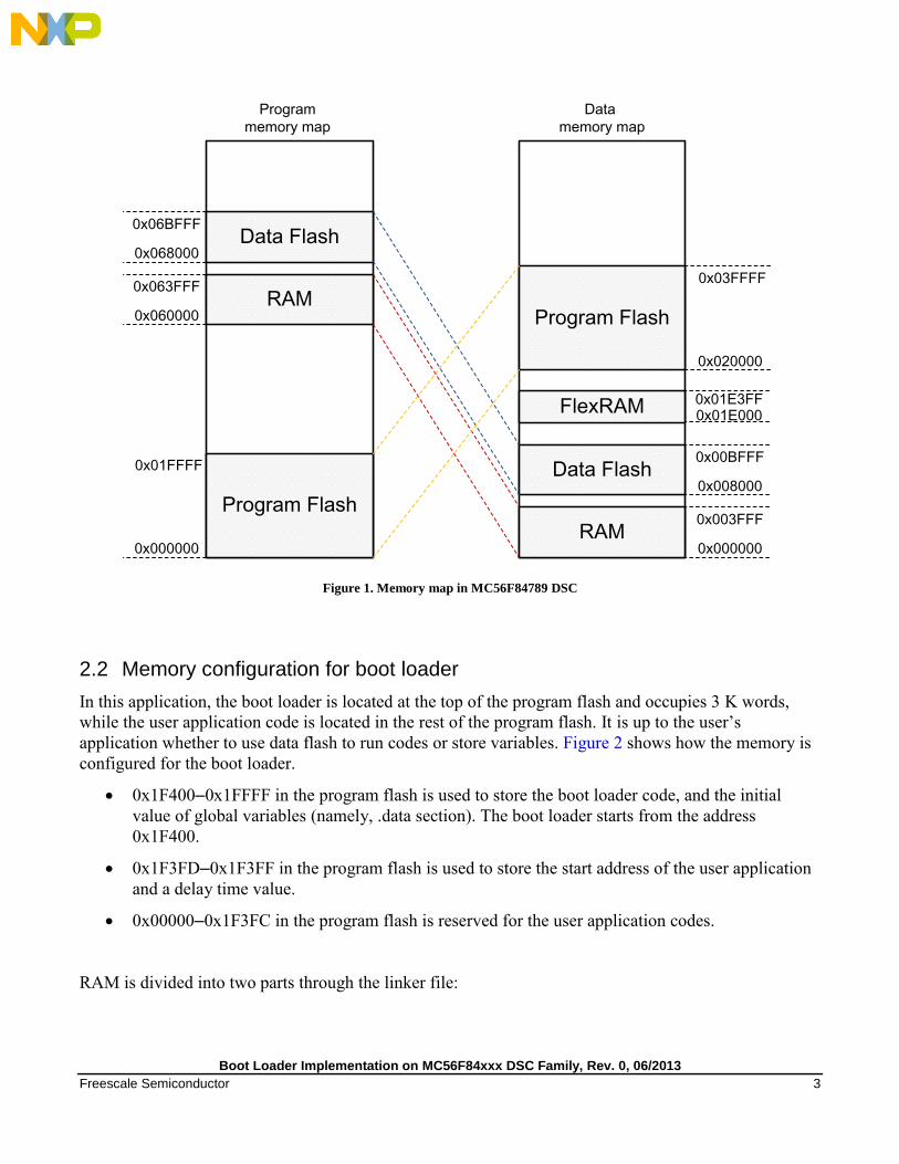
2.1 Memory map in MC56F84789 DSC
It is essential to know the detailed memory map on the MC56F84789 MCU. This information can be
found in Chapter 4 “Memory Map” of MC56F847XXRM: MC56F847xx Reference Manual, available on
freescale.com. As for MC56F84789, there are two pieces of flash memories and two pieces of RAMs
inside the chip. Both the flash memories and one of the RAMs can be accessed through program
memory buses and data memory buses. This means that each of them has two sets of addresses that are
mapped into program memory and data memory. Figure 1 shows the exact memory map of
MC56F84789 MCU.
Note: It is just a convention to refer to these two pieces of flash memories as “program” and “data”
flash.
Program flash:
It has a volume of 128 K words which is relatively large.
It starts from address 0x0000 in the program memory map which makes it more suitable to store
codes.
It can be used to store variables with constant values since it is also mapped into data memory as
indicated in Figure 1.
Data flash:
The same naming rule applies to data flash; the reason it’s called “data” flash is that its volume is
16 K words which is smaller.
It starts from 0x8000 in the data memory map which makes it more suitable to store variables
with constant values.
It can be used to store codes since it is also mapped to program memory.
There’s a RAM of 16 K words mapped into both the program and data memories, so codes can also run
in it. FlexRAM is only mapped into data memory. It can be accessed as traditional RAM or configured
as enhanced EEPROM together with part of the data flash. See AN4689: EEPROM on MC56F84xxx
DSC, available on freescale.com, for EEPROM usage on MC56F84xxx.
Boot Loader Implementation on MC56F84xxx DSC Family, Rev. 0, 06/2013
Freescale Semiconductor 3
Data Flash
Program Flash
RAM
0x000000
0x01FFFF
0x060000
0x063FFF
0x068000
0x06BFFF
Data Flash
Program Flash
RAM
0x020000
0x03FFFF
0x000000
0x003FFF
0x008000
0x00BFFF
FlexRAM0x01E0000x01E3FF
Program
memory map
Data
memory map
Figure 1. Memory map in MC56F84789 DSC
2.2 Memory configuration for boot loader
In this application, the boot loader is located at the top of the program flash and occupies 3 K words,
while the user application code is located in the rest of the program flash. It is up to the user’s
application whether to use data flash to run codes or store variables. Figure 2 shows how the memory is
configured for the boot loader.
0x1F400–0x1FFFF in the program flash is used to store the boot loader code, and the initial
value of global variables (namely, .data section). The boot loader starts from the address
0x1F400.
0x1F3FD–0x1F3FF in the program flash is used to store the start address of the user application
and a delay time value.
0x00000–0x1F3FC in the program flash is reserved for the user application codes.
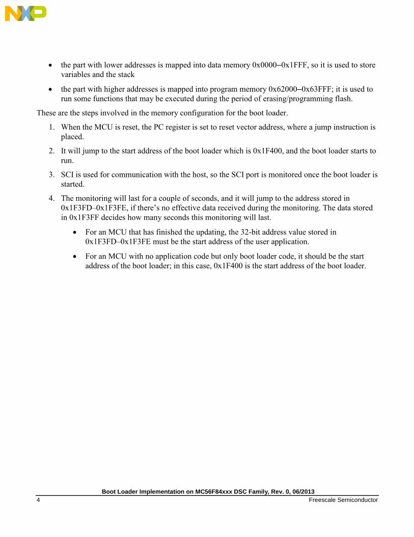
RAM is divided into two parts through the linker file:
Boot Loader Implementation on MC56F84xxx DSC Family, Rev. 0, 06/2013
4 Freescale Semiconductor
the part with lower addresses is mapped into data memory 0x0000–0x1FFF, so it is used to store
variables and the stack
the part with higher addresses is mapped into program memory 0x62000–0x63FFF; it is used to
run some functions that may be executed during the period of erasing/programming flash.
These are the steps involved in the memory configuration for the boot loader.
1. When the MCU is reset, the PC register is set to reset vector address, where a jump instruction is
placed.
2. It will jump to the start address of the boot loader which is 0x1F400, and the boot loader starts to
run.
3. SCI is used for communication with the host, so the SCI port is monitored once the boot loader is
started.
4. The monitoring will last for a couple of seconds, and it will jump to the address stored in
0x1F3FD–0x1F3FE, if there’s no effective data received during the monitoring. The data stored
in 0x1F3FF decides how many seconds this monitoring will last.
For an MCU that has finished the updating, the 32-bit address value stored in
0x1F3FD–0x1F3FE must be the start address of the user application.
For an MCU with no application code but only boot loader code, it should be the start
address of the boot loader; in this case, 0x1F400 is the start address of the boot loader.

Boot Loader Implementation on MC56F84xxx DSC Family, Rev. 0, 06/2013
Freescale Semiconductor 5
0x000000
0x01FFFF
0x062000
0x063FFF
Program
memory map
Data
memory map
Bootloader0x01F400
User app start address0x01F3FD
0x01F3FE
0x01F3FF Delay time
0x01F3FC
User application codes
0x000000
0x0007FF.bss
Global variables0x000800
0x0009FF
Stack and heap0x000A00
0x001FFF
Functions
running in RAM
Program
flash
3Kwords
1 word
2 words
5.5K
words
0.5K
words
2Kwords
8Kwords
RAM
mapped
in data
memory
RAM
mapped
in
program
memory
Figure 2. Memory configuration in MC56F84789 for boot loader
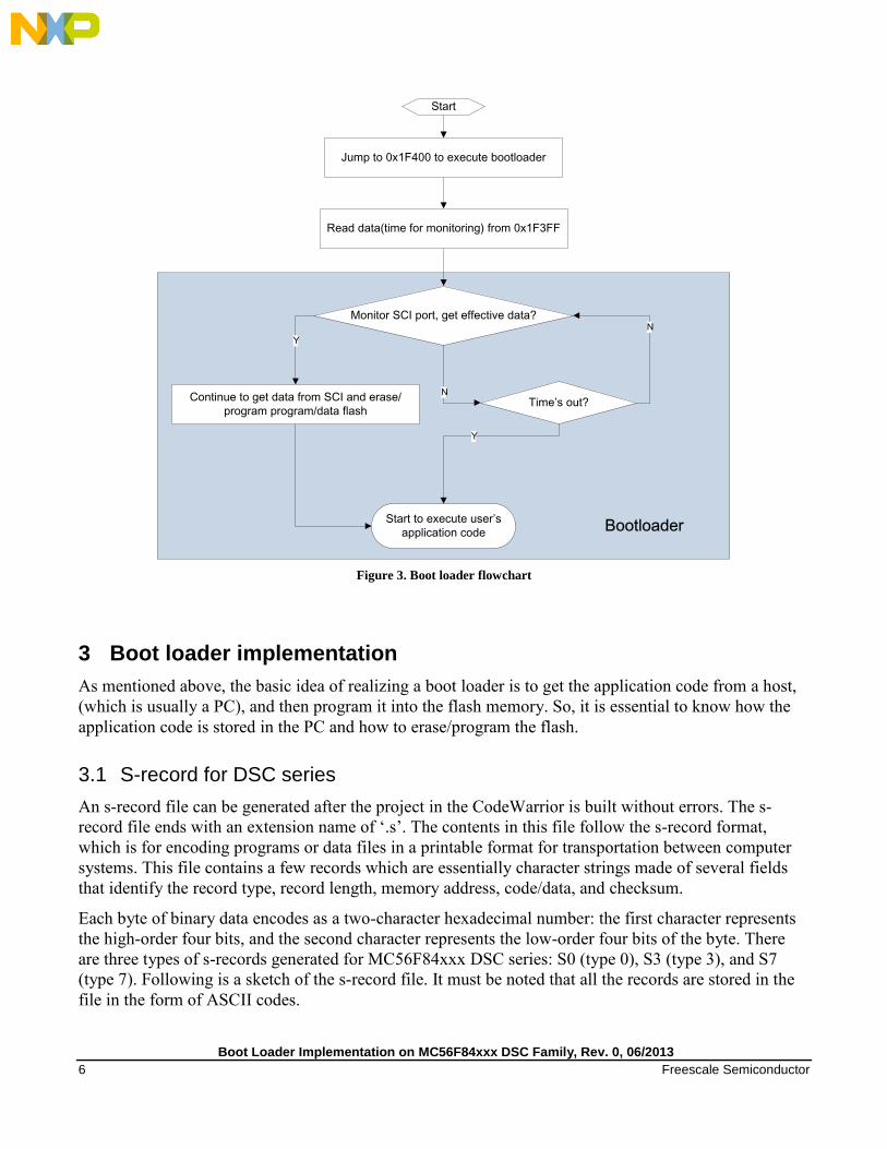
Figure 3 shows the execution flow of the boot loader. If effective data is received during the monitoring,
the boot loader will be carried on and both the non-boot loader program flash and data flash will be
erased and programmed (0x1F400–0x1FFFF in the program flash is excluded).
Boot Loader Implementation on MC56F84xxx DSC Family, Rev. 0, 06/2013
6 Freescale Semiconductor
Start
Jump to 0x1F400 to execute bootloader
Time’s out?
Read data(time for monitoring) from 0x1F3FF
Monitor SCI port, get effective data?
Continue to get data from SCI and erase/
program program/data flash
Start to execute user’s
application code
N
Y
Y
N
Bootloader
Figure 3. Boot loader flowchart
3 Boot loader implementation
As mentioned above, the basic idea of realizing a boot loader is to get the application code from a host,
(which is usually a PC), and then program it into the flash memory. So, it is essential to know how the
application code is stored in the PC and how to erase/program the flash.
3.1 S-record for DSC series
An s-record file can be generated after the project in the CodeWarrior is built without errors. The s-
record file ends with an extension name of ‘.s’. The contents in this file follow the s-record format,
which is for encoding programs or data files in a printable format for transportation between computer
systems. This file contains a few records which are essentially character strings made of several fields
that identify the record type, record length, memory address, code/data, and checksum.
Each byte of binary data encodes as a two-character hexadecimal number: the first character represents
the high-order four bits, and the second character represents the low-order four bits of the byte. There
are three types of s-records generated for MC56F84xxx DSC series: S0 (type 0), S3 (type 3), and S7
(type 7). Following is a sketch of the s-record file. It must be noted that all the records are stored in the
file in the form of ASCII codes.

Boot Loader Implementation on MC56F84xxx DSC Family, Rev. 0, 06/2013
Freescale Semiconductor 7
S0110000000050524F4752414D264441544196
S3150000000054E100F454E100F454E22A0254E22A02D4
S3150000000854E22A0254E22A0254E22A0254E22A025A
S3150000001054E22A0254E22A0254E22A0254E22A0252
S3150000001854E22A0254E22A0254E22A0254E22A024A
… S30B0000F3FD310200000C00C5
S70500000231C7
This figure explains the encoding scheme with appropriate labeling, taking one of the s-records as an
example.
S3150000001854E22A0254E22A0254E22A0254E22A024A
Checksum
Code/Data
Address
Record length
Type
Figure 4. S-record encoding scheme
Type: There are eight types of s-records to accommodate the encoding, transportation, and
decoding functions. But only the following three of them will be generated here.
o S0: It is the header record for each block of s-records. The code/data field may contain
any descriptive information identifying the following block of s-records. The address
field is normally zeros. The S0 record generated in DSC series is: S0110000000050524F4752414D264441544196
The code/data field “50524F4752414D2644415441” is actually the ASCII code of
“PROGRAM&DATA”.
o S3: This record contains code/data and the 32-bit start word address at which the
code/data is to reside.
o S7: It is a termination record for a block of S3 records. The address field may optionally
contain the 32-bit word address of the instruction to which control is to be passed. There
is no code/data field.
For example, in the s-record S70500000231C7,the address “00000231” is actually the
start address of function “F_EntryPoint”.
Record length: The count of the character pairs in the record, excluding the type and record
length.
In the s-record shown in Figure 4, there are total 0x15 bytes (treat a pair of characters as a byte)
Boot Loader Implementation on MC56F84xxx DSC Family, Rev. 0, 06/2013
8 Freescale Semiconductor
of address, code, and checksum.
Address: The 32-bit word address at which the code/data field is to be loaded into memory.
In the s-record shown in Figure 4, the active code/data will be placed from the address
0x00000018 in program flash. Since there are only 21 effective bits for the address in DSC
series, bit 25 is used to indicate program or data memory.
If bit 25 is 0, it means this address is a program memory address.
If bit 25 is 1, it means this address is a data memory address.
Consider the s-record S31102000012000000000000000000000000DA.
This record indicates that code/data section “000000000000000000000000” should be placed
into data memory starting from address 0x00012. Since RAM is mapped into this area and
together with the description of the linker file, this code/data section contains data but not code.
Code/Data: From 0 to n bytes of executable code, memory loadable data, or descriptive
information.
It is descriptive information in S0 record, and code/data in S3 record. There’s no code/data in S7
record. There should be a 16-bit word in each memory cell of flash and RAM, but in the
code/data section of s-record, the byte order mode is little-endian. In the s-record shown in
Figure 4, “54E22A0254E22A0254E22A0254E22A02” means 0xE254 is placed into address
0x000018, and 0x022A into address 0x000019, and so on.
Checksum: The least significant byte of the one’s complement of the sum of the values
represented by the pairs of characters making up the record length, address, and the code/data
fields.
In the s-record shown in Figure 4, the checksum 0x4A is actually the one’s complement of
“0x15+0x00+0x00+0x00+0x18+0x54+0xE2+…+0x2A+0x02”. This checksum can be used in
the boot loader to check if received record is correct.
There is an EOL(End Of Line) mark at the end of each of these records.
3.2 Circular buffer
The following steps describe the circular buffer mechanism.
1. The S-record is transferred from host PC to the DSC through SCI and stored in a circular buffer.
2. The contents in the buffer will be parsed constantly to identify whether a new complete record is
received.
3. Once a new record is received, the transfer will stop temporarily and the code/data section in the
record will be programmed into the desired area. This figure shows how the buffer works.

Boot Loader Implementation on MC56F84xxx DSC Family, Rev. 0, 06/2013
Freescale Semiconductor 9
Data_in
Data_out
Data_in
Data_out
Receive data
Data_in
Data_out
Receive data
Data_in
Data_out
Receive data
Empty buffer
Buffer with only
input data
Buffer with data
input and read out
Buffer is full
Empty cell Cell with
new data
Cell with
obsolete data
Data_in
Data_out
Receive data
Buffer with
no new data
Figure 5. Circular buffer mechanisms

Boot Loader Implementation on MC56F84xxx DSC Family, Rev. 0, 06/2013
10 Freescale Semiconductor
Two pointers are used to manipulate this buffer.
The pointer Data_in always points at the cell where the last received data is about to be stored.
The pointer Data_out always points at the cell where the first received new data is stored.
There is no new data in the buffer if these two pointers are equal. The pointer Data_in operates in SCI
receive interrupt service routine, so the buffer is automatically filled with the received data from SCI in
the SCI receive interrupt routine. The contents in the buffer must be parsed constantly in the main loop
to make sure proper s-record is received and the buffer does not overflow. This buffer is realized using
the modulo addressing function of the core. See DSP56800E and DSP56800EX Reference Manual,
available on freescale.com for the details of modulo address operation.
Buffer.c and Buffer.h includes all the buffer-related functions and variables. The macro
RX_DATA_SIZE defines the size of the buffer in bytes. The following two functions are used to read
data out of the buffer:
char get_char(char **ptr)
This function reads out the data that the pointer ptr points at and increases ptr by 1. Since the s-
record is stored in ASCII form, the data read out by get_char(ptr) is also an ASCII code. This figure
shows how it works.
S 3 1 5 0 0 0 0 0 0 1 8 5 4 E 2 2
Data_in
ptrBefore get_char(ptr) is invoked
S 3 1 5 0 0 0 0 0 0 1 8 5 4 E 2 2
Data_in
ptrAfter get_char(ptr) is invoked.
A byte with value of ‘S’ is returned
Figure 6. get_char() function
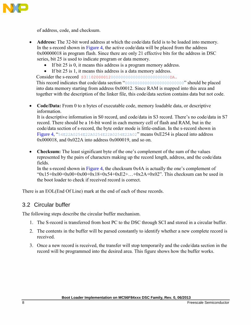
char get_byte(char **ptr)
This function reads out the current and next data that the pointer ptr points at and increases ptr by 2.
The two ASCII data are first transformed into corresponding integers and then concatenated together
to be the returned value. The following figure shows how it works.
Boot Loader Implementation on MC56F84xxx DSC Family, Rev. 0, 06/2013
Freescale Semiconductor 11
S 3 1 5 0 0 0 0 0 0 1 8 5 4 E 2 2
Data_in
ptrBefore get_byte(ptr) is invoked
S 3 1 5 0 0 0 0 0 0 1 8 5 4 E 2 2
Data_in
ptrAfter get_char(ptr) is invoked.
A byte with value of 0x15 is returned
Figure 7. get_byte() function
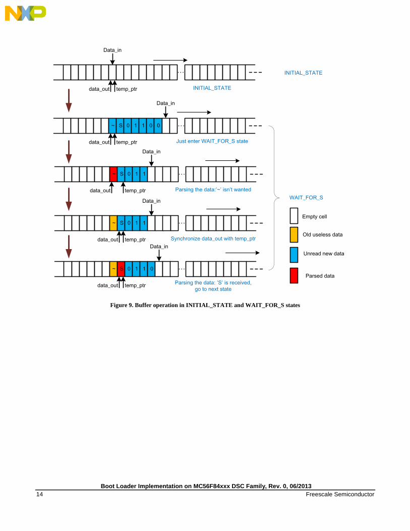
3.3 Boot loader state machine realization
The boot loader state machine performs the shadowed part of Figure 3. There are four states:
INITIAL_STATE, WAIT_FOR_S, WAIT_FOR_0, and WAIT_FOR_EOL. XON/XOFF protocol is
used so that hyperterminal on the PC can be used to transfer the s-record file.
A temporary pointer called temp_ptr is used to parse the received data in the circular buffer. Three
pointers data_in, data_out, and temp_ptr point to the same place in the buffer when the state machine
just starts, and the buffer is empty. The following figure shows the implementation of boot loader state
machine through the flowchart.

Boot Loader Implementation on MC56F84xxx DSC Family, Rev. 0, 06/2013
12 Freescale Semiconductor
INITIAL_STATE
WAIT_FOR_S
WAIT_FOR_0
WAIT_FOR_EOL
New data into the
buffer
Error occurs
Error occurs
Error occurs
‘S’ is received
‘0’ is next to ‘S’
The data next to ‘S’ in
the buffer isn’t ‘0’
No ‘S’ is received by
parsing the buffer
Parse the buffer for ‘\r’
Send XON flag
Send XOFF flag if current state is XON.
Program the record into flash
Send XON flag if the
buffer has no new data
‘\r’ is found in the
buffer
Figure 8. State machine flowchart
The s-record file of DSC always starts with S0 record, followed by several S3 records, and ends with S7
record. So, if this file is transferred by host through SCI, the same sequence is followed. As indicated in
Figure 8, the state machine can be explained as follows.
1. In the INITIAL_STATE, XON flag is sent to the host telling it to start transferring the s-record file.
2. If the buffer stays empty after a specified period of time (~10 seconds), the program will jump to the
user application and the boot loader is bypassed.
3. If the buffer is updated within the specified time, WAIT_FOR_S state is entered and the timeout
counter is stopped. The buffer has new data input if the pointer data_in does not equal temp_ptr.
4. In the state WAIT_FOR_S, the buffer is parsed by invoking get_char (&temp_ptr). If ‘S’ is found in
the buffer, it will enter WAIT_FOR_0 state. If not, it will stay in WAIT_FOR_S state and buffer is
parsed to get ‘S’. It must be noted that the host keeps sending data to the DSC in this state since the
communication state is XON.
If the baud rate is low, the buffer is parsed only if there are new data in it and so, there’s no
problem.
If the baud rate is too high, there could be a problem since the new data may overlap the old ones

Boot Loader Implementation on MC56F84xxx DSC Family, Rev. 0, 06/2013
Freescale Semiconductor 13
before the old ones are parsed by invoking get_char(&temp_ptr). In this state, the pointer
data_out is always synchronized with temp_ptr, so that data_out will always point to the place
where ‘S’ resides.
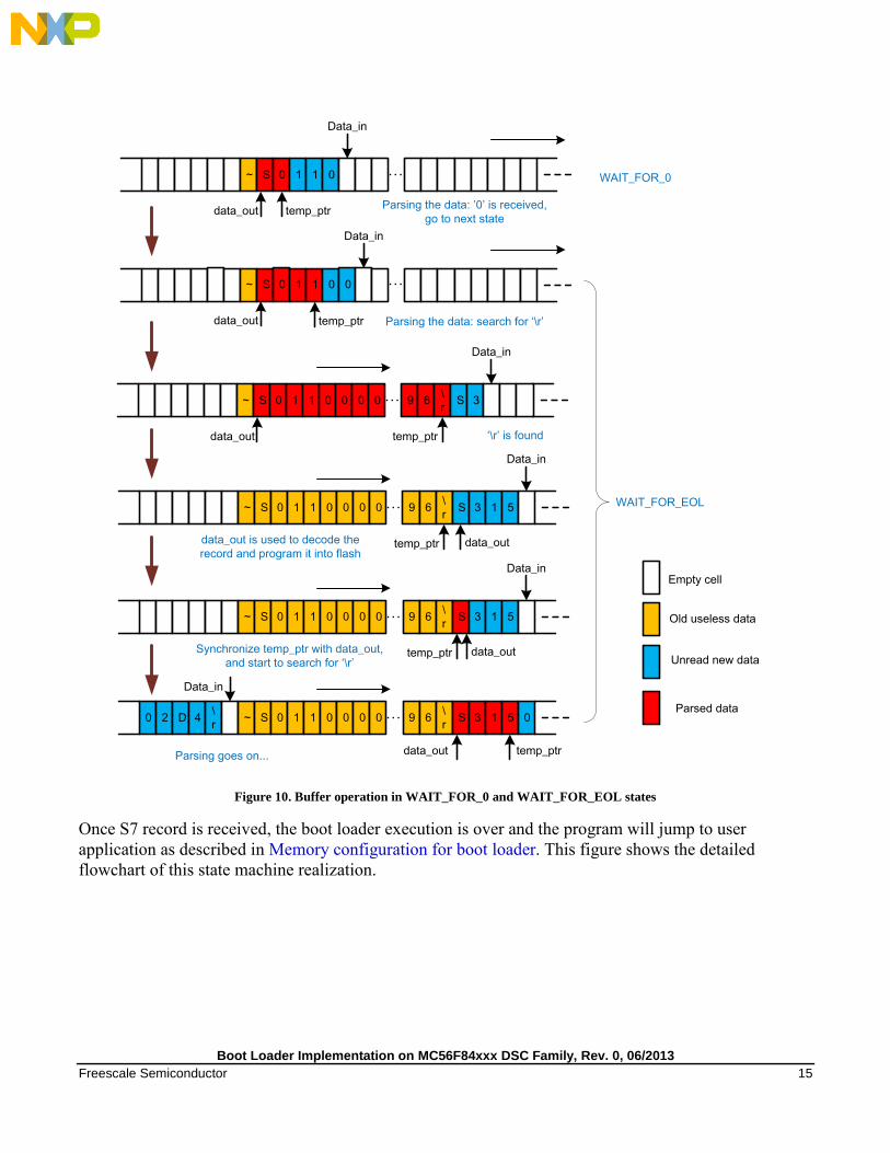
5. In the state WAIT_FOR_0, if ‘0’ is found next to ‘S’ in the buffer, it will enter WAIT_FOR_EOL
state, else it will return back to WAIT_FOR_S state.
6. The code section in a record is programmed into flash memory in the WAIT_FOR_EOL state.
a) First, the buffer continues to be parsed by invoking get_char(&temp_ptr) until the EOL flag ‘\r’
is found in the buffer.
b) Once ‘\r’ is found, XOFF flag is sent to the host telling it to pause the data transfer, and the
code section in the record indicated by the EOL flag just found is programmed into the flash
memory. Since data_out points at the place where ‘S’ of this record resides, it can be used to
analyze the record to get the code section.
c) After current record is programmed into flash, data_out will point to the place where ‘S’ of next
record resides naturally, and temp_ptr is synchronized with data_out for the search of next
EOL, namely ‘\r’ character.
Figure 9 and Figure 10 show the circular buffer status of every boot loader state.
Boot Loader Implementation on MC56F84xxx DSC Family, Rev. 0, 06/2013
14 Freescale Semiconductor
Data_in
temp_ptrdata_out INITIAL_STATE
~ S 0 1 1 0 0
Data_in
temp_ptrdata_out Just enter WAIT_FOR_S state
~ S 0 1 1
Data_in
temp_ptrdata_out Parsing the data:’~’ isn’t wanted
~ S 0 1 1
Data_in
temp_ptrdata_out Synchronize data_out with temp_ptr
~ S 0 1 1 0
Data_in
temp_ptrdata_outParsing the data: ’S’ is received,
go to next state
INITIAL_STATE
WAIT_FOR_S
Empty cell
Old useless data
Unread new data
Parsed data
Figure 9. Buffer operation in INITIAL_STATE and WAIT_FOR_S states
Boot Loader Implementation on MC56F84xxx DSC Family, Rev. 0, 06/2013
Freescale Semiconductor 15
~ S 0 1 1 0
Data_in
temp_ptrdata_outParsing the data: ’0’ is received,
go to next state
~ S 0 1 1 0 0
Data_in
temp_ptrdata_out Parsing the data: search for ‘\r’
~ S 0 1 1 0 0 0 0 9 6\
rS 3
Data_in
temp_ptrdata_out ‘\r’ is found
~ S 0 1 1 0 0 0 0 9 6\
rS 3 1 5
Data_in
temp_ptr data_outdata_out is used to decode the
record and program it into flash
~ S 0 1 1 0 0 0 0 9 6\
rS 3 1 5
Data_in
temp_ptr data_outSynchronize temp_ptr with data_out,
and start to search for ‘\r’
0 2 D 4\
r~ S 0 1 1 0 0 0 0 9 6
\
rS 3 1 5 0
Data_in
temp_ptrdata_outParsing goes on...
Empty cell
Old useless data
Unread new data
Parsed data
WAIT_FOR_0
WAIT_FOR_EOL
Figure 10. Buffer operation in WAIT_FOR_0 and WAIT_FOR_EOL states
Once S7 record is received, the boot loader execution is over and the program will jump to user
application as described in Memory configuration for boot loader. This figure shows the detailed
flowchart of this state machine realization.

Boot Loader Implementation on MC56F84xxx DSC Family, Rev. 0, 06/2013
16 Freescale Semiconductor
state == INITIAL_STATE?
Clear bootloader status.
Send ‘XON’ flag through SCI informing PC to transfer data
state = WAIT_FOR_S
data_in != temp_ptr?
Stop timer
State == WAIT_FOR_S?
temp_ptr = data_out.
Make temp_ptr point at the very first new data
in the buffer
get_char(&temp_ptr) == ‘S’?
state = WAIT_FOR_0
get_char(&data_out).
Synchronize data_out with temp_ptr.
State == WAIT_FOR_0?
get_char(&temp_ptr) == ‘0’?
state = WAIT_FOR_EOL
get_char(&data_out).
Synchronize data_out with temp_ptr.
state = WAIT_FOR_S
State == WAIT_FOR_EOL?
get_char(&temp_ptr) == ‘\r’?
PC’s sending data?
Send ‘XOFF’ flag
temp_ptr = data_out.
Make temp_ptr point at the very first new data
in the buffer
Decode the record and
program the code into flash
State = INITIAL_STATE
Y
Y,new data in the buffer
N
Y
Y
N
PC’s NOT sending data?
Any error occurs?
Bootloader is over?
N
Y
N
Y
N
Y
N
N
Y
Y
Y
N
N
state = INITIAL_STATE,
Display error code on PC.
Time’s up?
Jump to user’s
application
N
Y
Y
N
Send ‘XON’ flagN Y
N
Figure 11. Detailed flowchart of boot loader state machine
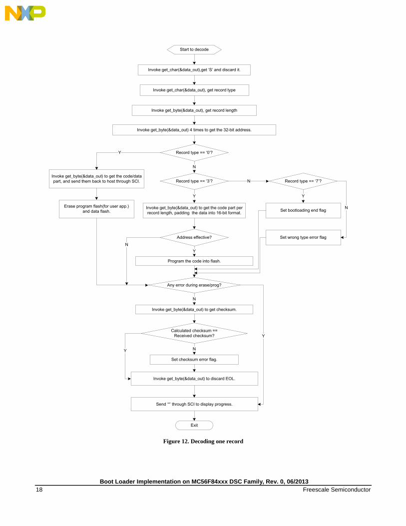
3.4 Decoding of s-record
As mentioned in Boot loader state machine realization, the record will be decoded and programmed into
flash once the corresponding EOL is found in the buffer. The following section describes how it works.
The pointer data_out always points at the first character of the record once the decoding starts, (as
shown in Figure 10). The function srec_decode() is used to decode the record together with the pointer
data_out. Following is a list of steps performed for decoding one s-record. Figure 12 shows the
flowchart of these steps.
1. The pointer data_out points at the beginning of the record which is ‘S’ when the decoding starts.
2. Invoke get_char(&data_out) twice to get the record type, and data_out points at the first character of

Boot Loader Implementation on MC56F84xxx DSC Family, Rev. 0, 06/2013
Freescale Semiconductor 17
the address section.
3. Invoke get_byte(&data_out) four times to fetch the address. Checksum is calculated every time
get_byte() is invoked.
4. Deal with code/data section of the record according to the type.
For type 0 (S0), fetch the code/data section by invoking get_byte(&data_out) and send them
back to the host, so the host will receive a string “PROGRAM&DATA”.
For type 3 (S3), fetch the code/data section and program them into the flash memory
according to the address.
For type 7(S7), the code/data section is fetched but ignored.
5. Once the code/data section is processed, get_byte(&data_out) is invoked to get checksum and it is
compared with the calculated one. The pointer data_out is made to point at the beginning of next
record by invoking get_byte(&data_out) again.
6. Once the record of type 7 is processed, boot loader execution is over.
3.5 Erase/program flash memory
The flash memory is configured, erased, and programmed by simply entering proper values such as
command code and data to the FTFL_FCCOBn registers. The execution of this command is started by
clearing bit 7 of the FTFL_FSTAT register. For detailed description of manipulating the flash memory
of MC56F84xxx, see MC56F847XXRM: MC56F847xx Reference Manual, available on freescale.com.
The following three commands are essential during the boot loader execution (since all the commands
are not used).
Erase Flash Block command
Erase Flash Sector command
Program Longword command
The flash address used in these commands is not the actual address that appears in the program memory
map or data memory map, as indicated in Figure 1.
The address used in the flash command is byte address, while the address mapped into program/data
memory is word address. For program flash, the command address starts from 0x000000 and for data
flash, it starts from 0x800000.
For instance, a 16-bit data of value 0x1122 is stored in the address of 0x0001 which is in the program
memory map. From the point of using flash commands, an 8-bit data of value 0x22 is stored in the byte
address of 0x0002 and an 8-bit value of 0x11 is stored in the byte address of 0x0003. The same rule
applies to the data flash. Figure 13 shows the relationship between word address and byte address.
Boot Loader Implementation on MC56F84xxx DSC Family, Rev. 0, 06/2013
18 Freescale Semiconductor
Start to decode
Invoke get_char(&data_out),get ‘S’ and discard it.
Invoke get_char(&data_out), get record type
Invoke get_byte(&data_out), get record length
Invoke get_byte(&data_out) 4 times to get the 32-bit address.
Record type == ‘0’?
Invoke get_byte(&data_out) to get the code/data
part, and send them back to host through SCI.
Erase program flash(for user app.)
and data flash.
Any error during erase/prog?
Invoke get_byte(&data_out) to get checksum.
Calculated checksum ==
Received checksum?
Set checksum error flag.
Invoke get_byte(&data_out) to discard EOL.
Send ‘*’ through SCI to display progress.
Invoke get_byte(&data_out) to get the code part per
record length, padding the data into 16-bit format.
Record type == ‘3’?
Address effective?
Program the code into flash.
Record type == ‘7’?
Set bootloading end flag
Set wrong type error flag
Exit
Y
N
Y
N
Y
Y
Y
N
NY
N
N
Figure 12. Decoding one record

Boot Loader Implementation on MC56F84xxx DSC Family, Rev. 0, 06/2013
Freescale Semiconductor 19
...
0x1122
...
...
Address
In program memory map
0x0000
0x0001
0x0002
0x0003
Program Flash
...
...
0x22
0x11
...
...
...
...
Address for flash
commands
Program Flash
0x0000
0x0001
0x0002
0x0003
0x0004
0x0005
0x0006
0x0007
...
0x1122
...
...
Address
In program memory map
0x68000
0x68001
0x68002
0x68003
Data Flash
...
...
0x22
0x11
...
...
...
...
Address for flash
commands
Data Flash
0x800000
0x800001
0x800002
0x800003
0x800004
0x800005
0x800006
0x800007
Figure 13. Relationship between word address and byte address
It must be noted that the 32-bit address in the record uses bit 25 to indicate whether the address is in
program memory or in data memory. A value of 1 indicates data memory.
Once an ‘S3’ record is detected, the code/data section will be fetched and entered into a 16-bit array in
the srec_decode() function. This 16-bit array, the 32-bit address decoded from the record, and the length
of the record are passed down to the flash programming function hfm_command(). This function first
analyzes the 32-bit address to find out whether it is a program memory or data memory address by
checking its bit 25, and then changes it into byte address used by flash commands. The 16-bit array with
code inside is transformed into 8-bit array just by using a ‘Word8 *’ type pointer. The compiler will deal
with the relationship in Figure 13 automatically.
The program flash and data flash will be erased if the record under processing is type 0. Program
longword command is used while processing record of type 3. Program longword means programming
four bytes data into the flash starting with the command address, and the command address must be
longword-aligned, which means the last two bits of this address must be 0b00. There are circumstances
where the command address is not longword-aligned. Figure 14 shows how to deal with it.

Boot Loader Implementation on MC56F84xxx DSC Family, Rev. 0, 06/2013
20 Freescale Semiconductor
0x13 0x15 0xA4 0x45 0x15 0xE4 0x90 0x03
0x0082
0x13 0x15 0xA4 0x45 0x15 0xE4 0x90 0x03
0x0080
0xFF 0xFF
Addr (for cmd):
Addr (for cmd): 0x0082
0xFF 0xFF
Make it longword aligned and
the length to be a multiple of 4.
Figure 14. Dealing with the byte array without having longword-aligned address
As shown in Figure 14, the start address is 0x0082 which is not longword-aligned. Add 2-byte data of
0xFF in front of this array so that the start address is 0x0080, which is longword-aligned. Programming
0xFF into a cell actually has no meaning because ‘0’ can’t be changed into ‘1’ through Flash Program
command. 2-byte data of 0xFF are also added at the end of this array in order to make the length of this
array to be a multiple of four bytes, because Program Longword command always programs four bytes
at a time.
4 Software introduction
The code for this boot loader is developed in CodeWarrior v10.3 (build ID: 121211) based on PE. This
section will discuss some key points regarding development of this code in CW v10.3.
4.1 Linker file
The default linker file generated by PE doesn’t apply to this specific application. It must be modified
according to Figure 2. The MEMORY part is shown as the following code.
MEMORY {
.pIntvectorBoot (RWX): ORIGIN = 0x00000000, LENGTH = 0x000000F0 # Reset and cop vectors
.pFlashConfig (RWX): ORIGIN = 0x00000200, LENGTH = 0x00000008 # Reserved for Flash IFR value
.ppFlash (RWX): ORIGIN = 0x00000208, LENGTH = 0x0001F1F5 # Primary flash for user code
.DelayT (RWX): ORIGIN = 0x0001F3FD, LENGTH = 0x00000003 # Bootloading delay time & user code start position
.pFlash (RWX): ORIGIN = 0x0001F400, LENGTH = 0x00000C00 # Primary flash for boot loader, 3Kwords
.xRAM_bss (RW) : ORIGIN = 0x00000000, LENGTH = 0x00000800 # 2Kwords for bss
.xRAM_data (RWX): ORIGIN = 0x00000800, LENGTH = 0x00000200 # 0.5Kwords for global variables
.xRAM (RW) : ORIGIN = 0x00000A00, LENGTH = 0x00001600 # 5.5Kwords for heaps and stacks
.pRAM_code (RWX): ORIGIN = 0x00062000, LENGTH = 0x00002000 # 8Kwords for code
.xRAM_code (RW) : ORIGIN = 0x00002000, LENGTH = 0x00002000 # mirror of .pRAM_code
}

Boot Loader Implementation on MC56F84xxx DSC Family, Rev. 0, 06/2013
Freescale Semiconductor 21
It is recommended that the flash erase/program function hfm_command() (see Erase/program flash
memory) is executed in program RAM. So, this function must be stored in flash memory but run in
RAM, which is realized in the following code description of SECTIONS part.
.ApplicationCode :
{
_pFlash_code_start = .;
# Note: The function _EntryPoint should be placed at the beginning of the code
OBJECT (F_EntryPoint, Cpu_c.obj)
# Remaining .text sections
* (rtlib.text)
* (startup.text)
* (fp_engine.text)
* (user.text)
* (.text)
# save address for the data starting in pROM
Fpflash_mirror = .;
Fpflash_index = .;
} > .pFlash
.prog_in_p_flash_ROM : AT(Fpflash_mirror)
{
Fpram_start = .;
_pram_start = .;
* (interrupt_vectors.text)
* (pram_code.text)
# save data end and calculate data block size
Fpram_end = .;
Fpram_size = Fpram_end - Fpram_start;
_pram_size = Fpram_size;
Fpflash_mirror2 = Fpflash_mirror + Fpram_size;
Fpflash_index = Fpflash_mirror + Fpram_size;
} > .pRAM_code
Global constants are defined in the linker file to identify the start address and the size of this function in
flash memory and RAM.
F_pflash_code_start = Fpflash_mirror; # start address in Flash
F_dram_code_start = _pram_start - 0x60000; # start address in RAM (the address mapped into data memory)
F_dram_code_size = _pram_size; # size
The function code is copied from flash memory to RAM using the mem_copy() function, the moment it
enters main() function. The default memory copy routine in “56F83x_init.asm” generated by PE is not
used, so two constants must be set to 0 in the linker file as shown in the following code.
F_xROM_to_xRAM = 0x0000;
F_pROM_to_xRAM = 0x0000;

Boot Loader Implementation on MC56F84xxx DSC Family, Rev. 0, 06/2013
22 Freescale Semiconductor
The mem_copy function is defined in the following code.
asm void mem_copy(long p_start,long x_start,unsigned int cnt)
{
move.l a10,r2
move.l b10,r3
do y0,>>end_prom2xram // copy for 'cnt' times
move.w p:(r2)+,x0 // fetch value at p-address
nop
nop
nop
move.w x0,x:(r3)+ // stash value at x-address
end_prom2xram:
nop
rts
}
The default configuration generated by PE is small data model, which means only 16-bit pointer can be
used and it speeds up the execution of the boot loader to a certain extent. As Figure 2 shows, the code
starts at 0x1F400 which is a 17-bit address; so, to avoid compile error, the functions
F_pflash_code_start and F_dram_code_start are divided into two parts as shown in the following code
lines.
F_pflash_code_start_h = (F_pflash_code_start/65536)&0xffff;
F_pflash_code_start_l = F_pflash_code_start &0xffff;
F_dram_code_start_h = (F_dram_code_start/65536) &0xffff;
F_dram_code_start_l = F_dram_code_start &0xffff;
The function mem_copy is invoked using the following code.
mem_copy(((Word32)(&_pflash_code_start_h)<<16) + (Word32)(&_pflash_code_start_l),\
((Word32)(&_dram_code_start_h)<<16) + (Word32)(&_dram_code_start_l),(UWord16)&_dram_code_size);
The .data sections are processed in the similar manner. Once the linker file is generated by PE, prohibit
PE from generating linker file every time the project is compiled by selecting ‘no’ in the “Generate
linker file” option. The following figure shows where to change this setting.

Boot Loader Implementation on MC56F84xxx DSC Family, Rev. 0, 06/2013
Freescale Semiconductor 23
Figure 15. PE Option to prohibit PE from generating linker file
For more information about code implementation, see the source code project AN4759SW, attached
with this application note.
4.2 The do's and don'ts of implementing the boot loader
For those who are not familiar with CodeWarrior v10.3 and MC56F84xxx DSC series, the following
key points need to be mentioned.
The watchdog is enabled by default.
The start address of the boot loader must be right on the border of a sector which is 1 K words in
program flash. This is because the flash is erased in the unit of sector which means that if you want
to erase some cells in the flash memory, you'll have to erase the whole 1 K words memory where the
cells belong to.
When SCI is used for communication, and Init_SCI bean is used in PE, remember to disable its
DMA function, else there will be receiving error unless DMA function is indeed used.
“Clean project” must be executed after linker file is changed, else it won’t take effect.
The circular buffer used in this application is realized by modulo addressing function of the core,
and requires the start address to be an even value.
SCI interrupt in this application is fast interrupt which means the program will go to the interrupt
service routine directly without jumping to the vector table first. So if fast interrupt is not used, the
start address of the interrupt vector table should be altered to avoid conflict between the user

Boot Loader Implementation on MC56F84xxx DSC Family, Rev. 0, 06/2013
24 Freescale Semiconductor
application and the boot loader.
5 User application requirements
If the user application is based on PE, the following two issues must be considered, so that the
application can be downloaded properly through the boot loader developed above, and the boot loader
can still function well together with user application:
The linker file generated by PE should be prohibited to update automatically. Figure 15 shows the
setting. The memory for code can’t go beyond 0x1F3FF in program flash as indicated in Figure 2.
The start address of the user application and the delay time must be entered in the address range
0x1F3FD-0x1F3FF.
MEMORY {
……
.p_Code (RWX) : ORIGIN = 0x00000208, LENGTH = 0x000F000
……
.xBootCfg (RWX): ORIGIN = 0x1F3FD, LENGTH = 3
}
SECTIONS{
.ApplicationConfiguration:
{
# Store the application entry point
WRITEW(F_EntryPoint); # write 4 bytes
# Boot loader start delay in seconds
WRITEH(12); # write 2 bytes
} > .xBootCfg
}
Modification should be made to “Vector.c” generated by PE. The first two instructions in _vect()
function must be changed as shown in the following code, so that the program will first jump to the
boot loader once the chip is reset.

Boot Loader Implementation on MC56F84xxx DSC Family, Rev. 0, 06/2013
Freescale Semiconductor 25
#define boot_start 0x1f400
#pragma define_section interrupt_vectors "interrupt_vectors.text" RX
#pragma section interrupt_vectors begin
volatile asm void _vect(void) {
JMP boot_start /* Interrupt no. 0 (Used) - ivINT_HW_RESET */
JMP boot_start /* Interrupt no. 1 (Used) - ivINT_COP_RESET */
……
……
}
#pragma section interrupt_vectors end
Vector.c should remain this way once it is changed as above. The following figure shows how to freeze
the code generation function by PE.
Figure 16. Option to freeze the code generation function by PE
1. S-record won’t be generated by default; it should be enabled as shown in Figure 17. The option Sort
by Address must be selected and the max s-record length shouldn’t exceed 255. S-record EOL
character should be DOS(\\r\\n).
2. As for how to use hyperterminal together with this boot loader to realize the boot loader function,
see AN4275: Serial Boot loader for 56F82xx, available on freescale.com.

Boot Loader Implementation on MC56F84xxx DSC Family, Rev. 0, 06/2013
26 Freescale Semiconductor
Figure 17. Configuration of generating s-record
6 Conclusion
This application note provides a method of realizing boot loader on 56F84xxx series. This document
also describes in detail, the working of the boot loader and its implementation using CodeWarrior v10.3
with Processor Expert. Both MC56F84xxx and MC56F827/3xx DSC series can take the sample code as
reference.
7 References
MC56F847XXRM: MC56F847xx Reference Manual, available on freescale.com
AN4689: EEPROM on MC56F84xxx DSC, available on freescale.com
DSP56800E and DSP56800EX Reference Manual, available on freescale.com
AN4275: Serial Boot loader for 56F82xx, available on freescale.com

Boot Loader Implementation on MC56F84xxx DSC Family, Rev. 0, 06/2013
Freescale Semiconductor 27
8 Revision history
Revision number Date Substantive changes
0 06/2013 Initial release

How to Reach Us Home Page: freescale.com Web Support: freescale.com/support
Information contained in this document is provided solely to enable system and software implementers to use Freescale products. There are no express or implied copyright licenses granted hereunder to design or fabricate any integrated circuits based on the information in this document. Freescale reserves the right to make changes without further notice to any products herein. Freescale makes no warranty, representation, or guarantee regarding the suitability of its products for any particular purpose, nor does Freescale assume any liability arising out of the application or use of any product or circuit, and specifically disclaims any and all liability, including without limitation consequential or incidental damages. “Typical” parameters that may be provided in Freescale data sheets and/or specifications can and do vary in different applications, and actual performance may vary over time. All operating parameters, including “typicals,” must be validated for each customer application by customer’s technical experts. Freescale does not convey any license under its patent rights nor the rights of others. Freescale sells products pursuant to standard terms and conditions of sale, which can be found at the following address: freescale.com/SalesTermsandConditions.
Freescale, the Freescale logo, CodeWarrior, and Processor Expert are trademarks of Freescale Semiconductor, Inc., Reg. U.S. Pat. & Tm. Off. All other product or service names are the property of their respective owners.
© 2013 Freescale Semiconductor, Inc.
Document Number: AN4759
Rev. 0, 06/2013
June 23, 2013