analog dialogue volume 45, number 3, 2011 · 3 power management design for ... circuits all seeing...
TRANSCRIPT

www.analog.com/analogdialogue
Volume 45, Number 3, 2011 A forum for the exchange of circuits, systems, and software for real-world signal processing
In This Issue 2 Editors’ Notes; New Product Introductions
3 Power Management Design for PLLs
7 Insight into digiPOT Specifications and Architecture Enhances AC Performance
11 Differential Interfaces Improve Performance in RF Transceiver Designs
16 How to Apply DC-to-DC Step-Up (Boost) Regulators Successfully
19 System Demonstration Platform Facilitates Quick Prototyping and Evaluation
22 Simple Ambient Light Sensor Circuit

2 ISSN 0161-3626 ©Analog Devices, Inc. 2011
Editors’ NotesIN THIS ISSUE
Power Management Design for PLLsPhase-locked loops are typically used to provide local oscillators in radio receivers and transmitters, for clock-signal distribution and noise reduction, and as the clock source for high-speed analog-to-digital and digital-to-analog converters. As PLL noise decreases, the impact of power supply noise increases—and can even limit noise performance in some cases. This article considers basic PLLs and the power-management requirements for each PLL building block. Page 3.
Insight into digiPOT Specifications and Architecture Enhances AC PerformanceDigital potentiometers provide a convenient way to adjust the output of sensors, power supplies, or other devices that require calibration. Digital setting avoids problems associated with mechanical potentiometers, such as physical size, mechanical wear out, wiper contamination, resistance drift, and sensitivity to environmental effects—and eliminates layout inflexibility resulting from the need for physical access. Page 7.
Differential Interfaces Improve Performance in RF Transceiver DesignsTraditional IF and RF transceivers use 50-Ω single-ended interfaces, with interconnected circuits all seeing matching input and output impedances. In modern transceiver designs, differential interfaces provide better performance, but their implementation requires designers to confront impedance matching, common-mode voltage matching, and difficult gain calculations. This article offers some assistance. Page 11.
How to Apply DC-to-DC Step-Up (Boost) Regulators SuccessfullyBattery-powered systems often stack cells in series to achieve higher voltages, but this is not always possible due to a lack of space. Switching converters use an inductor’s magnetic field to alternately store energy and release it to the load at a different voltage. With low losses they are a good choice for high efficiency. Boost, or step-up, converters—featured here—provide higher voltage. Page 16.
System Demonstration Platform Facilitates Quick Prototyping and EvaluationSystem design can be complex, but the ability to prototype and quickly demonstrate subsections of the solution can simplify the process and reduce the risks faced by designers. With the System Demonstration Platform (SDP), system designers can reuse central elements, allowing subsections of their designs to be evaluated and demonstrated prior to the final system implementation. Page 19.
Simple Ambient Light Sensor CircuitAmbient light is increasingly considered as a source for harvesting energy to power heartbeat monitors, bathroom fixtures, remote weather sensors, and other low-power devices. At the heart of an energy-harvesting system is the ability to measure ambient light accurately. This design idea describes a simple, cost-effective circuit that provides a voltage proportional to the intensity of ambient light. Page 22.
Dan Sheingold [[email protected]]
Scott Wayne [[email protected]]
PRODUCT INTRODUCTIONS: VOLUME 45, NUMBER 3Data sheets for all ADI products can be found by entering the part
number in the search box at www.analog.com.JulyAccelerometer, ±2-g, dual-axis, PWM output ........................ ADXL212Accelerometer, ±5-g, dual-axis, 175°C operation .................... ADXL206ADC, dual, 12-bit, 170-MSPS/210-MSPS/250-MSPS ................ AD9613ADC, dual, 14-bit, 170-MSPS/210-MSPS/250-MSPS ................ AD9643Codec, stereo audio, speaker/headphone amplifiers ................ ADAU1373Converter, dc-to-dc, 3-MHz, buck, 800-mA drive ................... ADP2147Converters, dc-to-dc, 6-MHz, buck, 500-mA drive ........................................................ ADP2126/ADP2127DAC, quad, 16-bit, voltage/current output ................................... AD5755Front End, analog, ADC, 6-channel LNA/PGA/AAF ................ AD8283Micro PMU, two 800-mA bucks, two 300-mA LDOs .............. ADP5033Modulator, quadrature, 1550-MHz to 2650-MHz ................ ADRF6703Multiplexer, 4:1, high-voltage, latch-up proof ......................... ADG5204Receiver, dual IF ........................................................................ AD6643Receiver, IF diversity ................................................................. AD6649Switch, digital crosspoint, 4.25-Gbps, 40 × 40 ........................ ADN4605Switch, high-side power, logic-level control ................................ ADP194Transmitter, HDMI, 12-bit, 165-MHz ................................. ADV7511W
AugustRegulator, dual, 3-A, 20-V, step-down ..................................... ADP2323Switch, dual SPDT, high-voltage, latch-up proof ...................... ADG5236Transceiver, CAN, isolated, bus-side dc-to-dc ........................ ADM3053Transceiver, CAN, isolated, bus-side LDO ............................. ADM3052
SeptemberAmplifier, driver, 1-W, 700-MHz to 1000-MHz ...................... ADL5605Amplifier, driver, 1-W, 1800-MHz to 2700-MHz .................... ADL5606Amplifier, instrumentation, dual, rail-to-rail ............................. AD8426Amplifier, operational, dual, RRIO, OVP ............................ ADA4096-2Amplifiers, operational, single/dual low-noise ... ADA4897-1/ADA4896-2Audio, Class-D speaker and capless headphone drivers ............. SSM2804Controllers, dc-to-dc, buck ..................................... ADP1878/ADP1879Converter, rms-to-dc ................................................................. AD8436DAC, quad, 12-bit, current output, HART connectivity .............. AD5737DAC, quad, 12-bit, voltage/current output ................................... AD5735DAS, 8-channel, 18-bit, simultaneous-sampling ADC ................ AD7609Detector, envelope and rms, dc to 6-GHz ................................. ADL5511Drivers, triple, differential, wideband video .................. AD8141/AD8142Micro PMU, two 1200-mA bucks, two 300-mA LDOs ............ ADP5034Mixer, balanced, 2300-MHz to 2900-MHz .............................. ADL5363Mixer, doubly balanced, 700-MHz to 2800-MHz .................... ADL5811Mixer, dual, doubly balanced, 700-MHz to 2800-MHz ............ ADL5812 Multiplexer, 4:1, differential, high-voltage, latch-up proof ........................................................................ ADG5209 Multiplexer, 8:1, high-voltage, latch-up proof ......................... ADG5208Receiver, HDMI, 3-GHz, dual-port, Xpressview™ .................. ADV7619Receiver, MIPI/DSI, HDMI transmitter .................................. ADV7533Regulators, voltage, dual, adjustable-output, 300-mA drive ............................................................ ADP223/ADP225Regulators, voltage, dual, fixed-output, 300-mA drive ............................................................ ADP222/ADP224Sensor, vibration, 3-axis, digital, FFT analysis ...................... ADIS16228Switches, triple/quad SPDT, high-voltage, latch-up proof ....................................................... ADG5233/ADG5234Synthesizer, PLL, fractional-N/integer-N ............................... ADF4150Transceivers, RS-485, 500-kbps/16-Mbps, 5-kV isolation ................................................. ADM2682E/ADM2687E VGAs, digitally controlled, 100-MHz to 4000-MHz ........................................ ADL5240/ADL5243
Analog Dialogue, www.analog.com/analogdialogue, the technical magazine of Analog Devices, discusses products, applications, technology, and techniques for analog, digital, and mixed-signal processing. Published continuously for 45 years—starting in 1967—it is available in two versions. Monthly editions offer technical articles; timely information including recent application notes, new-product briefs, webinars and tutorials, and published articles; and Potpourri, a universe of links to important and relevant information on the Analog Devices website, www.analog.com. Printable quarterly issues and ebook versions feature collections of monthly articles. For history buffs, the Analog Dialogue archive, www.analog.com/library/analogdialogue/archives.html, includes all regular editions, start ing with Volume 1, Number 1 (1967), and three special anniversary issues. To subscribe, please go to www.analog.com/library/analogdialogue/subscribe.html. Your comments are always welcome: Facebook: www.facebook.com/analogdialogue; Analog Diablog: analogdiablog.blogspot.com; Email: [email protected] or Dan Sheingold, Editor [[email protected]] or Scott Wayne, Publisher and Managing Editor [[email protected]].

Analog Dialogue Volume 45 Number 3 3
Power Management Design for PLLsBy Austin Harney and Grzegorz Wawrzola
AbstractThe phase-locked loop (PLL) is a fundamental building block of modern communication systems. PLLs are typically used to provide the local-oscillator (LO) function in a radio receiver or transmitter; they are also used for clock-signal distribution and noise reduction—and, increasingly, as the clock source for high-sampling-rate analog-to-digital or digital-to-analog conversion.
As the noise performance of PLLs is improving with each generation, the impact of power supply noise is becoming increasingly evident, and can even limit noise performance in some cases.
This ar t icle considers the basic PLL scheme shown in Figure 1 and examines the power-management requirements for each building block.
CHARGEPUMP
LOOPFILTER
VP3V TO 30V
0.5mA TO 5mALOW RIPPLE
AVDD/DVDD1.8V TO 5V
10mA TO 50mAMODERATE NOISE
VVCO3V TO 5V
25mA TO 300mAULTRALOW NOISE
VCO
N DIVIDER
PHASEDETECTOR
VOLTAGE-CONTROLLEDOSCILLATOR
Figure 1. A basic phase-locked loop showing the various power-management requirements.
In a PLL, the feedback control loop drives a voltage-controlled oscillator (VCO) to make the oscillator frequency (or phase) accurately track a multiple of an applied reference frequency. Many good references, for example, Best’s Phase-Locked Loops,1 explain the mathematical analysis of the PLL; and simulation tools, such as Analog Devices’ ADIsimPLL™, can be helpful in understanding the loop transfer functions and calculations. Let us now look at the PLL building blocks in turn.
The VCO and VCO PushingThe voltage-controlled oscillator converts the error voltage from the phase detector into an output frequency. Its “gain,” defined as KVCO, is usually specified in MHz/V. A voltage-controlled variable-capacitance diode (varactor) is often used to adjust frequency in VCOs. The gain of the VCO is usually large enough to provide adequate frequency coverage, but not so large as to degrade phase noise—since any varactor noise will be amplified by KVCO and contribute to output phase noise.
The advent of multiband integrated VCOs, such as that used in the ADF4350 frequency synthesizer with integrated VCO, obviates the trade-off between KVCO and frequency coverage, allowing the PLL designer to use an IC containing several moderate-gain VCOs, with intelligent band switching routines to select the appropriate band, depending on the programmed output frequency. This partitioning of the frequency band provides wide overall range and lower noise.
In addition to the desired translation from input voltage change to output frequency change (KVCO), power-supply variation can produce an unwanted component of output frequency change.
The sensitivity of the VCO to power-supply variation is defined as the VCO pushing (Kpushing), usually a fraction of the wanted KVCO. For example, Kpushing is usually 5% to 20% of KVCO. Thus, for high-gain VCOs, the pushing effect becomes larger, and the noise contribution from the VCO supply source becomes more critical.
VCO pushing is measured by applying a dc tuning voltage to the VTUNE pin, varying the power supply voltage, and measuring the frequency change. The pushing figure is the ratio of frequency change to voltage change, as shown in Table 1, using the ADF4350 PLL.
Table 1. ADF4350 VCO Pushing Measurements
VCO Band (MHz)
Vtune (V)
f1 (MHz) at VVCO = 3 V
f2 (MHz) at VVCO = 3.3 V
Kpushing = Δf/ΔV
(MHz/V)
2200 2.5 2233.446 2233.061 1.28
3300 2.5 3331.112 3331.799 2.3
4400 2.5 4462.577 4464.242 5.55
Another method, mentioned in Reference 2, is to dc-couple a low-frequency square wave into the supply, while observing the frequency-shift-keyed (FSK) modulation peaks on either side of the VCO spectrum (Figure 2). The frequency deviation between the peaks divided by the amplitude of the square wave yields the VCO pushing number. This can be a more accurate measure than the static dc test, as it removes any thermal effects associated with a change in dc input voltage. Figure 2 shows a spectrum analyzer plot of the ADF4350 VCO output at 3.3 GHz with a 10 kHz, 0.6 V p-p square wave applied to the nominal 3.3-V supply. The resulting deviation is 3326.51 MHz – 3324.89 MHz = 1.62 MHz, for a pushing number of 1.62 MHz/0.6 V or 2.7 MHz/V. This compares to the static measure of 2.3 MHz/V given in Table 1.
Figure 2. A spectrum-analyzer plot of ADF4350 VCO response to supply modulation by a 10-kHz, 0.6-V p-p square wave.
In a PLL system, higher VCO pushing means greater multiplication of VCO power-supply noise. A low-noise power supply is required to minimize the impact on VCO phase noise.
Reference 3 and Reference 4 provide good examples of how different low-dropout regulators (LDOs) can affect PLL phase-noise. For example, a comparison was made between the ADP3334 and ADP150 LDOs in powering an ADF4350. The integrated rms noise of the ADP3334 regulator is 27 µV (over four decades,

4 Analog Dialogue Volume 45 Number 3
from 10 Hz to 100 kHz). This compares to 9 µV for the ADP150, the LDO used on the ADF4350 evaluation board. The difference in measured PLL phase-noise spectral density can be seen in Figure 3. The measurement was taken with a 4.4-GHz VCO frequency, where the VCO pushing was maximum (Table 1), so this is a worst-case result. The ADP150 regulator noise was low enough so that its contribution did not measurably add to the VCO noise, as was confirmed by repeating the measurement with two (presumably “noiseless”) AA batteries.
–60
–70
–80
–90
–100
–110
–1201k 10k 100k 1M
PHA
SE N
OIS
E (d
Bc/
Hz)
OFFSET FROM 4.4GHz CARRIER (Hz)
SUPPLY 2 × ADP3334AA BATTERY (2 × 1.5V)SUPPLY 2 × ADP150
Figure 3. ADF4350 phase noise comparison at 4.4 GHz when powered with pairs of ADP3334 and ADP150 LDOs—and AA batteries.
Figure 3 emphasizes the importance of a low-noise power source for the ADF4350, but how do you specify the noise requirement of the power supply or LDO?
In a manner similar to VCO noise, the phase noise contribution of the LDO can be modeled as an additive component, ΦLDO(t), as shown in Figure 4. Reusing the VCO excess phase expression yields:
or, in the frequency domain
where vLDO( f ) is the voltage noise spectral density of the LDO.
The single-sideband power spectral density SΦ( f ) in a 1-Hz bandwidth is given by
Expressing this in dB, the formula for calculating the phase noise contribution due to the power supply noise is:
(1)
where L(LDO) is the noise contribution from the regulator to the VCO phase noise (in dBc/Hz), at an offset f; Kpushing is the VCO pushing figure in Hz/V; and vLDO( f ) is the noise spectral density at a given frequency offset in V/√Hz.
PHASEDETECTOR
LOW-PASSFILTER
÷NCOUNTER
VCO ΦOUT
ΦIN
ΦLDO
Figure 4. Small-signal additive VCO supply noise model.
In a free-running VCO, the total noise is the root-sum-square (rss) of LLDO and the VCO noise. Thus, expressed in dB:
For example, consider a VCO with a pushing number of 10 MHz/V and a measured phase noise of –116 dBc/Hz at 100 kHz offset: what is the required noise spectral density of the power supply so as to not degrade the VCO noise performance at 100 kHz? The supply noise and VCO noise add as the root-sum-square, so the supply noise should be at least 6 dB less than the VCO noise to minimize its contribution. Thus, LLDO should be less than –122 dBc/Hz. Using Equation 1,
solving for vLDO( f ),
vLDO( f ) = 11.2 nV/√Hz at 100-kHz offsetThe LDO noise spectral density at a given offset can usually be read from the LDO data sheet’s typical performance curves.
When the VCO is connected in a negative-feedback PLL, the LDO noise, LLDO, is high-pass filtered by the PLL loop filter, in a similar manner to VCO noise. Thus, the above formula only applies to frequency offsets greater than the PLL loop bandwidth. Within the PLL’s loop bandwidth, the PLL can successfully track and filter the LDO noise, reducing its contribution.
LDO FilteringTo improve LDO noise, there are typically two choices: use an LDO with less noise or post-filter the LDO’s output. The filtering option can be a good choice when the noise requirements without a filter are beyond the capability of affordable LDOs. A simple LC π-filter is often sufficient to reduce out-of-band LDO noise by 20 dB (Figure 5).
Figure 5. LC π-filter to attenuate LDO noise.
Care is needed in the choice of components. A typical inductor will be in the microhenry range—with a ferrite core—so it is necessary to consider its saturation current (ISAT), specified in inductor data sheets as the dc current level at which the inductance drops by 10%. The current drawn by the VCO should be less than ISAT. Effective series resistance (ESR) is also a concern, as this will cause an IR drop across the filter. For a microwave VCO drawing 300-mA dc, an inductor with ESR less than 0.33 Ω would be needed to yield an IR drop of less than 100 mV. A low, but nonzero, ESR is also desirable to damp the filter response and improve LDO stability. It can be practical to choose a capacitor with very low parasitic
Analog Dialogue Volume 45 Number 3 5
ESR and add a dedicated series resistor for this purpose. This can all be simulated easily in SPICE using a downloadable component evaluator such as NI Multisim™.
Charge Pump and FilterThe charge pump converts the phase detector error voltage into current pulses, which are integrated and smoothed by the PLL loop filter. The charge pump can typically operate at up to 0.5 V below its supply voltage (VP). For example, if the maximum charge pump supply is 5.5 V, the charge pump could only operate at an output voltage up to 5 V. If the VCO requires higher tuning voltages, an active filter is typically required. Useful information and a reference design of an actual PLL can be found in Circuit Note CN-0174,5 and ways of dealing with high-voltage are discussed in “Designing High-Performance Phase-Locked Loops with High-Voltage VCOs,”6 which appeared in Analog Dialogue Volume 43, Number 4 (2009). The alternative to an active filter is to use a PLL with a charge pump designed for higher voltage, such as the ADF4150HV. The ADF4150HV can operate with charge-pump voltages as high as 30 V, thus avoiding the need for active filters in many cases.
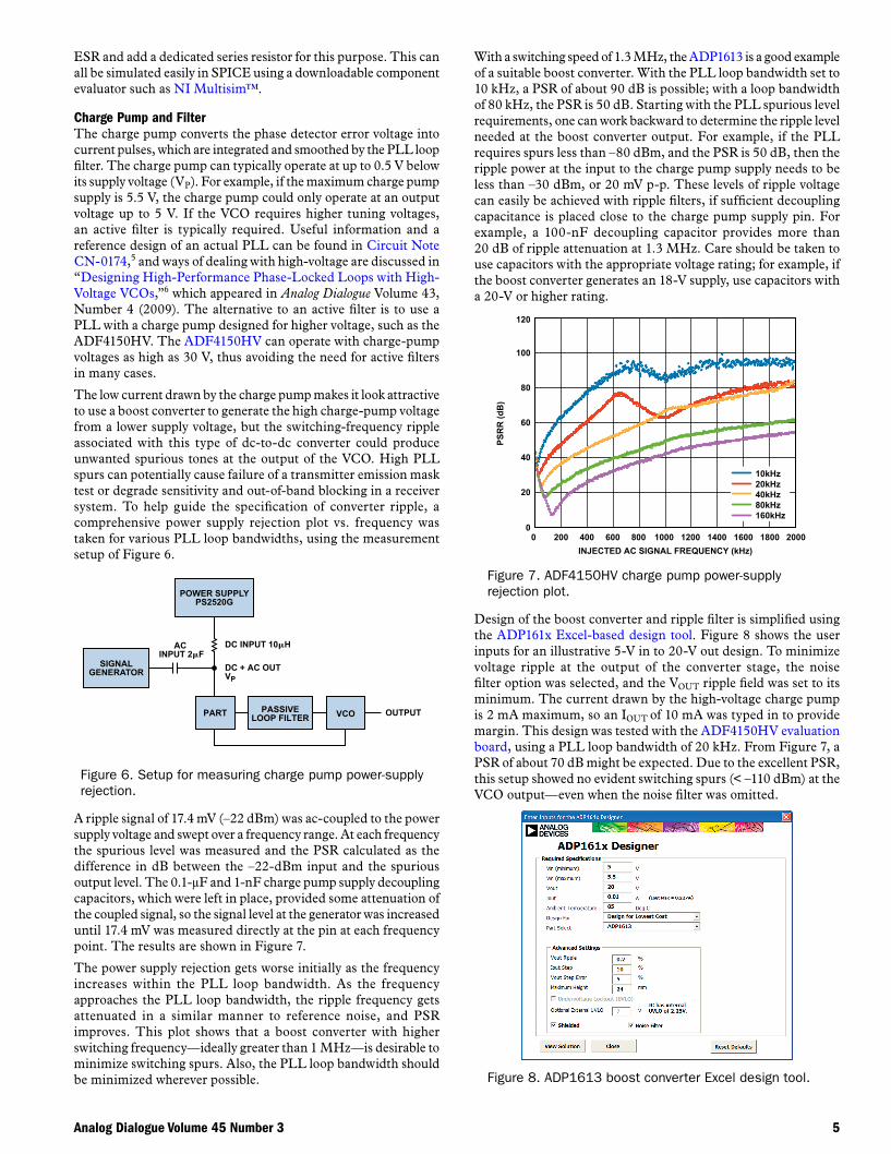
The low current drawn by the charge pump makes it look attractive to use a boost converter to generate the high charge-pump voltage from a lower supply voltage, but the switching-frequency ripple associated with this type of dc-to-dc converter could produce unwanted spurious tones at the output of the VCO. High PLL spurs can potentially cause failure of a transmitter emission mask test or degrade sensitivity and out-of-band blocking in a receiver system. To help guide the specification of converter ripple, a comprehensive power supply rejection plot vs. frequency was taken for various PLL loop bandwidths, using the measurement setup of Figure 6.
POWER SUPPLYPS2520G
SIGNALGENERATOR
AC INPUT 2�F
DC INPUT 10�H
DC + AC OUTVP
PART VCOPASSIVELOOP FILTER OUTPUT
Figure 6. Setup for measuring charge pump power-supply rejection.
A ripple signal of 17.4 mV (–22 dBm) was ac-coupled to the power supply voltage and swept over a frequency range. At each frequency the spurious level was measured and the PSR calculated as the difference in dB between the –22-dBm input and the spurious output level. The 0.1-μF and 1-nF charge pump supply decoupling capacitors, which were left in place, provided some attenuation of the coupled signal, so the signal level at the generator was increased until 17.4 mV was measured directly at the pin at each frequency point. The results are shown in Figure 7.
The power supply rejection gets worse initially as the frequency increases within the PLL loop bandwidth. As the frequency approaches the PLL loop bandwidth, the ripple frequency gets attenuated in a similar manner to reference noise, and PSR improves. This plot shows that a boost converter with higher switching frequency—ideally greater than 1 MHz—is desirable to minimize switching spurs. Also, the PLL loop bandwidth should be minimized wherever possible.
With a switching speed of 1.3 MHz, the ADP1613 is a good example of a suitable boost converter. With the PLL loop bandwidth set to 10 kHz, a PSR of about 90 dB is possible; with a loop bandwidth of 80 kHz, the PSR is 50 dB. Starting with the PLL spurious level requirements, one can work backward to determine the ripple level needed at the boost converter output. For example, if the PLL requires spurs less than –80 dBm, and the PSR is 50 dB, then the ripple power at the input to the charge pump supply needs to be less than –30 dBm, or 20 mV p-p. These levels of ripple voltage can easily be achieved with ripple filters, if sufficient decoupling capacitance is placed close to the charge pump supply pin. For example, a 100-nF decoupling capacitor provides more than 20 dB of ripple attenuation at 1.3 MHz. Care should be taken to use capacitors with the appropriate voltage rating; for example, if the boost converter generates an 18-V supply, use capacitors with a 20-V or higher rating.
120
100
80
60
40
20
00 200 400 600 800 1000 1200 1400 1600 20001800
PSR
R (d
B)
INJECTED AC SIGNAL FREQUENCY (kHz)
10kHz20kHz40kHz80kHz160kHz
Figure 7. ADF4150HV charge pump power-supply rejection plot.
Design of the boost converter and ripple filter is simplified using the ADP161x Excel-based design tool. Figure 8 shows the user inputs for an illustrative 5-V in to 20-V out design. To minimize voltage ripple at the output of the converter stage, the noise filter option was selected, and the VOUT ripple field was set to its minimum. The current drawn by the high-voltage charge pump is 2 mA maximum, so an IOUT of 10 mA was typed in to provide margin. This design was tested with the ADF4150HV evaluation board, using a PLL loop bandwidth of 20 kHz. From Figure 7, a PSR of about 70 dB might be expected. Due to the excellent PSR, this setup showed no evident switching spurs (< –110 dBm) at the VCO output—even when the noise filter was omitted.
Figure 8. ADP1613 boost converter Excel design tool.

6 Analog Dialogue Volume 45 Number 3
As a final experiment, the PSR of the high-voltage charge pump was compared to that of an active filter, the topology most commonly used today to generate high VCO tuning voltages. To make the measurement, an ac signal with an amplitude of 1 V p-p is injected into the charge pump supply (VP) of the ADF4150HV, using a passive loop filter—as in the measurement setup in Figure 6. The same measurement is repeated with an active filter in place of the passive filter of equal bandwidth. The active filter used was type CPA_PPFFBP1, as described in ADIsimPLL (Figure 9).
Figure 9. Screen view of CPA_PPFFBP1 filter design in ADIsimPLL.
Decoupling is the same on the charge pump and op amp supply pins, to provide a fair comparison—10 μF, 10 nF, and 10 pF capacitors in parallel. The measured result is plotted in Figure 10: the high-voltage charge pump has a 40-dB to 45-dB reduction in switching spur level when compared to the active filter. The improved spur levels with the high-voltage charge pump can be partially explained by the smaller loop filter attenuation seen by the active filter, where the injected ripple is after the first pole, in contrast to the passive filter, where the injected ripple is at the input.
0
–10
–20
–30
–40
–50
–60
–70
–80
–90
–1000 500 1000 1500 2000 2500 3000 3500 4000
SPU
R L
EVEL
(dB
m)
OFFSET (kHz)
ACTIVE LOOP FILTER
PASSIVE LOOP FILTER
Figure 10. Power supply ripple level for active loop filter vs. high-voltage passive filter.
A final note: the third power rail shown in Figure 1—the divider supply, AVDD/DVDD—has less stringent supply requirements
compared to the VCO and charge pump supply, as the RF sections of the PLL (AVDD) are typically bipolar ECL logic stages with stable band-gap-referred bias voltages, and so are relatively supply immune. Also, by their nature, the digital CMOS blocks (DVDD) are more immune to power supply noise. Thus, it is advisable to choose a medium performance LDO that meets both the voltage and current requirements for this rail and apply sufficient decoupling close to all power pins; 100 nF in parallel with 10 pF is usually sufficient.
ConclusionThe power-management requirements for the main PLL blocks were discussed, and specifications were derived for the VCO and charge pump supplies. Analog Devices provides multiple design-in support tools for power management and PLL ICs, including reference circuits and solutions, and simulation tools like ADIsimPLL and ADIsimPower. With an understanding of the impact of power supply noise and ripple on PLL performance, designers can work back to derive specifications for power management blocks and achieve PLL designs with the best possible performance.
References1Best, Roland E. Phase-Locked Loops: Design, Simulation, and Applications. 6th edition. 2007. McGraw-Hill. ISBN 9780071493758.
2Col in, Dennis. External ly Induced VCO Phase Noise . Micronetics, Inc. Reprint: Microwave Journal. Feb 2002.
3http://www.radio-electronics.com/analysis/rf-technology-design/2010-11/integrated-plls-vcos-02.php.
4Circuit Note CN-0147, Powering a Fractional-N Voltage-Controlled Oscillator (VCO) with Low Noise LDO Regulators for Reduced Phase Noise. Analog Devices. 2010.
5Circuit Note CN-0174, Low Noise, 12 GHz, Microwave Fractional-N Phase-Locked Loop (PLL) Using an Active Loop Filter and RF Prescaler. Analog Devices. 2010.
6Harney, Austin. “Designing High-Performance Phase-Locked Loops with High-Voltage VCO.” Analog Dialogue, 43-12. 2009.
AuthorsAustin Harney [aust [email protected]] graduated in 1999 with a BEng from University College, Dublin, Ireland, and an MBA from the University of Limerick in 2006. For 12 years he worked in various RF roles at Analog Devices, and is currently an applications engineer for ADI’s PLL and VCO product family.
Grzegorz Wawrzola [[email protected]] graduated with honors in 2006 with an MSc in electronics and telecommunications from Wroclaw University of Technology, Wroclaw, Poland. He worked for five years as a design evaluation engineer for PLLs and VCOs in the RF group at Analog Devices before moving to RF applications in August 2011.

Analog Dialogue Volume 45 Number 3 7
Insight into digiPOT Specifications and Architecture Enhances AC PerformanceBy Miguel Usach Merino
Digital potentiometers (digiPOTs) provide a convenient way to adjust the ac or dc voltage or current output of sensors, power supplies, or other devices that require some type of calibration—with timing, frequency, contrast, brightness, gain, and offset adjustment being just a few of the possibilities. Digital setting avoids virtually all of the problems associated with mechanical potentiometers, such as physical size, mechanical wear out, wiper contamination, resistance drift, and sensitivity to vibration, temperature, and humidity—and eliminates layout inflexibility resulting from the need for screwdriver access.
The digiPOT can be used in two different modes: potentiometer or rheostat. In potentiometer mode, shown in Figure 1, three terminals are available; the signal is connected across Terminals A and B, while Terminal W (as in wiper) provides the attenuated output voltage. When the digital ratio-control input is all zeros, the wiper is typically connected to Terminal B.
AW
B
Figure 1. Potentiometer mode.
When the wiper is hardwired to either end, the potentiometer becomes a simple variable resistor, or rheostat, as shown in Figure 2. The rheostat mode permits a smaller form factor, since fewer external pins are required. Some digiPOTs are available only as rheostats.
AW
B
AW
B
Figure 2. Rheostat mode.
There are no restrictions on the polarity of currents or voltages appearing at the digiPOT resistance terminals, but the amplitude of ac signals cannot exceed the power-supply rails (VDD and VSS)—and the maximum current, or current density, should be limited when the part is operated in rheostat mode, especially at lower resistance settings.
Typical ApplicationsSignal attenuation is inherent in potentiometer mode, for the device is basically a voltage divider. The output signal is defined as: VOUT = VIN × (RDAC/RPOT), where RPOT is the nominal end-to-end resistance of the digiPOT, and RDAC is the digitally selected resistance between W and the reference pin of the input signal, typically Terminal B, as shown in Figure 3.
WA
BVOUT
VAC
+VDD
0V
–VSS
+VDD
0V
–VSS
Figure 3. Signal attenuator.
Signal amplification requires an active component, typically an inverting or noninverting amplifier. Either potentiometer or rheostat mode can be used, with the appropriate gain equation.
Figure 4 shows a noninverting amplifier using the device as a potentiometer to adjust the gain via feedback. Since the fraction of output fed back, RAW/(RWB + RAW), must be equal to the input, the idealized gain is
G = 1 +RWBRAW
VOUT
VIN
RAW RWB
W
A B
digiPOT
Figure 4. Noninverting amplifier in potentiometer mode.
The gain of this circuit, inversely proportional to RAW, increases rapidly as RAW approaches zero, defining a hyperbolic transfer function. To limit the maximum gain, insert a resistor in series with RAW (and in the denominator of the gain equation).
If a linear gain relationship is desired, the rheostat mode can be used in conjunction with a fixed external resistor, as shown in Figure 5; the gain is now defined as:
G = 1 +RWBR
VOUT
VIN
RWB
B
W
RHEOSTAT
R
Figure 5. Noninverting amplifier in rheostat mode.
For best performance, connect the lower capacitance terminal (the W pin in newer devices) to the op-amp input.
Advantages of digiPOTs for Signal AmplificationThe circuits shown in Figure 4 and Figure 5 have high input impedance and low output impedance, and can work with unipolar and bipolar signals. digiPOTs can be used in vernier operation to provide greater resolution over a reduced range with fixed external resistors, and can be used in op-amp circuits with or without signal inversion. In addition, they have low temperature coefficients—typically 5 ppm/°C in potentiometer mode and 35 ppm/°C in rheostat mode.

8 Analog Dialogue Volume 45 Number 3
Limitations of digiPOTs for Signal AmplificationWhen handling an ac signal, digiPOT performance is limited by bandwidth and distortion. Bandwidth is the maximum frequency that can pass through the digiPOT with less than 3-dB attenuation due to parasitic components. Total harmonic distortion (THD)—here defined as the ratio of the rms sum of the next four harmonics to the fundamental value of the output—is a measure of signal degradation as it passes through the device. The performance limits implied by these specifications are caused by the internal digiPOT architecture. An analysis will be helpful in order to fully understand these specifications and reduce their negative effects.
The internal architecture has evolved from the classical serial resistor array, shown in Figure 6a, to the segmented architecture, shown in 6b. The main improvement is the decreased number of internal switches required. In the first case, a serial topology, the number of switches is N = 2n, where n is the resolution in bits. With n = 10, 1024 switches are required.
SWA
A
SW(2N–1)
WSW(2N–2)
SW(1)
SW(0)
SWB
B
RS
RS
RS
A
B
W
RL
RL
RL
RL
SA
SB
SW
RS
RS
Figure 6. a) Conventional architecture. b) Segmented architecture.
The proprietary (patented) segmented architecture uses a cascade connection that minimizes the total number of switches. The example of Figure 6b shows a two-segment architecture, formed by two types of blocks: MSB on the left, and LSB on the right.
The upper and lower blocks at left are strings of switches for the coarse bits (MSB segment). The block at right is a string of switches for the fine bits (LSB segment). The MSB switches establish a coarse approximation to the RA/RB ratio. Because the total resistance of the LSB string is equal to a single resistive element in the MSB strings, the LSB switches establish the fine portion of the ratio at any point of the main string. The A and B MSB switches are complementary coded.
The number of switches in the segmented architecture is:
N = 2m + 1 + 2n – m,where n is the total number of bits and m the number of bits of resolution in the MSB word. For example, if n = 10 and m = 5, 96 switches are required.
The segmented scheme requires fewer switches than the conventional string:
Difference = 2n – (2m + 1 + 2n – m)In this example, the savings would be
1024 – 96 = 928!In both architectures, switches are responsible for choosing among the different resistance values, making it important to understand the ac error sources in an analog switch. These CMOS (complementary-metal-oxide semiconductor) sw i tches a re made up of P- cha n nel a nd N- cha n nel MOSFETs in parallel. This basic bilateral switch maintains a fairly constant resistance (RON) for signals up to the full supply rails.
BandwidthFigure 7 shows the parasitic components that affect the ac performance of CMOS switches.
NMOS PMOSNMOS PMOS
CS CS
CDCD
CDSRON RON
Figure 7. CMOS switch model.
CDS = drain-source capacitance; CD = drain-gate + drain-bulk capacitance; CS = source-gate + source-bulk capacitance.
The transfer relationship is defined in the equation below, where these assumptions have been applied:
• Source impedance is 0 Ω• No external load contribution• No contribution from CDS • RLSB << RMSB
where:
RDAC is the resistance setting
RPOT is the end-to-end resistance
CDLSB is the total drain-gate + drain-bulk capacitance in the LSB segment
CSLSB is the total source-gate + source-bulk capacitance in the LSB segment
CDMSB is the drain-gate + drain-bulk capacitance in the MSB switch
CSMSB is the source-gate + source-bulk capacitance in the MSB switch
moff is the number of off switches in the signal MSB path
mon is the number of on switches in the signal MSB path
H (s) = ×RRACRPOT
1s × [RDAC || (RPOT – RDAC)] × (CDLSB + CSLSB + (mon × CDMSB) + (moff × CSMSB)) + 1

Analog Dialogue Volume 45 Number 3 9
The transfer equation has many factors and is somewhat code-dependent, so the following further assumptions are used to simplify the equation
CDMSB + CSMSB = CDSMSB
CDLSB + CSLSB >> CDSMSB
(CDLSB + CSLSB) = CW (specified in the data sheet)
The CDS contribution adds a zero in the transfer equation, but since this occurs typically at much higher frequency than the pole, an RC low-pass filter is the dominant response. A good approximation of the simplified equation is:
H (s) = ×RRACRPOT
1(s × [RDAC || (RPOT – RDAC)] × CW + 1
and the bandwidth (BW ) is defined as:
BW = 1
2π × (RPOT – RDAC) || RDAC) × (CW + CL)
where CL is the load capacitance.
The BW is code dependent, and the worst case is when the code is at half scale, a digital value of 29 = 512 for the AD5292 and 27 = 128 for the AD5291 (see Appendix). Figure 8 shows the low-pass filtering effect as a function of code for various nominal resistance and load capacitance values.
0
100,000
200,000
300,000
400,000
500,000
600,000
700,000
BA
ND
WID
TH (H
z)
800,000
900,000
1,000,000
CODE (Decimal)
512012864321680
128 2566432168
20k – 0pF20k – 75pF20k – 150pF20k – 250pF50k – 0pF50k – 75pF
50k – 150pF50k – 250pF100k – 0pF100k – 75pF100k – 150pF100k – 250pF
AD5292AD5291
Figure 8. Maximum bandwidth vs. load capacitance for various resistance values.
The parasitic track capacitance of the PC board should be taken into account, otherwise the maximum BW will be lower than expected; the track capacitance can be calculated straightforwardly as
C (pF) = 0.09 × εr ×Ad
where
εR is the dielectric constant of the board material
A is the track area (cm2)
d is the distance between layers (cm)
For example, assuming FR4 board material with two signal layers and power/ground planes, εR = 4, track length = 3 cm, width = 1.2 mm, and distance between layers = 0.3 mm; the total track capacitance is about 4 pF.
DistortionThe THD is used to quantify the nonlinearity of the device as an attenuator. This nonlinearity is due to the internal switches and their RON variation with voltage. An exaggerated example of amplitude distortion is shown in Figure 9.
IDEAL OUTPUT SIGNALREAL OUTPUT SIGNAL
SIGNAL DISTORTION
Figure 9. Distortion.
The RON of a switch is quite small when compared with the resistance of a single internal passive resistor, and its variation over the signal range is even smaller. Figure 10 shows a typical on-resistance characteristic.
IN
OUT
PMOS NMOSRON
VOLTAGE
PARALLEL
Figure 10. CMOS resistance.
The resistance curve does depend on the supply voltage rails; the internal switches have the lowest RON variation at maximum supply voltage. If the supply voltage is decreased, the RON variation, and hence the nonlinearity, increases. Figure 11 compares RON variation at two supply levels for a low-voltage digiPOT.
160
0
20
40
60
80
100
120
140
0 1 2 3 4 5 6
RO
N (�
)
VBIAS (V)
TA = 25°C
VDD = 2.7V
VDD = 5.5V
Figure 11. Switch resistance variation vs. supply voltage.
The THD depends on multiple factors and is thus hard to quantify, but assuming a 10% variation in RON, the following equation can be used as a rough approximation:
THD (dB) = 20 × log10% × RON
RPOT
As a general rule, the higher the nominal digiPOT resistance (RPOT), the better the THD, as the denominator is larger.

10 Analog Dialogue Volume 45 Number 3
Trade-OffsDistortion and bandwidth both decrease with increased RPOT, so it is not possible to improve one specification without penalizing the other. So the circuit designer must choose an appropriate balance. This is also true at the device design level, since the IC designer must balance the parameters in the design equations:
RON =L
μ × COX × W
C = COX × W × L
where:
COX is the oxide capacitance.
µ is the mobility constant of the electron (NMOS) or hole (PMOS).
W is the width.
L is the length.
BiasingFrom the practical point of view one must make the best of these specifications. When the digiPOT is used to attenuate an ac signal with capacitive coupling, the lowest distortion is achieved if the signal is biased to the mid-value of the power supply. This means that the switches are working on the most linear portion of the resistance characteristic.
One approach is to use a dual supply and simply ground the potentiometer to the power-supply common. The signal can then have a positive-negative swing. Another way, if a single supply is required, or the particular digiPOT doesn’t support dual supply, is to add an offset voltage of VDD/2 to the ac signal. This offset voltage must be added at both resistor terminals, as shown in Figure 12.
R
R
R
R
AUDIO_INPUT
VDD
VDD
A
B
W AUDIO_OUTPUT
GND
VDD
VDD
Figure 12. Single-supply ac signal conditioning.
If a signal amplifier is required, an inverting amplifier, with a dual supply, as shown in Figure 13, is preferred over the noninverting amplifier for two reasons:
• Provides better THD performance because the virtual ground at the inverting pin will center the switch resistance in the middle of the voltage range.
• As the inverting pin is at virtual ground, the wiper capacitance, CDLSB, is almost canceled to obtain a small increase in bandwidth (but one must pay attention to circuit stability).
VOUT
RWB
B
W
R
VINR
Figure 13. Adjustable amplification using a digiPOT with an inverting amplifier.
AuthorMiguel Usach Merino [[email protected]] received his degree in electronic engineering from Universitat de Valencia. Miguel joined ADI in 2008 and works as an applications engineer in the Precision DAC Group in Limerick, Ireland.
APPENDIx—ABOUT THE AD5291/AD5292256-/1024-Position Digital Potentiometers Are 1% Accurate, 20-Time ProgrammableThe AD5291/AD5292 digital potentiometers, shown in Figure 14, feature 256-/1024-position resolution. End-to-end resistance options of 20 kΩ, 50 kΩ, and 100 kΩ are available, with better than 1% tolerance—and temperature coefficients of 35 ppm/°C in rheostat mode and 5 ppm/°C (ratio) in divider mode. The devices perform the same electronic adjustment function as mechanical potentiometers, but are smaller and more reliable. Their wiper position can be adjusted via an SPI-compatible interface. Unlimited adjustments can be made before blowing a fuse to f ix the wiper position, a process analogous to putting epoxy on a mechanical trimmer. This process can be repeated up to 20 times (“removing the epoxy”). Operating on a single 9-V to 33-V supply or dual ±9-V to ±16.5 -V suppl ies, the AD5291/AD5292 dissipate 8 µW. Available in 14-lead TSSOP packages, they are specif ied from –40°C to +105°C.
A
W
B
RDACREGISTER
DATASERIALINTERFACESYNC
SCLK
DIN
POWER-ONRESET
OTPMEMORYBLOCK
VLOGIC
SDO
EXT_CAP
VDD
VSS GND
AD5291/AD5292
RESET
RDY
Figure 14. AD5291/AD5292 functional block diagram.

Analog Dialogue Volume 45 Number 3 11
Differential Interfaces Improve Performance in RF Transceiver DesignsBy Mingming Zhao
IntroductionIn traditional transceiver designs, 50-Ω single-ended interfaces are widely used in RF and IF circuits. When circuits are interconnected, they should all see matching 50-Ω output and input impedances. In modern transceiver designs, however, differential interfaces are frequently used to obtain better performance in IF circuits, but implementing them requires designers to confront several common issues, including impedance matching, common-mode voltage matching, and difficult gain calculations. An understanding of differential circuits in transmitters and receivers is helpful for optimizing gain matching and system performance.
Differential Interface AdvantageDifferential interfacing has three main advantages. First, differential interfacing can suppress external interference and ground noise. Second, even-order output distortion components can be suppressed. This is very important with zero-intermediate-frequency (ZIF) receivers because even-order components appearing in the low-frequency signal cannot be filtered out. Third, the output voltage can be twice that of single-ended output, thus improving output linearity by 6 dB on a given power supply.
This article discusses interfacing solutions for three cases: a ZIF receiver, a superheterodyne receiver, and a transmitter. These three architectures are widely used in wireless remote radio units (RRU), digital repeaters, and other wireless instruments.
ZIF Receiver Interface Design and Gain CalculationIn zero-IF (ZIF) receiver designs, the IF signal is complex, with dc and very low frequency signals providing useful information. Typical demodulators may provide optimum performance when driving 200-Ω to 450-Ω loads, and ADC drivers generally have input impedance other than 50-Ω, so interfacing systems with dc-coupled circuits is both critical and difficult.
Figure 1 shows a ZIF receiver configuration using two ADL5523 low-noise amplif iers (LNAs), an ADL5380 400-MHz to 6000-MHz quadrature I /Q demodulator, an ADF4350 wideband synthesizer as a local oscillator (LO), and an AD8366 two-channel digitally programmable variable-gain amplifier (VGA). Table 1 shows the relevant ADL5380 interface and gain parameters.
Table 1. ADL5380 Interface and Gain Parameters
Test Condition VS = 5 V, TA = 25∙C, fLO = 900 MHz, fIF = 4.5 MHz, PLO = 0 dBm, ZIN = 50 𝛀
Parameters Values Comments
Voltage Conversion Gain
6.9 dB 450-Ω differential load on I and Q outputs
5.9 dB 200-Ω differential load on I and Q outputs
Common-Mode Output Voltage
2.5 V ADJ connected to VS
I/Q Differential Output Impedance
50 Ω
When interfaced with the AD8366, which has a 217-Ω differential input impedance, the ADL5380 has 5.9-dB voltage gain and –0.5-dB power gain [5.9 dB – 10log (217/50)]. For best performance, the common-mode voltage between the ADL5380 and AD8366 is set to 2.5 V by connecting the ADL5380 ADJ pin to VS. A differential fourth-order Butterworth low-pass filter with 0.5-dB insertion loss, placed between the ADL5380 and the AD8366, suppresses noise and unwanted high-frequency components. While the filter will cause some mismatch, it will be tolerable at baseband frequencies.
Table 2. AD8366 Interface and Gain Parameters
Test Condition VS = 5 V, TA = 25∙C, ZS = 200 𝛀, ZL = 200 𝛀, f = 10 MHz
Parameters Values Comments
Voltage Conversion Gain
4.5 dB Minimum digital gain setting
20.25 dB Maximum digital gain setting
Common-Mode Input Voltage
1.5 V Minimum
2.5 V Maximum or input self-bias
Differential Input Impedance
217 Ω
Common-Mode Output Voltage
1.6 V Minimum
3 V Maximum
2.5 V VCMA and VCMB left floating
Differential Output Impedance
28 Ω
Linear Output Swing 6 V p-p 1-dB gain compression
ADL5523LOW-NOISE AMPLIFIERS
ADL5380QUADRATURE DEMODULATOR
ADF4350
Q
LO
I
AD8366 AD6642/AD6659VGAs CONVERTERS
ADCADL5523
0
90
PAD OR MATCHING NETWORK
ADC
Figure 1. ZIF receiver block diagram.
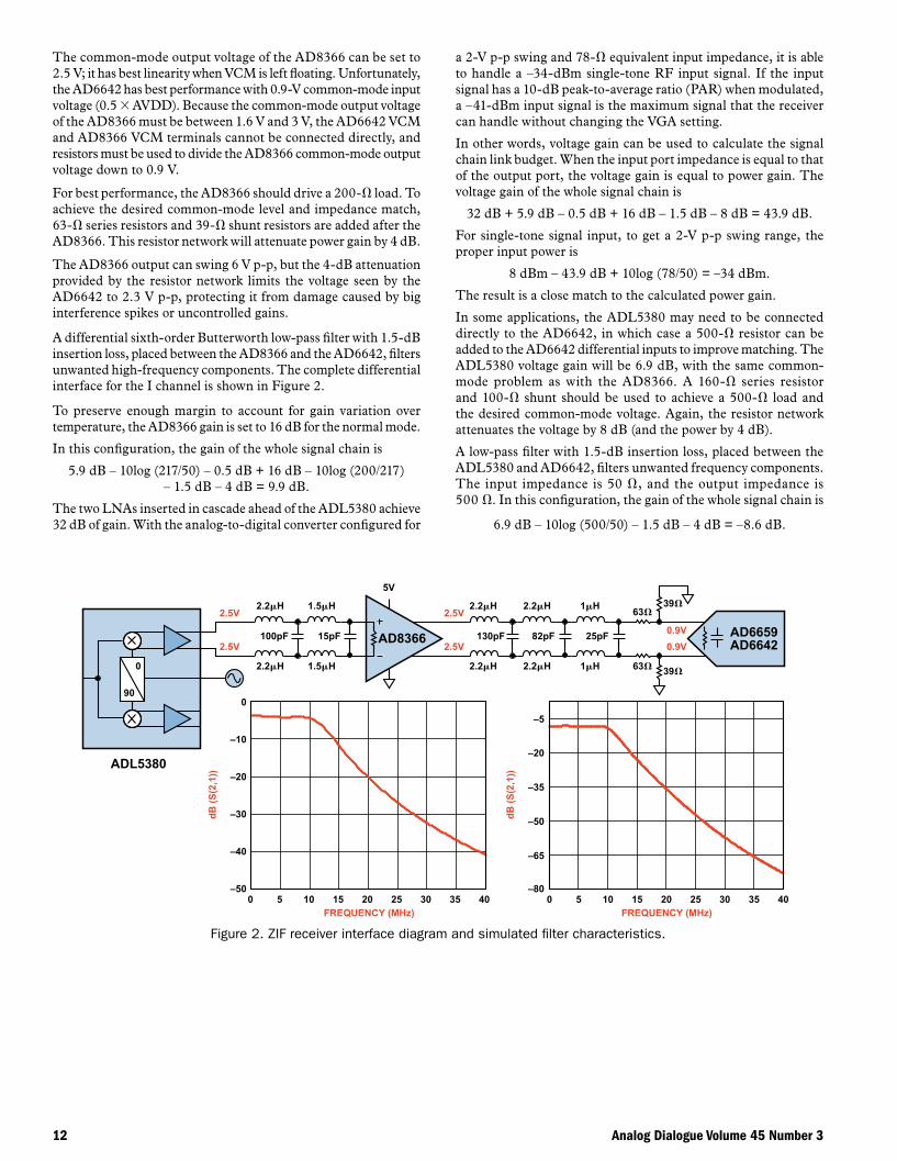
12 Analog Dialogue Volume 45 Number 3
The common-mode output voltage of the AD8366 can be set to 2.5 V; it has best linearity when VCM is left floating. Unfortunately, the AD6642 has best performance with 0.9-V common-mode input voltage (0.5 × AVDD). Because the common-mode output voltage of the AD8366 must be between 1.6 V and 3 V, the AD6642 VCM and AD8366 VCM terminals cannot be connected directly, and resistors must be used to divide the AD8366 common-mode output voltage down to 0.9 V.
For best performance, the AD8366 should drive a 200-Ω load. To achieve the desired common-mode level and impedance match, 63-Ω series resistors and 39-Ω shunt resistors are added after the AD8366. This resistor network will attenuate power gain by 4 dB.
The AD8366 output can swing 6 V p-p, but the 4-dB attenuation provided by the resistor network limits the voltage seen by the AD6642 to 2.3 V p-p, protecting it from damage caused by big interference spikes or uncontrolled gains.
A differential sixth-order Butterworth low-pass filter with 1.5-dB insertion loss, placed between the AD8366 and the AD6642, filters unwanted high-frequency components. The complete differential interface for the I channel is shown in Figure 2.
To preserve enough margin to account for gain variation over temperature, the AD8366 gain is set to 16 dB for the normal mode.
In this configuration, the gain of the whole signal chain is
5.9 dB – 10log (217/50) – 0.5 dB + 16 dB – 10log (200/217) – 1.5 dB – 4 dB = 9.9 dB.
The two LNAs inserted in cascade ahead of the ADL5380 achieve 32 dB of gain. With the analog-to-digital converter configured for
a 2-V p-p swing and 78-Ω equivalent input impedance, it is able to handle a –34-dBm single-tone RF input signal. If the input signal has a 10-dB peak-to-average ratio (PAR) when modulated, a –41-dBm input signal is the maximum signal that the receiver can handle without changing the VGA setting.
In other words, voltage gain can be used to calculate the signal chain link budget. When the input port impedance is equal to that of the output port, the voltage gain is equal to power gain. The voltage gain of the whole signal chain is
32 dB + 5.9 dB – 0.5 dB + 16 dB – 1.5 dB – 8 dB = 43.9 dB.
For single-tone signal input, to get a 2-V p-p swing range, the proper input power is
8 dBm – 43.9 dB + 10log (78/50) = –34 dBm.
The result is a close match to the calculated power gain.
In some applications, the ADL5380 may need to be connected directly to the AD6642, in which case a 500-Ω resistor can be added to the AD6642 differential inputs to improve matching. The ADL5380 voltage gain will be 6.9 dB, with the same common-mode problem as with the AD8366. A 160-Ω series resistor and 100-Ω shunt should be used to achieve a 500-Ω load and the desired common-mode voltage. Again, the resistor network attenuates the voltage by 8 dB (and the power by 4 dB).
A low-pass filter with 1.5-dB insertion loss, placed between the ADL5380 and AD6642, filters unwanted frequency components. The input impedance is 50 Ω, and the output impedance is 500 Ω. In this configuration, the gain of the whole signal chain is
6.9 dB – 10log (500/50) – 1.5 dB – 4 dB = –8.6 dB.
ADL5380
AD8366
0
900
–10
–20
–30
–40
–50
dB (S
(2,1
))
2.2�H 1.5�H
2.2�H
2.2�H
2.2�H
2.2�H
2.2�H
1�H
1�H 63�
63�
39�
39�
1.5�H
2.5V
2.5V
2.5V
2.5V0.9V0.9V
100pF 130pF 82pF15pF
5V
25pF
FREQUENCY (MHz)
–20
–5
–35
–50
–65
–800 5 10 15 20 25 30 35 400 5 10 15 20 25 30 35 40
dB (S
(2,1
))
FREQUENCY (MHz)
AD6659AD6642
Figure 2. ZIF receiver interface diagram and simulated filter characteristics.

Analog Dialogue Volume 45 Number 3 13
Superheterodyne Receiver Interface Design and Gain CalculationIn superheterodyne receivers, the system uses ac coupling, so the dc common-mode voltage does not have to be considered when interfacing these circuits.
Many mixers, such as the ADL535x and ADL580x, have 200-Ω differential output impedance, so the power gain and voltage gain are presented separately for different output impedances.
Figure 3 shows one channel of a superheterodyne receiver implemented with an ADL5523 low-noise amplif ier; an ADL5356 dual balanced mixer with LO buffer, IF amplifier, and RF balun; a low-pass filter; an AD8376 dual ultralow distortion IF VGA; another low-pass filter; and an AD6642 dual IF receiver.
This design uses a 140-MHz IF and 20-MHz bandwidth, so the parts can be ac-coupled.
The AD5356 has best performance with a 200-Ω load, but the AD8376 has 150-Ω input impedance. Thus, to suppress mixer output spurs and provide better impedance matching, the differential LC filter must have 200-Ω input impedance and 150-Ω output impedance. In applications where the output band signal must be suppressed by a sharp filter, a differential SAW filter can be used, but this introduces loss and group delay in the receiver signal chain. A differential fourth-order band-pass Butterworth filter may be suitable for many wireless receivers because the RF filter can provide enough attenuation for out-of-band interference.
Table 3. ADL5356 and AD8376 Interface and Gain Parameters
ADL5356 Test Conditions
VS = 5 V, TA = 25∙C, fRF = 1900 MHz, fLO = 1760 MHz, LO power = 0 dBm.
Parameters Values Comments
Voltage Conversion Gain
14.5 dB ZSOURCE = 50 Ω differential ZLOAD = 200 Ω differential
Power Conversion Gain
8.2 dB Including 4:1 IF port transformer and PCB loss
AD8376 Test Conditions
VS = 5 V, TA = 25∙C, RS = RL = 150 𝛀 at 140 MHz
Parameters Values Comments
Differential Input Resistance
150 Ω
Voltage Conversion Gain
–4 dB Minimum digital setting
20 dB Maximum digital setting
Output Impedance
16 kΩ||0.8 pF
ADF4350LO
ADL5523LOW-NOISEAMPLIFIER
MIXER WITHLO BUFFER,
IF AMPLIFIER,AND RF BALUN
LOW-DISTORTIONIF VGA IF RECEIVER
AD83761/2
AD6642AD6659
1/2ADL5356
Figure 3. Superheterodyne receiver diagram; one channel shown.
0
–10
–20
–30
–60
–50
–40
–70
dB (S
(2,1
))dB
(S(1
,1))
1�H1�H
1�H
1�H
82nH
82nH
150nH
150nH
120nH 12pF
12pF
470nH
120nH
6.8pF 6.8pF 2.2pF
330nH
330nH
330nH
56nH
33�165�
165� 33�330nH
3.3pF 20pF
CML
0 50 450400350300250200150100 550500 600
AD8376
5V5V
5V
AD6659AD6642
5V
5V
18pF 470nH
470pH18pF
210nH 470nH 300�
FREQUENCY (MHz)
0
–5
–10
–15
–30
–35
–40
–25
–20
–45
dB (S
(1,1
))dB
(S(2
,1))
20 40 2202001801601401201008060 260240 280FREQUENCY (MHz)
Figure 4. Superheterodyne receiver interface diagram and filter simulation result.

14 Analog Dialogue Volume 45 Number 3
The AD8376’s current-output circuit has high output impedance, so 150-Ω is needed between its differential outputs. Another differential filter must attenuate the second- and third-harmonic distortion components, so this 150-Ω load is divided into two parts. First, a 300-Ω resistor is installed in the output of the AD8376. Another 300-Ω resistor is formed by two 165-Ω resistors and the ADC’s 3-kΩ input impedance. The two 165-Ω resistors also provide the dc common-mode voltage for the ADC input. The LC filter’s input and output impedances are both 300 Ω. Perfect source and load matching is very important for high-IF applications. The complete interface is shown in Figure 4.
In the receiver, a 20-dB LNA is installed ahead of the mixer. The filter after the mixer has 2-dB insertion loss; the filter between the AD8376 and the ADC has 1.2-dB insertion loss. The AD8376 gain is set to 14 dB to provide enough margin to account for temperature variation. The overall gain of the receiver is
20 dB + 8.2 dB – 2 dB + 14 dB – 1.2 dB = 39 dB.
To limit the ADC input voltage to less than 2 V p-p, the power transmitted to the 150-Ω resistance (300 Ω || (165 Ω × 2) || 3 kΩ) should be smaller than 5.2 dBm. The maximum input power for the receiver is thus –33.8 dBm for a single-tone signal. If the input signal is a 10-dB PAR modulation signal, the maximum input signal using this gain setting is –40.8 dBm.
Transmitter Interface Design and Gain CalculationFor Tx-channel designs, both ZIF and superheterodyne architectures have similar interface characteristics, and both need dc coupling between the TxDAC® and the modulator. Most modulators’ IF input circuits should be biased by a dc voltage externally; the TxDAC output can provide dc bias for the modulator in a dc-coupled mode. Most high-speed DACs have current outputs, so an output resistor is needed to produce an output voltage for the modulator.
Figure 5 shows a superheterodyne or ZIF t ransmit ter implemented with an AD9122 TxDAC, a low-pass f ilter,
an ADL537x quadrature modulator, another RF filter, an ADF4350 synthesizer, an ADL5243 digitally controlled VGA, a power amplifier, and an AD562x DAC to control the power amplifier’s (PA) gate voltage.
For the AD9122, the full-scale output current can be set between 8.66 mA and 31.66 mA. For full-scale currents greater than 20 mA, the spurious-free dynamic range (SFDR) is decreased, but the output power and ACPR of the DAC decrease with lower full-scale current settings. A suitable compromise is a 0-mA to 20-mA current output consisting of a 20-mA ac current riding on a 10-mA dc level.
Table 4. AD9122 and ADL5372 Interface and Gain Parameters
AD9122 Test Conditions
AVDD33 = 3.3 V, DVDD33 = 3.3 V, DVDD18 = 1.8 V, CVDD18 = 1.8 V
Parameters Values Comments
Full-Scale Output Current
8.66 mA Minimum digital full-scale setting
31.66 mA Maximum digital full-scale setting
Output Resistance
10 MΩ
ADL5372 Test Conditions
VS = 5 V, TA = 25°C, fLO = 1900 MHz, f IF = 140 MHz
Parameters Values Comments
Output Power 7.1 dBm VIQ = 1.4 V p-p differential
I and Q Input Bias Level
0.5 V Recommended
Differential Input Impedance
2900 kΩ
ADL537x
AD562x
ADL5243DIGITALLY CONTROLLED VGA
ADF4350
LO
DAC
DAC
AD9122
DUALTxDAC
QUADMODULATOR
0
90
DAC
PA GATEVOLTAGE CONTROL
PA
Figure 5. Transmitter diagram.

Analog Dialogue Volume 45 Number 3 15
The input circuit of the ADL5372 needs a 0.5-V common-mode voltage, which is provided by a 10-mA dc current flowing through a 50-Ω resistor. The 0-mA to 20-mA ac current is shared by two 50-Ω resistors and a 100-Ω resistor. The ac voltage between the modulator inputs is thus 20 mA × ((50 × 2) || 100) = 1 V p-p. The filter between the TxDAC and the modulator removes unwanted frequency components. The input and output impedance of the filter is 100 Ω. The complete interface is shown in Figure 6.
With a 50-Ω output, the voltage conversion gain of the ADL5372 is 0.2 dBm. With a 13-dB PAR modulator signal, the average power must be reduced by at least 15 dB for the Tx digital predistortion process. With a 1-V p-p single-tone input to the ADL5372, the average modulator output power is 7.1 dBm – 2.9 dBm = 4.2 dBm. If the 2.2-dBm insertion loss of the low-pass filter is considered, the peak output power is 4.2 dBm – 2.2 dBm = 2 dBm. In this state, an average output power of –10 dBm is presented at the output of the modulator.
With an 11-dBm average power signal, a PA-driver with 26-dBm P1dB is needed in the Tx signal chain. If a 2-dB insertion-loss RF filter is needed to suppress LO feedthrough and sideband output of the modulator, then the gain block and PA driver have to provide a total of 21-dB gain. The ADL5243 VGA with integrated gain block, digitally controlled attenuator, and PA driver is suggested for this application.
ConclusionThis paper describes ZIF and superheterodyne receiver differential interfaces for the demodulator, IF VGA, mixer, and analog port of the ADC, as well as transmitter differential interfaces between the TxDAC and FMOD, using Analog Devices parts for active portions of the signal chain. Gain calculations and simulation results are presented for the application filters that were designed for these circuits. Additional information can be found in the following references.
ReferencesCircuit Note CN-0018, Interfacing the ADL5372 I/Q Modulator to the AD9779A Dual-Channel, 1 GSPS High-Speed DAC.Circuit Note CN-0134, Broadband Low Error Vector Magnitude (EVM) Direct Conversion Transmitter.Calvo, Carlos. “The di f ferent ia l-signal advantage for communications system design.” EE Times. Feb 2010.
AuthorMingming Zhao [[email protected]] is a field applications engineer for ADI North China in Beijing, China. Mingming mainly supports RF and high-speed converter product applications. After earning a master’s degree in electromagnetic and microwave technology from the Chinese Academy of Sciences, and spending more than two years as an RF engineer at Datang Mobile Telecommunication Equipment Co, Ltd., Mingming joined Analog Devices in 2010.
ADL537x
0
90
I DACOR Q DAC
50�
50�
100�
22pF
22pF
2pF 25pF
3pF
3pF
33nH 56nH
33nH 56nH
–10
0
–20
–30
–40
–500 100 200 300 400 500 600 700 800
dB (S
(1,1
))dB
(S(2
,1))
FREQUENCY (MHz)
Figure 6. DC coupled transmitter IF interface diagram and filter simulation result.

16 Analog Dialogue Volume 45 Number 3
How to Apply DC-to-DC Step-Up (Boost) Regulators SuccessfullyBy Ken MarascoPower for portable electronic devices such as smartphones, GPS navigation systems, and tablets can come from low-voltage solar panels, batteries, or ac-to-dc power supplies. Battery-powered systems often stack cells in series to achieve higher voltages, but this is not always possible due to a lack of space. Switching converters use an inductor’s magnetic field to alternately store energy and release it to the load at a different voltage. With low losses they are a good choice for high efficiency. Capacitors connected to the converter’s output reduce output voltage ripple. Boost, or step-up, converters—covered here—provide higher voltage; buck, or step-down, converters—covered in a previous article1—provide lower output voltage. Switching converters that include internal FETs as switches are called switching regulators,2 while devices requiring external FETs are called switching controllers.3
Figure 1 shows a typical low-power system powered from two series-connected AA batteries. The battery’s usable output varies from about 1.8 V to 3.4 V, whereas the ICs require 1.8 V and 5.0 V to operate. Boost converters, which can step up the voltage without increasing the number of cells, power the WLED backlights, micro hard disk drives, audio, and USB peripherals, while a buck converter powers the microprocessor, memory, and display.
The inductor’s tendency to resist changes in current enables the boost function. When charging, the inductor acts as a load and stores energy; when discharging, it acts as an energy source. The voltage produced during the discharge phase is related to the current’s rate of change, not to the original charging voltage, thus allowing different input and output voltage levels.
Boost regulators consist of two switches, two capacitors, and an inductor, as shown in Figure 2. Nonoverlapping switch drives ensure that only one switch is on at a time to avoid unwanted shoot-through current. In Phase 1 (tON), Switch B is open and
Switch A is closed. The inductor is connected to ground, so current flows from VIN to ground. The current increases due to the positive voltage across the inductor, and energy is stored in the inductor. In Phase 2 (tOFF), Switch A is open and Switch B is closed. The inductor is connected to the load, so current flows from VIN to the load. The current decreases due to the negative voltage across the inductor, and energy stored in the inductor is discharged into the load.
VIN CIN
COUT
COUT
ION
L
A
VSWVOUT
BPWM ON
LOAD
+
VIN CINIOFF
L
A
VSW VOUTBPWM OFF
LOAD
+
IL
IL
VIN
VOUT
ION
VSW
IOFF
IL
�IL
PWMMODULATION
tONt
tOFF
Figure 2. Buck converter topology and operating waveforms.
MEMORY
AUDIO
BOOSTREGULATORADP8866
BOOSTREGULATORADP1612
USBTRANSCEIVER
LOADSWITCHADP195
BUCKREGULATORADP2138
1.8V TO 3.4VBATTERY PACK
SPEAKERS 5V
1.8V
MICRO HDD
MICROPROCESSOR
LCDDISPLAY
Figure 1. Typical low-power portable system.

Analog Dialogue Volume 45 Number 3 17
Note that the switching regulator operation can be continuous or discontinuous. When operating in continuous conduction mode (CCM), the inductor current never drops to zero; when operating in discontinuous conduction mode (DCM), the inductor current can drop to zero. The current ripple, shown as ΔIL in Figure 2, is calculated using ΔIL = (VIN × tON)/L. The average inductor current flows into the load, while the ripple current flows into the output capacitor.
VIN
VSW
R2 R1
CIN
COUT
VOUT
+ IOFF
ILOSCILLATOR
BA
LOAD
PWMCONTROLCURRENT
LIMIT
FB
L
Figure 3. Boost regulator integrates oscillator, PWM control loop, and switching FETs.
Regulators that use a Schottky diode in place of Switch B are defined as asynchronous (or nonsynchronous), while regulators that use a FET as Switch B are defined as synchronous. In Figure 3, Switches A and B have been implemented with an internal NFET and an external Schottky diode, respectively, to create an asynchronous boost regulator. For low-power applications requiring load isolation and low shutdown current, external FETs can be added, as shown in Figure 4. Driving the device’s EN pin below 0.3 V shuts down the regulator and completely disconnects the input from the output.
ADP1612/ADP1613
6
3
7
8
5
2
1
4
VIN
EN
FREQ
SS
SW
FB
COMPGND
1.3MHz650kHz
(DEFAULT)
VOUT
L1
CIN
CSSCOUT
CCOMP
RCOMP
R1
R2
D1VIN
R310k�
Q1A
BQ1
ONOFF
Figure 4. ADP1612/ADP1613 typical applications circuit.
Modern low-power synchronous buck regulators use pulse-width modulation (PWM) as the primary operating mode. PWM holds the frequency constant and varies the pulse width (tON) to adjust the output voltage. The average power delivered is proportional to the duty cycle, D, making this an efficient way to provide power to a load.
As an example, for a desired output voltage of 15 V and an available input voltage of 5 V,
D = (15 – 5)/15 = 0.67 or 67%.
Energy is conserved, so the input power must equal the power delivered to the load minus any losses. Assuming very efficient conversion, the small amount of power lost can be omitted from the basic power calculations. The input current can thus be approximated by
For example, if the load current is 300 mA at 15 V, IIN = 900 mA at 5 V—three times the output current. Therefore, the available load current decreases as the boost voltage increases.
Boost converters use either voltage- or current feedback to regulate the selected output voltage; the control loop enables the output to maintain regulation in response to load changes. Low power boost regulators generally operate between 600 kHz and 2 MHz. The higher switching frequencies allow use of smaller inductors, but the efficiency drops by approximately 2% with every doubling of the switching frequency. In the ADP1612 and ADP1613 boost converters (see Appendix), the switching frequency is pin-selectable, operating at 650 kHz for highest efficiency or at 1.3 MHz for smallest external components. Connect FREQ to GND for 650-kHz operation or to VIN for 1.3-MHz operation.
The inductor, a key component of the boost regulator, stores energy during the on time of the power switch and transfers that energy to the output through the output rectifier during the off time. To balance the trade-offs between low inductor current ripple and high efficiency, the ADP1612/ADP1613 data sheet recommends inductance values in the 4.7-µH to 22-µH range. In general, a lower value inductor has a higher saturation current and a lower series resistance for a given physical size, but lower inductance results in higher peak currents that can lead to reduced efficiency, higher ripple, and increased noise. It is often better to run the boost in discontinuous conduction mode to reduce the inductor size and improve stability. The peak inductor current (the maximum input current plus half the inductor ripple current) must be lower than the rated saturation current of the inductor; and the maximum dc input current to the regulator must be less than the inductor’s rms current rating.
Key Boost Regulator Specifications and DefinitionsInput Voltage Range: A boost converter’s input voltage range determines the lowest usable input supply voltage. The specifications may show a wide input voltage range, but the input voltage must be lower than VOUT for efficient operation.
Ground or Quiescent Current: The dc bias current not delivered to the load (Iq). The lower the Iq the better the efficiency, but Iq can be specified under many conditions, including switching off, zero load, PFM operation, or PWM operation, so it is best to look at operating efficiency at specific operating voltages and load currents to determine the best boost regulator for the application.
Shutdown Current: The input current consumed when the enable pin has been set to OFF. Low Iq is important for long standby times when a battery-powered device is in sleep mode.
Switch Duty Cycle: The operating duty cycle must be lower than the maximum duty cycle or the output voltage will not be regulated. For example, D = (VOUT – VIN)/VOUT. With VIN = 5 V and VOUT = 15 V, D = 67%. The ADP1612 and ADP1613 have a maximum duty cycle of 90%.
Output Voltage Range: The range of output voltages the device will support. The boost converter’s output voltage can be fixed or adjustable, using resistors to set the desired output voltage.
Current Limit: Boost converters usually specify peak current limit, not load current. Note that the greater the difference between VIN and VOUT, the lower the available load current. The peak current limit, input voltage, output voltage, switching frequency, and inductor value all set the maximum available output current.
Line Regulation: Line regulation is the change in output voltage caused by a change in the input voltage.

18 Analog Dialogue Volume 45 Number 3
Load Regulation: Load regulation is the change in output voltage for a change in the output current.
Soft Start: It is important for boost regulators to have a soft-start function that ramps the output voltage in a controlled manner upon startup to prevent excessive output voltage overshoot at startup. The soft start of some boost converters can be adjusted by an external capacitor. As the soft-start capacitor charges, it limits the peak current allowed by the part. With adjustable soft start, the start-up time can be changed to meet system requirements.
Thermal Shutdown (TSD): If the junction temperature rises above the specified limit, the thermal shutdown circuit turns the regulator off. Consistently high junction temperatures can be the result of high-current operation, poor circuit board cooling, or high ambient temperature. The protection circuit includes hysteresis so that the device will not return to normal operation until the on-chip temperature drops below the preset limit after thermal shutdown occurs.
Undervoltage Lockout (UVLO): If the input voltage is below the UVLO threshold, the IC automatically turns off the power switch and goes into a low-power mode. This prevents potentially erratic operation at low input voltages and prevents the power device from turning on when the circuitry cannot control it.
ConclusionLow-power boost regulators take the worry out of switching dc-to-dc converter design by delivering a proven design. Design calculations are available in the applications section of the data sheet, and the ADIsimPower4 design tool simplifies the task for the end user. For additional information, please contact the applications engineers at Analog Devices, or visit the EngineerZone at ez.analog.com for help. Analog Devices boost-regulator selection guides, data sheets, and application notes can be found at www.analog.com/power.
References(Information on all ADI components can be found at www.analog.com.)
1 www.analog.com/library/analogDialogue/archives/45-06/buck_regulators.html.
2 www.analog.com/en/power-management/switching-regulators-integrated-fet-switches/products/index.html.
3 www.analog.com/en/power-management/switching-controllers-external-switches/products/index.html.
4 http://designtools.analog.com/dtPowerWeb/dtPowerMain.aspx
Lenk, John D. Simplified Design of Switching Power Supplies. Elsevier/Newnes. 1996.
Marasco, K. “How to Apply DC-to-DC Step-Down (Buck) Regulators Successfully.” Analog Dialogue. Volume 45. June 2011.
Marasco, K. “How to Apply Low-Dropout Regulators Successfully.” Analog Dialogue. Volume 43, Number 3. 2009.
AuthorKen Marasco [[email protected]] is a system applications manager. Responsible for the technical support of portable power products, he has been a member of the Analog Devices Portable Applications Team for three years. He graduated from NYIT with a degree in applied physics and has 35 years of system and component design experience.
APPENDIxStep-Up DC-to-DC Switching Converters Operate at 650 kHz/1300 kHzThe ADP1612 and ADP1613 step-up converters are capable of supplying over 150 mA at voltages as high as 20 V, while operating, respectively, with a single 1.8-V to 5.5-V and 2.5-V to 5.5-V supply. Integrating a 1.4-A/2.0-A, 0.13-Ω power switch with a current-mode, pulse-width modulated regulator, their output varies less than 1% with changes in input voltage, load current, and temperature. The operating frequency is pin-selectable and can be optimized for high efficiency or minimum external component size: at 650 kHz they provide 90% efficiency; at 1.3 MHz their circuit implementation occupies the smallest space, making them ideal for space-constrained environments in portable devices and liquid-crystal displays. The adjustable soft-start circuit prevents inrush currents, ensuring safe, predictable start-up conditions. The ADP1612 and ADP1613 consume 2.2 mA in the switching state, 700 µA in the nonswitching state, and 10 nA in shutdown mode. Available in 8-lead MSOP packages, they are specified from –40°C to +85°C and priced at $1.50/$1.20 in 1000s.
FREQ
SW
PWMCOMPARATOR
UVLOCOMPARATOR
TSDCOMPARATOR
OSCILLATOR
S
RQ
DCOMPARATOR
DREF
+
+
7VIN
CURRENTSENSING
5�A
DRIVER
BAND GAP
N1
BGRESET
1.1M�
AGND
VIN
UVLOREF
TSENSE
TREF
ERRORAMPLIFIER
VBG
SOFTSTART
2
1
5�A
VSS
RCOMP
CCOMP
COMP
SS
FB
CSS
R1
R2
CIN
VOUT
6
VIN
L1
D1A VOUT
COUT
5
3 4GND
AGND
>1.6VEN
ADP1612/ADP1613
8
VIN
<0.3V
>1.6V
<0.3V
Figure A. ADP1612/ADP1613 functional block diagram.

Analog Dialogue Volume 45 Number 3 19
System Demonstration Platform Facilitates Quick Prototyping and EvaluationBy Rosemary Ryan
System design can be a complex problem with many different elements to comprehend, but the ability to prototype and quickly demonstrate subsections of the solution can simplify the process and, more importantly, reduce the risks faced by designers. With the Analog Devices (ADI) System Demonstration Platform (SDP), system designers can reuse central elements, allowing subsections of their designs to be evaluated and demonstrated prior to the final system implementation. Component and reference circuit evaluation boards from across ADI’s portfolio are now available on the SDP, with more becoming available all the time. The familiarity gained from prior use of the platform makes it easy for users to evaluate new categories of components in an environment they already know and understand. The SDP connects to FPGA evaluation and prototyping platforms, allowing easy creation and demonstration of customized FPGA embedded designs that communicate with ADI components. Users can build customized evaluation and prototyping systems quickly, and the ability to reuse various platform elements makes demonstrating a wide variety of hardware and software concepts easy and affordable.
Platform OverviewAs shown in Figure 1, the System Demonstration Platform comprises a series of controller boards, interposer boards, and daughter boards that implement an easy to use evaluation system for ADI components and reference circuits that use them. Controller boards connect to a PC through a USB 2.0 link and to SDP-compatible daughter boards via on-board connectors. Daughter boards include dedicated component evaluation boards and Circuits from the Lab™ reference circuits. Interposer boards connect controller boards to daughter boards, or adapt SDP daughter boards to third-party tools. A standard, small-footprint, 120-pin connector with defined pinout is common to all boards in the platform, allowing a customized system to be built and altered easily. Controller boards have a 120-pin connector header; daughter boards have a receptacle connector; and interposer boards have a header, a receptacle, or both, depending on their functionality.
USB PLUG
SDP DAUGHTERBOARDS
THIRD-PARTYDESIGN TOOLSINTERPOSER BOARDS
CONTROLLERBOARDS
EVALUATIONSYSTEM
SIGNAL MONITORINGON EVALUATION SYSTEM
EVALUATING WITHTHIRD-PARTY TOOLS
Figure 1. System Demonstration Platform overview.
Controller BoardsThe two types of controller boards, the SDP-B and the SDP-S, are shown in Figure 2. Both require a USB 2.0 link for control and data transfer between the system and the PC-based user interface.
Figure 2. Controller boards: a) SDP-B. b) SDP-S.
The SDP-B, with an ADSP-BF527 Blackfin® processor at its core, is a small-form-factor board that uses a USB mini-B connector for PC connectivity, as shown in Figure 3. The Blackfin processor functions as the USB controller, and also provides a range of peripheral interfaces to the daughter board. Available via two identical 120-pin connectors, these interfaces include SPI, SPORT, I2C, GPIOs, timers, PPI, and asynchronous parallel. The SDP-B controller can be used with any daughter board designed for the SDP. The two 120-pin connectors facilitate simultaneous connection of two daughter boards to a single controller board.
Figure 3. SDP-B controller functional overview.
The SDP-S, a small, low-cost, serial-only controller board provides a reduced set of peripheral interfaces as compared to the SDP-B. With a USB-to-serial engine at its core, the SDP-S has a single 120-pin connector that is pin-compatible with the connectors on the SDP-B. Its subset of peripheral interfaces includes SPI, I2C, and GPIOs. All boards designed to work with the SDP-S will work with the SDP-B, as the SDP-B provides a superset of the SDP-S capabilities. Table 1 compares the peripheral interfaces available with SDP-B and SDP-S boards.
Table 1. Controller Boards
Peripheral Interface SDP-B SDP-S
SPI • •
SPORT •
GPIO • •
I2C • •
Asynchronous Parallel •
PPI •
Timers •
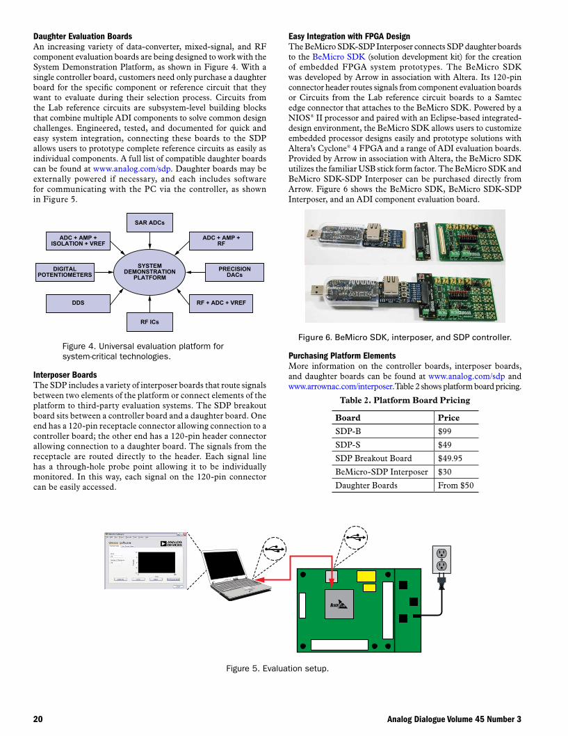
20 Analog Dialogue Volume 45 Number 3
Daughter Evaluation BoardsAn increasing variety of data-converter, mixed-signal, and RF component evaluation boards are being designed to work with the System Demonstration Platform, as shown in Figure 4. With a single controller board, customers need only purchase a daughter board for the specific component or reference circuit that they want to evaluate during their selection process. Circuits from the Lab reference circuits are subsystem-level building blocks that combine multiple ADI components to solve common design challenges. Engineered, tested, and documented for quick and easy system integration, connecting these boards to the SDP allows users to prototype complete reference circuits as easily as individual components. A full list of compatible daughter boards can be found at www.analog.com/sdp. Daughter boards may be externally powered if necessary, and each includes software for communicating with the PC via the controller, as shown in Figure 5.
ADC + AMP +ISOLATION + VREF
DDS
DIGITALPOTENTIOMETERS
ADC + AMP +RF
RF + ADC + VREF
PRECISIONDACs
SAR ADCs
RF ICs
SYSTEMDEMONSTRATION
PLATFORM
Figure 4. Universal evaluation platform for system-critical technologies.
Interposer BoardsThe SDP includes a variety of interposer boards that route signals between two elements of the platform or connect elements of the platform to third-party evaluation systems. The SDP breakout board sits between a controller board and a daughter board. One end has a 120-pin receptacle connector allowing connection to a controller board; the other end has a 120-pin header connector allowing connection to a daughter board. The signals from the receptacle are routed directly to the header. Each signal line has a through-hole probe point allowing it to be individually monitored. In this way, each signal on the 120-pin connector can be easily accessed.
Easy Integration with FPGA DesignThe BeMicro SDK-SDP Interposer connects SDP daughter boards to the BeMicro SDK (solution development kit) for the creation of embedded FPGA system prototypes. The BeMicro SDK was developed by Arrow in association with Altera. Its 120-pin connector header routes signals from component evaluation boards or Circuits from the Lab reference circuit boards to a Samtec edge connector that attaches to the BeMicro SDK. Powered by a NIOS® II processor and paired with an Eclipse-based integrated-design environment, the BeMicro SDK allows users to customize embedded processor designs easily and prototype solutions with Altera’s Cyclone® 4 FPGA and a range of ADI evaluation boards. Provided by Arrow in association with Altera, the BeMicro SDK utilizes the familiar USB stick form factor. The BeMicro SDK and BeMicro SDK-SDP Interposer can be purchased directly from Arrow. Figure 6 shows the BeMicro SDK, BeMicro SDK-SDP Interposer, and an ADI component evaluation board.
Figure 6. BeMicro SDK, interposer, and SDP controller.
Purchasing Platform ElementsMore information on the controller boards, interposer boards, and daughter boards can be found at www.analog.com/sdp and www.arrownac.com/interposer. Table 2 shows platform board pricing.
Table 2. Platform Board Pricing
Board Price
SDP-B $99
SDP-S $49
SDP Breakout Board $49.95
BeMicro-SDP Interposer $30
Daughter Boards From $50
Figure 5. Evaluation setup.

Analog Dialogue Volume 45 Number 3 21
its effectiveness as a reusable, customizable system demonstrator and prototype builder increases. The diversity of available daughter boards, including both component evaluation boards and Circuits from the Lab reference circuits, ensures that the System Demonstration Platform can provide a one-stop solution to a designer’s evaluation and demonstration needs. Visit www.analog.com/sdp to keep up to date with all the latest news and releases on the SDP.
AuthorRosemary Ryan [[email protected]] is an applications engineer with the Precision System Applications team. She graduated from the University of Limerick with a BEng in computer engineering in 2005 and joined ADI in Limerick in 2006. In 2010 she graduated from Waterford Institute of Technology with an MEng in Electronic Engineering. She currently works as part of the team responsible for the development of the System Demonstration Platform (SDP).
Future ModulesWith the goal of simplifying the system design process by providing easy-to-use demonstration and evaluation elements that solve a growing set of problems, the System Demonstration Platform will continue to evolve and expand. In September 2011, System Function Modules will be added to the platform to provide additional functionality to the existing platform. The first module will be an FPGA module. The SDP-FPGA module will sit between a controller board and a daughter board, increasing the flexibility of a demonstration or prototype system. The SDP-FPGA module will connect to the 120-pin connector on the controller board and will have a 120-pin header connector for connection to daughter boards. The SDP-FPGA board will also have a differential connector, allowing components with differential signaling interfaces to be included on the SDP platform.
ConclusionThe System Demonstration Platform provides system designers with a level of flexibility previously unavailable from a single ADI platform. As the platform continues to grow and develop,
FPGA
DIFFERENTIALCONNECTOR
Figure 7. FPGA system function module.
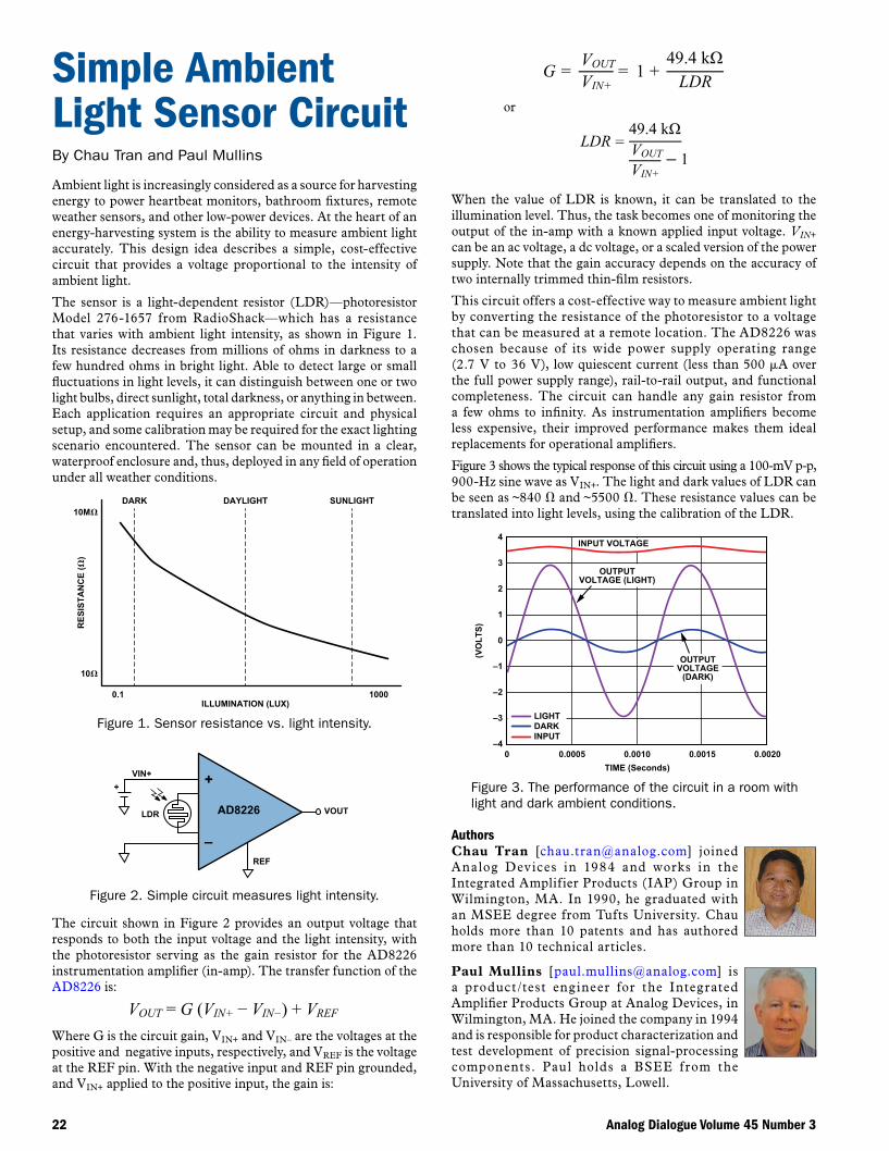
22 Analog Dialogue Volume 45 Number 3
or
When the value of LDR is known, it can be translated to the illumination level. Thus, the task becomes one of monitoring the output of the in-amp with a known applied input voltage. VIN+ can be an ac voltage, a dc voltage, or a scaled version of the power supply. Note that the gain accuracy depends on the accuracy of two internally trimmed thin-film resistors.
This circuit offers a cost-effective way to measure ambient light by converting the resistance of the photoresistor to a voltage that can be measured at a remote location. The AD8226 was chosen because of its wide power supply operating range (2.7 V to 36 V), low quiescent current (less than 500 µA over the full power supply range), rail-to-rail output, and functional completeness. The circuit can handle any gain resistor from a few ohms to infinity. As instrumentation amplifiers become less expensive, their improved performance makes them ideal replacements for operational amplifiers.
Figure 3 shows the typical response of this circuit using a 100-mV p-p, 900-Hz sine wave as VIN+. The light and dark values of LDR can be seen as ~840 Ω and ~5500 Ω. These resistance values can be translated into light levels, using the calibration of the LDR.
4
–4
–3
–2
–1
0
1
2
3
0 0.0005 0.0010 0.0015 0.0020
(VO
LTS)
TIME (Seconds)
INPUT VOLTAGE
OUTPUTVOLTAGE (LIGHT)
OUTPUTVOLTAGE
(DARK)
LIGHTDARKINPUT
Figure 3. The performance of the circuit in a room with light and dark ambient conditions.
AuthorsChau Tran [[email protected]] joined Analog Dev ices in 1984 and works in the Integrated Amplif ier Products (IAP) Group in Wilmington, MA. In 1990, he graduated with an MSEE degree from Tufts University. Chau holds more than 10 patents and has authored more than 10 technical articles.
Paul Mullins [[email protected]] is a product /test eng ineer for the Integrated Amplifier Products Group at Analog Devices, in Wilmington, MA. He joined the company in 1994 and is responsible for product characterization and test development of precision signal-processing components. Paul holds a BSEE f rom the University of Massachusetts, Lowell.
Simple Ambient Light Sensor CircuitBy Chau Tran and Paul Mullins
Ambient light is increasingly considered as a source for harvesting energy to power heartbeat monitors, bathroom fixtures, remote weather sensors, and other low-power devices. At the heart of an energy-harvesting system is the ability to measure ambient light accurately. This design idea describes a simple, cost-effective circuit that provides a voltage proportional to the intensity of ambient light.
The sensor is a light-dependent resistor (LDR)—photoresistor Model 276-1657 from RadioShack—which has a resistance that varies with ambient light intensity, as shown in Figure 1. Its resistance decreases from millions of ohms in darkness to a few hundred ohms in bright light. Able to detect large or small fluctuations in light levels, it can distinguish between one or two light bulbs, direct sunlight, total darkness, or anything in between. Each application requires an appropriate circuit and physical setup, and some calibration may be required for the exact lighting scenario encountered. The sensor can be mounted in a clear, waterproof enclosure and, thus, deployed in any field of operation under all weather conditions.
RES
ISTA
NC
E (�
)
ILLUMINATION (LUX)
DARK DAYLIGHT SUNLIGHT
0.1
10�
10M�
1000
Figure 1. Sensor resistance vs. light intensity.
AD8226
+
–
VOUT
REF
VIN++
LDR
Figure 2. Simple circuit measures light intensity.
The circuit shown in Figure 2 provides an output voltage that responds to both the input voltage and the light intensity, with the photoresistor serving as the gain resistor for the AD8226 instrumentation amplifier (in-amp). The transfer function of the AD8226 is:
Where G is the circuit gain, VIN+ and VIN– are the voltages at the positive and negative inputs, respectively, and VREF is the voltage at the REF pin. With the negative input and REF pin grounded, and VIN+ applied to the positive input, the gain is:

Analog Dialogue Volume 45 Number 3 23

©2011 Analog Devices, Inc. All rights reserved. Trademarks and registered trademarks are the property of their respective owners.
M02000453-0-9/11
www.analog.com/analogdialogue
Analog Devices, Inc.Worldwide HeadquartersAnalog Devices, Inc. One Technology Way P.O. Box 9106 Norwood, MA 02062-9106 U.S.A. Tel: 781.329.4700 (800.262.5643, U.S.A. only) Fax: 781.461.3113
Analog Devices, Inc. Europe HeadquartersAnalog Devices, Inc. Wilhelm-Wagenfeld-Str. 6 80807 Munich Germany Tel: 49.89.76903.0 Fax: 49.89.76903.157
Analog Devices, Inc. Japan HeadquartersAnalog Devices, KK New Pier Takeshiba South Tower Building 1-16-1 Kaigan, Minato-ku, Tokyo, 105-6891 Japan Tel: 813.5402.8200 Fax: 813.5402.1064
Analog Devices, Inc. Southeast Asia HeadquartersAnalog Devices 22/F One Corporate Avenue 222 Hu Bin Road Shanghai, 200021 China Tel: 86.21.2320.8000 Fax: 86.21.2320.8222