analysis of a physical layer wireless communication system implementation on an sdr
TRANSCRIPT

Analysis of a Physical Layer Wireless Communication System Implementation on an SDR Baseband Processor
BABAK D. BEHESHTI
School of Engineering and Technology New York Institute of Technology
Old Westbury, NY11568 U.S.A.
Abstract: - In this paper, implementation and analysis of an entire wireless communication system physical layer receiver in software is presented. The two paramount issues, namely real-time performance of the executable, as compared to hardware implementation performance, and the power consumption projections for the DSP executing the receiver code are presented. Issues investigated include the paradigm-shift from hardware centric algorithm realizations to a software centric methodology, fixed point DSP algorithm implementation in ANSI C, synchronization of receive and transmit events such as TDMA operations, and processing chain partitioning in a software defined radio baseband processing environment. Results presented will include the MIPS requirements of the processing chain, as well as code and data partitioning trade-offs. Key-Words: - Wireless, Physical layer, Baseband processing, Software Defined Radio, DPSK. 1 Introduction As the complexity of baseband processing algorithms for mobile communications increases to accommodate higher data rates and multi-media services, at the very same time the requirement for less expensive handsets is becoming more and more demanding on handset designers and manufacturers. These two opposing driving forces require a new approach to the mobile handset design, not required in the past where baseband processing was not as complex as current technologies. In any engineering activity, when complexity of design becomes high, the potential for design errors or “bugs” increases. Therefore inevitably, the handset manufacturers face serious and costly situations where after shipping of their handsets, a defect is discovered in the handset design, requiring a recall, and perhaps a very expensive campaign not only to replace the handsets, but also to mend the public opinion of the manufacturer, damaged by this problem. Handset designers have been addressing this issue for sometime, however the underlying baseband processing technology prohibited any substantial deviation from the classical approach taken by mobile equipment designers for the past twenty years. This classic approach has been as follows: 1. Design the algorithms in floating point arithmetic and analyze their behavior via simulation in presence of noise and other channel conditions. Enhance and finalize the algorithms. 2. Implement the same algorithms in fixed point, as floating-point operations are very expensive as far as
computation and power consumption are concerned. Enhance and iterate to get desirable performance. 3. Design hardware blocks to implement the above fixed point algorithms. 4. Proceed to chip design, building circuits on the Silicon to accommodate these blocks. This step is very lengthy and costly, typically taking around 18 months and millions of Dollars in cost. 5. Place chips in handsets and ship them. Should any bug be discovered after this stage, the entire process above needs to be repeated, causing enormous cost overruns. As long as baseband processing is locked into hardware blocks, the inherent problem discussed above remains unresolved. This study addresses the above issue by exploring an alternative approach to the classic one, namely an all software approach. This concept has been studied extensively recently and has been named “Software Defined Radio” or SDR. As the name implies, all algorithms and control code are implemented in software, running on a special purpose microprocessor, called a Digital Signal Processor (DSP). Therefore, the 18 month design cycle for the custom ASIC (Application Specific Integrated Circuit) is removed from the process, reducing the time-to-market to the handset manufacturer substantially as well as reducing the design costs. Moreover, should any design error or bug be discovered in the handset design after deployment in the field, a mere software download of the corrected software (over the air, via the Internet to an infrared
Proceedings of the 5th WSEAS Int. Conf. on Electronics, Hardware, Wireless and Optical Communications, Madrid, Spain, February 15-17, 2006 (pp26-29)
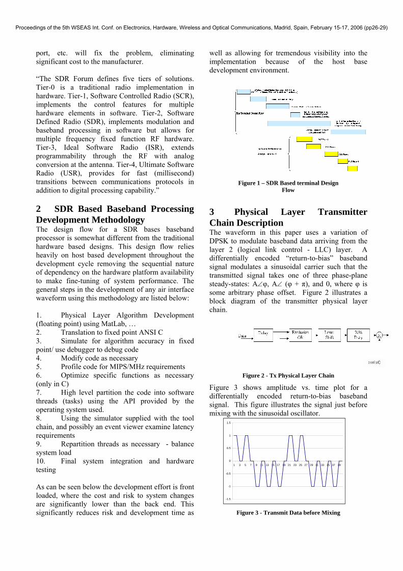
port, etc. will fix the problem, eliminating significant cost to the manufacturer. “The SDR Forum defines five tiers of solutions. Tier-0 is a traditional radio implementation in hardware. Tier-1, Software Controlled Radio (SCR), implements the control features for multiple hardware elements in software. Tier-2, Software Defined Radio (SDR), implements modulation and baseband processing in software but allows for multiple frequency fixed function RF hardware. Tier-3, Ideal Software Radio (ISR), extends programmability through the RF with analog conversion at the antenna. Tier-4, Ultimate Software Radio (USR), provides for fast (millisecond) transitions between communications protocols in addition to digital processing capability.” 2 SDR Based Baseband Processing Development Methodology The design flow for a SDR bases baseband processor is somewhat different from the traditional hardware based designs. This design flow relies heavily on host based development throughout the development cycle removing the sequential nature of dependency on the hardware platform availability to make fine-tuning of system performance. The general steps in the development of any air interface waveform using this methodology are listed below: 1. Physical Layer Algorithm Development (floating point) using MatLab, … 2. Translation to fixed point ANSI C 3. Simulate for algorithm accuracy in fixed point/ use debugger to debug code 4. Modify code as necessary 5. Profile code for MIPS/MHz requirements 6. Optimize specific functions as necessary (only in C) 7. High level partition the code into software threads (tasks) using the API provided by the operating system used. 8. Using the simulator supplied with the tool chain, and possibly an event viewer examine latency requirements 9. Repartition threads as necessary - balance system load 10. Final system integration and hardware testing As can be seen below the development effort is front loaded, where the cost and risk to system changes are significantly lower than the back end. This significantly reduces risk and development time as
well as allowing for tremendous visibility into the implementation because of the host base development environment.
Figure 1 – SDR Based terminal Design Flow
3 Physical Layer Transmitter Chain Description The waveform in this paper uses a variation of DPSK to modulate baseband data arriving from the layer 2 (logical link control - LLC) layer. A differentially encoded “return-to-bias” baseband signal modulates a sinusoidal carrier such that the transmitted signal takes one of three phase-plane steady-states: A∠φ, A∠ (φ + π), and 0, where φ is some arbitrary phase offset. Figure 2 illustrates a block diagram of the transmitter physical layer chain.
Figure 2 - Tx Physical Layer Chain
Figure 3 shows amplitude vs. time plot for a differentially encoded return-to-bias baseband signal. This figure illustrates the signal just before mixing with the sinusoidal oscillator.
-1.5
-1
-0.5
0
0.5
1
1.5
1 3 5 7 9 11 13 15 17 19 21 23 25 27 29 31 33 35 37 39
Figure 3 - Transmit Data before Mixing
Proceedings of the 5th WSEAS Int. Conf. on Electronics, Hardware, Wireless and Optical Communications, Madrid, Spain, February 15-17, 2006 (pp26-29)

4 Physical Layer Receiver Chain Description Using DPSK modulation in this simple transmission system has three distinct advantages: 1. It allows for a simple “delay multiply” demodulation technique, 2. It resolves phase ambiguity inherit in PSK demodulation, and 3. It helps mitigate against delay spread (multipath) within the transmission channel Figure 4 depicts the receiver physical layer processing chain. As the diagram illustrates, the received sample sequence will model a stream of 8-bit I/Q (In-phase and Quadrature) samples taken at a 4 times over-sampled rate. Multiplying both I and Q paths with a data-bit delayed version of themselves recovers the original data. Summing each delay-multiplied quadrature ensures that an arbitrary carrier phase offset in the down-conversion process will not adversely affect bit detection. After summing the I and Q samples, a threshold detector outputs -1 if the sum is positive and +1 if the sum is negative.
Figure 4 - Receive Physical Layer
Processing Chain
5 Implementation Based on the specifications, fixed point C code was developed to implement the receiver processing chain. Simulation transmitter code was written to exercise the receiver, even though the transmitter code is not a concern in this study, it provides a useful tool for development/debugging. Test vectors were generated and analyzed and tested against. These test vectors were applied to the receiver optimized code and the decoded data verified to agree with the expected results. The optimized C code written and tested against the provided test vectors was profiled and the MHz requirements for the physical layer chain were extracted from the simulation and profiling environment of the tool chain. The optimizations were ANSI compliant
coding practices for embedded and DSP applications.
6 Analysis of Results As can be seen in Figure 5, the physical layer processing of the receiver increases linearly with the bit rate of the transmitted waveform. As can be seen, the majority of processing takes place in the correlations looking for the start of a packet. It is expected as the starting point of a packet is unknown, and a series of consecutive correlations with the synchronization word are required until a match or threshold is found. The profiling show also indicates the minimum processing bandwidth of a DSP required to execute this physical layer in real-time.
0
50
100
150
200
250
300
350
1Mbps 2Mbps 4Mbps 8Mbps
Bit Rate
MHz
LLCMisc receiver FunctionsCRC CalculationSearch Bit ProcessingDifferential DecodingBit Extraction and PackingSynchronization Correlations
Figure 5 - Receiver MHz Requirements
vs. Bit Rate
Figure 6 illustrates the projected power consumption of the DSP that is running this physical layer receiver code. It should be emphasized that this power projection is for baseband processing only and does not include the RF front-end power. Furthermore these are projected based on a DSP operating at 400MHz and consuming 100mW if fully utilized. As can be seen as the percent utilization of the DSP increases, so will the power consumption, approaching the 100mW limit.
0
10
20
30
40
50
60
70
80
90
100
!Mbps Power 2Mbps Power 4Mbps Power 8Mbps Power
Bit Rate
Pow
er (m
W)
Figure 6 - Receiver Power Consumption
vs. Bit Rate
Proceedings of the 5th WSEAS Int. Conf. on Electronics, Hardware, Wireless and Optical Communications, Madrid, Spain, February 15-17, 2006 (pp26-29)
