analysis of a van de graaff generator for emp direct … · 2013-05-28 · analysis of a van de...
TRANSCRIPT

ANALYSIS OF A VAN DE GRAAFF GENERATOR FOR EMP
DIRECT CURRENT SURVIVABILITY TESTING
THESIS
Robert J. Kress, LTC, USA
AFIT-ENP-13-M-39
DEPARTMENT OF THE AIR FORCE AIR UNIVERSITY
AIR FORCE INSTITUTE OF TECHNOLOGY
Wright-Patterson Air Force Base, Ohio
DISTRIBUTION STATEMENT A. APPROVED FOR PUBLIC RELEASE; DISTRIBUTION UNLIMITED.

The views expressed in this thesis are those of the author and do not reflect the official policy or position of the United States Air Force, Department of Defense, or United States Government. This material is declared a work of the U.S. Government and is not subject to copyright protection in the United States.
AFIT-ENP-13-M-39 ANALYSIS OF A VAN DE GRAAFF GENERATOR FOR EMP DIRECT CURRENT
SURVIVABILITY TESTING
THESIS
Presented to the Faculty
Department of Engineering Physics
Graduate School of Engineering and Management
Air Force Institute of Technology
Air University
Air Education and Training Command
In Partial Fulfillment of the Requirements for the
Degree of Master of Science in Nuclear Engineering
Robert J. Kress, M.S.
LTC, USA
March 2013
DISTRIBUTION STATEMENT A. APPROVED FOR PUBLIC RELEASE; DISTRIBUTION UNLIMITED.

AFIT -ENP-13-M-39
ANALYSIS OF A VAN DE GRAAFF GENERA TOR FOR EMP DIRECT CURRENT SURVIVABILITY TESTING
Robert J. Kress, M.S. LTC, USA
Approved:
James Petrosky, Ph.D. (Chairman)
;J /
LTC Stephen McHale (Member)
Dean Evans, Ph.D. (Member)
g-I!AAfL./3 Date
1 MAKcH ;J..oJJ
Date
vi
ABSTRACT
The direct current produced from the Van de Graaff (VDG) at the Air Force Research
Laboratory (AFRL) has been measured and analyzed. The current pulse produced from
the VDG is oscillatory. Experimental data show complete damping occurs after 8
oscillations and within 10-6 seconds. The spark gap distance and circuit resistance were
varied to determine if the circuit could convert to an overdamped RLC circuit in order to
reduce the oscillations. The data establishes that the VDG produces at least 3 full wave
Fourier frequencies of: 3, 7, and 15 MHz ± 2.0 MHz, while the first oscillation had a
measured mean frequencies of: 8.56 MHz ± 0.4 MHz for the 3″ spark gap distance; 6″
had a measured frequency of 13.95 MHz ± 1.0 MHz, and finally 7″ had a measured value
of 15.78 MHz ± 1.3 MHz. The direct current amplitude of the first oscillation also rose
as a function of spark gap distance from 202 ± 13.82 (A) at a spark gap of 3″ to 354 ±
22.10 (A) for a spark gap of 8″. Using the settings explored in this thesis, the VDG has
some value for use in preliminary Electromagnetic Pulse (EMP) direct current testing, but
further research is required in order for it to meet MIL-STD-464 validation criteria.

vii
Acknowledgments
I would like to express my sincere appreciation to my faculty advisor, Dr. James
Petrosky, for his guidance and support throughout the course of this thesis. His insight
and experience were certainly appreciated. I would also like to thank my sponsor, Dr.
Dean Evans, from the Air Force Research Laboratory for helping me to obtain the
material, location and work force necessary to safely run and operate the Van de Graaff
(VDG) generator. I would also like to thank Dr. Sergey Basun and Dr. Carl Liebig from
the Air Force Research Laboratory for working with me during the long arduous hours of
research with the VDG. I also give the same gratitude for Dr. Ashley Francis from AFIT
who also participated in the VDG experiments. I would also like to thank LTC Steve
McHale and Dr. John McClory for their listening ear and guidance throughout.
This has taken a lot of time away from my family. I would like to extend my love and
thanks to my best friend (my beautiful wife). She has stood beside me through it all, and
I plan on being there for her to the very end. My children are the delight of my life. May
I always find the time to kick the soccer ball, throw the football, and play with you at all
times. Love Dad.
LTC Robert J. Kress

viii
Table of Contents
Abstract..............................................................................................................................vi
Acknowledgments............................................................................................................. vii
List of Figures .................................................................................................................... xi
List of Tables ................................................................................................................... xiv
CHAPTER 1 INTRODUCTION ........................................................................................ 1
1.1 Background ......................................................................................................... 1
1.2 Problem Statement and Purpose ......................................................................... 3
1.3 Overview and General Approach ....................................................................... 4
CHAPTER 2 THEORY AND MODELING ...................................................................... 7
2.1 Overview of Van de Graaff Operations .............................................................. 7
2.2 High Altitude Electromagnetic Pulse (HEMP) ................................................. 11
2.3 Dielectric Breakdown of Air ............................................................................. 13
2.4 RLC (Resistor, Inductor, and Capacitor) Circuits ............................................ 14
2.4.1 Modeled RLC Circuits .................................................................................. 18
2.4.1.1 Underdamped RLC circuit .................................................................... 18
2.4.1.2 Over damped RLC circuit ..................................................................... 20
2.4.1.3 Critically Damped RLC circuits ........................................................... 20
2.4.2 Time dependence of the Spark Gap Resistance ............................................ 21
2.4.3 VDG Circuit Inductance and Capacitance .................................................... 22
2.5 Current Measurements via a Current Viewing Resistor (CVR) ....................... 23
2.6 Impedance Matching Measurements ................................................................ 25
ix
2.7 Resonant Frequency .......................................................................................... 28
2.8 Skin Effect in metallic conductors .................................................................... 29
2.9 Constructive and Destructive Reflections ......................................................... 31
2.10 Effect of bridging and shunt terminators on circuit performance ..................... 32
2.11 Fast Fourier Transform (FFT) Algorithm for current pulses ............................ 33
2.12 VDG Measurements compared to current Models ........................................... 35
2.12.1 Experimental comparison to the Damped Sine Wave model ................... 35
2.12.2 Spark Gap Model ...................................................................................... 37
CHAPTER 3 VDG EXPERIMENTS ............................................................................... 41
3.1 Equipment Confidence Experiments ................................................................ 41
3.1.1 Introduction ................................................................................................... 41
3.1.2 Response to Reflection-less (Impedance) Matching..................................... 41
3.1.3 Response to Reflections (Impedance miss-matched) ................................... 42
3.1.4 Response to the bridging and shunt terminator............................................. 43
3.1.5 Response to CVR .......................................................................................... 44
3.1.6 Response to CVR Location ........................................................................... 46
3.1.7 Summary of Equipment Confidence Experiments ....................................... 50
3.2 Response to VDG Equipment Setup ................................................................. 51
3.3 Impedance Response due to CVR Placement ................................................... 56
3.4 Response due to Spark Gap .............................................................................. 60
3.5 Reliable and Repeatable Current Strikes .......................................................... 61
3.5.1 Environmental Set up .................................................................................... 61

x
3.5.2 Measurements with Repeatable First Oscillations ........................................ 62
3.5.3 Model of the First Oscillation ....................................................................... 65
3.5.4 Measurement of Current Amplitudes and Frequencies ................................ 66
3.5.5 Curve Fitting of the First Oscillation ............................................................ 70
3.6 Results of Added Circuit Resistance ................................................................ 75
CHAPTER 4 CONCLUSIONS ........................................................................................ 79
4.1 Confidence in the Equipment and CVR Location ............................................ 79
4.2 VDG Experimental Setup ................................................................................. 79
4.3 Analysis/Repeatability of the First Current Oscillations .................................. 80
4.4 Added Resistance to Obtain a Damped Current Waveform ............................. 81
CHAPTER 5 FUTURE WORK ....................................................................................... 82
5.1 VDG System Improvements ............................................................................. 82
5.2 Follow-on Experiments ..................................................................................... 82
APPENDIX A – VDG Triboelectric Effect and Solution to DEQ ................................... 84
APPENDIX B – Additional Equipment Confidence Experiments ................................... 89
APPENDIX C – Goodness of Fit and Computer Codes ................................................... 92
BIBLIOGRAPHY ........................................................................................................... 100

xi
List of Figures
Page
Figure 1. The MIL-STD-464 default model of a free-field EMP environment [3]. ........... 2
Figure 2. Experiment concept plan for direct current measurement [6]. ............................ 5
Figure 3. AFRL’s Van de Graaff at Wright-Patterson. ....................................................... 8
Figure 4. A charge transfer takes place from the roller to the belt. Adapted from [8]. ..... 9
Figure 5. Diagram of high voltage source charging the VDG belt. Adapted from [8]. .... 10
Figure 6. Diagram of situation that results in High Altitude EMP (HEMP) [9]. .............. 11
Figure 7. The magnitude of EMP, lighting and electrostatic discharge [2]. ..................... 12
Figure 8. The VDG is an underdamped RLC circuit. Adapted from [7]. ........................ 14
Figure 9. The VDG circuit can be simplified into a (RLC) circuit. .................................. 15
Figure 10. Current is graphed for an under, over and critical damped RLC circuit. ........ 19
Figure 11. Construction of a standard coaxial cable. Adapted from [17]. ....................... 26
Figure 12. Circuit diagram for impedance matching. Adapted from [17]. ...................... 27
Figure 13. Skin depth is affected by eddy currents, Iw. ................................................... 30
Figure 14. Known signal source of 20 MHz and 5 volts. ................................................ 34
Figure 15. FFT for a 20 MHZ 5 volt source. ................................................................... 34
Figure 16. Typical discharge current pulse produced from a VDG (smoothed) [12]. ..... 35
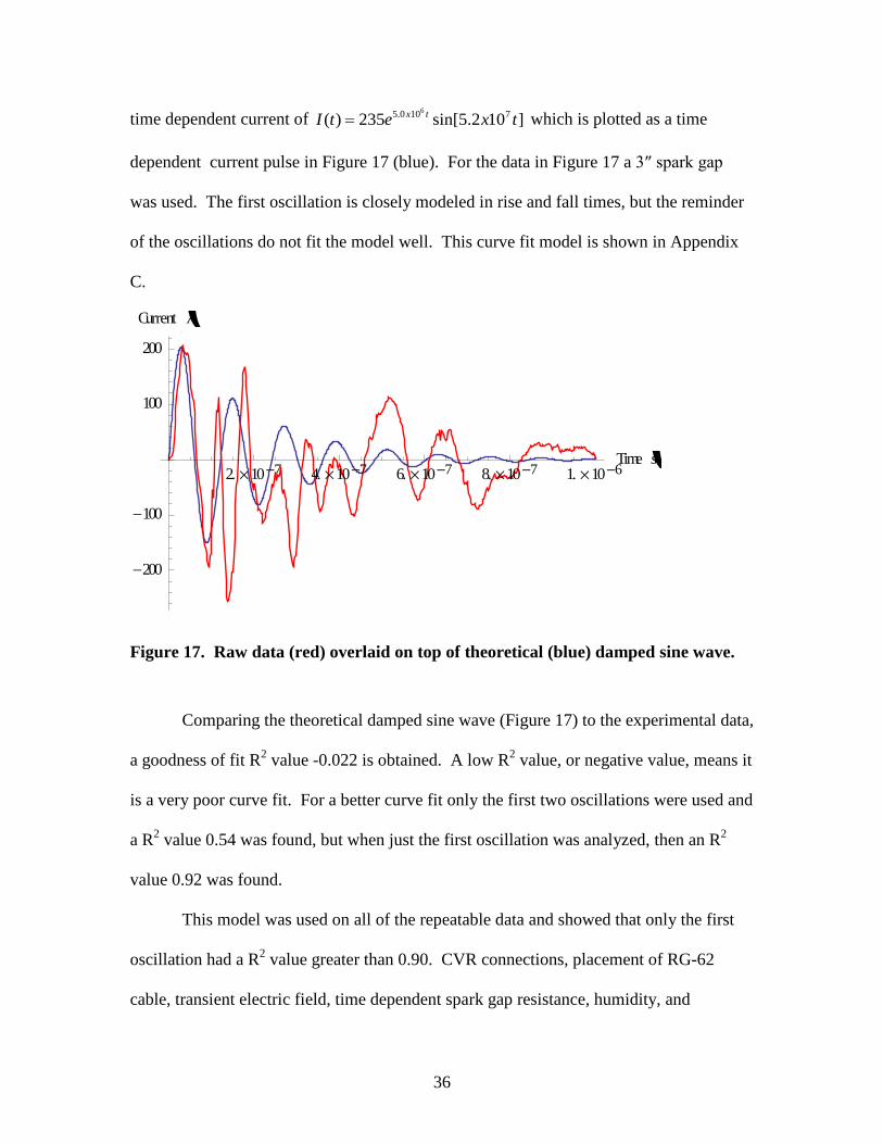
Figure 17. Raw data (red) overlaid on top of theoretical (blue) damped sine wave. ....... 36
Figure 18. Spark gap time-dependent current is damped after 6 oscillations. ................. 39
Figure 19. Spark gap time-dependent resistance decreases with time. ............................ 39
Figure 20. Scaled down spark gap current (red) compared to direct current (blue). ....... 40
xii
Figure 21. Two RG-62 cables and CVR equipment experimental setup. ......................... 44
Figure 22. Position A, B and C for CVR locations. ......................................................... 46
Figure 23. Experimental setup with CVR at position B. .................................................. 47
Figure 24. Experimental setup with CVR at position A. .................................................. 48
Figure 25. The Van de Graaff experimental setup used for all VDG experiments. ........ 51
Figure 26. Copper mesh clamps were used to connect the CVR. .................................... 53
Figure 27. All VDG system equipment was isolated from the concrete floor. ................ 54
Figure 28. VDG setup with RG-62 shielded coaxial cables. ............................................ 55
Figure 29. Current oscillations with CVR at position A. ................................................. 56
Figure 30. Current oscillations with CVR at position C. ................................................. 57
Figure 31. Plot of FFTs of full current pulses with the CVR at position A and C. ......... 57
Figure 32. FFT of the current pulse measured with CVR at position B. ......................... 59
Figure 33. Current pulse for the 3″ and 7″ spark gaps. .................................................... 60
Figure 34. Raw data (current as a function of time) for 3″ spark gap. ............................ 63
Figure 35. FFT for 3″ spark gap for experiment 1 and 2. ................................................ 64
Figure 36. Combined plot for experiments 1-4 for 3″ spark gap. .................................... 65
Figure 37. Curve fitted plot for the first oscillation for the data of experiment 1.. ......... 66
Figure 38. Direct drive current and frequency as a function of strike gap. ..................... 69
Figure 39. The best curve fit data was for experiment 3. ................................................ 71
Figure 40. Curve fit for a spark gap of 3″ along with the low and high current. ............. 72
Figure 41. Curve fit for a spark gap of 3″ along with standard deviations. ..................... 72
Figure 42. Current as a function of time measured with a resistor of 692 Ω. .................. 78
xiii
Figure 43. First oscillation of the current pulse measured with a resistor of 692 Ω. ....... 78
Figure 44. Charge density is greater on the roller than the inside of belt.. ....................... 85
Figure 45. High field strength ionizes the air gap to allow charge transport. .................. 85

xiv
List of Tables
Page
Table 1. Solutions to the underdamped second order linear differential equations. ......... 19
Table 2. Solutions to the overdamped model case are shown [14]. .................................. 20
Table 3. Solutions to the critically damped model case.................................................... 21
Table 4. Equipment used in current measurements of the VDG. ..................................... 26
Table 5. Properties of the coaxial cables used for all experiments [17]. .......................... 27
Table 6. Iterative algorithm to the time-dependent spark gap current. ............................ 38
Table 7. Impedance matching for a coaxial cable experiment. ......................................... 42
Table 8. Interference occurs when impedance is not matched using the RG-62 cables. .. 43
Table 9. Impedance bridging and shunt terminator experimental data. ........................... 44
Table 10. Two RG-62 cables and CVR experimental data. .............................................. 45
Table 11. Experimental data with CVR placed at position B. .......................................... 48
Table 12. Experimental data with CVR at position A. ..................................................... 49
Table 13. Humidity and temperature environments for the repeatable experiments. ...... 62
Table 14. FFT frequencies for measurements made at a spark gap of 3″. ....................... 67
Table 15. FFT frequencies for measurements made at a spark gap of 6″. ....................... 67
Table 16. FFT frequencies for measurements made at a spark gap of 7″. ....................... 67
Table 17. FFT frequencies for measurements made at a spark gap of 8″. ....................... 68
Table 18. Curve fit parameters for spark gap distance of 3″ ........................................... 70
Table 19. Goodness of fit statistics for spark gap distance of 3″. .................................... 70
Table 20. Curve fit parameters for spark gap of 6″ ......................................................... 73
Table 21. Goodness of fit statistics for spark gap of 6″. .................................................. 73

xv
Table 22. Curve fit parameters for spark gap of 7″. ........................................................ 73
Table 23. Goodness of fit statistics for spark gap of 7″. .................................................. 74
Table 24. Curve fit parameters for spark gap of 8″. ........................................................ 74
Table 25. Goodness of fit statistics for spark gap of 8″. .................................................. 74
Table 26. Summary of the maximum current. ................................................................. 75
Table 27. Summary of the average parameters for the first oscillations. ........................ 75
Table 28. Solution to the second-order linear differential equation. ................................ 88
Table 29. Voltage Load (VL) is higher when shunt terminators are used.. ...................... 89
Table 30. When CVR is placed in position A resonance is around 15 MHz. .................. 90
Table 31. Experiment data with CVR placed at the very back of the strike plate. .......... 91
1
ANALYSIS OF A VAN DE GRAAFF GENERATOR FOR EMP DIRECT CURRENT
SURVIVABILITY TESTING
CHAPTER 1
INTRODUCTION
1.1 Background
The rate of change of the electric and magnetic fields of an electromagnetic pulse
(EMP) event are a threat to electronic equipment. Equipment that performs critical, time-
urgent command, control, communications, computer, and intelligence (C4I) missions
must be hardened to operate through EMP events without damage or functional upsets.
Survivable C4I capabilities are essential to a credible military deterrent [1].
As with conventional weapons, nuclear weapon use is typically associated with
the blast, shock, and thermal effects. Additional effects, such as prompt radiation,
fallout, and EMP are less well understood and need additional study and experimental
analysis [2]. Therefore, the Van de Graaff (VDG) at the Air Force Research Laboratory
(AFRL) has been measured and analyzed for future use in EMP direct current
survivability testing and EMP educational benefit.
An abrupt pulse of electromagnetic radiation usually results from certain types of
high energy explosions, especially a nuclear explosion, or from a suddenly fluctuating
magnetic field. The resulting rapidly-changing electric and magnetic fields can couple
with electrical/electronic systems to produce damaging current and voltage surges.
The Department of Defense has established “Electromagnetic Environmental
Effects Requirements for Systems” as described in “MIL STD 464” [3]. In Section 5.5 of

2
MIL STD 464, it gives the parameters established to survive an EMP. The requirements
are: “The system shall meet its operational performance requirements after being
subjected to the EMP environment. If an EMP environment is not defined by the
procuring activity, Figure 1 shall be used. This requirement is not applicable unless
otherwise specified by the procuring activity. Compliance shall be verified by system,
subsystem, and equipment level experiments, analysis, or a combination thereof.” [3].
Figure 1. The MIL-STD-464 default model of a free-field EMP environment is shown. The EMP electric field is shown as a function of time [3]. This waveform conforms to the model equation, as shown in Equation (1):
/ /( ) ( ) ( )at bt t to oE t E k e e E k e eτ τ α β− − − −= − = − , (1)
3
where 50000oE = (V/m), 74 10aα τ= = × s-1, 86 10bβ τ= = × s-1, 1.3k = and
0.258=τ s [4].
1.2 Problem Statement and Purpose
The Van de Graaff (VDG) at the Air Force Research Laboratory (AFRL) at
Wright-Patterson AFB produces a transient electric field and an oscillating direct current
via discharge pulses. The first measured direct current oscillation of the VDG has a rise
time of 9 915 10 5 10 ( )s− −× ± × . This is within the validation range compared to the
military standard (MIL STD) for the free-field EMP environment that has a rise time of
92.5 10 ( )s−× , as shown in Figure 1. However, the fall time of the pulse produced from
the VDG is three times too short for validation testing. The VDG’s first direct current
oscillation was measured to be a sine wave with a fall time of 9 915 10 5 10 ( )s− −× ± × while
the MIL-STD-464 is an overdamped pulse with a fall time of 955 10 ( )s−× .
The VDG was found to produce an underdamped oscillating direct current pulse
that is damped with time. Therefore, the purpose of this thesis study was to determine if
the circuit resistance could be overdamped or critically damped; then the current pulse
would more closely model the MIL-STD-464 free-field EMP environment.
This research focused on measuring and evaluating the direct drive current
(current flowing through the strike plate) that is produced from the VDG. It was assumed
that the time dependence of the current must be the same as with the free form electric
field.
4
The goal of this research was to analyze the current pulse, and to explore whether
the system variables of spark gap resistance (which is spark gap length dependent),
equipment shielding, impedance matching, air breakdown saturation point, and circuit
series resistance could be changed or modified so as to change the underdamped
oscillatory current pulse into that of an overdamped system, thus meeting the free-field
MIL STD EMP environment parameters. This research relied on the establishment of a
reliable and repeatable method for obtaining current pulses from the VDG, to produce a
current that has the potential to be used for direct current EMP survivability testing.
1.3 Overview and General Approach The research of Dr. Charlesworth and Staniforth has modeled the VDG as an RLC
(resistor, inductor and capacitor) circuit, which has solutions analogous to the equations
for a damped harmonic oscillator [5]. Since the current flowing through the spark gap,
cannot be measured directly, this research was oriented on the direct current at the strike
plate. The oscillating current, which resulted from an electrostatic discharge of the VDG,
was examined in order to determine if the oscillations could be depressed via
overdamping of the RLC circuit. The purpose of which was to establish the degree to
which the circuit could be used for direct current EMP survivability testing.
To measure the direct current from the strike plate, a current viewing resistor
(CVR) was attached to the support cable of the strike plate. The CVR linearly converted
the current to a voltage signal which was measured on an oscilloscope. This time
dependence voltage pulse was analyzed for current amplitude and frequency. The

5
general layout of the experiment is shown in Figure 2, in which was measured the voltage
versus time. Current was then derived from a known value of the resistance of the CVR.
With the changing electric field that was generated by the VDG, magnetic fields
as well as conduction currents were produced. Equations that are used in evaluating
EMP are Ohm’s Law (Equation (2)), and two of Maxwell’s equations; Faraday’s Law
and Ampere’s Law (Equations (3) and (4), respectively).
Figure 2. Experiment concept plan for direct current measurement [6].
V IR= (2)
B xEt
∂− = ∇∂
(3)
0 0o oEJ xBt
µ ε µ ∂+ = ∇
∂
(4)

6
Ohm’s Law states that voltage (V), current (I) and resistance (R) are
interdependent. Faraday’s Law shows that changing magnetic fields ( B
) are generated
by electric fields ( E
), and Ampere’s Law says that conduction currents ( cJ
) are
generated by magnetic fields and/or changing electric fields.
For MIL-STD-464, the electromagnetic pulse fields, E
and B
, are modeled as
double exponential functions of time dependent fields from the product of a rise and a
decay function, as shown in Equation (6) that are developed from Equation (5) [3].
/ / / ( 1) / / /
( )( ) (1 )( ) ( ) ( )t at at a t at bt
o o o
B t (rising function)(decaying funciton)B t e B e B e e B e eτ τ τ τ τ τ− − − − + − −
=
= − = − = − (5)
In Equation (5), Bo, is the initial magnetic field (not the maximum); a is the discharging
coefficient, b is the charging coefficient where b = a+1, and τ is the time constant of the
charging source function. Since the magnetic and electric fields are related through the
constant, c (the speed of light), the free-field MIL-STD EMP generated electric field is
shown in Equation (6).
/ / / /( ) ( ) ( )at bt at bto oE t cB e e E e eτ τ τ τ− − − −= − = − (6)
Using Ohm’s law and a known resistance for the CVR, the current is determined through
scaling the measured voltage, as shown in Equation (7).
/ /( ) ( )at btoI t I e eτ τ− −= − (7)

7
CHAPTER 2
THEORY AND MODELING
2.1 Overview of Van de Graaff Operations
The Van de Graaff (VDG) is a large capacitor with an air-filled discharge gap.
The VDG transmits a current in a spark channel, following voltage breakdown of air
between the high voltage terminal (the VDG dome) and the strike plate. This is shown in
Figure 3. The VDG works on the principles of manipulating static electricity through the
triboelectric series.
The property known as static charge is generated by an accumulation of mobile
charged particles. Typically, matter is neutrally charged, meaning that the number of
electrons and protons are the same. If an atom has more electrons than protons, it is
negatively charged. If it has more protons than electrons, it is positively charged.
How strongly an atom holds on to its electrons determines its place in the
triboelectric series. If a material is more likely to give up electrons when in contact with
another material, it is more positive in the triboelectric series. If a material is more likely
to capture electrons when in contact with another material, it is more negative in the
triboelectric series.

8
Figure 3. AFRL’s Van de Graaff at Wright-Patterson, showing discharge to the strike plate.
The triboelectric series for common materials found in and around a VDG is
given [7]; positive triboelectric materials in the series are at the top, and negative ones are
at the bottom.
• Air (Very positive -Gives up electrons) • Human hands (usually too moist, though) • Human hair • Nylon • Aluminum (VDG bottom roller and dome head) • Steel (Neutral) • PVC (VDG structure) • Polyurethane (VDG drive belt) • Polytetrafluoroethylene (VDG top roller) • Teflon (Very negative - Captures electrons)
The relative position of substances in the triboelectric series indicates how they
will act when brought into contact. For example, polyurethane (VDG belt) brought next
to aluminum (VDG bottom roller) causes a charge separation because they are separated

9
in the triboelectric series; the bottom roller gives up electrons and becomes positively
charged while the belt captures electrons and becomes negatively charged, as shown in
Figure 4. Since the belt surface area is larger than the roller surface area, the surface
charge density will be greater on the roller than on the belt. The top roller made of
polytetrafluoroethylene has a charge transfer exactly opposite from the bottom roller.
Figure 4. A charge transfer takes place from the roller to the belt. Adapted from [8]. The VDG system is a charge pump that turns the dome head into a charged
capacitor. The VDG, as shown in Figure 3 is made up of a conveyor belt, made of
polyurethane, and a pair of rollers (polytetrafluoroethylene, the top roller, and aluminum,
the bottom roller) housed inside a structurally supported column made of PVC piping. A
metal comb, not visible in Figure 3, is placed adjacent to each roller, as shown in Figure
5. The metal combs do not physically touch the roller or the belt so that the charge
exchange is through a thin layer of air. A motor is used to drive the belt and move the
charge.
10
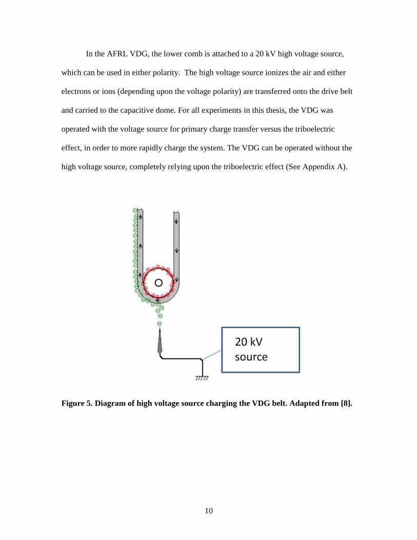
In the AFRL VDG, the lower comb is attached to a 20 kV high voltage source,
which can be used in either polarity. The high voltage source ionizes the air and either
electrons or ions (depending upon the voltage polarity) are transferred onto the drive belt
and carried to the capacitive dome. For all experiments in this thesis, the VDG was
operated with the voltage source for primary charge transfer versus the triboelectric
effect, in order to more rapidly charge the system. The VDG can be operated without the
high voltage source, completely relying upon the triboelectric effect (See Appendix A).
Figure 5. Diagram of high voltage source charging the VDG belt. Adapted from [8].
11
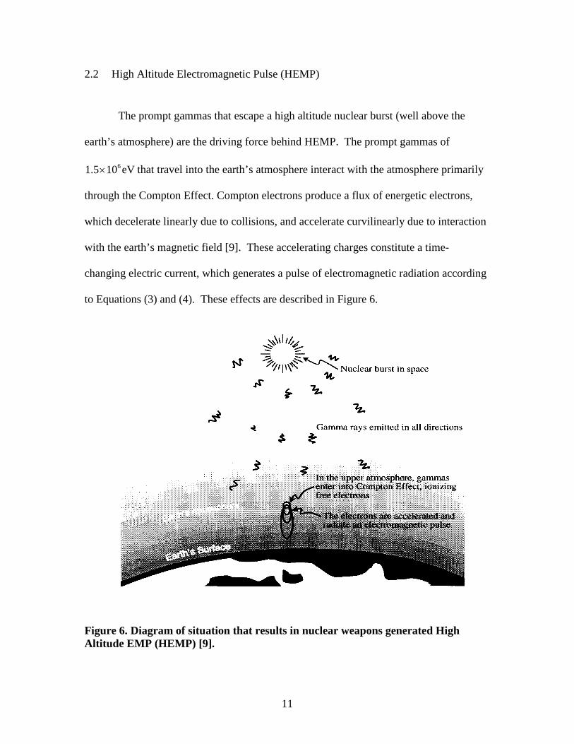
2.2 High Altitude Electromagnetic Pulse (HEMP) The prompt gammas that escape a high altitude nuclear burst (well above the
earth’s atmosphere) are the driving force behind HEMP. The prompt gammas of
61.5 10 eV× that travel into the earth’s atmosphere interact with the atmosphere primarily
through the Compton Effect. Compton electrons produce a flux of energetic electrons,
which decelerate linearly due to collisions, and accelerate curvilinearly due to interaction
with the earth’s magnetic field [9]. These accelerating charges constitute a time-
changing electric current, which generates a pulse of electromagnetic radiation according
to Equations (3) and (4). These effects are described in Figure 6.
Figure 6. Diagram of situation that results in nuclear weapons generated High Altitude EMP (HEMP) [9].

12
The rise time of this current is a mirror of the rise time of the gamma rays, which
in turn mirrors the weapon fission rise time. This fast rise time, faster than the rise time
of a lightning strike, gives the EMP pulse a unique high frequency component [9]. The
magnitude of an EMP voltage compared to a lighting strike, as well as electrostatic
discharge is shown in Figure 7. The purely empirical expression for the EMP pulse as
described by MIL STD 464 (see Equation (1)) is the difference between two
exponentials. Bridgman states, “The double exponential form poorly represents the
initial rise of the pulse and, as a result, misrepresents the high frequency content of the
pulse” [9]. Nevertheless, the double exponential is the presently approved Military
Standard pulse.
Figure 7. The magnitude of EMP, lighting and electrostatic discharge are compared [2].

13
2.3 Dielectric Breakdown of Air
Dielectric breakdown occurs when a charge buildup exceeds the electrical field
limit or dielectric strength of a material. In the breakdown of air, the negatively charged
electrons are pulled in one direction and the positively charged ions in the other. When
air molecules become ionized in a very high electric field, air then changes from an
insulator to a conductor.
Due to the very high electric field generated by the VDG, an oscillating current
(known as a strike) will then occur between the dome head and the strike plate. Strikes
occur because of the recombination of electrons in the air and ions on the strike plate. For
example, lightning occurs when there is a buildup of charge on the clouds and in the air.
This then produces the electric field between the clouds and the ground that exceeds the
dielectric strength of air. Ionized air is a good conductor, and provides a path whereby
charges can flow from clouds to ground, or in the VDG case, from the dome head to the
strike plate.
This phenomenon, which is called dielectric breakdown, occurs in air at an
electric field strength of about Emax = 63 10× V/m, at standard temperature and pressure.
The exact value varies with the shape and size of the electrodes, and increases with the
pressure of the air [7].
Personnel from AFRL provided the data on a single known point generated using
the VDG. On Feb 4, 2010 at 11:12 a.m. the breakdown potential was measured as
VBrkDwn 62.75 10× V at an electrode separation distance, d, of 91 cm [10]. The
temperature and relative humidity were 273.9 K and 73% [11].

14
The breakdown of air can be modeled as an underdamped RLC circuit that is
controlled by the dielectric breakdown of air. A simulated breakdown of air and its curve
fit is shown in Figure 8 [7]. The theoretical data shows a goodness of fit, or R2 value, of
95% to a damped sine wave described by the equation: ( ) sin( )tI t Ae tα ω−= . Goodness
of fit definitions are given in Appendix C.
Figure 8. Voltage as a function of time illustrating that the VDG is an underdamped RLC circuit that is controlled by the dielectric breakdown of air. Adapted from [7].
2.4 RLC (Resistor, Inductor, and Capacitor) Circuits
Staniforth and Charlesworth’s research showed that the VDG can be modeled
after an RLC circuit [5][12]. The VDG RLC circuit is shown in Figure 9. Using
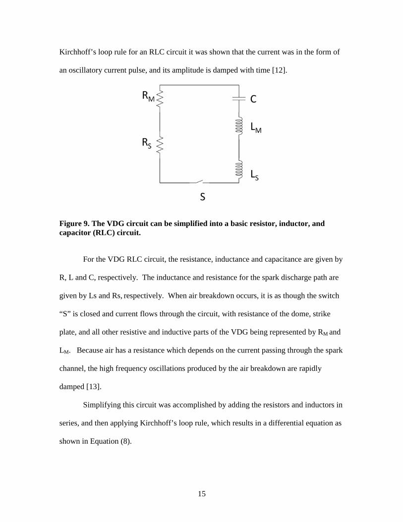
15
Kirchhoff’s loop rule for an RLC circuit it was shown that the current was in the form of
an oscillatory current pulse, and its amplitude is damped with time [12].
Figure 9. The VDG circuit can be simplified into a basic resistor, inductor, and capacitor (RLC) circuit.
For the VDG RLC circuit, the resistance, inductance and capacitance are given by
R, L and C, respectively. The inductance and resistance for the spark discharge path are
given by Ls and Rs, respectively. When air breakdown occurs, it is as though the switch
“S” is closed and current flows through the circuit, with resistance of the dome, strike
plate, and all other resistive and inductive parts of the VDG being represented by RM and
LM. Because air has a resistance which depends on the current passing through the spark
channel, the high frequency oscillations produced by the air breakdown are rapidly
damped [13].
Simplifying this circuit was accomplished by adding the resistors and inductors in
series, and then applying Kirchhoff’s loop rule, which results in a differential equation as
shown in Equation (8).

16
0dI QL IRdt C
+ + = (8)
Replacing I with /dQ dt in equation (8), a second-order linear differential equation with
constant coefficients is obtained as shown in Equation (9).
2
2
1 0d Q dQL R Qdt dt C
+ + = (9)
Equations (8) and Equation (9) are analogous to the mass on a spring equation for a
damped harmonic oscillator, as shown in Equation (10).
2
2 0d dxm b kxdt d
xt
+ + = (10)
In the oscillation of a mass on a spring, the damping constant b leads to a
dissipation of energy. In an RLC circuit, the resistance R is analogous to the damping
constant b of the spring and leads to a dissipation of energy.
If the resistance is small, the current oscillates with angular frequency that is very
nearly equal to 𝜔0 = 1√𝐿𝐶� . This frequency is called the natural frequency or
resonance frequency of the circuit.
Equation (8) was shown qualitatively from energy considerations. Multiplying
each term in equation (8) by the current, I, leads to Equation (11).
2 0dI QLI I R Idt C
+ + = (11)
The magnetic energy in the inductor is given by 𝑈𝑚 = 12
𝐿𝐼2 + 𝐶 . The derivative of the

17
magnetic energy leads to Equation (12).
21( )
2d LI dILI
dt dt= (12)
Therefore, LI dI/dt, the first term in Equation (11), is the time rate of magnetic energy
stored in the circuit. If LI dI/dt is positive, it equals the rate at which electrical potential
energy is transformed into magnetic energy. If LI dI/dt is negative, it equals the rate at
which magnetic energy is transformed back into electrical potential energy. Note that
whether LI dI/dt is positive or negative depends on whether I and dI/dt have the same
sign or different signs. The second term in equation (11) is I2 R, the rate at which
electrical potential energy is dissipated in the resistor. This term is never negative.
The electric energy stored in the capacitor is shown in Equation (13).
21 1
2 2e cQU QVC
= = (13)
The derivative of Equation (13) results in Equation (14).
21( )2
Qd Q dQ QC Idt C dt C
= = (14)
IQ/C is the third term in Equation (11), and represents the rate of change of electric
energy stored in the capacitor, which may be positive or negative. For the RLC circuit
the sum of the electric and magnetic energies is not constant because energy is

18
continually dissipated in the resistor, thereby damping the oscillations. The solutions to
the second order linear differential equation are shown in Appendix A.
2.4.1 Modeled RLC Circuits
MIL-STD-464 requires a single electromagnetic pulse for testing, while the VDG
produces an oscillating sinusoidal current pulse. To better simulate the required pulse for
MIL-STD-464, the RLC circuit of the VDG needs to be over or critically damped. The
RLC circuit is the primary model for most high voltage and pulsed power discharge
circuits. To illustrate this point an example of a series RLC circuit, as described in Figure
9, will be taken from an underdamped circuit to an overdamped then critical damped
system [14]. This RLC circuit becomes a completed circuit when the switch (air
breakdown between the VDG dome and the strike plate occurs) is closed. For this
simulation the total inductance of the circuit is 610− H, the total capacitance is 610− F, the
initial voltage on the capacitor is 10 V and the total resistance is varied between 0.2, 20
and 2 Ω to show the difference between the under, over, and critically damped situations.
2.4.1.1 Underdamped RLC circuit when 𝑅2 < 4𝐿𝐶�
The current with a known capacitance, inductance and resistance were graphed.
Figure 10 shows graphs of the under, over and critically damped cases when the
resistance is varied between 0.2, 20 and 2 Ω. The under damped case is shown when the
resistance is an order of magnitude (10x) less than the value required for a critically
damped circuit. In Figure 10 the upper graph shows the current with a 0.2 Ω resistor.

19
The circuit current reaches its peak value at ~ 0/ 2t π ω= . The solutions to the
underdamped model case are shown in Table 1.
Figure 10. Current as a function of time is graphed for an under, over and critical damped RLC series circuit.
Table 1. Solutions to the underdamped second order linear differential equations for an RLC circuit [14].
20
1 ( )2R
LC Lω = − Omega
L is the circuit inductance (H) C is the circuit capacitance (F) R is the circuit resistance (Ω )
( )0 20
0
( ) ( ) sin( )R tLVi t e t
Lω
ω
−
= Current V0 is the initial voltage on the capacitance (V)
0( )
0
0
( )R
LPeak
VI eL
ω
ω
−
= Peak Current Same as above
0 10 20 30 40 50 60 70 80-10
0
10
Cur
rent
, I(t)
(A) (a) Underdamped
0 10 20 30 40 50 60 70 800
0.5
Cur
rent
, I(t)
(A) (b) Overdamped
0 10 20 30 40 50 60 70 800
2
4
Cur
rent
, I(t)
(A) (c) Critically Damped
Time (µ s)

20
2.4.1.2 Over damped RLC circuit when 𝑅2 > 4𝐿𝐶�
The circuit schematic for the overdamped RLC circuit is shown in Figure 9. The
resistance is an order of magnitude (10x) larger than required for a critically damped
circuit with a resistance of 20 Ω.
The results of the overdamped circuit are shown in the middle graph of Figure 10.
To drive this overdamped model the load resistor has a 20 Ω value. Once the switch
closes the voltage on the load resistor rises to match the capacitor voltage and the current
damps with time. The solutions to the underdamped circuit case are shown in Table 2.
Table 2. Solutions to the overdamped model case are shown [14].
20 ( )
2R LL LC
ω = − Omega L is the circuit inductance (H) C is the circuit capacitance (F) R is the circuit resistance (Ω )
( )0 20
0
( ) ( ) sinh( )R tLVi t e t
Lω
ω
−
=
Current V0 is the initial voltage on the
capacitor (V)
2.4.1.3 Critically Damped RLC circuits when 𝑅2 = 4𝐿𝐶�
The circuit schematic for the critically damped model case is shown Figure 9. In
this critical damped model, the resistance is exactly equal to the value required for a
critically damped circuit, or 𝑅2 = 4𝐿𝐶� (with R= 2 Ω). The results of the circuit model
are shown in the bottom graph of Figure 10, and the solutions to the critically damped
model case are shown in Table 3. In Figure 10 the circuit current reaches its peak value

21
at t=2L/R. This circuit is often desirable (if possible) with high voltage energy storage
capacitors, since voltage reversals can frequently decrease the lifetime of the capacitor.
The modeled cases of the under, over and critically damped RLC circuit show that
to meet MIL-STD-464 standard the circuit needs to be configured with R, L, and C so
that the circuit is over or critically damped.
Table 3. Solutions to the critically damped model case.
( )0 2( ) ( )R tLV ti t e
L
−
= Current
V0 is the initial voltage on the capacitor (V) L is the circuit inductance (H) R is the circuit resistance (Ω )
0 02 0.736PeakV VI
eR R= ≈ Peak Current Same as above
2.4.2 Time dependence of the Spark Gap Resistance In the simple RLC model of Section 2.4.1, R, L and C were constants. However,
in the VDG the spark gap resistance (Rs) is time dependent. Staniforth and Charlesworth
measured the spark gap resistance and showed that it depends on the current passing
through the spark gap, which is time dependent for the VDG [12]. It was found that the
variation of resistance for all gases through the spark gap can be approximated by using
Equation (15).
( )4 1/3
23
0
7.0 10
( )s t
xR ti t dt
ρ−
=∫
(15)
In Equation (15), ρ is the gas density (kg/m3) before breakdown, ( )i t is the time
dependent spark channel current (A), and is the spark gap length (m). It was also
22
shown that the inductance (L) of the spark gap is independent of the gas pressure,
damping increases with the terminal strike plate spacing, and ( )sR t rapidly decreases
with time [5]. The value of ( )sR t is obtained at a particular time using Equation (15).
In the VDG analysis and research, the equipment to measure the spark gap current
was not available, and manipulating the gas density in an open room was outside the
scope. Therefore, the primary experiment to manipulate ( )sR t was done by varying the
spark gap length.
2.4.3 VDG Circuit Inductance and Capacitance
Energy storage via inductance occurs when current passes through a
magnetic field. The inductance is related to the current and magnetic flux as ∅𝑚 = 𝐿𝐼.
In principle, the inductance of any coil or circuit can be calculated by assuming a current,
I, and then calculating the magnetic field at every point on a surface bound by the coil or
circuit, and then calculating the magnetic flux, and finally using 𝐿 = ∅𝑚/𝐼. Since the
current in the spark gap is time-dependent, the induction is also time-dependent.
Charlesworth and Staniforth measured the current flowing in the spark gap and
found that the channel inductance is approximated by 1.4 nH/mm for both small (1.5
MV) and large (10 MV) VDGs [5][12]. Using this assumption and a spark gap distance
of 6″, the induction of the VDG was found to be 9213 10−× H.
The capacitance for the VDG was calculated to be 114.5 10−× F [6], with the
assumption that the VDG capacitance is calculated in three parts that are added together.

23
The top of the VDG dome is a capacitor that is made of a hollow aluminum hemisphere.
The capacitance of a sphere, Csphere, is given in Equation (16).
spheresphere o rC = 4 Rπ ε ε (16)
In Equation (16), RSphere is the spherical radius of the VDG dome and εr is the dielectric
constant. The hemisphere is set over the bottom half of the dome, which is a hollow,
horizontally aluminum oriented toroid. An empirical equation for the capacitance of a
toroid, Ctoriod, in pF, is shown in Equation (17) [15].
(0.37 0.23 )toroid r Major MinorC D Dε= + (17)
Therefore, the total capacitance of the VDG dome was found using Equation (18).
2
sphere toroiddome
C CC
+= (18)
The final capacitance component is the air volume capacitance, CAirVolume. The air
volume is that of the space between the two electrodes. This component is a function of
the spark gap distance and is also calculated by changing Equation (16) to read:
airAirVolume o rC = 4 Rπ ε ε . Therefore, CTotal is spark gap dependent. The capacitance of the
VDG system is found by CTotal = Cdome + CAirVolume.
2.5 Current Measurements via a Current Viewing Resistor (CVR)
24
An SDN-414-05 model, current viewing resistor (CVR) with a known resistance
of R=0.02651 Ω was used to measure the time dependent current for electrostatic
discharges from the VDG. This CVR model has a maximum band pass frequency of
92 10× Hz, a minimum rise time of 101.8 10−× s, and a maximum energy of 2 joules [16],
which was sufficient for all measurements in this thesis.
A sample energy calculation using typical values is shown in Equation (19) [6].
Using a maximum current of 450 (A) and a full width half maximum (FWHM) time of
72.91 10−× s, the CVR is well within its design limits.
2 -3
-7
Energy (J), E=i Rt=1.56×10Current (A), i=450Resistance (ohms), R=0.02651time (s) (FWHM), t=2.91×10
(19)
The use of the current to verify the time dependence of the spark gap electric field
is problematic as the current through the CVR does not fully measure the spark gap
current (and thus the electric field time dependence) for the spark gap. There are multiple
measurement options for the current flow and energy storage in the circuit as noted in
Chapter 3. To reduce these issues, impedance matching, shielding of cable and
equipment, as well as placement of the CVR were analyzed.
25
2.6 Impedance Matching Measurements The equipment used in this thesis is listed in Table 4. The cables, voltage source,
oscilloscope, VDG and strike plate all have characteristic impedances. Pulse
transmissions through coaxial cables are divided into two cases: 1) low-frequency, or
slow pulses and 2) high-frequency, or fast pulses. The VDG generates electromagnetic
pulses with frequency components into the MHz range, which are (by definition) fast
pulses. A fast pulse has a rise time that is shorter than the cable transit time. For fast
pulses, the characteristic impedance of the cable becomes important, because it describes
the ability of the pulse to transit the cable unimpeded. This characteristic impedance
depends on the dielectric material and diameter of the inner conductor and the outer
shield of the cable; but is independent of the cable length, as shown in Figure 11. The
properties of the coaxial cables used in this research are shown in Table 5.

26
Table 4. Equipment used in current measurements of the VDG.
Van de Graaff Generator (VDG)
Built at AFRL. The Arc of the Dome is ~ 7’ above the floor.
Oscilloscope Tektronix TDS 5104B
Current Viewing Resistor T & M Research Products. SERIES SDN-414-0.025
Power Supply (Generator) No Manufacturer or Model Listed ID No.: C845588 S.N. N225035-01CJ090204
Power Switch General Electric Fuji AF-300 Mini
Model NEMA 1XCID S.N.: 7BZ471A0008
Cable RG 58C/U with a Characteristic Impedance of 50 Ω and Signal Propagation of 0.659 × speed of light
RG62A/U with a Characteristic Impedance of 93 Ω and Signal Propagation of 0.840 × speed of light
Connectors BNC and commercial alligator clips
Shunt Terminators 50 and 100 Ω
Barometer Nimbus Digital Barometer SN B6C8F2N01
Signal Generator Agilent 33220A – 20MHz Function
Figure 11. Construction of a standard coaxial cable. Adapted from [17].

27
Table 5. Properties of the coaxial cables used for all experiments [17]. Cable
Type
Insulating
Material
Cable
Diameter
(cm)
Characteristic
Impedance
(Ω )
Signal
Propagation
(fraction of
3x10⁸ m/s)
HV
Rating
(V)
Cable
Capacitance
(pF/m)
Signal
Attenuation per
Meter
MHz dB
RG-
58C/U
Polyethylene 0.50 50 0.659 1900 100.1 100
400
0.174
0.413
RG-
62/U
Polyethylene 0.61 93 0.840 750 44.3 100
400
0.102
0.207
Impedance is considered matched when the voltage source, VS, equals the voltage
load, VL, as shown in the schematic of Figure 12. When impedance is matched,
maximum power is transferred from source to load, and reflections along the transfer
cable are minimized.
Figure 12. Circuit diagram for impedance matching. Adapted from [17].
In this circuit the impedance, ,T S LZ Z Z= + represents the opposition to the flow
of energy from a source. For a constant current source (i.e. DC) the impedance is simply
the circuit resistance, but for varying signals (i.e. AC) like those produced by the VDG,
the impedance is a function of frequency. Impedance is represented as a complex value;

28
the real part represents the resistance, R, while the complex part represents the reactance,
X, or the time dependent part. These relationships are shown in Equation (20) with j
being the imaginary number.
1
Z R jX
j
= +
= − (20)
Both capacitive reactance XC and inductive reactance XL contribute to the total
reactance, as shown in Equation (21); both are dependent on the frequency of the signal
or system.
1 12
2
C L
C
L
X X X
XC fC
X L fLω πω π
= +
− −= =
= =
(21)
If X is greater than zero, the reactance is said to be inductive. If X is less than zero, the
reactance is said to be capacitive, and if X equals zero, then the impedance is all resistive.
This happens when the magnitude of XC equals the magnitude of XL and happens at
resonant frequency. At resonant frequency, maximum power is delivered from the
current source to the current load.
2.7 Resonant Frequency Resonance of a circuit involving capacitors and inductors occurs because the
collapsing magnetic field of the inductor generates an electric current that charges the
capacitor, and then the discharging capacitor provides an electric current that builds the

29
magnetic field in the inductor. This process is repeated continuously. An analogy is a
mechanical pendulum.
Resonant frequency is reached when 1o LC
ω = , as shown in Equation (22). At
resonant frequency maximum power is obtained in the system, and therefore peak current
is reached. Resonance is approached as reactance approaches zero and impedance is
minimized. Experimentally, resonance is measured as voltage and current reach their
peak values.
When the CVR was placed in line on the equipment experiments, the resonant
frequency of the VDG system was experimentally found to be near 15 MHz. The
equipment resonance experiment is described in Appendix B.
20
1 1 1C LX X
LC LC LCω ω ωω
=
= → = → = (22)
2.8 Skin Effect in metallic conductors The skin effect is the tendency of an AC current to become distributed within a
conductor such that the current density is largest near the surface of the conductor, and
decreases toward the center. The electric current flows mainly at the skin of the
conductor, between the outer surface and a distance called the skin depth. The skin effect
causes the effective resistance of a conductor to increase at higher frequencies, where the
skin depth is smaller, thus reducing the effective cross-section of the conductor. The skin
effect is due to opposing eddy currents (Iw), induced by the changing magnetic field
resulting from an AC current. At high frequencies, the skin depth becomes much smaller,
30
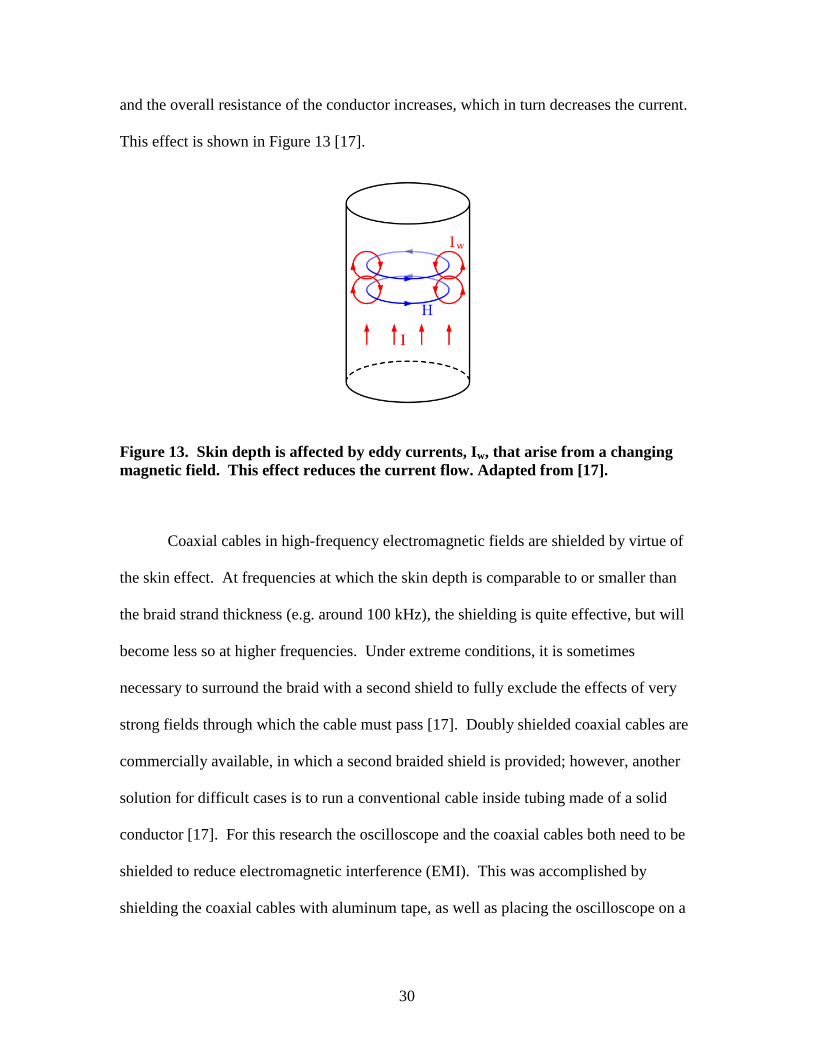
and the overall resistance of the conductor increases, which in turn decreases the current.
This effect is shown in Figure 13 [17].
Figure 13. Skin depth is affected by eddy currents, Iw, that arise from a changing magnetic field. This effect reduces the current flow. Adapted from [17]. Coaxial cables in high-frequency electromagnetic fields are shielded by virtue of
the skin effect. At frequencies at which the skin depth is comparable to or smaller than
the braid strand thickness (e.g. around 100 kHz), the shielding is quite effective, but will
become less so at higher frequencies. Under extreme conditions, it is sometimes
necessary to surround the braid with a second shield to fully exclude the effects of very
strong fields through which the cable must pass [17]. Doubly shielded coaxial cables are
commercially available, in which a second braided shield is provided; however, another
solution for difficult cases is to run a conventional cable inside tubing made of a solid
conductor [17]. For this research the oscilloscope and the coaxial cables both need to be
shielded to reduce electromagnetic interference (EMI). This was accomplished by
shielding the coaxial cables with aluminum tape, as well as placing the oscilloscope on a

31
table (~ 3′ from the floor) and 4′ outside of the VDG room; also taking advantage of the
field reduction with distance and shielding provided by the room walls.
2.9 Constructive and Destructive Reflections
Reflections in the coaxial cable are caused by abrupt changes in the electrical
properties of the media through which the signal is propagated. This is commonly
referred to as impedance mismatch. If the cable is connected to an electronic component,
then the termination resistance is effectively just the input impedance of that component
(i.e. oscilloscope). If the entire system is impedance matched then there will be no
reflections and the load signal will not be diminished or enhanced due to constructive or
destructive interference.
To minimize reflections, impedance matching is achieved by making the load
impedance, ZL, equal to the source impedance, ZS. Ideally, the source and load
impedances should be purely resistive. The transmission line (example RG-58C/U)
connecting the source and load together must also have the same impedance: Zload = Zline
= Zsource, where Zline is the characteristic impedance of the transmission line. The
transmission line characteristic impedance should also ideally be purely resistive. Cable
makers try to get as close to this ideal as possible, and transmission lines are often
assumed to have purely resistive characteristic impedances. This technique is known as
reflection-less matching.

32
2.10 Effect of bridging and shunt terminators on circuit performance Impedance bridging is defined when the load impedance, ZL, is much larger than
the source impedance, ZS (i.e. ZS<<ZL). Maximizing the load impedance serves to both
minimize the current drawn by the load and to maximize the voltage signal across the
load. The source impedance of the circuit is the combined internal resistance. Applying
Kirchhoff’s loop rule to Figure 12, Equation (23) resulted [17]. Equation (23) shows that
if ZS is low compared to ZL, then s LV V≈ , and essentially all of the signal voltage is
transmitted to the load (i.e. oscilloscope).
( )
( )
S S L
L L
L
L
S LS L
L
LL S
S L
V iZ iZV iZ
ViZ
Z ZV VZZV V
Z Z
= +
=
=
+=
=+
(23)
To further reduce ZS and enhance the bridging method, a resistor-to-ground
(called a shunt terminator) was inserted parallel to the input of the oscilloscope so that the
effective termination is the parallel combination of the source impedance and the shunt
terminator resistance; effectively reducing the source impedance. As an example, a 100 Ω
terminator added in parallel with an RG-62/U coaxial cable with a characteristic
impedance of 93 Ω results in a total impedance of 48.18 Ω, as shown in Equation (24).
33
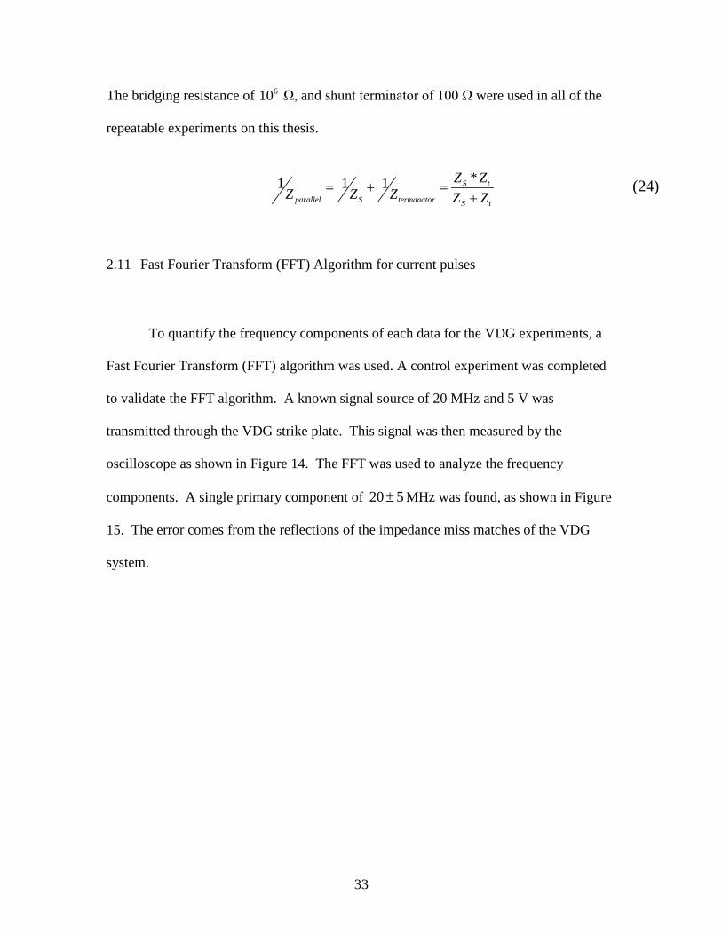
The bridging resistance of 610 Ω, and shunt terminator of 100 Ω were used in all of the
repeatable experiments on this thesis.
*1 1 1 S t
parallel S termanator S t
Z ZZ Z Z Z Z
= + =+
(24)
2.11 Fast Fourier Transform (FFT) Algorithm for current pulses
To quantify the frequency components of each data for the VDG experiments, a
Fast Fourier Transform (FFT) algorithm was used. A control experiment was completed
to validate the FFT algorithm. A known signal source of 20 MHz and 5 V was
transmitted through the VDG strike plate. This signal was then measured by the
oscilloscope as shown in Figure 14. The FFT was used to analyze the frequency
components. A single primary component of 20 5± MHz was found, as shown in Figure
15. The error comes from the reflections of the impedance miss matches of the VDG
system.

34
Figure 14. Known signal source of 20 MHz and 5 volts.
Figure 15. FFT for a 20 MHz 5 volt source.
-4 -2 0 2 4 6 8 10 12
x 10-8
-2
-1.5
-1
-0.5
0
0.5
1
1.5
2
Frequency (Hz)
Vol
tage
(V)
0 10 20 30 40 50 60 70 80 90 1000
1
2
3
4
5
6
7
8
9
10x 10
9
Frequency (MHz)
Four
ier T
rans
form
(Arb
. Uni
ts)

35
2.12 VDG Measurements compared to current Models
2.12.1 Experimental comparison to the Damped Sine Wave model
All initial experimental current pulses from the VDG represented an underdamped
circuit. To solve for the damping coefficient, Equation (25) was used [12].
12
1 2 1 212
2 1 2 1
( ) sinln ln ln( / )
2
ti t Ae tI I I It t t t
f
α ω
α
ω π
−=−
≈ =− −
=
(25)
The current magnitudes I1 and I2 were determined together with the associated times t1
and t2, and the assumption was made that during the time interval t2-t1, the damping
coefficient 12α was constant so that the discharge current, i, could be expressed by i(t).
Figure 16. Typical discharge current pulse produced from a VDG (smoothed) [12].
Using an amplitude of 235 (A) and a frequency of 8.3 MHz, the damping
coefficient was determined numerically using a least squares fitting routine, resulting in a
36
time dependent current of 65.0 10 7( ) 23 5.25 0sin[ ]1x tI xt e t= which is plotted as a time
dependent current pulse in Figure 17 (blue). For the data in Figure 17 a 3″ spark gap
was used. The first oscillation is closely modeled in rise and fall times, but the reminder
of the oscillations do not fit the model well. This curve fit model is shown in Appendix
C.
Figure 17. Raw data (red) overlaid on top of theoretical (blue) damped sine wave.
Comparing the theoretical damped sine wave (Figure 17) to the experimental data,
a goodness of fit R2 value -0.022 is obtained. A low R2 value, or negative value, means it
is a very poor curve fit. For a better curve fit only the first two oscillations were used and
a R2 value 0.54 was found, but when just the first oscillation was analyzed, then an R2
value 0.92 was found.
This model was used on all of the repeatable data and showed that only the first
oscillation had a R2 value greater than 0.90. CVR connections, placement of RG-62
cable, transient electric field, time dependent spark gap resistance, humidity, and
2. 107 4. 107 6. 107 8. 107 1. 106Times
200
100
100
200
CurrentA

37
temperature were all assumed to cause differences from the simple theoretical model.
Therefore it was found that only an analysis of the first oscillation is repeatable and the
modeling parameters of a single sine wave are useful.
2.12.2 Spark Gap Model In an ideal RLC circuit R, L, and C are held constant but in the VDG Rs and L are
time dependant and C is spark gap length dependent. Therefore, a model was developed
to explore the effects of the time dependent current in the spark gap. The model solves
the RLC circuit with a time dependent resistance based upon Charlesworth and
Staniforth’s equation for spark gap resistance, shown in Equation (15) [12], and the
underdamped time dependent current, shown in Section 2.4.1.1 Table 1.
( )0 20
0
( ) ( ) sin( )R tLVi t e t
Lω
ω
−
=
20
1 ( )2R
LC Lω = − )
( )4 1/3
23
0
7.0 10
( )s t
xR ti t dt
ρ−
=∫
The model methodology is shown in Table 6. Rs is the spark gap resistance, L is
inductance, C is capacitance, ωo is angular frequency, and V0 is initial voltage. The flow
of the algorithm is from top left to top right, then down one row for the next iterative
step. The model is shown in Appendix C.

38
At time zero, 2/3
0( )
ti t dt∫ was assumed to be 10-9 (A) so that a singularity would
not exist when solving for the first step of R. For a spark gap maximum current of 2600
(A), as shown in Figure 25, the error introduced is small.
Table 6. Iterative algorithm to the time-dependent spark gap current. Start here → Then ↓
2/3
0( )
ti t dt∫ Rs wo i(t)
At t=0 910− 4 1/3
2/3
0
7 10
( )tx l
i t dt
ρ−
∫ 21 ( )
2R
LC L− 0 2
0
sinRtL
oV e t
Lω
ω
−
t= 111 10−×
(step 1)
2/3
0( )
ti t dt∫ +
i(t)2/3*dt
4 1/3
2/3
0
7 10
( )tx l
i t dt
ρ−
∫ 21 ( )
2R
LC L− 0 2
0
sinRtL
oV e t
Lω
ω
−
t= 112 10−×
(step 2)
same same same Same
... ... ... ... ...
Until t=tmax ... ... ... ...
Using Charlesworth and Staniforth’s known values for a 10 MV VDG, L =
370nH and C = 200pF [12], a spark gap of 3″, and air density of 1.225 kg/m3, the time-
dependent current was found as shown in Figure 18. To compare to known values, the
spark gap resistance is also plotted, as shown in Figure 19; these values correspond well
with the data in [12].

39
Figure 18. Spark gap time-dependent current is damped after 6 oscillations.
Figure 19. Spark gap time-dependent resistance decreases with time.
0 0.1 0.2 0.3 0.4 0.5 0.6 0.7 0.8 0.9 1
x 10-6
-2000
-1500
-1000
-500
0
500
1000
1500
2000
2500
3000
Time (s)
Spa
rk G
ap C
urre
nt (A
)
10-2
10-1
100
101
102
103
101
102
103
104
105
Time (ns)
Spa
rk R
esis
tanc
e (o
hms)

40
To compare the spark gap time-dependent current to experimental data, it had to
be scaled to the measured current. The data for a spark gap of 3″ is plotted against the
scaled version of the modeled spark gap current, as shown in Figure 20. The modeled
current is fully damped at 60.3 10 ( ),s−× while the experimental data is damped after
610 ( )s− .
Although an RLC circuit model provides initial insight into the expected current
waveform, in this research the more physical results of adding a time dependent spark
gap resistance were explored. The resultant model verifies that the time dependent
current is oscillatory and damped with time. When comparing the modeled spark gap
current to the direct current, even the first oscillation appears with reflective interference,
as the model’s first oscillation’s primary frequency component is 15 MHz as compared to
the experimental data of 8 MHz as determined from Fourier analysis.
Figure 20. Scaled down spark gap current (red) compared to direct current (blue) for a 3″ spark gap, and the CVR placed at position A on the support cable, as shown on Figure 22.
0 0.2 0.4 0.6 0.8 1 1.2
x 10-6
-300
-200
-100
0
100
200
300
Time (s)
Cur
rent
(A)

41
CHAPTER 3
VDG EXPERIMENTS
3.1 Equipment Confidence Experiments
3.1.1 Introduction Equipment confidence experiments were conducted before subjecting the
oscilloscope, coaxial cables (which were shielded with aluminum tape), and BNC
connectors to the high currents generated from the VDG and the EMI (Electromagnetic
Interference) from the transient electromagnetic pulse during an electrostatic discharge.
All equipment confidence experiments were conducted with a signal source generator
instead of the VDG, in order to gain confidence in the measuring equipment, and
methodologies used.
A signal source generator was used to send a sinusoidal wave of fixed amplitude
through the aluminum foil-shielded coaxial cables (RG-62/U and/or RG-58 C/U) to the
strike plate, and then either into the CVR or directly into another shielded coaxial cable to
the oscilloscope. The purpose was to verify that the wave was not distorted, and that the
oscilloscope was reading the voltage signal correctly.
3.1.2 Response to Reflection-less (Impedance) Matching
Reflection-less matching was used as the baseline equipment confidence
experiment. The signal source had an impedance of 50 Ω, the RG-58C/U transmission
cable had a characteristic impedance of 50 Ω, and the oscilloscope was set to a 50 Ω
termination. If impedance can be matched correctly then maximum power is

42
transmitted, and VS =VL. The voltage drops shown in Table 7 are from the skin effect at
frequencies above 1 MHz, as well as characteristic cable impedance. This experiment
demonstrated the skin effect theory. The signal source was connected directly to the
oscilloscope through a coaxial cable; the data is shown in Table 7.
Table 7. Impedance matching for a coaxial cable experiment.
Signal Source
(50 Ω impedance)
Oscilloscope
(Terminated at 50 Ω) with
RG-58C/U (50 Ω) cable of 15ft length
Frequency Voltage Frequency Voltage
1 MHz 1 V 1 MHz 1 V
1 MHz 5 V 1 MHz 5 V
1 MHz 10 V 1 MHz 10 V
1 MHz 5 V 1 MHz 5 V
10 MHz 5 V 10 MHz 4.92 V 15 MHz 5 V 15 MHz 4.92 V
20 MHz 5 V 20 MHz 4.88 V
3.1.3 Response to Reflections (Impedance miss-matched) The experiment was repeated, but with RG-62/U coaxial cables of different
lengths. These cables have a characteristic impedance of 93 Ω, and would not be
impedance-matched with either the signal source or the signal load of the oscilloscope
since the source and load impedances were still 50 Ω. This had the effect of producing
destructive interference and the oscilloscope indicated that the peak voltage was reduced
compared to the reflection-less experiment; compare Table 7 to Table 8.

43
Table 8. Interference occurs when impedance is not matched using the RG-62 cables.
Signal Source
(50 Ω impedance)
Oscilloscope
(Terminated at 50 Ω) with RG-
62 (93 Ω) cable of 3ft length
Oscilloscope
(Terminated at 50 Ω) with RG-
62 (93 Ω) cable of 30ft length
Frequency Voltage Frequency Voltage Frequency Voltage
1 MHz 1 V 1 MHz 0.98 mV 1 MHz 0.96 mV
1 MHz 5 V 1 MHz 5 V 1 MHz 4.88 V
1 MHz 10 V 1 MHz 9.98 V 1 MHz 9.80 V
1 MHz 5 V 1 MHz 5 V 1 MHz 4.88 V
10 MHz 5 V 10 MHz 4.98 V 10 MHz 4.32 V
15 MHz 5 V 15 MHz 4.94 V 15 MHz 4.84 V
20 MHz 5 V 20 MHz 4.88 V 20 MHz 4.10 V
At high frequencies, the total reactance of Equation (21) was increased thereby
decreasing VL. The increase of the VL for the 30′ cable (i.e. 4.32 V up to 4.84 V) from the
10 MHz to 15 MHz is likely from resonance constructive interference as shown in
Appendix B. The cable lengths also affected the measurements as cable capacitance is
length dependent, as shown in Table 5. The added impedance caused by the increase of
cable length decreases VL from the 3 to the 30′ cable length for all frequencies measured.
3.1.4 Response to the bridging and shunt terminator
The bridging method, having the load impedance ZL much larger than the source
impedance ZS (i.e. (ZS<<ZL) for maximizing the voltage signal across the load was
investigated. The oscilloscope was terminated at 610 Ω and a shunt terminator of 50 Ω
was added in parallel, the results are shown in Table 9. This method resulted in a clean
44
waveform and was used for all follow on experiments. For impedance matching a 50 Ω
shunt terminator should be used on the RG-58 cable experiments and a 100 Ω shunt
terminator for the RG-62 cable experiments; as these shunts match and closely match the
respective characteristic cable impedances, as shown in Table 5.
Table 9. Impedance bridging and shunt terminator experimental data.
Signal Source
(50 Ω impedance)
Coaxial Cable RG-58C/U (15ft)
Oscilloscope terminated at 610 Ω
and a shunt terminator of 50 Ω
Frequency Voltage Frequency Voltage
1 MHz 1 V 1 MHz 1V
1 MHz 5 V 1 MHz 5 V
1 MHz 10 V 1 MHz 10 V
1 MHz 5 V 1 MHz 5 V
10 MHz 5 V 10 MHz 5 V 15 MHz 5 V 15 MHz 5 V 20 MHz 5 V 20 MHz 5 V
3.1.5 Response to CVR
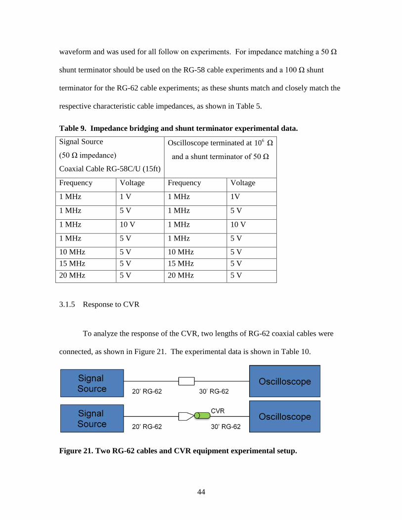
To analyze the response of the CVR, two lengths of RG-62 coaxial cables were
connected, as shown in Figure 21. The experimental data is shown in Table 10.
Figure 21. Two RG-62 cables and CVR equipment experimental setup.
45
Table 10. Two RG-62 cables and CVR experimental data. Signal Source
(50 Ω impedance)
Oscilloscope
(Terminated at 50 Ω) with two RG-62
(93 Ω) cables of 50ft combined
length
Oscilloscope
(Terminated at 50 Ω) with the two
RG-62 (93 Ω) cables and the CVR
placed in the middle
Frequency Voltage Frequency Voltage Frequency Current
1 MHz 1 V 1 MHz 0.96 V 0.93 MHz 0.05 A
1 MHz 5 V 1 MHz 4.76V 1.00 MHz 0.18 A
10 MHz 5 V 10 MHz 4.36 V 9.26 MHz 0.08 A
15 MHz 5 V 15 MHz 4.37 V 13.51 MHz 0.09 A
20 MHz 5 V 20 MHz 4.84 V 19.30 MHz 0.10 A
With a combined length of 50′ for the two RG-62 cables the expected voltage
drop, due to the characteristic impedance of the two cables, was measured on the
oscilloscope. These cables have a characteristic impedance of 93 Ω, and would not be
impedance matched with either the signal source or the signal load of 50 Ω. This
produced destructive interference, reducing VL. At high frequencies, the total reactance
and the skin effect increase. Both of these effects cause a decrease in VL. With the CVR
in place, a resonant frequency (ω0) of approximately 1 MHz was found, as a maximum
current of 0.18 (A) was measured for the 1 MHz, 5 V source. This current was calculated
using the 0.02651 Ω CVR. Resonance was approached at frequencies above 10 MHz as
current began to increase again. When the CVR is placed in the system the measured
current frequency deceases. This is likely do to circuit impedance differences between
the coaxial cable and the CVR which resulted in reduced energy transfer and lower
voltage.

46
3.1.6 Response to CVR Location The purpose of these experiments was to find the best cable and connector
attachment that would maximize the power throughput. In other words to find the best
impedance matched circuit. The CVR was placed in numerous locations along the VDG
and the power measured on the oscilloscope for a variety of sinusoidal waveforms. The
two best matches where found when the CVR was placed in position A and position B, as
shown in Figure 22. Position A was measured 12″ from the base plate along the support
cable. Position B was measured 63″ from the base plate along the support cable, and
Position C was measured 6″ from the intersection of the support cable and the strike plate
pole. These three CVR positions (position A, B and C) will be used to describe CVR
location throughout this thesis. The response to the CVR in position A and position B
will be described in this section.
Figure 22. Position A, B and C for CVR locations.

47
These experiments were conducted with a constant frequency of 1 MHz, with
peak voltages varying from 1-10 volts. This was then repeated, but this time the voltage
was kept constant at 5 volts while varying the frequency from 1-20 MHz. The VDG
circuit was set up by connecting the voltage source to the front of the strike plate using
alligator clips and copper foil tape, as shown in Figure 23. The experiments were
conducted with and without the CVR to determine CVR response. The data for the CVR
placed on the back of the strike plate is found in Appendix B. The data for CVR in
position B is shown in Table 11 and was compared to the data measured from position A
shown in Table 12.
Figure 23. Experimental setup with CVR at position B.
48
Table 11. Experimental data with CVR placed at position B.
Signal Source
(50 Ω impedance)
Without CVR
(The oscilloscope was
terminated at 50 Ω, RG-62
cables were used)
With CVR
(The oscilloscope was
terminated at 50 Ω, RG-62
cables were used)
Frequency Voltage Frequency Voltage Frequency Current
1 MHz 1 V 1 MHz 0.87 V 0.89 MHz 0.04 A
1 MHz 5 V 1 MHz 4.36 V 1 MHz 0.14 A
1 MHz 10 V 1 MHz 9.08 V 1 MHz 0.33 A
1 MHz 5 V 1 MHz 4.44 V 1 MHz 0.16 A
10 MHz 5 V 10 MHz 2.94 V 10 MHz 0.13 A
15 MHz 5 V 15 MHz 2.70 V 15 MHz 0.22 A
20 MHz 5 V 20 MHz 2.62 V 19.80 MHz 0.10 A
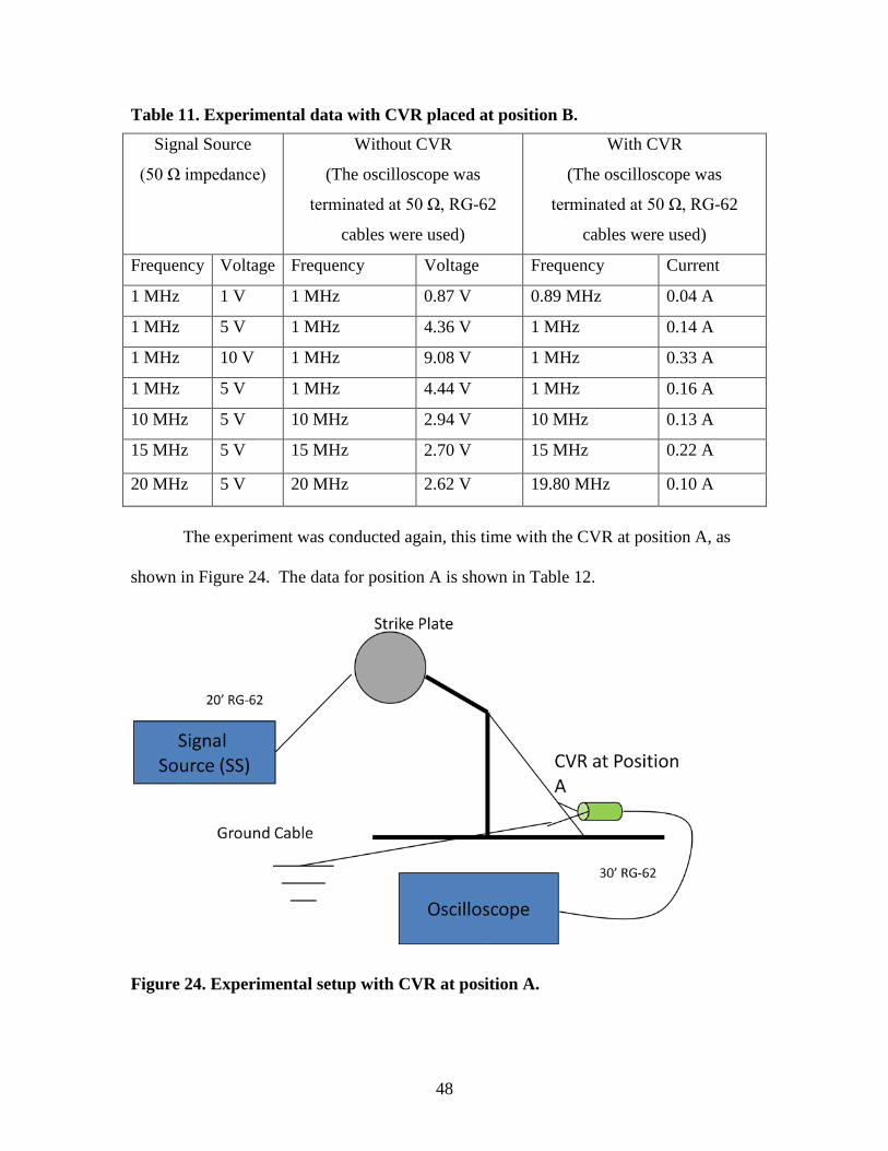
The experiment was conducted again, this time with the CVR at position A, as
shown in Figure 24. The data for position A is shown in Table 12.
Figure 24. Experimental setup with CVR at position A.

49
The experiment was conducted to investigate the effect of the additional length of the
support cable on the circuit response. Comparing Table 12 to Table 11, without the
CVR, all but the 10 MHz frequency had a greater voltage drop than at position B. This
was likely due to impedance mismatching, and added resistance from the extra support
cable length. The increase of VL found at 10 MHz for position A is likely due to the
oscilloscope responding to a resonance frequency within the circuit.
When the CVR was placed at position A, the measured current was higher than
when attached at position B for all frequencies except the 20 MHz range. This showed
that there was a closer impedance match with the CVR at position A. This was also true
for all other measured locations.
Table 12. Experimental data with CVR at position A. This is the best impedance match found.
Signal Source
(50 Ω impedance)
Without CVR (Oscilloscope terminated at 50 Ω)
With CVR (Oscilloscope terminated at 50 Ω)
With CVR (Oscilloscope terminated at
610 Ω & 100Ω shunt terminator)
Frequency Voltage Frequency Voltage Frequency Current Frequency Voltage
1 MHz 1 V 1 MHz 0.86 V 1 MHz 0.05 A 0.99 MHz 0.12 A
1 MHz 5 V 1 MHz 4.34 V 0.97 MHz 0.17 A 1 MHz 0.24 A 1 MHz 10 V 1 MHz 8.84 V 1 MHz 0.33 A 1 MHz 0.41 A 1 MHz 5 V 1 MHz 4.36 V 1 MHz 0.17 A 1 MHz 0.26 A 10 MHz 5 V 10 MHz 3.24 V 10 MHz 0.26 A 10 MHz 0.64 A 15 MHz 5 V 15 MHz 1.28 V 15 MHz 0.53 A 15 MHz 0.75 A 20 MHz 5 V 20 MHz 1.05 V 18.9 MHz 0.08 A 18.2 MHz 0.16 A

50
Because of the higher VL measurements with the CVR placed at position A versus
any other location, an additional experiment was conducted, but this time the oscilloscope
was terminated at 610 Ω, and a shunt terminator of 100 Ω was added in parallel, as shown
in Table 12 as the last column. This significantly increased the measured current (greater
than any other setup or CVR location). This experiment showed that positioning the
CVR at position A and terminating the oscilloscope at 610 Ω, as well as adding a shunt
termination of 100 Ω in parallel, resulted in the best impedance match found, and was
used for all follow on experiments.
3.1.7 Summary of Equipment Confidence Experiments
When the CVR was placed into the experiments, it was shown that the signal
source had to be greater than 1 volt with a frequency greater than 100 kHz. If not, the
oscilloscope was dominated by background noise. As the strikes from the VDG were in
the thousands of volts and had frequency components in the MHz range, this was not a
problem during the VDG pulse experiments. The signal source generator had a
maximum output of 20 MHz and 10 volts; therefore, no equipment confidence
experiments were conducted above these limits.
As described in the preceding sections, the characteristic impedance of the
equipment and cables, as well as the resonant frequency, skin effect, reflections, and
bridging/terminators, all affected the data. The use of the RG-62 shielded coaxial cables
terminated into the oscilloscope at 106 Ω, and shunt terminator of 100 Ω, transferred the
greatest power to the oscilloscope with the least interference, as shown in Table 12, and
was used throughout all of the remaining experiments. It was also determined that when

51
the CVR is placed at position A, as shown in Figure 22 there is a resonant frequency of
15 MHz, as shown in Appendix B, as the maximum power (e.g. voltage) was measured.
3.2 Response to VDG Equipment Setup
A schematic of the major equipment components and general VDG experiment is
shown in Figure 25. The VDG was moved 1 to 18″ away from the strike plate to find the
results of spark gap distance. The oscilloscope was kept on a 3′ high table placed 4′
outside the VDG room to minimize EMI. The control station for the belt roller motor
was placed inside the VDG room, and the 20kV high voltage source was supported off
the ground with a wooden stool 3′ away from the VDG. The 30′ aluminum taped RG-62
coaxial cable was supported off the ground by two plastic columns, so as to minimize
EMI and ground current coupling.
Figure 25. The Van de Graaff experimental setup used for all VDG experiments. A 20 kV high voltage source was used to speed up the charging of the VDG
capacitance, as described in Section 2.1. It was determined by experiment that the

52
current pulse amplitude and major frequency components of the wave were unaffected by
the magnitude of the high voltage input. It did, however, increase the frequency of strike
discharges between the VDG and strike plate. It was also found that the discharge would
impact the strike plate, causing the strike plate to move in between strikes, which
momentarily changed the spark gap distance. Through trial and error experiments, a
minimum of 6 (s) was needed between strikes for the strike plate to fully return to its
original location and stabilize the spark gap. Therefore, the high voltage source was kept
as low as possible, so as to produce strikes between 7 and 8 (s).
It was also determined that the speed of the motor that turns the VDG belt did not
affect the waveform. However, it also impacted the frequency of the discharges. To
reduce the number of variables, the motor was kept at 30 RPM for all experiments and
the high voltage was manipulated to control the time interval to a minimum of 7 (s)
between strikes.
If the spark gap was too great a strike would not occur. The maximum spark gap
was found to be between 9 and 18″, depending upon environmental conditions (e.g.
humidity, temperature and wind). It was also found that spark gaps greater than 9″ gave
very erratic current pulses (i.e. large amplitude, and variable frequency of oscillation)
making the VDG unpredictable. It is likely (and was qualitatively observed) that for
larger spark gaps, the current path and strike point would substantially change for a set of
strikes. Wind travelling through the room (via poorly sealed windows or an open door)
also reduced the frequency of strikes and the maximum spark gap. This is likely due to
the wind removing ionized atoms, such as ozone, that would assist in initiating the strike.
On days when the wind was not blowing the current pulses would stabilize after 20

53
strikes. Therefore, for each experiment, a set of conditioning strikes were measured until
the current pulses were consistent. Then data would be collected.
With numerous trial and error experiments it was found that the connection of the
CVR was critical for reliable and repeatable current pulses. It was found that a poor
CVR connection could give momentary good results but then the current pulse would
change. It was observed, at times, that a small spark gap resulted from poor CVR
connections to the cable. Therefore, copper mesh clamps were used to better connect
the CVR to the support cable, as shown in Figure 26. This resulted in a noticeable
difference in the current pulse, in which fewer frequency components were observed, and
measured by FFT. The primary difference was that the first oscillation became the
maximum peak of the current pulse, after which the signal was fully damped.
Figure 26. Copper mesh clamps were used to connect the CVR to the support cable and additional resistors. It was also found by trial and error experiments that to have repeatable current
pulses all equipment had to be isolated, as much as possible, from the concrete floor, as

54
shown in Figure 27. The next critical setup procedure was placement of the RG-62
shielded coaxial cable. The cable was positioned on support material and configured as
shown in Figure 28. Once the VDG equipment was isolated from the concrete floor, the
CVR had a solid connection, and the RG-62 cable was positioned so as to produce a
maximum peak current in the first oscillation, reliable and repeatable current pulses were
obtained. For the repeatable experiments, once a current pulse was measured in which
the first oscillation was statistically (frequency and amplitude measured) stable, the RG-
62 shielded cable was not moved for the rest of the experiments, as shown in Figure 28.
Figure 27. All VDG system equipment was isolated from the concrete floor.
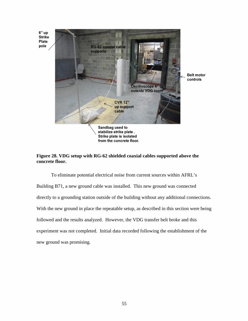
55
Figure 28. VDG setup with RG-62 shielded coaxial cables supported above the concrete floor. To eliminate potential electrical noise from current sources within AFRL’s
Building B71, a new ground cable was installed. This new ground was connected
directly to a grounding station outside of the building without any additional connections.
With the new ground in place the repeatable setup, as described in this section were being
followed and the results analyzed. However, the VDG transfer belt broke and this
experiment was not completed. Initial data recorded following the establishment of the
new ground was promising.
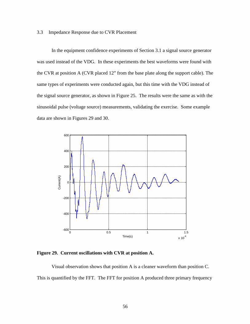
56
3.3 Impedance Response due to CVR Placement
In the equipment confidence experiments of Section 3.1 a signal source generator
was used instead of the VDG. In these experiments the best waveforms were found with
the CVR at position A (CVR placed 12″ from the base plate along the support cable). The
same types of experiments were conducted again, but this time with the VDG instead of
the signal source generator, as shown in Figure 25. The results were the same as with the
sinusoidal pulse (voltage source) measurements, validating the exercise. Some example
data are shown in Figures 29 and 30.
Figure 29. Current oscillations with CVR at position A. Visual observation shows that position A is a cleaner waveform than position C.
This is quantified by the FFT. The FFT for position A produced three primary frequency
0 0.5 1 1.5
x 10-6
-600
-400
-200
0
200
400
600
Time(s)
Cur
rent
(A)

57
components, while position C gave four primary frequency components. “Primary”, in
this case, was defined as having at least a Fourier magnitude of 103 10× , as shown in
Figure 31.
Figure 30. Current oscillations with CVR at position C.
Figure 31. Plot of FFTs of full current pulses measured with the CVR at position A (blue) and position C (red).
0 0.2 0.4 0.6 0.8 1 1.2 1.4 1.6 1.8 2
x 10-6
-600
-400
-200
0
200
400
600
Time (s)
Cur
rent
(A)
0 0.5 1 1.5 2 2.5 3 3.5 4 4.5 5
x 107
0
1
2
3
4
5
6
7
8x 10
11
Frequency (Hz)
Four
ier T
rans
form
(Arb
. Uni
ts)
CVR at Position ACVR at Position C

58
Charlesworth and Staniforth’s results confirm the data that was found in this
thesis. They state a dominant frequency was excited in large [12] and small [5] VDGs
(10 MV and 5 MV respectively) due to “…the inductance of the VDG resonating with
the spark channel inductance. In some cases, a higher frequency, which is an
electromagnetic mode supported by the whole machine, is also excited” [12]. The
dominant frequency was spark gap and maximum potential dependent. A lower
frequency of 31 ± 3.5 MHz and a higher frequency of 186 ± 17 MHz was found for the
small 1.5 MV VDG [5]. An additional lower frequency of 10 to 13 MHz, and a higher
frequency of 110 ± 20 MHz was measured for the shorter spark gaps and 230 ± 25 MHz
for large spark gaps for the 10 MV VDG [12]. Both studies state “these higher end
frequencies are probably associated with the high frequency electromagnetic modes
which can be supported by the whole machine” [12] [5]. The VDGs used in these
studies were enclosed and pressurized [5][12], but it was assumed that these methods are
applicable for the present study.
The AFRL VDG was found to have three primary frequencies within the current
pulse, compared to the two found for the Charlesworth and Staniforth studies. The same
raw data that was used for the impedance matching and CVR location experiments,
shown in Figure 29 and Figure 30 were used to analyze the frequency components via
FFT. The FFT data, plotted in Figure 31 for both the CVR at position A and position C
have a primary FFT of 8 MHz ± 1 MHz. They also both share a secondary dominant
frequency of 2 MHz, but the tertiary dominant frequency components vary from 15 MHz
for position A to 29 and 34 MHz for position C. The FFT algorithm confirms what the

59
raw data showed, which is, that attaching the CVR at position A results in a cleaner
(fewer interference oscillations, likely due to better impedance matching), current pulse.
As another example, the FFT analysis was also applied to the current pulses
measured with the CVR placed at position B. These results are shown in Figure 40. It is
clear from this data that the primary frequency of 8 MHz is not as clearly defined as
when the CVR was placed at position A or B.
Using both raw data and FFT analysis, it was proven that the cleanest signal (e.g.
one with the fewest dominant frequency components) resulted with the CVR attached at
position A. Positions A, B and C were the cleanest current pulses over all other
locations. Therefore, position A was chosen for all follow on experiments.
Figure 32. FFT of the current pulse measured with CVR at position B.
0 1 2 3 4 5 6 7 8 9 10 11 x 10 7
0
5
10
15 x 10 7
Frequency Hz
Four
ier T
rans
form
(Arb
. Uni
ts)

60
3.4 Response due to Spark Gap
Once the CVR location of position A was determined to produce the cleanest
current pulse; which allowed repeatable strikes to take place, the effort was oriented on
finding the least noisy measurement based upon the spark gap distance. The same
method as in Section 3.3 was used. This method was to qualitatively assess the raw data
waveform, followed by a FFT to determine the measurement with the least number of
major oscillation frequencies. The time dependent current for the 3″ spark gap, as shown
in Figure 33, had fewer reflections and frequencies (on top of the primary current) than
did the 7″ spark gap, also shown in Figure 33. From all raw data qualitatively observed
and recorded, the 3″ spark gap produced the best impedance match over any other spark
gap distance.
Figure 33. Current pulse for the 3″ and 7″ spark gaps.
0 0.2 0.4 0.6 0.8 1 1.2 1.4
x 10-6
-600
-400
-200
0
200
400
600
Time (s)
Cur
rent
(A)
3" Spark Gap7" Spark Gap

61
Observation of the raw data showed that the 3″ spark gap produced the cleanest
current pulse, as shown in Figure 33. However, the FFT for the spark gaps ranging from
1 to 8″ were all within ± 0.3 MHz for all three major frequencies. The primary
frequency was measured at 7.5 MHz while the secondary frequency was measured at 2
MHz, and finally the tertiary frequency was found to be 14 MHz. These measurements
were conducted with alligator clips for the CVR connection verses the copper mesh
clamps. These results are ± 1.5 MHz different from those measured with mesh clamps,
as shown in Tables 14-17. Nevertheless, the FFT results lead to the conclusion that the
spark gaps of 3, 6, 7 and 8″ should be used for the repeatable experiments.
3.5 Reliable and Repeatable Current Strikes
3.5.1 Environmental Set up It was found that to achieve four days of repeatable current pulses the set up of the
VDG system was critical and that Section 3.2 (VDG Equipment Set up) needs to be
followed. Power projections through the measurement circuit were critical to the
placement of the 30′ RG-62 shielded coaxial cable. Previous experiments showed that
placement of the cable could change the current amplitude by up to 117 (A). Positioning
the cable, on the concrete floor, lead to the greatest decrease in the measured current. It
was found that the RG-62 shielded coaxial cable must be supported off the ground, as
ground current coupling takes place. It was also found that positioning the cable changed
the amplitude and frequencies of the current pulses. Therefore, the cable was positioned
to create an environment where the first current oscillation had the maximum current

62
amplitude. Once a suitable cable position was found it was kept in that position, as
shown in Figure 28. The only time it was moved was when spark gap distance was
changed.
3.5.2 Measurements with Repeatable First Oscillations The four days of experiments had only slightly different humidity and
temperature environments for the VDG room. These conditions are shown in Table 13.
All experiments had the CVR placed at position A. Comparing current pulses for the 3″
spark gap for experiment 1 to experiment 2 showed that the first oscillations of both data
sets share the same measured frequency of 8.56 MHz ± 0.4 MHz and approximate
maximum current amplitudes of 200 (A); however, the amplitudes of the 2nd through 8th
oscillations are distinctly different, as shown in Figure 34.
Table 13. Humidity and temperature environments for the repeatable experiments.
Experiment Humidity Temperature (Fahrenheit)
1 21% 68
2 16-21% 68
3 20% 63
4 41% 72

63
Figure 34. Raw data (current as a function of time) for 3″ spark gap. The data obtained for all repeatable experiments did not represent a damped sine
wave. Nevertheless, the first oscillation rise and fall times, and maximum amplitude
were repeatable. It was assumed that only the first oscillation is repeatable because the
rise time of the first oscillation is completed before the transmission of the reflections
have time to travel through the 30′ coaxial cable.
The signal propagation through the RG-62 cable is 0.840c, with c being the speed
of light measured at 83 10× m/s [17]. Therefore, the transmission time of a reflection
through a 30′ coaxial cable is 83.63 10 ( ).s−× The rise time of the average first oscillation
for the spark gap of 3″ is 8 81.5 10 0.3 10 ( ).s− −× ± × This was the shortest rise time, while
the 7″ spark gap had the longest rise time of 8 81.0 10 0.3 10 ( ).s− −× ± × Therefore, it is
assumed that the first oscillation is repeatable because reflected waves from the pulse
cannot traverse the cable in time to interfere.
0 0.2 0.4 0.6 0.8 1 1.2
x 10-6
-300
-200
-100
0
100
200
300
Time (s)
Cur
rent
(A)
Experiment 1Experiment 2
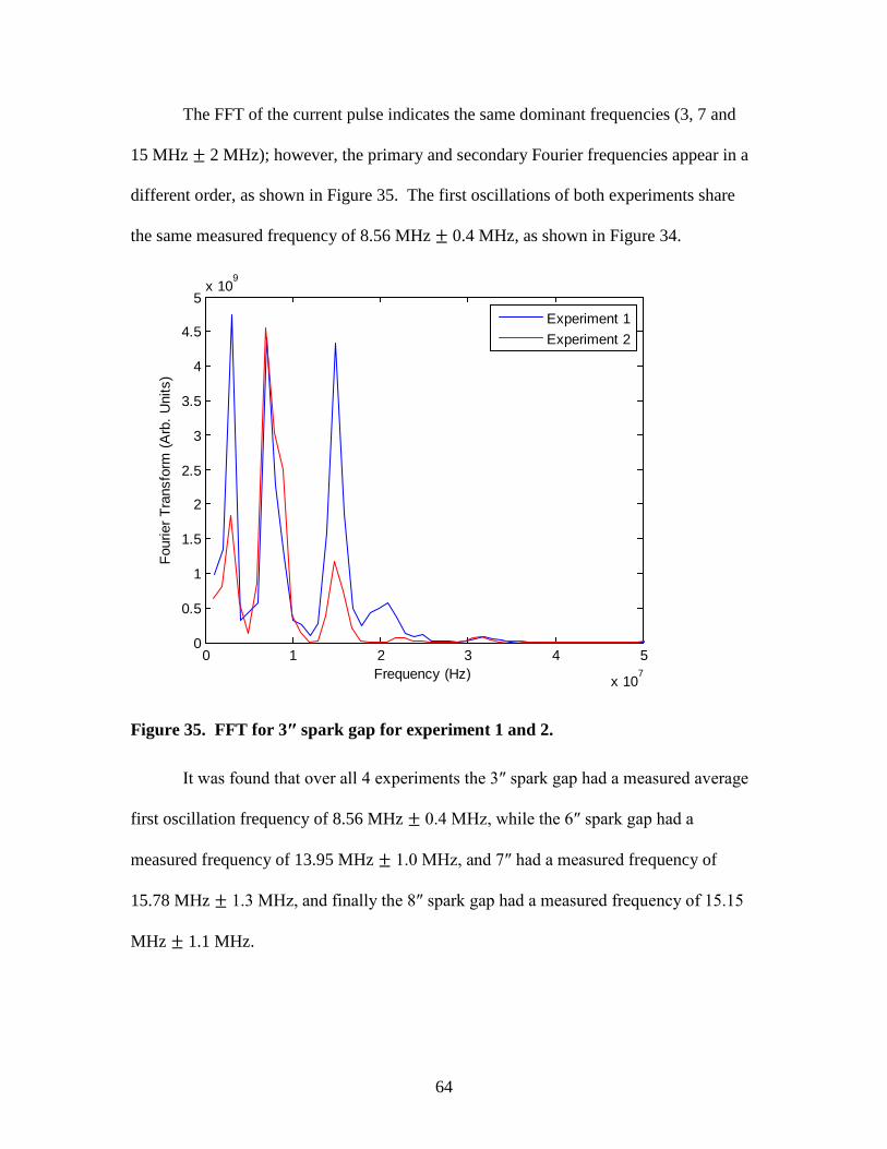
64
The FFT of the current pulse indicates the same dominant frequencies (3, 7 and
15 MHz ± 2 MHz); however, the primary and secondary Fourier frequencies appear in a
different order, as shown in Figure 35. The first oscillations of both experiments share
the same measured frequency of 8.56 MHz ± 0.4 MHz, as shown in Figure 34.
Figure 35. FFT for 3″ spark gap for experiment 1 and 2. It was found that over all 4 experiments the 3″ spark gap had a measured average
first oscillation frequency of 8.56 MHz ± 0.4 MHz, while the 6″ spark gap had a
measured frequency of 13.95 MHz ± 1.0 MHz, and 7″ had a measured frequency of
15.78 MHz ± 1.3 MHz, and finally the 8″ spark gap had a measured frequency of 15.15
MHz ± 1.1 MHz.
0 1 2 3 4 5
x 107
0
0.5
1
1.5
2
2.5
3
3.5
4
4.5
5x 10
9
Frequency (Hz)
Four
ier T
rans
form
(Arb
. Uni
ts)
Experiment 1Experiment 2
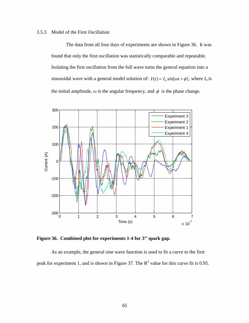
65
3.5.3 Model of the First Oscillation
The data from all four days of experiments are shown in Figure 36. It was
found that only the first oscillation was statistically comparable and repeatable.
Isolating the first oscillation from the full wave turns the general equation into a
sinusoidal wave with a general model solution of: 0( ) sin[ ]I t I tω φ= + , where Io is
the initial amplitude, ω is the angular frequency, and φ is the phase change.
Figure 36. Combined plot for experiments 1-4 for 3″ spark gap. As an example, the general sine wave function is used to fit a curve to the first
peak for experiment 1, and is shown in Figure 37. The R2 value for this curve fit is 0.95.
0 1 2 3 4 5 6 7
x 10-7
-300
-200
-100
0
100
200
300
Time (s)
Cur
rent
(A)
Experiment 3Experiment 2Experiment 1Experiment 4

66
Figure 37. Curve fitted plot for the first oscillation for the data of experiment 1. The spark gap is 3″.
3.5.4 Measurement of Current Amplitudes and Frequencies
The data measured with spark gaps of 3, 6, 7 and 8″ were chosen to analyze the
consistency of the spark system. The current amplitude of each first oscillation was
analyzed using a sine function fit, and FFT was used to analyze the full current pulse for
the dominate frequencies. The results are shown in Tables 14 through 17 with a
summary in Tables 26.
0 1 2 3 4 5 6 7
x 10-8
0
50
100
150
200
250
Time (s)
Cur
rent
(A)
Experiment 1fitted curve
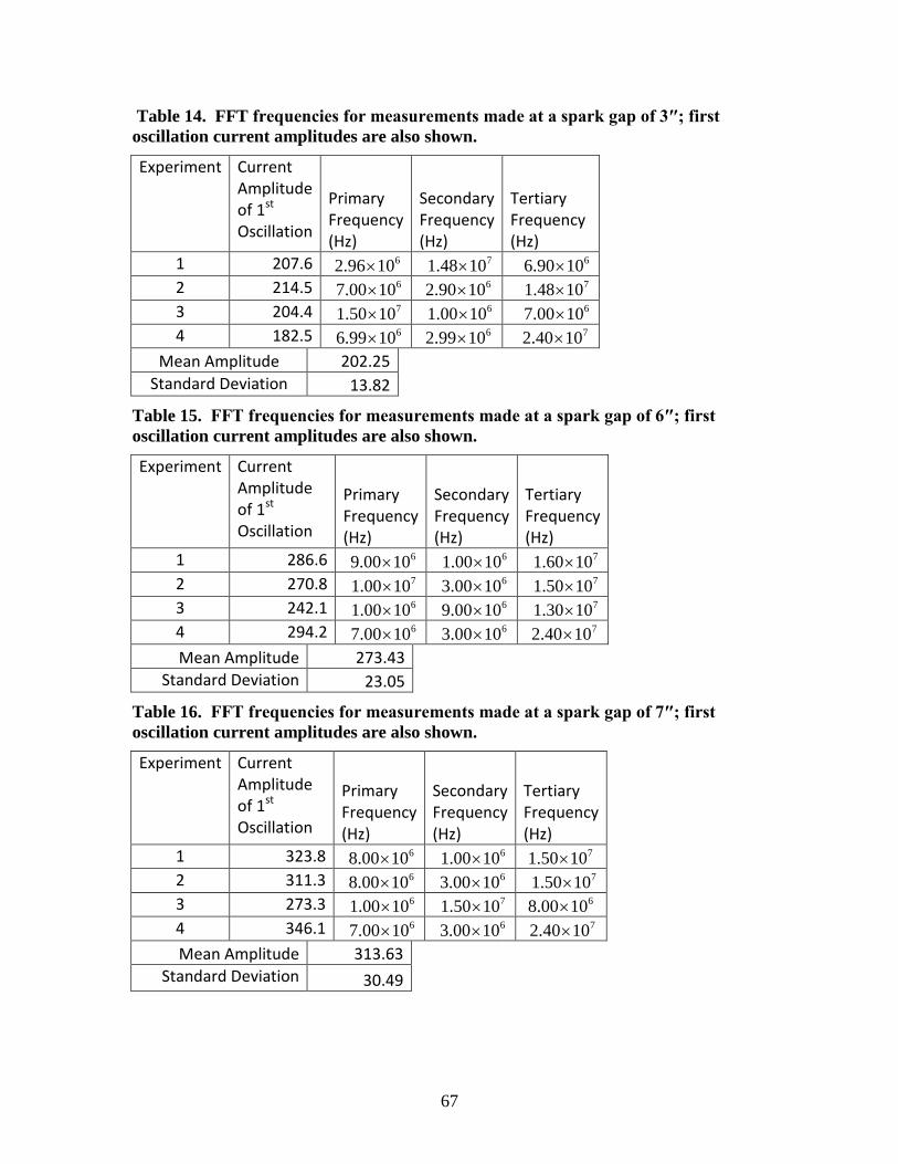
67
Table 14. FFT frequencies for measurements made at a spark gap of 3″; first oscillation current amplitudes are also shown.
Experiment Current Amplitude of 1st Oscillation
Primary Frequency (Hz)
Secondary Frequency (Hz)
Tertiary Frequency (Hz)
1 207.6 62.96 10× 71.48 10× 66.90 10× 2 214.5 67.00 10× 62.90 10× 71.48 10× 3 204.4 71.50 10× 61.00 10× 67.00 10× 4 182.5 66.99 10× 62.99 10× 72.40 10×
Mean Amplitude 202.25 Standard Deviation 13.82 Table 15. FFT frequencies for measurements made at a spark gap of 6″; first
oscillation current amplitudes are also shown.
Experiment Current Amplitude of 1st Oscillation
Primary Frequency (Hz)
Secondary Frequency (Hz)
Tertiary Frequency (Hz)
1 286.6 69.00 10× 61.00 10× 71.60 10× 2 270.8 71.00 10× 63.00 10× 71.50 10× 3 242.1 61.00 10× 69.00 10× 71.30 10× 4 294.2 67.00 10× 63.00 10× 72.40 10× Mean Amplitude 273.43
Standard Deviation 23.05 Table 16. FFT frequencies for measurements made at a spark gap of 7″; first
oscillation current amplitudes are also shown.
Experiment Current Amplitude of 1st Oscillation
Primary Frequency (Hz)
Secondary Frequency (Hz)
Tertiary Frequency (Hz)
1 323.8 68.00 10× 61.00 10× 71.50 10× 2 311.3 68.00 10× 63.00 10× 71.50 10× 3 273.3 61.00 10× 71.50 10× 68.00 10× 4 346.1 67.00 10× 63.00 10× 72.40 10× Mean Amplitude 313.63
Standard Deviation 30.49

68
Table 17. FFT frequencies for measurements made at a spark gap of 8″; first oscillation current amplitudes are also shown.
Experiment Current Amplitude of 1st Oscillation
Primary Frequency (Hz)
Secondary Frequency (Hz)
Tertiary Frequency (Hz)
1 350.8 61.00 10× 68.00 10× 71.50 10× 2 369.4 67.00 10× 63.00 10× 71.40 10× 3 324.4 61.00 10× 71.50 10× 67.00 10× 4 372.5 67.00 10× 63.00 10× 72.40 10× Mean Amplitude 354.23
Standard Deviation 22.10
Figure 38 shows that the first oscillation has the mean maximum current, as well
as the mean frequency, rise as a function of spark gap distance. The rise is because
current is a function of voltage and power. It takes more power to strike across longer
distances; therefore current, voltage and frequency rise as spark gap distance is increased.
The 3″ spark gap data resulted in the smallest standard deviation for current
amplitude compared to 6, 7, and 8″. The 3″ spark gap resulted in currents with a mean
value of 202.25 ± 13.82 (A) and rise to the 8″ spark gap of 354.23±22.10 (A). As shown
in Tables 14-17. For the first three experiments the FFT data for the full current pulses
produced three dominant frequency components of 3, 7 and 15 MHz ± 2 MHz. The
position of the primary to tertiary dominant frequencies changed, but all three days
shared the same frequencies for the full wave. The FFT data for experiment 4 shared the
3 and 7 MHz ± 2 MHz for all spark gaps, but its tertiary frequency was 24 MHz
compared to the 15 MHz ± 1.5 MHz, found on the three previous experiments.
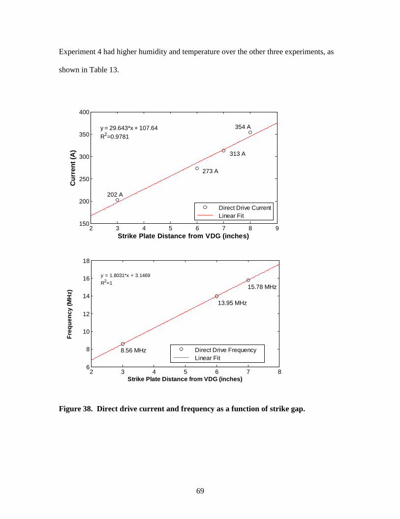
69
Experiment 4 had higher humidity and temperature over the other three experiments, as
shown in Table 13.
Figure 38. Direct drive current and frequency as a function of strike gap.
2 3 4 5 6 7 8 9150
200
250
300
350
400
Strike Plate Distance from VDG (inches)
Cur
rent
(A)
y = 29.643*x + 107.64R2=0.9781
Direct Drive Current Linear Fit
354 A
313 A
273 A
202 A
2 3 4 5 6 7 86
8
10
12
14
16
18
Strike Plate Distance from VDG (inches)
Freq
uenc
y (M
Hz)
y = 1.8031*x + 3.1469R2=1
Direct Drive Frequency Linear Fit
15.78 MHz
8.56 MHz
13.95 MHz

70
3.5.5 Curve Fitting of the First Oscillation
Curve fitting the data to the sine wave function of 0( ) sin[ ]I t I tω φ= + is achieved
by isolating the first oscillation from the rest of the data. The general models for the 3, 6,
7 and 8″ spark gap distances, as well as the goodness of fit data for each distance, are
shown in Tables 18-25 with a summary in Table 27. The curve fit for experiment 3, for a
spark gap of 3″, gave the best curve fit out of all of the spark gaps investigated, yielding
an R2 value 0.983, this is illustrated in Figure 39.
Table 18. Curve fit parameters for the first oscillations of current pulses measured with a spark gap distance of 3″, for the general model of 0( ) sin[ ]I t I tω φ= + .
Experiment General Model Solution:
0( ) sin[ ]I t I tω φ= +
95% Confidence Bounds I0 low
I0 high
ω low
ω high
Φ low
Φ high
1 7196.4sin[5.04 10 0.263]x t − 186.6 206.1 74.9 10× 75.2 10× -0.34 -0.19
2 7209.4sin[5.51 10 0.104]x t − 206.6 212.1 75.5 10× 75.6 10×
-0.13 -0.08
3 7201.7sin[5.52 10 0.109]x t − 195.9 207.4 75.4 10× 75.6 10× -0.15 -0.07
4 7181.0sin[5.46 10 0.097]x t − 173.8 188.2 75.3 10× 75.7 10×
-0.16 0.04
Mean 7197.1sin[5.38 10 0.143]x t − 190.7 203.5 75.2 10× 75.5 10× -0.19 -0.08 Std Dev 0I =
12 ω =
2.3E6 φ =
0.08 13.93 10.49 62.7 10× 62.0 10×
0.10 0.09
Table 19. Goodness of fit statistics for the first oscillation of current pulses measured with a spark gap distance of 3″.
Experiment R2 SSE Adjusted R2 RMSE
1 0.950 9803 0.944 17.78
2 0.975 15760 0.974 10.69
3 0.983 2723 0.982 9.86
4 0.963 3761 0.961 12.03

71
Figure 39. The best curve fit data was for experiment 3, and is for the spark gap of 3″. This curve fit has an R2 value of 0.983. The 3″ spark gap resulted in the best R2 data over the 4 experiments. The average
solution for the 3″ spark gap over all four experiments is shown in Figure 40, along with
the low current amplitude data point given on experiment 4 and the high current
amplitude data point given on experiment 2. The averaged solution including the
standard deviation is shown in Figure 41.
0 1 2 3 4 5 6 7
x 10-8
0
50
100
150
200
250
Time (s)
Cur
rent
(A)
Experiment 3fitted curve
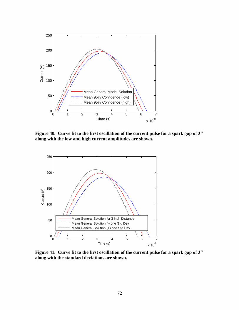
72
Figure 40. Curve fit to the first oscillation of the current pulse for a spark gap of 3″ along with the low and high current amplitudes are shown.
Figure 41. Curve fit to the first oscillation of the current pulse for a spark gap of 3″ along with the standard deviations are shown.
0 1 2 3 4 5 6 7
x 10-8
0
50
100
150
200
250
Time (s)
Cur
rent
(A)
Mean General Model SolutionMean 95% Confidence (low)Mean 95% Confidence (high)
0 1 2 3 4 5 6 7
x 10-8
0
50
100
150
200
250
Time (s)
Cur
rent
(A)
Mean General Solution for 3 inch DistanceMean General Solution (-) one Std DevMean General Solution (+) one Std Dev

73
Table 20. Curve fit parameters for the first oscillations with a spark gap of 6″ for the general model of 0( ) sin[ ]I t I tω φ= + .
Experiment General Model Solution:
0( ) sin[ ]I t I tω φ= +
95% Confidence Bounds I0 low
I0 high
ω low
ω high
Φ low Φ high
1 7272.9sin[9.24 10 0.052]x t − 252.9 292.8 78.7 10× 79.8 10× -0.06 0.17 2 7251.0sin[9.30 10 0.236]x t − 247.3 255 79.2 10× 79.4 10× -0.26 -0.21 3 7212.1sin[8.277 10 0.126]x t − 185.4 238.9 77.4 10× 79.1 10× -0.31 -0.06 4 7237.5sin[8.27 10 0.077]x t − 206.6 268.4 77.4 10× 79.1 10× -0.27 0.12
Mean 7243.45sin[8.77 10 0.123]x t − 223.1 263.8 78.2 10× 79.4 10× -0.23 0.02 Std Dev 0I =
25.4 ω =
65.8 10× φ =
0.08 32.49 22.8 68.9 10× 63.1 10× 0.11 0.17
Table 21. Goodness of fit statistics for the first oscillation with a spark gap of 6″.
Date R2 SSE Adjusted R2 RMSE
16/11/12 0.941 9471 0.941 25.13
17/11/12 0.937 1.80E5 0.937 23.14
29/11/12 0.871 2.21E4 0.855 36.04
4/12/12 0.856 2.94E4 0.856 41.56
Table 22. Curve fit parameters for the first oscillations with a spark gap of 7″ for the general model of 0( ) sin[ ]I t I tω φ= + .
Experiment General Model Solution:
0( ) sin[ ]I t I tω φ= +
95% Confidence Bounds I0 low
I0 high
ω low
ω high
Φ low
Φ high
1 7311sin[9.24 10 0.116]x t − 286.4 335.5 78.7 10× 79.8 10× -0.23 0.02 2 7301sin[10.28 10 0.059]x t − 298.3 303.4 81.0 10× 81.1 10× -0.07 0.05 3 7271sin[10.91 10 0.009]x t − 263.4 278.7 81.1 10× 81.1 10× -0.03 0.05 4 7295sin[9.24 10 0.082]x t − 262.7 327.1 78.5 10× 81.0 10× -0.24 0.08
Mean 7294.5sin[9.92 10 0.067]x t − 277.7 311.2 79.5 10× 81.1 10× -0.14 0.04 Std Dev 0I =
17 ω =
68.24 10× φ =
0.04 17.6 25.6 71.1 10× 66.2 10× 0.11 0.03

74
Table 23. Goodness of fit statistics for the first oscillation with a spark gap of 7″.
Experiment R2 SSE Adjusted R2 RMSE
1 0.943 1.44E4 0.935 31.02
2 0.980 7.39E4 0.980 15.01
3 0.992 893.5 0.991 8.63
4 0.894 2.48E4 0.879 40.63
Table 24. Curve fit parameters for the first oscillations with a spark gap of 8″ for the general model of 0( ) sin[ ]I t I tω φ= + .
Experiment General Model Solution:
0( ) sin[ ]I t I tω φ= +
95% Confidence Bounds I0 low
I0 high
ω low
ω high
Φ low
Φ high
1 7326.5sin[8.73 10 0.057]x t − 298.0 354.7 78.1 10× 79.3 10× -0.19 0.07 2 7350.9sin[10.3 10 0.076]x t − 348.0 353.7 81.0 10× 81.0 10× -0.09 -0.06 3 7315.1sin[9.82 10 0.098]x t − 298.0 332.0 79.4 10× 81.0 10× -0.18 -0.02 4 7321.5sin[9.24 10 0.089]x t − 288.2 354.8 78.5 10× 81.0 10× -0.24 0.06
Mean 7328.5sin[9.52 10 0.080]x t − 308.1 348.8 79.1 10× 81.0 10× -0.17 0.01 Std Dev 0I =
15.6 ω =
66.8 10× φ = .02
27.0 11.21 69.5 10× 64.7 10× 0.06 0.07
Table 25. Goodness of fit statistics for the first oscillation with a spark gap of 8″.
Experiment R2 SSE Adjusted R2 RMSE
1 0.930 2.17E4 0.921 36.8
2 0.981 8.63E4 0.981 16.47
3 0.972 6190 0.968 21.03
4 0.903 2.66E4 0.890 42.08

75
Table 26. Summary of the maximum current of the first pulse as a function of spark gap.
Spark Gap(inches) Max Current Mean/Average
(amps)
Standard Deviation (amps)
3 202.25 13.82
6 273.43 23.05
7 313.63 30.49
8 354.23 22.10
Table 27. Summary of the average parameters for the first current oscillations as a function of spark gap distance.
Spark
Gap(inches)
General Model Mean/Average Solution:
0( ) sin[ ]I t I tω φ= +
Standard Deviation
I0 ω Φ
3 7197.1sin[5.38 10 0.143]x t − 0I =12 ω = 62.3 10× φ =0.08
6 7243.45sin[8.77 10 0.123]x t − 0I =25.4 ω = 65.8 10× φ =0.08
7 7294.5sin[9.92 10 0.067]x t − 0I =17 ω = 68.2 10× φ =0.04
8 7328.5sin[9.52 10 0.080]x t − 0I =15.6 ω = 66.8 10× φ =0.02
3.6 Results of Added Circuit Resistance As shown in Section 2.4, the overdamped or critically damped RLC circuit
current waveform best fits the free-field MIL-STD 464 standard test pulse. The critical
resistance in damping the VDG system is the spark gap resistance Rs(t), as shown in
Equation (15). This controlling resistance has three independent variables. They are the
air density (before air breakdown), length of the spark gap, and the time-dependent

76
current of the spark gap. It is this time dependent current that causes Rs(t) to decrease
with time.
The current in the spark gap cannot be measured directly, and the air density in
the VDG room cannot be easily modified, such as was done with gas pressure in [5].
Thus, the best variable for achieving an overdamped RLC circuit in this research was to
increase the spark gap resistance Rs(t), via the spark gap or increasing the circuit
resistance.
The data in Section 3.5.4 showed that the mean current increased as a function of
spark gap distance from 202 to 354 (A) as the spark gap length increased from 3 to 8″, as
shown in Figure 38. However, in all experiments the increased spark gap did not
increase Rs(t) to the point of taking the VDG from the underdamped RLC circuit to
overdamped.
A repeatable current was not obtained past 8″. Larger spark gaps lead to erratic
behavior owing to different spark paths/lengths, and eventually no strikes will occur. It
was found that to have a repeatable current waveform, the spark gap was limited to 8″.
Strikes were measured up to 18″; however, those strikes only occurred once or twice
before the strikes ceased altogether. To bring the strikes back, a much smaller spark gap
was needed. The strikes past 9″ were never repeatable; therefore, the distances of 3, 6, 7
and 8″ were used to characterize the direct current from the VDG. At these distances, the
VDG produced an underdamped waveform to the RLC circuit.
In an attempt to overdamp the VDG RLC circuit, ceramic resistors were added in
series with the CVR, as shown in Figure 34. The method was predicated upon the
theoretical analysis of Section 2.4. This section describes that in order to determine the
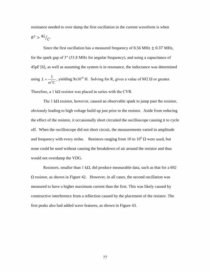
77
resistance needed to over damp the first oscillation in the current waveform is when
𝑅2 > 4𝐿𝐶� .
Since the first oscillation has a measured frequency of 8.56 MHz ± 0.37 MHz,
for the spark gap of 3″ (53.8 MHz for angular frequency), and using a capacitance of
45pF [6], as well as assuming the system is in resonance, the inductance was determined
using 2
1LCω
= , yielding 9x10⁻⁶ H. Solving for R, gives a value of 882 Ω or greater.
Therefore, a 1 kΩ resistor was placed in series with the CVR.
The 1 kΩ resistor, however, caused an observable spark to jump past the resistor,
obviously leading to high voltage build up just prior to the resistor. Aside from reducing
the effect of the resistor, it occasionally short circuited the oscilloscope causing it to cycle
off. When the oscilloscope did not short circuit, the measurements varied in amplitude
and frequency with every strike. Resistors ranging from 10 to 106 Ω were used, but
none could be used without causing the breakdown of air around the resistor and thus
would not overdamp the VDG.
Resistors, smaller than 1 kΩ, did produce measurable data, such as that for a 692
Ω resistor, as shown in Figure 42. However, in all cases, the second oscillation was
measured to have a higher maximum current than the first. This was likely caused by
constructive interference from a reflection caused by the placement of the resistor. The
first peaks also had added wave features, as shown in Figure 43.
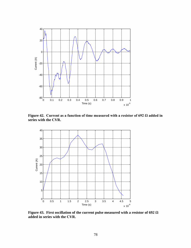
78
Figure 42. Current as a function of time measured with a resistor of 692 Ω added in series with the CVR.
Figure 43. First oscillation of the current pulse measured with a resistor of 692 Ω added in series with the CVR.
0 0.1 0.2 0.3 0.4 0.5 0.6 0.7 0.8 0.9 1
x 10-6
-80
-60
-40
-20
0
20
40
Time (s)
Cur
rent
(A)
0 0.5 1 1.5 2 2.5 3 3.5 4 4.5 5
x 10-8
0
5
10
15
20
25
30
35
40
Time (s)
Cur
rent
(A)

79
CHAPTER 4
CONCLUSIONS
4.1 Confidence in the Equipment and CVR Location The equipment used to measure the direct current of the VDG indicated that the
aluminum shielded coaxial cables, CVR, and oscilloscope were functioning properly, and
that they are capable of measuring the currents and current signals at frequencies
expected of the VDG. Losses in the lines and connections appeared to be minimal, but
the effect on the outcome of the final waveforms appears to induce reflections that could
not be removed.
The use of the RG-62 shielded coaxial cable that was terminated at 106 Ω at the
oscilloscope and a 100 Ω shunt terminator gave the least noisy signal and produced the
highest current amplitude, as shown in Table 12. It was also shown in Table 12 that the
signal noise was reduced when the CVR is connected at position A, as shown in Figure
30, and when copper mesh clamps are used. This setup was used throughout all the
repeatable experiments.
4.2 VDG Experimental Setup All experimental VDG discharge data produced a waveform with at least 3 FFT
frequency components: 3, 7, 15 MHz ± 2 MHz. The primary frequency, at ~15MHz, is a
result of the capacitance and inductance of the VDG resonating with the channel
inductance [12]. The additional frequency components are created by electromagnetic
interference and cable interference (inductance and capacitance.)

80
It was found that placement of the 30′ RG-62 shielded coaxial cable, as shown in
Figure 28, changed the current pulse by up to 117 (A). In addition, the RG-62 shielded
coaxial cable, and all power and ground cables had to be supported off the concrete floor
so as to eliminate any ground current coupling. It was also shown that a poor CVR
attachment can lead to added frequencies of oscillation in the current pulse. In other
words, the CVR connection, including the placement of the RG-62 cable, is critical in
eliminating any additional impedance differences and in producing repeatable current
strikes with the first oscillation having the maximum peak current.
4.3 Analysis/Repeatability of the First Current Oscillations
Repeatable and reliable direct current amplitude and frequency were measured
and found for only the first current oscillation. Therefore, at this time EMP direct current
survivability testing cannot be conducted by the VDG.
The VDG represents an underdamped RLC circuit that is controlled by the
dielectric breakdown of air. In an ideal RLC circuit, the VDG would produce a damped
sine wave as modeled in Section 2.4.1. It was found that with many manipulations the
ideal could not be achieved. However, the first oscillation of the current pulse can be
repeated to within a small statistical variance outlined in Tables 26 and 27 and could be
used for initial EMP verification of whether subcomponents should be MIL-STD tested.

81
4.4 Added Resistance to Obtain a Damped Current Waveform
Prior studies have shown that damping of the oscillations of a VDG is best
controlled by raising the gas pressure [5]. However, it is not practicable under the current
configuration. Owing to the requirement for air breakdown, the spark gap was limited to
8″ in these experiments; therefore, Rs(t) was not increased enough to attain the
overdamped RLC circuit.
The series resistance experiments resulted in direct current that was prone to
jumping any added resistors. Therefore, reliable and repeatable data could not be
obtained through this method.

82
CHAPTER 5
FUTURE WORK
5.1 VDG System Improvements The EMI found in the VDG room affected all the results for all experiments. The
room is full of conductive materials that add to the electromagnetic mode of the VDG
system. Changing the room or the room environment is advisable. This could be done
by adding a Faraday cage around the VDG or adding electromagnetic absorbent material
onto the walls.
To maximize the impedance matching of the spark gap, a strike plate should be
constructed to equal the capacitance of the VDG dome. This strike plate would then need
to be supported far from the concrete floor in order to reduce the capacitance. To further
eliminate additional EMI caused by impedance miss-matches and connections, a
permanent connection of the CVR should be made. This could be done by soldering the
CVR into a fixed location. And finally, to eliminate current coupling with the RG-62
cable a permanent non-conducting support structure or a permanent copper tubing to hold
the coaxial cable should be emplaced.
5.2 Follow-on Experiments
Subcomponents that did not undergo direct current EMP testing could be
preliminarily evaluated against the direct current produced by the VDG. The VDG
produces current pulses with frequency components that are spark gap distance
dependent. With the spark gap ranging from 3 to 8″ there was a current amplitude
produced that ranged from 202 to 350 (A), as well as a frequency range of 8 to 15 MHz.

83
This initial evaluation would be to ensure the subcomponents meet or do not meet initial
direct current EMP military standard requirements. If they do not pass the VDG direct
current evaluation the subcomponents could be recommend for MIL-STD testing. For
this evaluation to be validated the VDG would need to be setup and tested to make sure
that the first current oscillation is the maximum peak for the full current pulse. And
finally, the VDG could be used to provide a quick analysis of suspected vulnerable
components, as well as for EMP and static discharge education.
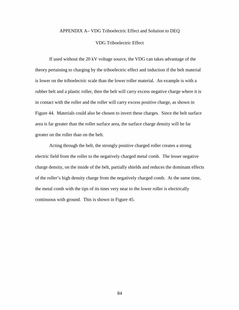
84
APPENDIX A– VDG Triboelectric Effect and Solution to DEQ
VDG Triboelectric Effect If used without the 20 kV voltage source, the VDG can takes advantage of the
theory pertaining to charging by the triboelectric effect and induction if the belt material
is lower on the triboelectric scale than the lower roller material. An example is with a
rubber belt and a plastic roller, then the belt will carry excess negative charge where it is
in contact with the roller and the roller will carry excess positive charge, as shown in
Figure 44. Materials could also be chosen to invert these charges. Since the belt surface
area is far greater than the roller surface area, the surface charge density will be far
greater on the roller than on the belt.
Acting through the belt, the strongly positive charged roller creates a strong
electric field from the roller to the negatively charged metal comb. The lesser negative
charge density, on the inside of the belt, partially shields and reduces the dominant effects
of the roller’s high density charge from the negatively charged comb. At the same time,
the metal comb with the tips of its tines very near to the lower roller is electrically
continuous with ground. This is shown in Figure 45.
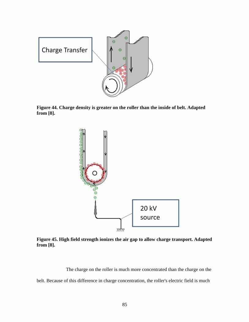
85
Figure 44. Charge density is greater on the roller than the inside of belt. Adapted from [8].
Figure 45. High field strength ionizes the air gap to allow charge transport. Adapted from [8].
The charge on the roller is much more concentrated than the charge on the
belt. Because of this difference in charge concentration, the roller's electric field is much

86
stronger than the belt's at the location of the roller and lower comb assembly. The strong
positive charge from the roller begins to do two things:
1. It attracts the electrons near the tips of the lower comb assembly. Metals are good
conductors because they are basically positive atoms surrounded by movable
electrons. The comb assembly has wire tips that are negatively charged because
the electrons have moved to the tips of the comb.
2. It begins to strip nearby air molecules of their electrons. The VDG now has free
electrons and positively charged atoms of air existing between the roller and the
comb. The electrons are attracted to the roller and repelled from the comb tips
while the positive atoms are repelled from the positively charged roller.
The negatively charged electrons from the air molecules are drawn toward the positively
charged roller, but the belt is in the way; therefore, the belt gets "coated" with the
negative charge, which it then carries away from the roller.
As long as there is air between the lower roller and comb assembly, the VDG will
continue to charge the belt. Theoretically, the VDG can continue to charge and is only
limited by the volume of the dome/capacitor.
As soon as electrons accumulate on the belt it is negatively charged. The
electrons now roll toward the upper roller and upper comb assembly. Since the upper
roller is made of a material that will repel the charge on the belt, and the upper comb
assembly is connected to the inside of the dome, the electrons on the belt move to the tips
of the metal comb as they are repelled by the now negatively charged top roller. Once
again the air breaks down between the comb and belt (just like the bottom roller), and the
positive atomic nuclei of air are attracted to the roller, and at the same time, the free

87
electrons in the air move to the comb. When a charged object touches the inside of the
metal container, the container accepts the charge, leaving the object neutral. The excess
charge then shows up on the outside surface of the dome, now making it a large
capacitor. It is through this effect that the VDG is able to achieve large voltage and
electric field.
Solutions to the RLC Differential Equation The MIL-STD-464 is a single pulse (with a fast rise time, and an order of
magnitude longer fall time), while the VDG gives an oscillating sinusoidal wave. To
better simulate a free field EMP pulse, the RLC circuit of the VDG needed to be
overdamped or critically damped. The solutions to the second-order linear differential
equation with constant coefficients, as outlined for the RLC circuit, are summarized in
Table 28 [18].
The RLC second order linear differential equation is given in its general form in Equation
(26):
2
2 0,d y dya b cydt dt
+ + = (26)
and has the characteristic equation of Equation (27).
2 0ar br c+ + = (27)

88
This characteristic equation is a quadratic formula and gives rise to three different
general solutions for the homogenous solution (yh) for the differential Equation (9).
These solutions depend on the value of the discriminate(∆ = 𝑏2 − 4𝑎𝑐), where b equals
R, α equals L, and c equals 1/C for the RLC circuit. The solutions to these equations
show that the overdamped or critically damped solutions are in the general form of MIL-
STD-464.
Since b equals the resistance R in the circuit, and it is squared, the resistance is
the dominant factor in determining the discriminator and whether the solution is
underdamped or overdamped. A comparison of these three different solutions is shown
in Figure 10 [18].
Table 28. Solution to the second-order linear differential equation with constant coefficients is shown. Adapted from [18].
Case 1 ∆ > 0
Real unequal roots:
𝑟1, 𝑟2 = −𝑏 ± √𝑏2 − 4𝑎𝑐
2𝑎
Over damped motion:
𝑦ℎ = 𝑐1𝑒𝑟1𝑡 + 𝑐2𝑒𝑟2𝑡 Case 2
∆= 0 Real repeated root:
𝑟 =−𝑏2𝑎
Critically damped motion:
𝑦ℎ = 𝑐1𝑒𝑟𝑡 + 𝑐2𝑡𝑒𝑟𝑡 Case 3
∆< 0 Complex conjugate roots:
𝑟1, 𝑟2 = 𝛼 ± 𝛽𝑖
𝛼 = 𝑏
2𝑎 , 𝛽 =
√4𝑎𝑐 − 𝑏2
2𝑎
Under damped motion:
𝑦ℎ = 𝑒𝛼𝑡(𝑐1𝑐𝑜𝑠𝛽𝑡 + 𝑐2𝑠𝑖𝑛𝛽𝑡)

89
APPENDIX B – Additional Equipment Confidence Experiments Equipment Confident Experiments:
The Signal source was connected straight into the oscilloscope with an RG 62/U
cable that was terminated with a 100 Ω shunt terminator. This data shows that with the
100 Ω shunt terminator VL is higher on the oscilloscope due to the fact that the 100 Ω
shunt terminator in parallel with the 93 Ω cable has a total impedance of 48 Ω, and a
constructive reflection is added to the VL.
Table 29. Voltage Load (VL) is higher when shunt terminators are used. This is because of constructive impedance reflections.
Signal Source
(50 Ω impedance)
Oscilloscope
(Terminated at 1MΩ) with RG-
62 (93 Ω) cable of 3ft length
Oscilloscope
(Terminated at 1M Ω) with RG-
62 (93 Ω) cable of 20 ft length
Frequency Voltage Frequency Voltage Frequency Voltage
1 MHz 1 V 1 MHz 1.33V 1 MHz 1.33V
1 MHz 5 V 1 MHz 6.68 V 1 MHz 6.60 V
1 MHz 10 V 1 MHz 13.44 V 1 MHz 13.36 V
1 MHz 5 V 1 MHz 6.68 V 1 MHz 6.60 V
10 MHz 5 V 10 MHz 6.72 V 10 MHz 6.72 V
15 MHz 5 V 15 MHz 6.88 V 15 MHz 6.52 V
20 MHz 5 V 20 MHz 6.96 V 20 MHz 6.56 V
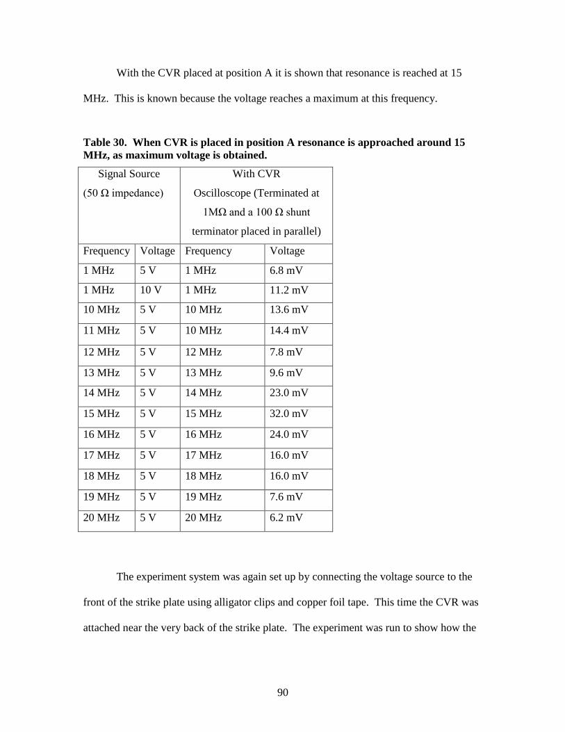
90
With the CVR placed at position A it is shown that resonance is reached at 15
MHz. This is known because the voltage reaches a maximum at this frequency.
Table 30. When CVR is placed in position A resonance is approached around 15 MHz, as maximum voltage is obtained.
Signal Source
(50 Ω impedance)
With CVR
Oscilloscope (Terminated at
1MΩ and a 100 Ω shunt
terminator placed in parallel)
Frequency Voltage Frequency Voltage
1 MHz 5 V 1 MHz 6.8 mV
1 MHz 10 V 1 MHz 11.2 mV
10 MHz 5 V 10 MHz 13.6 mV
11 MHz 5 V 10 MHz 14.4 mV
12 MHz 5 V 12 MHz 7.8 mV
13 MHz 5 V 13 MHz 9.6 mV
14 MHz 5 V 14 MHz 23.0 mV
15 MHz 5 V 15 MHz 32.0 mV
16 MHz 5 V 16 MHz 24.0 mV
17 MHz 5 V 17 MHz 16.0 mV
18 MHz 5 V 18 MHz 16.0 mV
19 MHz 5 V 19 MHz 7.6 mV
20 MHz 5 V 20 MHz 6.2 mV
The experiment system was again set up by connecting the voltage source to the
front of the strike plate using alligator clips and copper foil tape. This time the CVR was
attached near the very back of the strike plate. The experiment was run to show how the
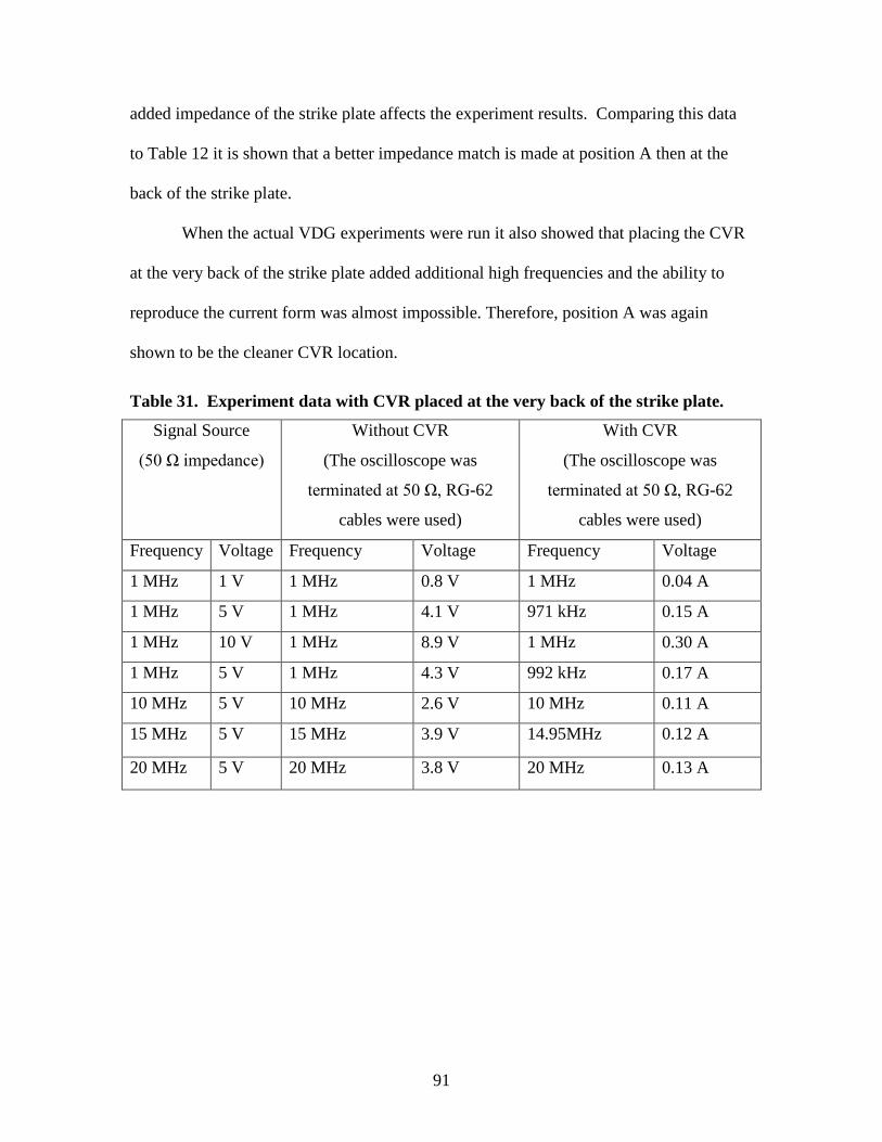
91
added impedance of the strike plate affects the experiment results. Comparing this data
to Table 12 it is shown that a better impedance match is made at position A then at the
back of the strike plate.
When the actual VDG experiments were run it also showed that placing the CVR
at the very back of the strike plate added additional high frequencies and the ability to
reproduce the current form was almost impossible. Therefore, position A was again
shown to be the cleaner CVR location.
Table 31. Experiment data with CVR placed at the very back of the strike plate.
Signal Source
(50 Ω impedance)
Without CVR
(The oscilloscope was
terminated at 50 Ω, RG-62
cables were used)
With CVR
(The oscilloscope was
terminated at 50 Ω, RG-62
cables were used)
Frequency Voltage Frequency Voltage Frequency Voltage
1 MHz 1 V 1 MHz 0.8 V 1 MHz 0.04 A
1 MHz 5 V 1 MHz 4.1 V 971 kHz 0.15 A
1 MHz 10 V 1 MHz 8.9 V 1 MHz 0.30 A
1 MHz 5 V 1 MHz 4.3 V 992 kHz 0.17 A
10 MHz 5 V 10 MHz 2.6 V 10 MHz 0.11 A
15 MHz 5 V 15 MHz 3.9 V 14.95MHz 0.12 A
20 MHz 5 V 20 MHz 3.8 V 20 MHz 0.13 A

92
APPENDIX C – Goodness of Fit and Computer Codes Goodness of Fit and Mathematical Algorithm and MATLAB Codes Used:
Goodness of Fit
Sum of Squares Due to Error:
This statistic measures the total deviation of the response values from the fit to
the response values. It is also called the summed square of residuals and is usually
labeled as SSE, as shown in Equation (28). A value closer to 0 indicates a better fit.
2
1( )
n
i i ii
SSE y yω=
= −∑ (28)
R-Square:
This statistic measures how successful the fit is in explaining the variation of the
data. Put another way, R-square is the square of the correlation between the response
values and the predicted response values. It is also called the square of the multiple
correlation coefficient and the coefficient of multiple determination.
R-square is defined as the ratio of the sum of squares of the regression (SSR) and the total
sum of squares (SST). SSR is defined in Equation (29).
2
1( )
n
i ii
SSR w y y=
= −∑ (29)
SST is also called the sum of squares about the mean, and is defined in Equation (30),
2
1( ) ,
n
i ii
SST y yω=
= −∑ (30)
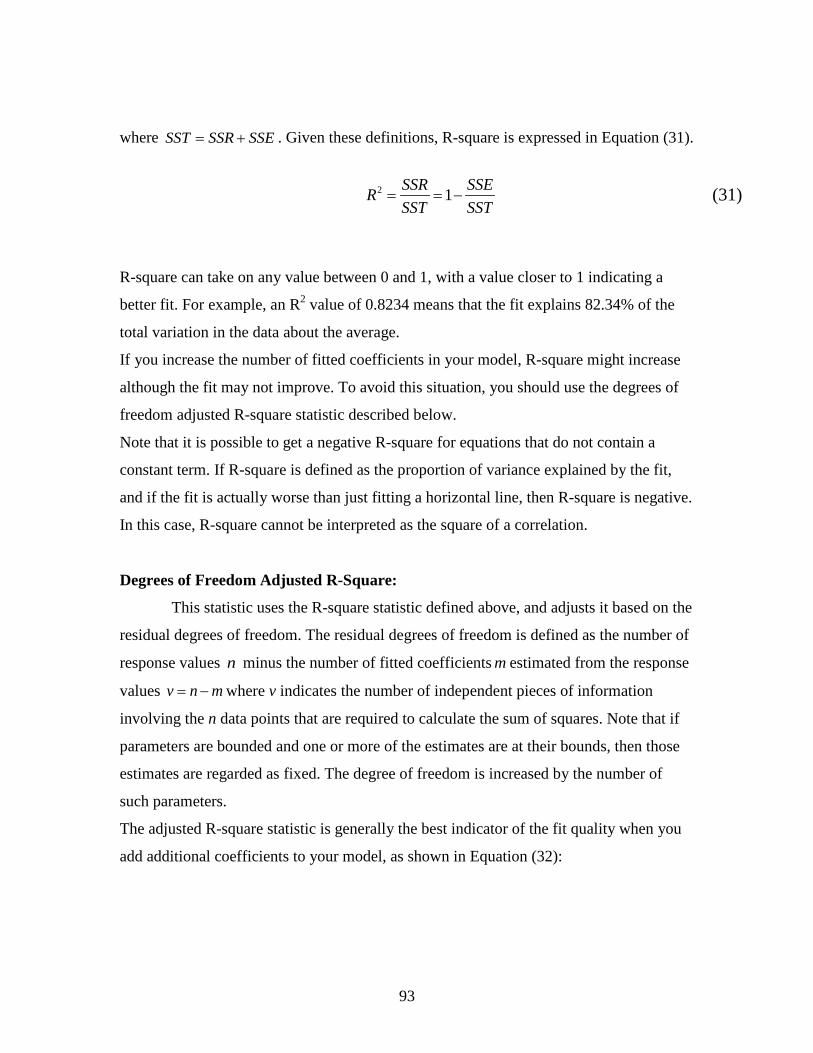
93
where SST SSR SSE= + . Given these definitions, R-square is expressed in Equation (31).
2 1SSR SSERSST SST
= = − (31)
R-square can take on any value between 0 and 1, with a value closer to 1 indicating a
better fit. For example, an R2 value of 0.8234 means that the fit explains 82.34% of the
total variation in the data about the average.
If you increase the number of fitted coefficients in your model, R-square might increase
although the fit may not improve. To avoid this situation, you should use the degrees of
freedom adjusted R-square statistic described below.
Note that it is possible to get a negative R-square for equations that do not contain a
constant term. If R-square is defined as the proportion of variance explained by the fit,
and if the fit is actually worse than just fitting a horizontal line, then R-square is negative.
In this case, R-square cannot be interpreted as the square of a correlation.
Degrees of Freedom Adjusted R-Square:
This statistic uses the R-square statistic defined above, and adjusts it based on the
residual degrees of freedom. The residual degrees of freedom is defined as the number of
response values n minus the number of fitted coefficients m estimated from the response
values v n m= − where v indicates the number of independent pieces of information
involving the n data points that are required to calculate the sum of squares. Note that if
parameters are bounded and one or more of the estimates are at their bounds, then those
estimates are regarded as fixed. The degree of freedom is increased by the number of
such parameters.
The adjusted R-square statistic is generally the best indicator of the fit quality when you
add additional coefficients to your model, as shown in Equation (32):
94
2 ( 1)adusted 1( 1)
SSE nRSST v
−= −
− (32)
The adjusted R-square statistic can take on any value less than or equal to 1, with a value
closer to 1 indicating a better fit.
Root Mean Squared Error:
This statistic is also known as the fit standard error and the standard error of the
regression, as shown in Equation (33),
RMSE s MSE= = , (33)
where MSE is the mean square error or the residual mean square, as shown in Equation
(34):
SSEMSEv
= (34)
A RMSE value closer to 0 indicates a better fit.
MATLAB Codes:
The Fast Fourier Transform (FFT) is an algorithm to compute the Discrete Fourier Transform (DFT) and its inverse. The MATLAB code used for this is shown: clear Data=importdata('File Name for data set.xls') X=Data(:,1); Y=Data(:,2);

95
dt=mean(diff(X)); nyquist=1/(2*dt); n=length(Y); freq=(1:n/2)./(n/2).*nyquist; ffty=fft(Y); ffty=abs(ffty.^2); plot(freq,ffty(1:length(Y)/2)) Computer model for the iterative time dependent spark gap current: close all clear all clc want_to_save=true; %Variable to Change --- Maybe dt=1e-11;% seconds - - time steps tmax=1e-6; % seconds - - time max inch = 3; % inches - - variable Spark Gap distance changes other variables c =200*10^(-12); %Farads 45 from Leahy's work L = 370e-9; %(1.4*10^(-9)/.03937)*(inch);%Henrys from Charlesworth Research ScaledAmplitude = 207; % from real data information to normalize from Spark Gap current to direct current t=0:dt:tmax; % time start at 0 to tmax l = (.0254/1)*(inch);% convertion of spark gap distance from inches to meters V0 = (2.9*10^(6)*(.0254/1)*(inch));% V/m (m) - - air breakdown voltage divided by Spark Gap distance to get voltage rho = 1.225 ;%kg/m^3 for 1 atmosphere before break down %% It=0; % initial conditions at time zero Itdt=1e-9; % initial conditions at time zero - - can not divide by zero jj=0; % initialize index h=waitbar(0); % to add the waitbar :) res=zeros(size(t)); % initializing the array with zeros to same size as t Itval=res; % initializing Itval - same as res Itdtval=res; % initializing Itval - same as res for tt=t % looping thru for steps of t jj=jj+1; waitbar(tt/tmax,h) Itdt=Itdt+It^(2/3)*dt; % approximation of the integral - - the smaller the dt the smaller the error but longer the time - for 45pF we max out at 1E-11

96
resistance=((7e-4*rho^(1/3)*l)./(Itdt)); % Spark Gap Resistance defined - - update for each iteration using the prevous iteration w0=sqrt(1/(L*c)-(resistance/(2*L))^2); % angular frequency defined It=V0/(w0*L)*exp(-resistance/(2*L)*tt)*sin(w0*tt); % Time dependent current defined res(jj)=resistance; % storing the array of resistance Itval(jj)=It; % storing the current array Itdtval(jj)=Itdt; % storing the integral values end close(h) % close the waitbar :) %% % Plots of the figurs - - each defined below Scaled_Output=figure(1); hold on plot(t,real(Itval)/max(real(Itval))*ScaledAmplitude,'r') % Scaled/normalized current set(gcf,'position',[644 676 560 420]) figure(5) plot(t,real(Itval)) % current set(gcf,'position',[50 676 560 420]) figure(2) loglog(t/1e-9,real(res)); % resistance set(gcf,'position',[1235 676 560 420]) figure(3) for ii=2:length(Itdtval) Integralerror(ii-1)=abs((Itdtval(ii)-Itdtval(ii-1))/Itdtval(ii)); end plot(Integralerror) set(gcf,'position',[50 99 560 420]) figure(4) plot(t,real(Itdtval)); % Current Integral for resistance set(gcf,'position',[644 99 560 420]) figure(1) if want_to_save uisave({'Itval','L','V0','c','dt','inch','l','rho','t'},'DataOut') end

97
Mathematica Codes The mathematica computer model used to manipulate data for a damped sin wave is shown:
Identify to Mathematica the directory where data are stored.
SetDirectory["L:\\Research\\ENP\\GNE Research\\EMP Research\\Kress\\MMA
Curve Fitting"];
Import data and remove the extra dimension generated by Mathematica.
plotData=Flatten[Import["16 Nov 2012 Full Pulse.xlsx","XLSX"],1];
Take a first look at the data.
dataPlot=ListPlot[plotData,JoinedTrue,PlotRangeAll,PlotStyleRed,AxesLab
el{Time[s], Current[A]}]
Now use the manipulate function to examine the data set. Start by guessing a
functional form, and plot the functional form over a range of fit parameters (Amplitude
and wave number).
Then, change the fit parameters to get the form to match the data set.
2. 107 4. 107 6. 107 8. 107 1. 106Times
200
100
100
200
CurrentA
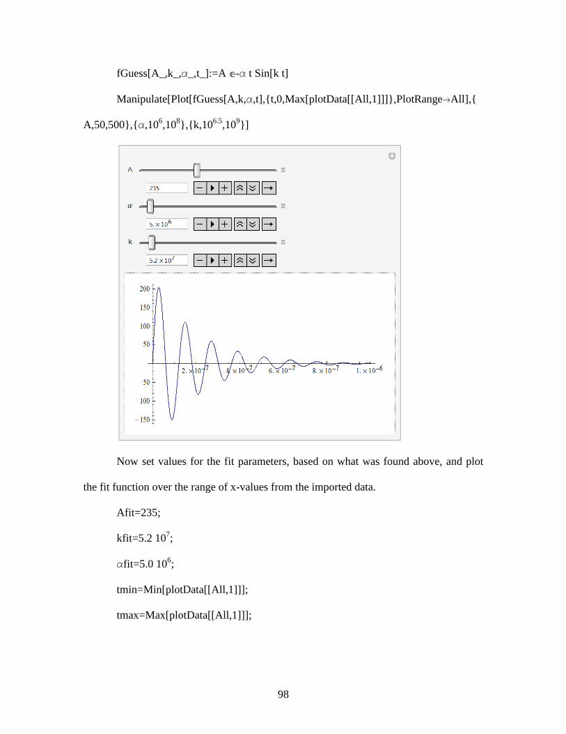
98
fGuess[A_,k_,_,t_]:=A - t Sin[k t]
Manipulate[Plot[fGuess[A,k,,t],{t,0,Max[plotData[[All,1]]]},PlotRangeAll],{
A,50,500},{,106,108},{k,106.5,109}]
Now set values for the fit parameters, based on what was found above, and plot
the fit function over the range of x-values from the imported data.
Afit=235;
kfit=5.2 107;
fit=5.0 106;
tmin=Min[plotData[[All,1]]];
tmax=Max[plotData[[All,1]]];
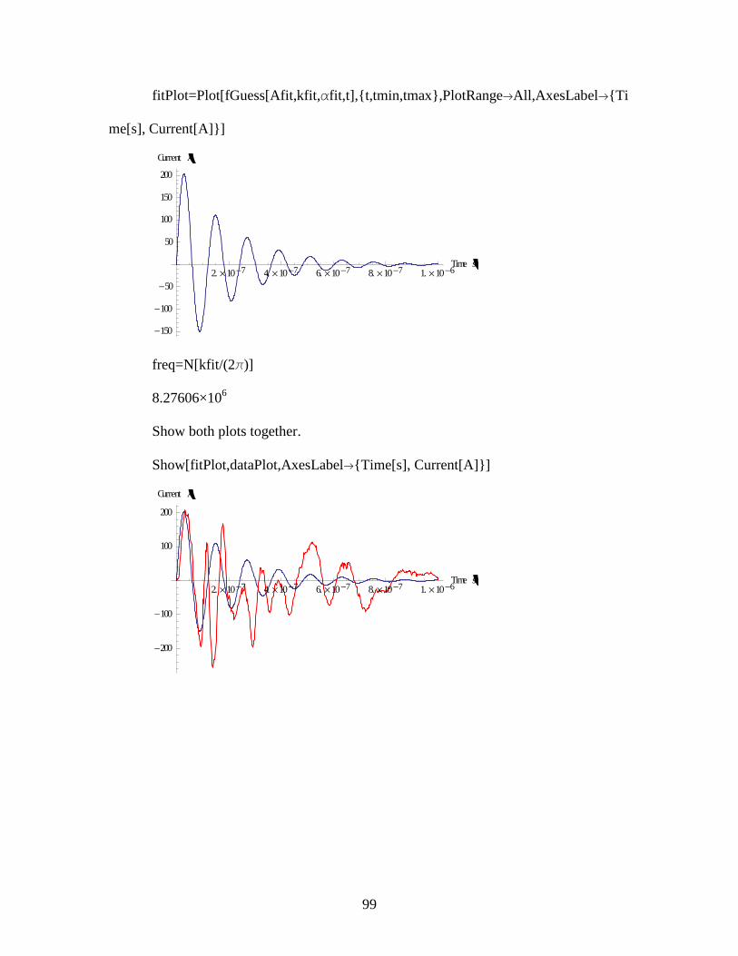
99
fitPlot=Plot[fGuess[Afit,kfit,fit,t],{t,tmin,tmax},PlotRangeAll,AxesLabel{Ti
me[s], Current[A]}]
freq=N[kfit/(2)]
8.27606×10⁶
Show both plots together.
Show[fitPlot,dataPlot,AxesLabel{Time[s], Current[A]}]
2. 107 4. 107 6. 107 8. 107 1. 106Times
150
100
50
50
100
150
200
CurrentA
2. 107 4. 107 6. 107 8. 107 1. 106Times
200
100
100
200
CurrentA

100
BIBLIOGRAPHY [1] Defense Threat Reduction Agency, High-Altitude Electromagnetic Pulse
(HEMP) Protection For Ground-Based C4I Facilities Performing Critical, Time-Urgent Missions Part 1 Fixed Facilities, Alexandria, VA: Department of Defense, 2005.
[2] J. c. Petrosky, Electromagnetic Pulse Effects Notebook SM2011, Dayton, OH: AFIT, 2011, p. 1.
[3] MIL-STD-464, Electromagnetic Environmental Effects Requirements for Systems, Wright-Patterson AFB: USAF/Aeronautical Systems Center, ASC/ENSI, 2530 Loop road West, Wright-Patterson AFB, OH 45433-7101, 1997.
[4] US Air Force Aeronautical Systems Center, Electromagnetic Environmental Effects Requirements for Systems Military Standard 464, Wright Patterson AFB, OH: US Department of Defense, 1997.
[5] T. Charlesworth and J. Staniforth, "Breakdown Experimetns in a Van De Graaff Generator," Nuclear Instrumetns and Methods, vol. 158, pp. 325-332, 1979.
[6] J. Leahy, Draft Thesis "Use of Van De Graaff for EMP Testing", Dayton, OH, 2011.
[7] P. A. Tipler and G. Mosca, Physics For Scientists and Engineers 6th Edition, NY: W.H. Feeman and Company, 2008.
[8] G. Images, "Triboelectric Effect," [Online]. Available: http://www.google.com/images. [Accessed 20 Nov 2012].
[9] C. J. Bridgman, Introduction To the PHysics of Neclear Weapons Effects, Wright-Patterson Air Force Base: U.S. Government, 2001.
[10] G. Cook, Interviewee, Air Force Research Laboratory Scientist. [Interview]. 18 February 2011.
[11] Weather Underground, "Weather Underground," 4 February 2010. [Online]. Available: http://www.wunderground.com/history/airport/KFFO/2010/2/4/DailyHistory.html?req_city=Fairborn&req_state=OH&. [Accessed 11 March 2011].
[12] J. Staniforth and T. Charlesworth, "Spark Channel Characteristics of a Large Van De Graaff Generator," Nuclear Instruments and Methods, vol. 188, pp. 483-489, 17 March 1981.
[13] J. Staniforth, "Voltage Calculation for a Single-Ended Van De Graaff Machine with Secondary Breakdowns," Nuclear Instruments and Methods, vol. 236, pp. 1-9, 7 April 1983.
[14] N. Engineering, "NESS Engineering Techinical Data RLC Circuit Formulas," [Online]. Available: http://www.nessengr.com/techdata/rlc/rlc.html#under. [Accessed 18 October 2012].

101
[15] G. L. Johnson, "Tesla Coil Impedance," in The First Tesla Museum and Science Center International Conference on Nikola Tesla, Farmingville, New York, 2006.
[16] T & M Research Products, "SERIES SDN-414 Current Viewing Resistors Description," [Online]. Available: http://www.tandmresearch.com/. [Accessed 6 April 2011].
[17] G. F. Knoll, Radiation Detection and Measurement - 4th ed., NJ: John Wiley & Sons, Inc, 2010.
[18] J. Farlow, J. E. Hall, J. M. McDill and B. H. West, Differential Equations & Linear Algebra, Upper Saddle river, NJ: Pearson Education, Inc., 2007.
[19] Wikipedia, "Wikipedia - Skin Effect," [Online]. Available: http://en.wikipedia.org/wiki/skin_effect. [Accessed 26 10 2012].

102
REPORT DOCUMENTATION PAGE Form Approved OMB No. 074-0188
The public reporting burden for this collection of information is estimated to average 1 hour per response, including the time for reviewing instructions, searching existing data sources, gathering and maintaining the data needed, and completing and reviewing the collection of information. Send comments regarding this burden estimate or any other aspect of the collection of information, including suggestions for reducing this burden to Department of Defense, Washington Headquarters Services, Directorate for Information Operations and Reports (0704-0188), 1215 Jefferson Davis Highway, Suite 1204, Arlington, VA 22202-4302. Respondents should be aware that notwithstanding any other provision of law, no person shall be subject to any penalty for failing to comply with a collection of information if it does not display a currently valid OMB control number. PLEASE DO NOT RETURN YOUR FORM TO THE ABOVE ADDRESS. 1. REPORT DATE (DD-MM-YYYY)
21 Mar 2013 2. REPORT TYPE Master’s Thesis
3. DATES COVERED (From – To) 28 Jun 2010 - 21 Mar 2013
4. TITLE AND SUBTITLE ANALYSIS OF A VAN DE GRAAFF GENERATOR FOR EMP DIRECT
CURRENT SURVIVABILITY TESTING
5a. CONTRACT NUMBER
5b. GRANT NUMBER 5c. PROGRAM ELEMENT NUMBER
6. AUTHOR(S) Kress, Robert J., LTC, USA
5d. PROJECT NUMBER
5e. TASK NUMBER
5f. WORK UNIT NUMBER
7. PERFORMING ORGANIZATION NAMES(S) AND ADDRESS(S) Air Force Institute of Technology Graduate School of Engineering and Management (AFIT/ENV) 2950 Hobson Way, Building 640 WPAFB OH 45433-8865
8. PERFORMING ORGANIZATION REPORT NUMBER AFIT-ENP-13-M-39
9. SPONSORING/MONITORING AGENCY NAME(S) AND ADDRESS(ES) Air Force Research Lab Dean Evans Program Lead, AFRL/RXPJ 2941 Hobson Way Wright-Patterson AFB, OH 45433 (937) 255-9135
10. SPONSOR/MONITOR’S ACRONYM(S) 11. SPONSOR/MONITOR’S REPORT NUMBER(S)
12. DISTRIBUTION/AVAILABILITY STATEMENT
13. SUPPLEMENTARY NOTES
14. ABSTRACT The direct current produced from the Van de Graaff (VDG) at the Air Force Research Laboratory (AFRL) has been measured and analyzed. The current pulse produced from the VDG is oscillatory. Experimental data show complete damping occurs after 8 oscillations and within 10-6 seconds. The spark gap distance and circuit resistance were varied to determine if the circuit could convert to an overdamped RLC circuit in order to reduce the oscillations. The data establishes that the VDG produces at least 3 full wave Fourier frequencies of: 3, 7, and 15 MHz ± 2.0 MHz, while the first oscillation had a measured mean frequencies of: 8.56 MHz ± 0.4 MHz for the 3″ spark gap distance; 6″ had a measured frequency of 13.95 MHz ± 1.0 MHz, and finally 7″ had a measured value of 15.78 MHz ± 1.3 MHz. The direct current amplitude of the first oscillation also rose as a function of spark gap distance from 202 ± 13.82 (A) at a spark gap of 3″ to 354 ± 22.10 (A) for a spark gap of 8″. Using the settings explored in this thesis, the VDG has some value for use in preliminary Electromagnetic Pulse (EMP) direct current testing, but further research is required in order for it to meet MIL-STD-464 validation criteria. 15. SUBJECT TERMS
Electromagnetic Pulse, Van de Graaff
16. SECURITY CLASSIFICATION OF: 17. LIMITATION OF ABSTRACT
UU
18. NUMBER OF PAGES
116
19a. NAME OF RESPONSIBLE PERSON
Dr. James C. Petrosky a. REPORT
U b. ABSTRACT
U c. THIS PAGE
U 19b. TELEPHONE NUMBER (Include area code) (937) 255-6565, x 4562 ([email protected])
Standard Form 298 (Rev. 8-98) Prescribed by ANSI Std. Z39-18