analysis of buck converters for on-chip integration with a ... · the target design point. full...
TRANSCRIPT

514 IEEE TRANSACTIONS ON VERY LARGE SCALE INTEGRATION (VLSI) SYSTEMS, VOL. 11, NO. 3, JUNE 2003
[7] , “On optimal board-level routing for FPGA-based logic emula-tion,” IEEE Trans. Computer-Aided Design, vol. 16, pp. 282–189, Mar.1997.
[8] S. Lin, Y. Lin, and T. Hwang, “Net assignment for the FPGA-based logicemulation system in the folded-clos network structure,”IEEE Trans.Computer-Aided Design, vol. 16, pp. 316–320, Mar. 1997.
[9] N. C. Chou, L. T. Liu, C. K. Cheng, W. J. Dai, and R. Lindelof, “Circuitpartitioning for huge logic emulation systems,” inProc. Design Automa-tion Conf., 1994, pp. 244–249.
[10] P. K. Chan and M. D. F. Schlag, “Architectural tradeoffs in field-pro-grammable-device based computing systems,” inProc. IEEE Workshopon FPGAs for Custom Computing Mach., Apr. 1993, pp. 152–161.
[11] M. Gokhale, W. Holmes, A. Kopser, S. Lucas, R. Minnich, and D.Sweely, “Building and using a highly parallel programmable logicarrays,”Comput., vol. 24, pp. 81–89, Jan. 1991.
[12] Y. Shang and B. W. Wah, “A Discrete lagrangian-based global-searchmethod for solving satisfiability problems,”J. Global Optim., vol. 12,no. 1, pp. 61–99, 1998.
[13] M. N. Velev, “Effective use of boolean satisfiability procedures in theformal verification of superscalar and VLIW microprocessors,” inProc.ACM/IEEE Design Automation Conf., Las Vegas, NV, June 18–22, 2001,pp. 226–231.
[14] M. W. Moskewicz, C. F. Madigan, Y. Zhou, L. Zhang, and S. Malik,“Chaff: Engineering an efficient SAT solver,” inProc. Design Automa-tion Conf., June 18–22, 2001, pp. 530–535.
[15] W. N. N. Hung, , http://www.ece.pdx.edu/~whung/BLRP, Aug. 2002.[16] R. G. Wood and R. A. Rutenbar, “FPGA routing and routability esti-
mation via Boolean satisfiability,”IEEE Trans. VLSI Syst., vol. 16, pp.222–231, June 1998.
Analysis of Buck Converters for On-Chip IntegrationWith a Dual Supply Voltage Microprocessor
Volkan Kursun, Siva G. Narendra, Vivek K. De, and Eby G. Friedman
Abstract—An analysis of an on-chip buck converter is presented in thispaper. A high switching frequency is the key design parameter that simulta-neously permits monolithic integration and high efficiency. A model of theparasitic impedances of a buck converter is developed. With this model, adesign space is determined that allows integration of active and passive de-vices on the same die for a target technology. An efficiency of 88.4% at aswitching frequency of 477 MHz is demonstrated for a voltage conversionfrom 1.2–0.9 volts while supplying 9.5 A average current. The area occupiedby the buck converter is 12.6 mm assuming an 80-nm CMOS technology.An estimate of the efficiency is shown to be within 2.4% of simulation atthe target design point. Full integration of a high-efficiency buck converteron the same die with a dual- microprocessor is demonstrated to befeasible.
Index Terms—Buck converter, dc-dc converter, dual supply voltage,high efficiency, integrated inductors, low power, low voltage, modeling ofdc–dc converters, monolithic dc–dc conversion, multiple supply voltages,power supply, supply voltage scaling, switching dc–dc converters, voltageregulator.
Manuscript received July 30, 2002; revised October 19, 2002. This work wassupported in part by a Grant from Intel Corporation.
V. Kursun and E. G. Friedman are with the Electrical and Computer Engi-neering Department, University of Rochester, Rochester, NY 14627-0231 USA.
S. G. Narendra and V. K. De are with the Microprocessor Research Labora-tories, Intel Corporation, Hillsboro, OR 97124 USA.
Digital Object Identifier 10.1109/TVLSI.2003.812289
I. INTRODUCTION
Decreasing the power dissipation and current demand of high-per-formance microprocessors are the two primary reasons for im-plementing a dual-VDD microprocessor [1]. Due to the quadraticdependence of the dynamic switching power and the more than lineardependence of the subthreshold and gate oxide leakage power onthe supply voltage, power dissipation is significantly reduced whenportions of a microprocessor operate at a lower voltage level. A linearrelationship exists between the current demand and power consump-tion of a microprocessor. Reducing the maximum power consumption,therefore, reduces the maximum current required by a microprocessor,thereby decreasing the number of power and ground pads on amicroprocessor die. In order to maximize this reduction in current,the lower voltage supply of a dual-VDD microprocessor should beintegrated on the same die with the microprocessor. Moreover, inorder to fully exploit expected reductions in power and current, theenergy overhead of an integrated dc–dc converter to produce a secondvoltage level must be minimized.
Buck converters are popular due to the high efficiency and goodoutput voltage regulation characteristics of these circuits [2]–[5]. Insingle power-supply microprocessors, the primary power supply is typ-ically an external (nonintegrated) buck converter. In a dual-VDD micro-processor, the choices are either a second external dc–dc converter, ora monolithic (both active and passive devices on the same die as theload) dc–dc converter.
In a typical nonintegrated switching dc–dc converter, significantenergy is dissipated by the parasitic impedances of the interconnectamong the nonintegrated devices (the filter inductor, filter capac-itor, power transistors, and pulse width modulation circuitry) [3].Moreover, the integrated active devices of a pulsewidth modulationcircuit are typically fabricated in an old technology with poor parasiticimpedance characteristics.
Integrating a dc–dc converter with a microprocessor can potentiallylower the parasitic losses as the interconnect between (and within) thedc–dc converter and the microprocessor is reduced. Additional energysavings can be realized by utilizing advanced deep submicrometer fab-rication technologies with lower parasitic impedances. The efficiencyattainable with a monolithic dc–dc converter, therefore, is higher thana nonintegrated dc–dc converter.
Fabrication of a monolithic switching dc–dc converter, however,imposes a challenge as the on-chip integration of inductive andcapacitive devices is required for energy storage and output signalfiltering. Integrated capacitors and inductors above certain values arenot acceptable due to the tight area constraints that exist within highperformance microprocessor integrated circuits (ICs). Another signif-icant issue with integrated inductors is the poor parasitic impedancecharacteristics which can degrade the efficiency of a voltage regulator.The value, physical size, and parasitic impedances of the passivedevices required to implement a buck converter, however, are reducedwith increasing switching frequency [2]–[4]. Integrated capacitors ofsmall value (used for decoupling and constrained by the available areaon the microprocessor die) are available in high-performance micro-processors [6]. Furthermore, with the use of magnetic materials, a newintegrated microinductor technology with relatively small parasiticimpedances and higher cutoff frequencies (over 3 GHz) has recentlybeen reported [7]. Therefore, employing switching frequencies higherthan the typical switching frequency range found in conventionaldc–dc converters permits the on-chip integration of active and passivedevices of a buck converter onto the same die as a high-performancemicroprocessor.
1063-8210/03$17.00 © 2003 IEEE

IEEE TRANSACTIONS ON VERY LARGE SCALE INTEGRATION (VLSI) SYSTEMS, VOL. 11, NO. 3, JUNE 2003 515
Fig. 1. Buck converter circuit.
The efficiency characteristics of a buck converter, however, changedramatically as the switching frequency is increased. The switchingfrequency of dc–dc converters has been, so far, limited to the rangefrom a few kilohertz to a few megahertz [2], [3]. Based on oversimpli-fied circuit models of switching dc–dc converters, a general assumptionin the research community has been that a high switching frequencydc–dc converter is not feasible with the expectation that the efficiencywould degrade significantly due to the increased power losses at highswitching frequencies [2], [3]. The low switching frequency range uti-lized in typical nonintegrated dc–dc converters has been a result of thisassumption rather than based on a study modeling the variation of thedc–dc converter efficiency as a function of the switching frequency.Comprehensive circuit models of the parasitic impedances of mono-lithic switching dc–dc converters are necessary in order to characterizean optimum circuit configuration with the maximum efficiency.
A parasitic model is presented in this paper to analyze the frequencydependent efficiency characteristics of a buck converter. A closed-formexpression that characterizes the power consumption of a monolithicbuck converter is proposed. The effects of scaling the active and pas-sive devices and the related switching and conduction losses on thetotal power characteristics of a buck converter are examined. With theproposed buck converter energy model, a design space which charac-terizes the integration of both active and passive devices on the samedie as a dual-VDD microprocessor while maintaining high efficiency isdetermined for an 80-nm CMOS technology. An efficiency of 88.4% isshown for a voltage conversion from 1.2 to 0.9 V while supplying 9.5 Amaximum current. The area of the buck converter at the target designpoint is 12.6 mm2 which is primarily occupied by a 100-nF filter ca-pacitor. Full integration of a high-efficiency buck converter on the samedie as a dual-VDD microprocessor is demonstrated to be feasible.
The basic operation of a buck converter is described in Section II.The proposed parasitic circuit model and a closed form expressionof the average power dissipation of a buck converter are presented inSection III. With the proposed analytic model, the efficiency charac-teristics of a buck converter are investigated in Section IV. Simulationresults at a target design point are presented in Section V. Finally, someconclusions are offered in Section VI.
II. OPERATION OF ABUCK CONVERTER
A buck converter is a standard switching dc–dc converter circuittopology with high efficiency and good output voltage regulation char-acteristics. Buck converters are used to generate a regulated dc outputsupply voltage from a higher (possibly nonregulated) dc input voltage.A typical buck converter circuit is shown in Fig. 1.
The operation of a buck converter circuit behaves in the followingmanner. The power MOSFETs, labeled asP1 andN1 in Fig. 1, pro-duce an ac signal at Node1 by a nonoverlapping switching action con-trolled by the pulse width modulator. The ac signal at Node1 is appliedto a second-order low-pass filter composed of an inductor and a capac-itor. The low-pass filter passes to the output the dc component of the acsignal at Node1. A small amount (assuming the filter corner frequencyis much smaller than the switching frequencyfs of the power MOS-FETs) of high-frequency harmonics generated by the switching actionof the power MOSFETs also reaches the output due to the nonidealcharacteristics of the output filter.
The buck converter output voltageVDD2(t) is [2]
VDD2(t) = VDD2 + Vripple(t) (1)
whereVDD2 is the dc component of the output voltage andVripple(t)is the voltage ripple waveform observed at the output due to the non-ideal characteristics of the output filter. The dc component of the outputvoltage is [2]
VDD2 =1
Ts
T
0
Vs(t)dt = DVDD1 (2)
whereVs(t) is the ac signal generated at Node1 andTs, D, andVDD1
are the period, duty cycle, and amplitude, respectively, ofVs(t). Asgiven by (2), any positive output dc voltage less thanVDD1 can begenerated by a buck converter by varying the duty cycleD.
The power transistors are typically large in physical size with a highparasitic capacitance. To control the operation of the power transis-tors, a series of MOSFET gate drivers are used. The driver buffers aretapered [8], [11] as shown in Fig. 1. The gate driver buffers are con-trolled by a pulse width modulator (PWM). Using a fast feedback cir-cuit, the PWM generates the necessary control signals for the power

516 IEEE TRANSACTIONS ON VERY LARGE SCALE INTEGRATION (VLSI) SYSTEMS, VOL. 11, NO. 3, JUNE 2003
MOSFETs such that a square wave with an appropriate duty cycle isproduced at Node1. During operation of the buck converter, the dutycycle and/or switching frequency are modified in order to maintain theoutput voltage at the desired value (output regulation) whenever vari-ations in the load current and input supply voltageVDD1 are detected.Due to the strong dependence of the output voltage on the switchingduty cycle [see (2)], precise output voltage regulation can be main-tained by a buck converter with a fast feedback circuit [2].
The inductor currentiL(t), output voltageVDD2(t), and capacitorcurrentiC(t)waveforms are shown in Fig. 2. The output voltage rippleis exaggerated in Fig. 2 for better illustration. The amplitude of theoutput voltage ripple�VDD2 is maintained at a small level (less than1%) as compared to the output dc voltageVDD2 in a typical buckconverter.
The filter capacitance is chosen such that the impedance of the ca-pacitor is much smaller than the load impedance. The ac component ofthe inductor current, therefore, passes through the filter capacitor whilethe dc componentI passes through the load (see Fig. 2). The outputvoltage increases while the filter capacitor is being charged when theinductor current rises aboveI . Similarly, the output voltage falls whilethe filter capacitor is being discharged when the inductor current de-creases belowI .
Expressions for the inductor current ripple�i and the amplitude ofthe output voltage ripple�VDD2 (see Fig. 2) are, respectively
�i =(VDD1 � VDD2)D
2Lfs(3)
�VDD2 =(VDD1 � VDD2)D
16LCfs2
=�i
8Cfs(4)
whereL is the filter inductance,C is the filter capacitance, andfs isthe switching frequency.
III. CIRCUIT MODEL OF A BUCK CONVERTER
A circuit model has been developed to analyze the frequency de-pendence of the efficiency characteristics of a buck converter. The pro-posed circuit model for the parasitic impedances of a buck converter isshown in Fig. 3.
The power consumption of a buck converter is a combination ofthe conduction losses caused by the parasitic resistive impedances andthe switching losses due to the parasitic capacitive impedances of thecircuit components. The power consumption of the pulse width mod-ulation feedback circuit is typically small as compared to the powerconsumption of the power train (the power MOSFETs, MOSFET gatedrivers, filter inductor, and filter capacitor) [2], [3], [5]. Only the powerdissipation of the power train components is, therefore, considered inthe efficiency analysis.
MOSFET related power losses are analyzed in Section III-A.An analysis of the filter inductor related losses is presented inSection III-B. The filter capacitor related losses are discussed inSection III-C. An analytical expression for the total buck converterpower dissipation is presented in Section III-D.
A. MOSFET Related Power Losses
The total power loss of a MOSFET is a combination of conductionlosses and dynamic switching losses. The conduction power is dissi-pated in the series resistance of the transistors operating in the activeregion. The dynamic power is dissipated each switching cycle whilecharging/discharging the gate oxide, gate-to-source/drain overlap, anddrain-to-body junction capacitances of the MOSFETs. In the followinganalysis it is assumed that the PWM control signals applied toP1andN1 are nonoverlapping. There is, therefore, no short-circuit cur-rent path throughP1 andN1 during the PWM signal transition. The
Fig. 2. Inductor currenti (t), output voltageV (t), and capacitor currenti (t) waveforms.
short-circuit power dissipated in the gate drivers is also neglected as-suming the transition times of the input signal applied at each powerMOSFET gate driver is smaller than the output transition times [3], [8],[11].
The average power consumption of a power MOSFET and the re-lated gate drivers is
PMOS =R0
Wi2rms +EWfs (5)
E �=�
�� 1(Cox + Cgs + 2Cgd + Cdb)V
2DD1 (6)
wherePMOS is the total power consumed during a switching cycle of apower MOSFET (which includes the power dissipated by the MOSFETgate drivers),R0 is the equivalent series resistance of a 1-�m-wide tran-sistor,irms is the rms current passing through the power MOSFET,W
is the width of the power MOSFET,� is the tapering factor of the powerMOSFET gate drivers,Cox, Cgs, Cgd, andCdb are the gate oxide,gate-to-source overlap, gate-to-drain overlap, and drain-to-body junc-tion capacitances, respectively, of a 1-�m-wide MOSFET, andE is theunit energy (per 1-�m-wide power MOSFET) consumed during a fullswitching cycle of a power MOSFET (includes the energy dissipatedin the gate drivers).
As given by (5), increasing the MOSFET transistor width reduces theconduction losses while increasing the switching losses. An optimumMOSFET width, therefore, exists that minimizes the total MOSFET re-lated power. The optimum MOSFET width and power loss expressionsfor a target rms current and switching frequency are
Wopt =R0i2rms
fsE(7)

IEEE TRANSACTIONS ON VERY LARGE SCALE INTEGRATION (VLSI) SYSTEMS, VOL. 11, NO. 3, JUNE 2003 517
Fig. 3. Circuit model of the parasitic impedances of a buck converter.
PMOS(min) =2 R0i2rmsfsE: (8)
As previously mentioned, it is assumed that the PWM signals for thepower MOSFETs are nonoverlapping. The time period during whichbothN1 andP1 are cutoff is called the dead time. The rms currentsthroughN1 andP1 (assuming a small dead time to switching period(Ts) ratio as compared toD) are
irms(NMOS) = (1�D) I2 +�i2
3(9)
irms(PMOS) = D I2 +�i2
3(10)
whereI is the dc current supplied to the load.Applying (8) forN1 andP1 and substituting the rms current expres-
sions (9) and (10), an expression for the total MOSFET related opti-mized power consumption of a buck converterPtot;MOS(opt) is
Ptot;MOS(opt) = a I2 +�i2
3fs (11)
a =2 R0NMOS(1�D)ENMOS
+pR0PMOSDEPMOS : (12)
B. Filter Inductor Related Power Losses
Some portion of the total energy consumption of a buck converteris due to the series resistance and the stray capacitance of the filterinductor. Integrated spiral inductors have a high series resistance andother intrinsic problems associated with a planar design, which makesthese inductors area inefficient [7]. Integration of a spiral inductor withsufficient inductance is, therefore, not feasible for a high-performancemicroprocessor. A novel low-resistance inductor has recently been re-ported [7]. Assuming the inductor parasitic impedances scale linearlywith the inductance [10], the total power dissipated in the filter inductoris
Ptot;inductor = bI2
�ifs+
�i
3fs+CL0V
2DD1
RL0�i(13)
b =(VDD1 � VDD2)DRL0
2(14)
whereCL0 andRL0 are, respectively, the parasitic stray capacitanceand parasitic series resistance per nanohenry inductance.
C. Filter Capacitor Related Power Losses
The filter capacitance affects the total power consumption of a buckconverter due to the effective series resistance (esr)RC . Assuming theintegrated capacitor is implemented utilizing the gate oxide capacitanceof a MOSFET, the total power dissipation of a filter capacitor is
Ptot;capacitor = dfs�i; (15)
d =8R0capLcapC0�VDD2
3(16)
where R0cap is the effective series resistance of a 1-�m-wideMOSFET,C0 is the gate oxide capacitance per�m2, andLcap is thechannel length of the MOSFET.
D. Total Power Consumption of a Buck Converter
Combining (11), (13), and (15), the total power consumption of abuck converter is
Pbuck = a I2 +�i2
3fs
+bI2
�ifs+
�i
3fs+CL0V
2DD1
RL0�i+ dfs�i (17)
wherea, b, andd are given by (12), (14), and (16), respectively.The power dissipation of a buck converter is a strong function of the
switching frequency and the inductor current ripple. As given by (17),a higher switching frequency increases the MOSFET and filter capac-itor related losses while decreasing the filter inductor related losses.Similarly, the MOSFET and filter capacitor power losses increase withgreater inductor current ripple. The relationship between the inductorlosses and the inductor current ripple however is more complicated. In-creased current ripple reduces the filter inductance required for a targetswitching frequency, which reduces the inductor parasitic impedances

518 IEEE TRANSACTIONS ON VERY LARGE SCALE INTEGRATION (VLSI) SYSTEMS, VOL. 11, NO. 3, JUNE 2003
and the related power loss. A higher current ripple, however, also in-creases the rms current through the filter inductor which causes theconduction losses of the inductor to be larger.
Depending upon the ratio of the inductor and MOSFET related com-ponents of the total power dissipation of a buck converter, the effi-ciency can actually increase with higher switching frequency and cur-rent ripple within a specified (fs, �i) range. This observation agreeswith the analysis presented in Section IV.
IV. EFFICIENCY ANALYSIS OF A BUCK CONVERTER
The efficiency of a buck converter is
� = 100�Pload
Pload + Pbuck
(18)
wherePload is the average power delivered to the load andPbuck is theaverage total internal power consumption of a buck converter as givenby (17).
The dc–dc converter efficiency is strongly dependent on theswitching frequencyfs. The switching frequency is, therefore, aprimary design variable in this analysis. Highfs is desirable fora monolithic buck converter due to the dependence of the filterinductance and capacitance onfs as described by (3) and (4). Asfsis increased, values ofL andC required to satisfy the target outputvoltage and current are reduced. Since the integration of the activeand passive devices of a buck converter circuit is a primary concern inthis analysis, a frequency range higher than the typical ranges foundin conventional buck converters is used throughout the analysis. Therange of switching frequencyfs is varied from 10 MHz–4 GHz.
As given by (17), another buck converter circuit parameter thatstrongly affects the circuit efficiency is the inductor current ripple�i.For a targetfs, increasing�i reduces the required filter inductance[see (3)]. The filter capacitance, however, must be increased to main-tain the output voltage ripple�VDD2 within acceptable limits withincreased�i for a targetfs [see (4)]. An appropriate�i, therefore,should be chosen that results in a filter inductance and capacitancesuitable for on-chip integration.
In the following analysis, it is assumed that the two power supplyvoltage levels used in the microprocessor are 1.2 volts(VDD1) and0.9 volts(VDD2). The average load current demandI is assumed tobe 9.5 A. It is also assumed that the tapering factor� of the powerMOSFET drivers is two for a worst case energy efficiency analysis. Itshould be noted that an optimal tapering factor of the power MOSFETgate drivers for energy efficiency is typically much greater thanthe tapering factor assumed in this analysis [11]. An 80-nm CMOStechnology is assumed. The global maximum efficiency circuit con-figuration is discussed in Section IV-A. The effect of a reduced filtercapacitance on the circuit configuration and the resulting efficiencycharacteristics of a buck converter are analyzed in Section IV-B.The allowable output voltage ripple�VDD2 is assumed to be 5 mVin Section IV-A and B. Another advantage of an integrated dc–dcconverter is that a higher�VDD2 is acceptable as compared to anonintegrated dc–dc converter, while satisfying the same load voltageand current specifications. The beneficial effects of increasing�VDD2
on the efficiency characteristics of a buck converter are examined inSection IV-C.
A. Circuit Analysis for Global Maximum Efficiency
The power dissipation and efficiency variation of a buck converterare shown in Fig. 4 for0:1 amperes� �i � 9:5 amperes and10 MHz � fs � 4 GHz. The “z” axis represents the power (in watts)and the efficiency (%) in Fig.4 (a) and (b), respectively. The MOSFET,filter inductor, and filter capacitor components of the total power
(a)
(b)
Fig. 4. Total power consumption and efficiency of a buck converter as afunction off and�i. (a) Total power (watts). (b) Efficiency (%).
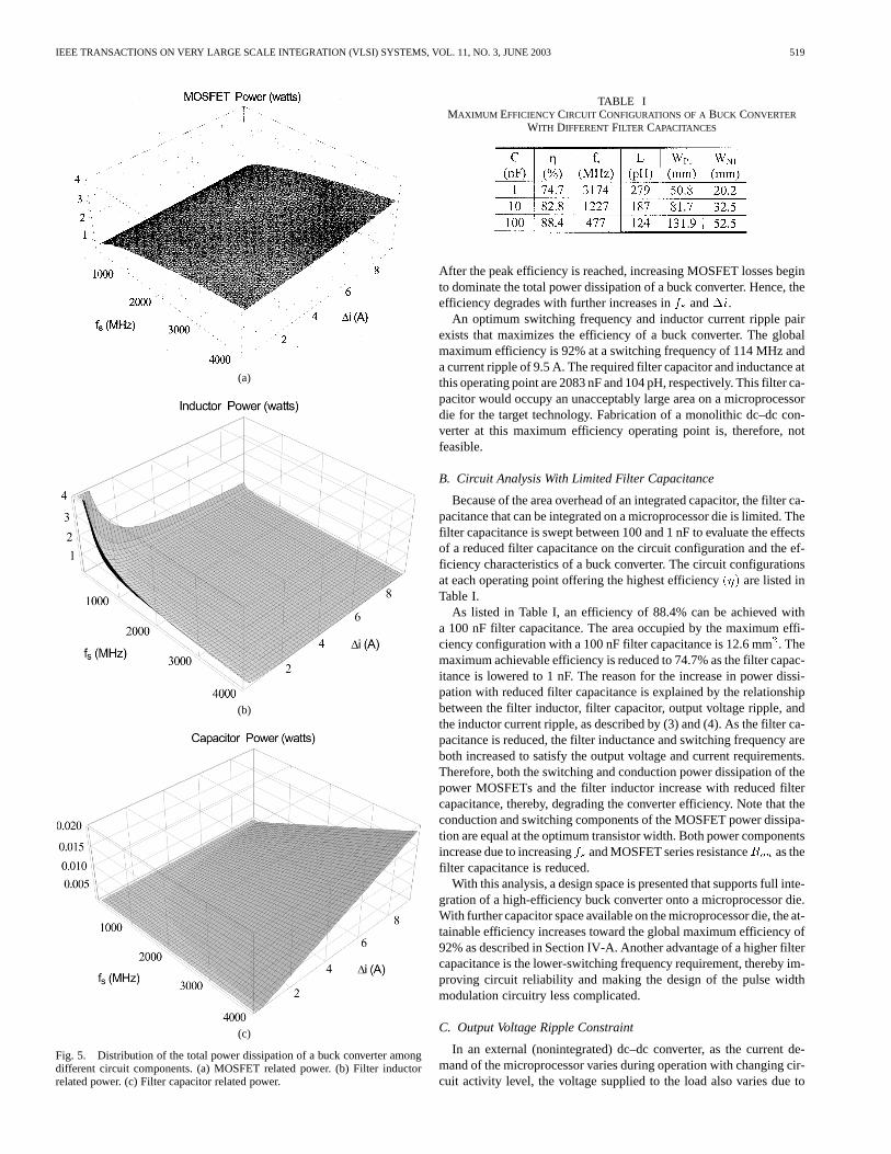
dissipation of a buck converter are shown in Fig. 5. The “z” axis inFig. 5 represents the power (in watts).
As shown in Fig. 5, the MOSFET and capacitor related powerincreases while the inductor power monotonically decreases withincreasing switching frequency and inductor current ripple. Thecapacitor power, however, is negligibly small (less than 1%) ascompared to the inductor and MOSFET power over the entire (fs,�i) range of analysis. The filter capacitor losses, although includedin the analysis are, therefore, not further discussed in the paper. Theefficiency of a buck converter is characterized by competing inductorand MOSFET losses. At lowfs and�i, the buck converter power isprimarily dissipated in the filter inductor. As the switching frequencyand current ripple are increased, the inductance is dramaticallyreduced, lowering the parasitic losses of the inductor. The MOSFETpower increases, however, with increasingfs and�i. At a certainrange offs and�i the inductor losses dominate the total losses. Asshown in Fig.4 (a), the total power dissipation of a buck converterdecreases with increasingfs and�i in the range dominated by theinductor losses.
IEEE TRANSACTIONS ON VERY LARGE SCALE INTEGRATION (VLSI) SYSTEMS, VOL. 11, NO. 3, JUNE 2003 519
(a)
(b)
(c)
Fig. 5. Distribution of the total power dissipation of a buck converter amongdifferent circuit components. (a) MOSFET related power. (b) Filter inductorrelated power. (c) Filter capacitor related power.
TABLE IMAXIMUM EFFICIENCY CIRCUIT CONFIGURATIONS OF ABUCK CONVERTER
WITH DIFFERENTFILTER CAPACITANCES
After the peak efficiency is reached, increasing MOSFET losses beginto dominate the total power dissipation of a buck converter. Hence, theefficiency degrades with further increases infs and�i.
An optimum switching frequency and inductor current ripple pairexists that maximizes the efficiency of a buck converter. The globalmaximum efficiency is 92% at a switching frequency of 114 MHz anda current ripple of 9.5 A. The required filter capacitor and inductance atthis operating point are 2083 nF and 104 pH, respectively. This filter ca-pacitor would occupy an unacceptably large area on a microprocessordie for the target technology. Fabrication of a monolithic dc–dc con-verter at this maximum efficiency operating point is, therefore, notfeasible.
B. Circuit Analysis With Limited Filter Capacitance
Because of the area overhead of an integrated capacitor, the filter ca-pacitance that can be integrated on a microprocessor die is limited. Thefilter capacitance is swept between 100 and 1 nF to evaluate the effectsof a reduced filter capacitance on the circuit configuration and the ef-ficiency characteristics of a buck converter. The circuit configurationsat each operating point offering the highest efficiency(�) are listed inTable I.
As listed in Table I, an efficiency of 88.4% can be achieved witha 100 nF filter capacitance. The area occupied by the maximum effi-ciency configuration with a 100 nF filter capacitance is 12.6 mm2. Themaximum achievable efficiency is reduced to 74.7% as the filter capac-itance is lowered to 1 nF. The reason for the increase in power dissi-pation with reduced filter capacitance is explained by the relationshipbetween the filter inductor, filter capacitor, output voltage ripple, andthe inductor current ripple, as described by (3) and (4). As the filter ca-pacitance is reduced, the filter inductance and switching frequency areboth increased to satisfy the output voltage and current requirements.Therefore, both the switching and conduction power dissipation of thepower MOSFETs and the filter inductor increase with reduced filtercapacitance, thereby, degrading the converter efficiency. Note that theconduction and switching components of the MOSFET power dissipa-tion are equal at the optimum transistor width. Both power componentsincrease due to increasingfs and MOSFET series resistanceRon as thefilter capacitance is reduced.
With this analysis, a design space is presented that supports full inte-gration of a high-efficiency buck converter onto a microprocessor die.With further capacitor space available on the microprocessor die, the at-tainable efficiency increases toward the global maximum efficiency of92% as described in Section IV-A. Another advantage of a higher filtercapacitance is the lower-switching frequency requirement, thereby im-proving circuit reliability and making the design of the pulse widthmodulation circuitry less complicated.
C. Output Voltage Ripple Constraint
In an external (nonintegrated) dc–dc converter, as the current de-mand of the microprocessor varies during operation with changing cir-cuit activity level, the voltage supplied to the load also varies due to
520 IEEE TRANSACTIONS ON VERY LARGE SCALE INTEGRATION (VLSI) SYSTEMS, VOL. 11, NO. 3, JUNE 2003
(a) (b)
(c) (d)
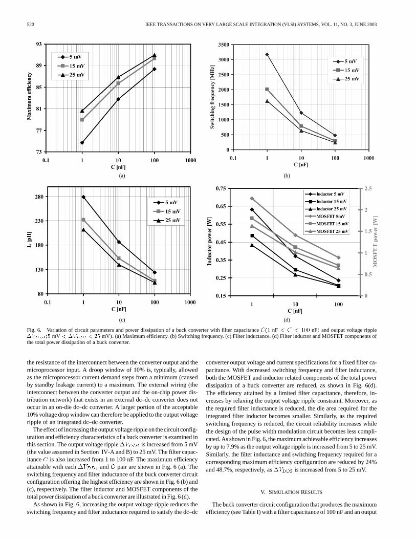
Fig. 6. Variation of circuit parameters and power dissipation of a buck converter with filter capacitanceC(1 nF < C < 100 nF) and output voltage ripple�V (5 mV < �V < 25 mV). (a) Maximum efficiency. (b) Switching frequency. (c) Filter inductance. (d) Filter inductor and MOSFET components ofthe total power dissipation of a buck converter.
the resistance of the interconnect between the converter output and themicroprocessor input. A droop window of 10% is, typically, allowedas the microprocessor current demand steps from a minimum (causedby standby leakage current) to a maximum. The external wiring (theinterconnect between the converter output and the on-chip power dis-tribution network) that exists in an external dc–dc converter does notoccur in an on-die dc–dc converter. A larger portion of the acceptable10% voltage drop window can therefore be applied to the output voltageripple of an integrated dc–dc converter.
Theeffect of increasing the output voltage ripple on thecircuit config-uration and efficiency characteristics of a buck converter is examined inthis section. The output voltage ripple�VDD2 is increased from 5 mV(the value assumed in Section IV-A and B) to 25 mV. The filter capac-itanceC is also increased from 1 to 100 nF. The maximum efficiencyattainable with each�VDD2 andC pair are shown in Fig. 6 (a). Theswitching frequency and filter inductance of the buck converter circuitconfiguration offering the highest efficiency are shown in Fig. 6 (b) and(c), respectively. The filter inductor and MOSFET components of thetotal power dissipation of a buck converter are illustrated in Fig. 6 (d).
As shown in Fig. 6, increasing the output voltage ripple reduces theswitching frequency and filter inductance required to satisfy the dc–dc
converter output voltage and current specifications for a fixed filter ca-pacitance. With decreased switching frequency and filter inductance,both the MOSFET and inductor related components of the total powerdissipation of a buck converter are reduced, as shown in Fig. 6(d).The efficiency attained by a limited filter capacitance, therefore, in-creases by relaxing the output voltage ripple constraint. Moreover, asthe required filter inductance is reduced, the die area required for theintegrated filter inductor becomes smaller. Similarly, as the requiredswitching frequency is reduced, the circuit reliability increases whilethe design of the pulse width modulation circuit becomes less compli-cated. As shown in Fig. 6, the maximum achievable efficiency increasesby up to 7.9% as the output voltage ripple is increased from 5 to 25 mV.Similarly, the filter inductance and switching frequency required for acorresponding maximum efficiency configuration are reduced by 24%and 48.7%, respectively, as�VDD2 is increased from 5 to 25 mV.
V. SIMULATION RESULTS
The buck converter circuit configuration that produces the maximumefficiency (see Table I) with a filter capacitance of 100 nF and an output
IEEE TRANSACTIONS ON VERY LARGE SCALE INTEGRATION (VLSI) SYSTEMS, VOL. 11, NO. 3, JUNE 2003 521
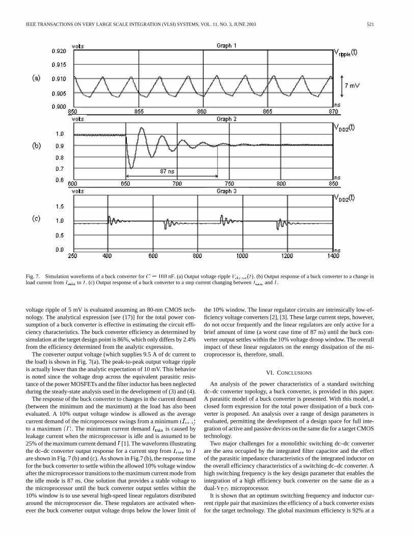
Fig. 7. Simulation waveforms of a buck converter forC = 100 nF. (a) Output voltage rippleV (t). (b) Output response of a buck converter to a change inload current fromI to I . (c) Output response of a buck converter to a step current changing betweenI andI .
voltage ripple of 5 mV is evaluated assuming an 80-nm CMOS tech-nology. The analytical expression [see (17)] for the total power con-sumption of a buck converter is effective in estimating the circuit effi-ciency characteristics. The buck converter efficiency as determined bysimulation at the target design point is 86%, which only differs by 2.4%from the efficiency determined from the analytic expression.
The converter output voltage (which supplies 9.5 A of dc current tothe load) is shown in Fig. 7(a). The peak-to-peak output voltage rippleis actually lower than the analytic expectation of 10 mV. This behavioris noted since the voltage drop across the equivalent parasitic resis-tance of the power MOSFETs and the filter inductor has been neglectedduring the steady-state analysis used in the development of (3) and (4).
The response of the buck converter to changes in the current demand(between the minimum and the maximum) at the load has also beenevaluated. A 10% output voltage window is allowed as the averagecurrent demand of the microprocessor swings from a minimum(Imin)to a maximum(I). The minimum current demandImin is caused byleakage current when the microprocessor is idle and is assumed to be25% of the maximum current demandI [1]. The waveforms illustratingthe dc–dc converter output response for a current step fromImin to I
are shown in Fig. 7 (b) and (c). As shown in Fig.7 (b), the response timefor the buck converter to settle within the allowed 10% voltage windowafter the microprocessor transitions to the maximum current mode fromthe idle mode is 87 ns. One solution that provides a stable voltage tothe microprocessor until the buck converter output settles within the10% window is to use several high-speed linear regulators distributedaround the microprocessor die. These regulators are activated when-ever the buck converter output voltage drops below the lower limit of
the 10% window. The linear regulator circuits are intrinsically low-ef-ficiency voltage converters [2], [3]. These large current steps, however,do not occur frequently and the linear regulators are only active for abrief amount of time (a worst case time of 87 ns) until the buck con-verter output settles within the 10% voltage droop window. The overallimpact of these linear regulators on the energy dissipation of the mi-croprocessor is, therefore, small.
VI. CONCLUSIONS
An analysis of the power characteristics of a standard switchingdc–dc converter topology, a buck converter, is provided in this paper.A parasitic model of a buck converter is presented. With this model, aclosed form expression for the total power dissipation of a buck con-verter is proposed. An analysis over a range of design parameters isevaluated, permitting the development of a design space for full inte-gration of active and passive devices on the same die for a target CMOStechnology.
Two major challenges for a monolithic switching dc–dc converterare the area occupied by the integrated filter capacitor and the effectof the parasitic impedance characteristics of the integrated inductor onthe overall efficiency characteristics of a switching dc–dc converter. Ahigh switching frequency is the key design parameter that enables theintegration of a high efficiency buck converter on the same die as adual-VDD microprocessor.
It is shown that an optimum switching frequency and inductor cur-rent ripple pair that maximizes the efficiency of a buck converter existsfor the target technology. The global maximum efficiency is 92% at a

522 IEEE TRANSACTIONS ON VERY LARGE SCALE INTEGRATION (VLSI) SYSTEMS, VOL. 11, NO. 3, JUNE 2003
switching frequency of 114 MHz and a current ripple of 9.5 A assumingan 80-nm CMOS technology. The required filter capacitance and in-ductance at this operating point are 2083 nF and 104 pH, respectively.
The effects of reducing the filter capacitance due to the tight areaconstraints on a microprocessor die have been examined. An efficiencyof 88.4% is shown at a switching frequency of 477 MHz with a filtercapacitance of 100 nF. The area occupied by the buck converter is12.6 mm2 and is dominated by the area of the integrated filter capac-itance. The analytic model for the converter efficiency is within 2.4%of the simulation results at the target design point.
The output voltage ripple can be increased in a fully integrated dc–dcconverter, offering the same 10% output voltage droop window as com-pared to a nonintegrated dc–dc converter. It is shown that the maximumattainable efficiency increases by up to 7.9% as the output voltageripple is increased from 5 to 25 mV. Similarly, the filter inductance andswitching frequency required for maximizing the efficiency of a buckconverter are reduced by 24% and 48.7%, respectively, with increasing�VDD2.
ACKNOWLEDGMENT
The authors would like to thank D. Gardner and P. Kumar of IntelCorporation for their contributions to this work. The authors would alsolike to thank the reviewers for their comments and suggestions.
REFERENCES
[1] S. Borkar, “Low power design challenges for the decade,” inProc.IEEE/ACM Design Automation Conf., June 2001, pp. 293–296.
[2] R. W. Erickson and D. Maksimovic,Fundamentals of Power Elec-tronics. Norwell, MA: Kluwer, 2001.
[3] A. P. Chandrakasan and R. W. Brodersen,Low-Power CMOS DigitalDesign. Norwell, MA: Kluwer, 1995.
[4] S. K. Reynolds, “A DC-DC converter for short-channel CMOS tech-nologies,”IEEE J. Solid-State Circuits, vol. 32, pp. 111–113, Jan. 1997.
[5] A. Stratakos, S. R. Sanders, and R. W. Brodersen, “A low-voltage CMOSDC-DC converter for a portable battery-operated system,” inProc. IEEEPower Electron. Specialists Conf., Apr. 1994, pp. 619–626.
[6] P. E. Gronowskiet al., “High-performance microprocessor design,”IEEE J. Solid-State Circuits, vol. 33, pp. 676–686, May 1998.
[7] D. Gardner, A. M. Crawford, and S. Wang, “High frequency (GHz) andlow resistance integrated inductors using magnetic materials,” inProc.IEEE Int. Interconnect Technol. Conf., June 2001, pp. 101–103.
[8] B. S. Cherkauer and E. G. Friedman, “A unified design methodologyfor CMOS tapered buffers,”IEEE Trans. VLSI Syst., vol. 3, pp. 99–111,Mar. 1995.
[9] H. J. M. Veendrick, “Short-circuit dissipation of static CMOS circuitryand its impact on the design of buffer circuits,”IEEE J. Solid-State Cir-cuits, vol. SC-19, pp. 468–473, Aug. 1984.
[10] D. Gardner, Intel Corp., Components Res., Santa Clara, CA, privatecommunication, 2001.
[11] V. Kursun, S. G. Narenda, V. K. De, and E. G. Friedman, “MonolithicDC-DC Converter Analysis and MOSFET Gate Voltage Optimization,”in Proc. IEEE Int. Symp. on Quality Electron. Design, Mar. 2003, pp.279–284.