analytical procedures for portable lead ......alloys, (2) aiding in alloy acceptability...
TRANSCRIPT
IPC SOLDER PRODUCTS VALUE COUNCIL LEAD-FREE TECHNICAL WHITE PAPER
ANALYTICAL PROCEDURES FOR PORTABLE LEAD-FREE ALLOY TEST DATA
May, 2010
®
Association Connecting Electronics Industries

®
Association Connecting Electronics Industries
2
AIM
Amtech, Inc.
Cookson Electronics
Henkel Corporation
Heraeus, Inc.
Indium Corporation
Inventec Performance Chemicals
Kester
Koki Company Ltd.
Matsumura Metal Co., Ltd.
Metallic Resources, Inc.
Nihon Superior Company Ltd.
Nordson EFD LLC
P. Kay Metal Inc.
Qualitek
Redring Solder
Redring Solder (M) SDN
Senju Metal Industry
Shenmao Technology, Inc.
Sigma Ming GOA Electronics
Yik Shing Tat industrial Co.
In support of IPC’s Mission Statement, IPC solder manufacturers recognize that the PWB and electronics assembly industries, comprised of the entire supply chain, must grow profitably. The
Solder Products Value Council Steering Committee’s objective is to identify and execute programs designed to enhance the competitive position of solder manufacturers and their customers.
SOLDER PRODUCTS VALUE COUNCIL MEMBERS
MISSION STATEMENT

®
Association Connecting Electronics Industries
3
IPC SOLDER PRODUCTS VALUE COUNCIL LEAD-FREE TEChNICAL whITE PAPERAnalytical Procedures for Portable Lead Free Alloy Test Data
1.1 Scope This document prescribes general requirements for determining critical physical and mechanical properties of bulk lead-free solder alloys used to make high quality electronic interconnections. This document describes material tests that generate portable data for: (1) direct comparison of different alloys, (2) aiding in alloy acceptability determination for various applications, (3) development of reliability models, and (4) other uses.
1.1.1 Purpose This standard defines the characteristics of solder alloys through the definitions of properties and specification of test methods. These requirements for solder alloys are defined in general terms of material properties. In practice, where more stringent requirements are necessary, additional requirements shall be defined by mutual agreement between the user and supplier. Users are cautioned to perform other tests (beyond the scope of this specification) to fully determine the acceptability of solder alloys for specific purposes.
IntroductionDue to marketing and legislative pressures in Asia and Europe, the electronics industry has moved to adopt lead-free solders. These lead-free materials are considered by some to be environmentally preferable to lead containing solders that dominated electronics manufacturing for many years.
Although the issue as to whether lead-free solders are indeed environmentally preferred compared to lead containing solders is still under debate, market and legislative actions have forced a change in materials used in electronics assembly.
Accordingly, solder material suppliers are being asked to provide the electronics industry with solders that are lead free (per the accepted technical definition of that term) and yet still provide all the needed properties – including ease of assembly and reliability – properties the electronics industry has come to expect from lead containing solders. Accordingly solder suppliers are devoting their efforts to improve their products and offer their customers an ever growing choice of alloys.
However, for OEMs and EMS companies this proliferation of alloy choices poses a problem. There isn’t the wealth of physical data available for these alloys as there is for 63/37 (tin/lead) because of limited time in the market and the limited years of investigation by suppliers, users and academia.
Many of the first lead-free alloys introduced, e.g. SAC 305, are, if not completely characterized, their reliability properties are better understood than the new alloys being introduced – making it difficult to compare alloy properties. So while it is tempting for the electronics assembly industry to look to the new alloys as solutions to the manufacturing issues of the “older” materials, the lack of reliability characterization of these new materials introduces an element of uncertainty when compared to current lead free solders.
To address this problem, the IPC Solder Products Value Council (IPC SPVC) in cooperation with several leading OEMs and EMS providers has developed a set of test protocols for evaluation of new lead free alloys on the basis of their physical properties, e.g. creep, and their performance in the assembly of a standardized test vehicle.
This paper will focus on the physical testing of lead-free alloys. The goal of this white paper is to reduce the time and effort required to characterize an alloy and thus help the electronics assembly industry improve their assembly processes without jeopardizing reliability.
Test Subcommittee MembersThe work of the SPVC in this study was under the direction of four team members chosen from the SPVC include Paul Lotosky, Cookson Electronics; Ross Bernstein, Indium; Stan Rothschild, Metallic Resources and Karl Seelig, AIM. Greg Munie of IPC was appointed to be the secretary for the team.
Acknowledgements This effort could not have been achieved without the support of numerous people in the industry. SPVC would like to specifically acknowledge the efforts of:
1.0 SCOPE
Dennis Fritz, MacDermid, Inc.Carol Handwerker, Purdue University Greg Henshall, Hewlett-Packard CompanyDavid Hillman, Rockwell CollinsDavid Humphrey, Honeywell Engines & SystemsChristopher Hunt, National Physical LaboratoryWayne Johnson, Auburn UniversityStephan Meschter, BAE Systems Platform SolutionsJennifer Nguyen, Flextronics InternationalAnthony Rafanelli, Raytheon CompanyDongkai Shangguan, Flextronics InternationalJoseph Smetana, Alcatel-LucentGanesh Subbarayan, Purdue UniversityFred Verdi, ACI/EMPFPaul Vianco Sandia, National Labs AlbuquerqueGeorge Wenger, Andrew CorporationThomas Woodrow, Boeing CompanyLinda Woody, Lockheed Martin Missile & Fire ControlDongji Xie, Flextronics International
®
Association Connecting Electronics Industries
4
3.1 General Requirements3.1 .1 Conflict In the event of conflict between the requirements of this specification and those of the applicable procurement documents, the following order of precedence applies:
1. The applicable procurement document2. The applicable specification sheet/drawing3. This standard4. Applicable referenced documents (see paragraph 2.0)
3.1 .2 Terms and Definitions Definitions applicable to this specification shall conform to IPC-T-50, J-STD-001, J-STD-002, J-STD-006 and as follows. The terms and definitions are in accordance with IPC-T-50.
3.2 Description of the Alloy 3.2.1 Alloy Composition The percentage of each element in an alloy shall be determined by any standard analytical procedure. Wet chemistry shall be used as the reference procedure only as needed. It should be noted that many new alloys may have proprietary elements added that are not noted in the technical literature of the manufacturer; the percentage of such elements shall be reported. To provide a full compositional assessment, including dopants, a general element analysis method such as Atomic Emission Spectroscopy/Inductively Coupled Plasma (AES/ICP or arc/spark) method of generating a complete elemental spectrum shall be used. Testing by X-ray fluorescence (XRF) shall not be used because it is not sufficiently accurate.
3.3 Differential Scanning Calorimetry The method followed shall be ASTM E794-01, Standard Test Method for Melting and Crystallization Temperatures by Thermal Analysis at ramp rates of 2°C and 10°C to provide complete information on liquidus and solidus temperatures, pasty range and any phase transitions that may occur. To condition the pan and alloy sample, a pre-conditioning sweep from ambient to 50°C above the liquidus temperature of the alloy shall be performed before actual data collection. The collection of data is to be done in a second ramp conducted after the sample returns to ambient temperature. Data shall be reported in the form of a standard curve of heat flow versus temperature, where temperature ranges from ambient to 50°C above the liquidus point of the alloy. In all cases, standard curves of pure indium and zinc metals are to be provided as reference and control.
3.4 wetting Balance Testing Wetting balance testing shall be conducted per the method described in J-STD-002B Solderability Tests for Component Leads, Terminations, Lugs, Terminals and wires. Data shall be reported as wetting curves of the alloy on standard finish described below or on finishes of interest to the user, e.g. OSP copper. Temperatures of testing and geometry of the test specimen are described in sections 3.4.1. through 3.4.4. Other testing conditions, e.g. parallel plate wetting, are to be negotiated between vendor and user.
The following documents of the issue currently in effect, form a part of this specification to the extent specified herein.
2.1 Joint Standards1
J-STD-001 Soldering requirements for Electronic Interconnections (Supersedes IPC-S-8 15)
J-STD-002B Solderability Tests for Component Leads, Terminations, Lugs, Terminals and Wires
J-STD-006 Requirements for Alloys and Solder Products
2.2 International Standards Organization2
ISO 9001 Quality Systems — Model for Quality Assurance in Design, Development, Production, Installation and Servicing.
ISO 9002 Quality Systems — Model for Quality Assurance in Production, Installation and Servicing.
2.3 IPC1
IPC-T-50 Terms and Definitions for Interconnecting and Packaging Electronic Circuits
IPC-TM-650 Test Methods Manual
2.4 NIST NIST Special Publication 960-8 Test Procedures for Developing Solder Data3
1 Application for copies should be addressed to the IPC, 3000 Lakeside Drive, Suite 309S, Bannockburn, Illinois 60015-1219
2 Publications are available from the International Standards Organization 1 Rue de Varembe, Case 56, CH-1211 Geneve 20 Switzerland
3 http://www.boulder.nist.gov/div853/Publication%20files/NIST_Solder_Practice_Guide_960.pdf
3.0 REQUIREMENTS
2.0 APPLICABLE DOCUMENTS

®
Association Connecting Electronics Industries
5
3.4.1 Test Materials • Testcouponsshallbeplatedthrough-holecouponsasillustrated
in Figure 4-8 of J-STD-003 • Thesurfacefinishshallbebarecopperunlessotherwiseagreed
on by user and supplier. • PCBthickness:0.062in• Laminate:Isola406• Layercount:4• Performthetestfortensamplesofthenewalloy,aswellasten
samples of the control SAC 3053.4. 2 Test Vehicle Assembly 3.4.2.1 Constants • Flux:standardactivatedrosinflux#2forPb-freealloys• Pottemperature:255°C,accordingtothestandardforPb-free
alloys3.4.2.2 Assumptions • Thepottemperaturemustbevalidatedbyathermocouplefor
each run• Providecontaminationreportsbeforeandaftertestforboththe
new alloy and SAC 305 control3.4.3 wetting Test Method • Precondition: - 8 hours at 72°C/85% humidity - Followed by 1 hour bake at 105°C • Testconditions:Partsimmersedat45°incidenttosolderpotto
a depth of 0.4 mm at 2 mm/sec3.4.4 Test Report The test report shall provide wetting balance curves showing the ten individual coupon results (not averaged) for each alloy, following the suggested criteria from J-STD-003.
3.5 Copper Dissolution Copper dissolution shall be determined per NIST Special Publication 960-8, Section 13, “Liquid Solder Dissolution.”
3.6. Thermal Expansion, Tensile and Creep Testing. This testing is intended to provide the information needed to model the physical properties of the alloy and to provide information that could help in evaluating acceptability of alloys for specific purposes. (The user of this document is referred to NIST Special Publication 960-8, Test Procedures for Developing Solder Data, for additional information on these types of test procedures.)
3.6.1 Material Coefficient of Thermal Expansion (CTE): CTE shall be measured using either the IPC-TM-650 2.4.24 test method or ASTM E831-06. The test method used shall be part of the data reported. The CTE shall be measured over the typical range of temperatures of operation: Suggested ranges of operation are defined below for various product types:
• Automotive/Aerospace:-50to165°C• Server/Telecom/Consumerproducts:0to100°C• FiniteElementAnalysisdatacollection:-50to200°C
Three samples of both the new alloy and a SAC 305 control shall be tested.
The sample geometry shall be the same for all six samples and shall be as specified in 3.6.21 (below).
The test report shall provide a graph of thermal expansion (ppm/°C) versus temperature (°C), measurements taken every 25°C from -50°C to 200°C, averaged for the three tests of each solder alloy. Ramp rate: 10°C/min.
The standard deviation for each data point (as error bars), along with the averaged values at each temperature shall be provided for each sample and a SAC305 control. An example of the data reporting is shown in the following graphs.
-5024
24.5
25
25.5
26
Coefficient of Thermal Expansion of New Alloy
CTE
(ppm
/deg
ree
C)
Temperature (degrees Celsius)
0 50 100 150 200

®
Association Connecting Electronics Industries
6
3.6.2 Tensile Testing: Tensile testing shall be performed per ASTM Procedure E8.
3.6.2.1 Sample Preparation: The samples tested shall be constructed4 as follows to create test specimens of the same size and microstructure as typical CSP and BGA solder joints unless otherwise agreed on by user and vendor (see Appendix A):
1. Rectangular cross-section, small glass tubes [Wilmad/Labglass, Part Number P-.5X3M-120M] are obtained.
2. The solder of interest is melted in a quartz crucible (L=120mm, f=19mm) with a heating coil. A thermocouple and temperature control module is used to monitor and control the melting process temperature.
3. After the temperature of the molten solder has maintained the desired temperature for 5 minutes, the rectangular cross-section glass tube is connected to a controlled vacuum system.
4. The tube is inserted into the molten solder and the molten solder is pulled into the glass tube.
5. The glass tube is removed from the solder pot and then immersed in oil immediately after filling.
6. Once the sample is cooled to room temperature, the specimen can be extracted due to the lower coefficient of thermal expansion of the glass compared to the solder
7. The sample must be stored at ambient temperature for a minimum of two weeks to remove any distortion.
8. Before testing, the samples shall be aged for 48 hours at 125°C.9. A minimum of 3 to 5 samples shall be tested for each set of
conditions.
For any sample tested no matter what method is followed an X-ray analysis shall be done prior to testing to check for the presence of voids.
3.6.2.2 Test Conditions For both the new alloy under test and SAC 305 control stress-strain data shall be provided at 25°C. It is optional that data be provided at -40°C, 60°C, 90°C, and 125°C.
• Threesamplesofeachalloyshallbetestedateachtemperature.
• Thetensiletestshallbeconductedatastrainrateof10-4 s-1.• Thegeometry,testingandagingconditionsmustbeidentical
for all samples.
-5024
24.5
25
25.5
26
Coefficient of Thermal Expansion of SAC 305 ControlC
TE (p
pm/d
egre
e C
)
Temperature (degrees Celsius)
0 50 100 150 200
4 Qing Wang, “Mechanical Properties and Microstructure Investigation of Sn-Ag-Cu Lead Free Solder for Electronic Package Applications,” Ph.D. Dissertation, Auburn University, December 16, 2005. See also:
• http://www.eng.auburn.edu/department/ee/leap/publicationslf.html
• http://www.eng.auburn.edu/department/ee/leap/files/Mechanical_Properties_of_Lead_Free_Solder_Alloys.pdf
• http://www.eng.auburn.edu/department/ee/leap/files/Pb_Free_Paper_Johnson.pdf

®
Association Connecting Electronics Industries
7
3.6.2.3 Data Reporting Data shall be reported for both the new alloy and SAC 305 at each temperature as follows:
• Plottheengineeringstressagainsttheengineeringstrain(tofailure), measured by conventional tensile testing for both alloys at each temperature and for each sample, as illustrated schematically below.
Engineering Strain (%)
YieldStress, σy
Ultimate Tensile Stress, UTS
Elongation at Failure, εf
X
SAC 305, 25ºC
Eng’
g St
ress
(MPa
)
0 0.2 0.6
10
20
30
40
2 4 6 8 10 12 14 16 18 20 22 24 26
Stress Strain Curve for SAC Control
X
New Alloy, 25ºC
YieldStress, σy
Elongation at Failure, εf
Ultimate Tensile Stress, UTS
Eng’
g St
ress
(MPa
)
0
10
20
30
40
Engineering Strain (%)
0.2 0.6 2 4 6 8 10 12 14 16 18 20 22 24 26
Stress Strain Curve for New Alloy

®
Association Connecting Electronics Industries
8
The stress-strain curves shall be used to complete the table below (0.2% offset yield stress, ultimate tensile strength, and elongation at failure) for each alloy for the temperatures tested. (Besides the required 25°C temperature -40°C, 60°C, 90°C, and 125°C may be added to the table as needed.) The average value of each parameter for the 3 to 5 samples that were tested shall be the value entered in the reporting table. A contamination report shall also be provided for the material used in this test.
3.6.3 Creep Behavior: Creep testing shall be done per National Physical Laboratory REPORT DEPC MPR 021 “The Measurement of Creep Rates and Stress Relaxation for Micro Sized Lead-free Solder Joints.” Sample size and construction shall be as per this report. The samples shall be aged for 48 hours at 125°C before testing. The intent of this testing is to provide data for constitutive modeling and to estimate creep rupture time for a given set of loading conditions. A minimum of 3 to 5 samples shall be tested for each set of conditions. SAC305 shall be used as a control. A contamination report shall be provided for the material used in this test.
If agreed on by user and supplier the sample geometry described in 3.6.2.1 may be used instead of the NPL sample geometry with testing done as either of the two conditions:
• Testat10MPa.• Testat25%oftheUTS(Note:Thisrequiresdoingasuitable
stress-strain tensile test first as per section 3.6.2.)
For each set of creep test conditions at a given load (or stress) and temperature, data shall be reported as:• Aplotofcreepstrainversustime.• Thestrainrate(obtainedbydifferentiationofstrainvs.time
curve) versus time shall be plotted to determine the minimum strain rate (also called secondary or steady state creep rate).
In the reporting table for each test condition (constant load and given temperature) the following shall be provided:
• The minimum creep rate for each sample and average value over the 3 to 5 samples that were tested under a given set of conditions (given load and temperature);
• Thetimetoruptureandrupturestrainforeachsample,andtheiraverage values over the 3 to 5 samples that were tested under a given set of conditions.
3.7 Dynamic Modulus Testing: It is required that measurements of the dynamic modulus be performed at room temperature per ASTM-1875-00.
3.7.1 Test Conditions and Data Reporting Use of tensile testing to measure elastic modulus is not recommended for solder alloys. Relative to most other metal alloys, solders are soft and are operating at 70% or more of the melting point, meaning that small amounts of inelastic deformation occurs even in the initial “linear” portion of the stress-strain curve. Therefore, this technique is a poor one to establish elastic constants. Dynamic methods are required to provide a true measure of the elastic constants for solders.
• Fornewalloys,dynamicmodulusdatashallbeprovidedat25°Cwith 63/37 Sn-Pb solder as a control. Optionally, data may be provided at -40°C, 0°C, 50°C, 75°C, and 100°C.
The preferred method is to find the published reference for the dynamic elastic constants, but if testing is needed, the supplier shall use test method ASTM 1875-00 for both the new alloy and Sn-37Pb.
If performing the test, use the geometry recommended in section 7.2 of ASTM-1875-00: a rectangular bar with a length to thickness ratio of 20:1 to 25:1 and a width to thickness ratio of at least 5:1. After testing:
• Reportthegeometryused• Useequations(2)and(4)ofASTM-1875-00todeterminethe
elastic modulus (E), equation (8) to determine the shear modulus (G), and equation (15) to determine Poisson’s ratio (N).
• ProvidevaluesforthemeasuredEandG,andthecalculatedPoisson’s ratio (N) for both the new alloy and Sn-37Pb controls: (See table below.) A contamination report shall also be provided for the material used in this test.
3.8 Additional Tests: Additional tests not specified here may be performed per negotiation between user and vendor.
Temperature (°C) -40 25°C Required
60 90 125
New Alloy
0.2 % offset Sy (MPa)
UTS (MPa)
Elongation at failure (%)
Toughness (Area under the curve in
units of MPa)
SAC 305
0.2% offset Sy (MPa)
UTS (MPa)
Elongation at failure (%)
Toughness (Area under the curve in
units of MPa)
Temperature (°C) -40 0 25°C Required
50 75 100
New Alloy
E (GPa)
G (GPa)
N
Sn-37Pb control
E (GPa)
G (GPa)
N
Stress Strain Data Reporting Table
Modulus Data Reporting Table

®
Association Connecting Electronics Industries
9
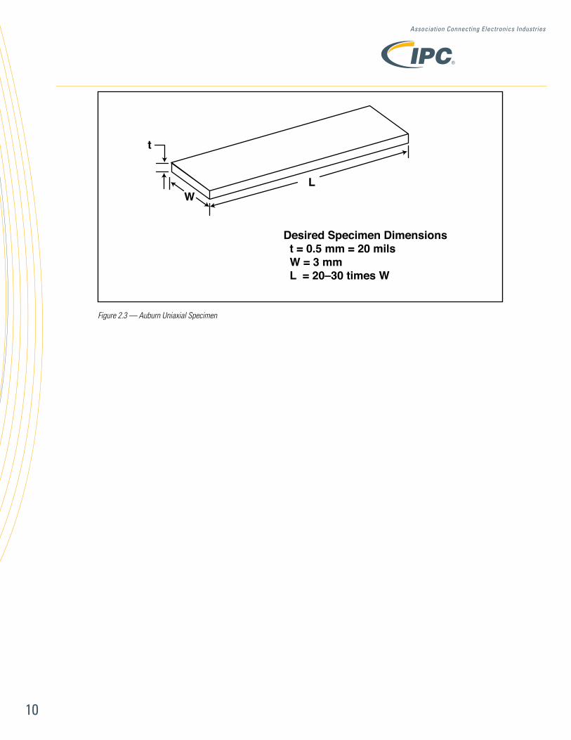
An advanced specimen preparation process has been developed using rectangular cross-section, small glass tubes [Wilmad/Labglass, Part Number P-.5X3M-120M] and a controlled vacuum system (Figure 2.2). The solder is melted in a quartz crucible (L=120mm, f=19mm) with a heating coil. A thermocouple and temperature control module are used to monitor and control the melting process temperature. After the temperature of the molten solder has maintained the desired temperature for 5 minutes, the rectangular cross-section glass tube connected to the controlled vacuum system is inserted into the molten solder and the molten solder is pulled into the glass tube. The glass tube is then immersed
in oil or cold water immediately after filling. Once the sample is cooled to room temperature, the specimen can be extracted due to the lower coefficient of thermal expansion of the glass compared to the solder (Figure 2.2). Figure 2.3 shows the dimensions of a specimen made by this process. Compared with the dog-bone or casting specimens used by other researchers, the thickness of the Auburn uniaxial specimen is close to that of real CSP (0.25~0.5mm) and BGA (0.5mm) solder joints. This new specimen replicates the solder joint thermal history of typical electronic packages and also separates the specimen from the effects of other variables.
APPENDIX A: SAMPLE PREPARATION (CourtesyofR.WayneJohnsonandQingWang,AuburnUniversity)
(a) Solder Melting System
(b) Specimen solidified in glass tube (c) Specimen after removal from glass tube
Figure 2.2 — Solder Melting System and Specimen Preparation
®
Association Connecting Electronics Industries
10
Figure 2.3 — Auburn Uniaxial Specimen
t
L
Desired Specimen Dimensions t = 0.5 mm = 20 mils W = 3 mm L = 20–30 times W
W