andreas ess, tobias gysi signal processing tasks for rhwosas main part of this thesis, an...
TRANSCRIPT
Eidgenössische Technische Hochschule ZürichSwiss Federal Institute of Technology Zurich
Andreas Ess, Tobias Gysi
Signal Processing Tasks for RHWOS
Student Thesis SA-2004-11Winter Term 2003/2004
Tutors:Herbert Walder andMatthias Frey
Supervisors:Prof. Dr. H.-A. Loeliger andProf. Dr. L.Thiele
6.2.2004
Institut für Technische Informatik und KommunikationsnetzeComputer Engineering and Networks Laboratory

Abstract
In this semester thesis, we present both a VGA driver, as well as two signal processingtasks (turbo decoder, spectrum analyzer) for the [9]. As these two topicsare mostly independent, the paper is split into two parts.
First, an overview of the VGA driver is given, including a sample applicationdemonstrating how to use it for other tasks’ purposes. This is mainly thought of asa reference for the user of the driver, but also contains enough information on the in-ternals for further development.
Then, as sample tasks for the ’s Reconfigurable Hardware OperatingSystem (RHWOS), two computationally intensive signal processing applications werechosen.First, a spectrum analyzer task is discussed. We focus on the basic building blocks, andthe few steps that yet have to be taken to actually put it to work.As main part of this thesis, an implementation of a turbo decoder according to theUMTS specifications is presented. In the respective chapter, we deal with an overviewover the algorithm, considerations when translating it to hardware, and qualitative com-parisons between ASIC and FPGA implementations.
III


Acknowledgements
It was very instructional to be able to work on such an interdisciplinary semester thesis.This would not have been possible without the help of a lot of people, who we wouldlike to acknowledge in this section.
We would like to thank our advisors Herbert Walder and Matthias Frey. Both haveprovided valuable information throughout the whole project. They invested much oftheir time, and many of their advices helped to make this project what it is.We also very much appreciate the help of Prof. Loeliger, who came up with the sug-gestion of implementing a turbo decoder, and thus allowed us to actually tackle thisinterdisciplinary project. He took the time on several occasions to explain things to usand gave useful input to this project.Thanks to Prof. Thiele for his confidence in this project and providing the infrastruc-ture at TIK.Thanks go to Christian Plessl as well, who has provided us with some useful informa-tion concerning differences between FPGAs and ASICs.Last but not least, we would also like to thank the other students working in the sameroom. They have provided a pleasant and helpful atmosphere, and it was not onlyinstructional, but also fun to work with them in a team.
V

VI
Contents
1 Introduction 11.1 Reconfigurable Hardware Operating System. . . . . . . . . . . . . . 11.2 XFBoard platform. . . . . . . . . . . . . . . . . . . . . . . . . . . . 1
2 VGA Driver 32.1 Introduction. . . . . . . . . . . . . . . . . . . . . . . . . . . . . . . 32.2 Features. . . . . . . . . . . . . . . . . . . . . . . . . . . . . . . . . 32.3 Requirements. . . . . . . . . . . . . . . . . . . . . . . . . . . . . . 32.4 Overview . . . . . . . . . . . . . . . . . . . . . . . . . . . . . . . . 42.5 VGA core . . . . . . . . . . . . . . . . . . . . . . . . . . . . . . . . 42.6 VGA driver . . . . . . . . . . . . . . . . . . . . . . . . . . . . . . . 5
2.6.1 Line buffer . . . . . . . . . . . . . . . . . . . . . . . . . . . 62.7 Window manager. . . . . . . . . . . . . . . . . . . . . . . . . . . . 62.8 Memory manager. . . . . . . . . . . . . . . . . . . . . . . . . . . . 7
2.8.1 Timing diagram. . . . . . . . . . . . . . . . . . . . . . . . . 82.9 Internals. . . . . . . . . . . . . . . . . . . . . . . . . . . . . . . . . 9
2.9.1 VGA driver internals. . . . . . . . . . . . . . . . . . . . . . 92.9.2 Window manager internals. . . . . . . . . . . . . . . . . . . 92.9.3 Memory manager internals. . . . . . . . . . . . . . . . . . . 102.9.4 Timing . . . . . . . . . . . . . . . . . . . . . . . . . . . . . 11
2.10 Demo application. . . . . . . . . . . . . . . . . . . . . . . . . . . . 122.10.1 Compiling the demo application. . . . . . . . . . . . . . . . 13
2.11 Notes . . . . . . . . . . . . . . . . . . . . . . . . . . . . . . . . . . 132.11.1 Microblaze . . . . . . . . . . . . . . . . . . . . . . . . . . . 132.11.2 Font routines. . . . . . . . . . . . . . . . . . . . . . . . . . 13
3 Spectrum Analyzer 153.1 Introduction. . . . . . . . . . . . . . . . . . . . . . . . . . . . . . . 153.2 Features. . . . . . . . . . . . . . . . . . . . . . . . . . . . . . . . . 153.3 Overview . . . . . . . . . . . . . . . . . . . . . . . . . . . . . . . . 153.4 FFT core. . . . . . . . . . . . . . . . . . . . . . . . . . . . . . . . . 153.5 Root core . . . . . . . . . . . . . . . . . . . . . . . . . . . . . . . . 16
3.5.1 Extracting root in Hardware. . . . . . . . . . . . . . . . . . 173.6 Putting it all together. . . . . . . . . . . . . . . . . . . . . . . . . . 173.7 Limitations . . . . . . . . . . . . . . . . . . . . . . . . . . . . . . . 183.8 Further steps. . . . . . . . . . . . . . . . . . . . . . . . . . . . . . . 19
VII

VIII CONTENTS
4 Turbo Decoder 214.1 Turbo codes - overview. . . . . . . . . . . . . . . . . . . . . . . . . 21
4.1.1 Turbo encoder. . . . . . . . . . . . . . . . . . . . . . . . . 214.1.2 Channel. . . . . . . . . . . . . . . . . . . . . . . . . . . . . 224.1.3 Turbo decoder. . . . . . . . . . . . . . . . . . . . . . . . . 22
4.2 Implementation. . . . . . . . . . . . . . . . . . . . . . . . . . . . . 244.2.1 Code in use. . . . . . . . . . . . . . . . . . . . . . . . . . . 244.2.2 Forward-backward algorithm. . . . . . . . . . . . . . . . . . 244.2.3 Interleaver . . . . . . . . . . . . . . . . . . . . . . . . . . . 284.2.4 Memory considerations. . . . . . . . . . . . . . . . . . . . . 304.2.5 Putting it all together. . . . . . . . . . . . . . . . . . . . . . 31
4.3 Testing environment. . . . . . . . . . . . . . . . . . . . . . . . . . . 324.3.1 PC application (encoder). . . . . . . . . . . . . . . . . . . . 324.3.2 XFBoard (decoder). . . . . . . . . . . . . . . . . . . . . . . 33
4.4 Results. . . . . . . . . . . . . . . . . . . . . . . . . . . . . . . . . . 344.4.1 Performance - bit errors. . . . . . . . . . . . . . . . . . . . 344.4.2 Performance - execution time. . . . . . . . . . . . . . . . . 354.4.3 ASIC . . . . . . . . . . . . . . . . . . . . . . . . . . . . . . 36
4.5 Further steps. . . . . . . . . . . . . . . . . . . . . . . . . . . . . . . 374.6 Running the demo. . . . . . . . . . . . . . . . . . . . . . . . . . . . 40
4.6.1 Software needed. . . . . . . . . . . . . . . . . . . . . . . . 404.6.2 Compiling the demo. . . . . . . . . . . . . . . . . . . . . . 404.6.3 Running the demo. . . . . . . . . . . . . . . . . . . . . . . 41
5 Conclusion 43
6 CD 45
Chapter 1
Introduction
1.1 Reconfigurable Hardware Operating System
Reconfigurable systems in general have a great potential to not only speed up applica-tions, but also save chip area. On top of that, the system can be made more flexible.To give a quick example, there exist many versions of turbo decoders. A native ASICimplementation needs support for each standard built in, whereas a reconfigurable ver-sion can easily specialize on one decoder type. A different version can then be easilyobtained by reconfiguring the FPGA.
Thus, a good system would run on a reasonably small FPGA, and dynamicallyload tasks on demand from some sort of external memory. This asks for some sort ofhardware operating system that manages the scheduling of resources.
1.2 XFBoard platform
This semester thesis was done in the scope of the X-Forces project, which is supposedto show the possibilities and limits of such a reconfigurable hardware operating system.
In [9], a demonstration board was developed specifically for this project. Figure1-1 shows an abstract overview over the board. The core is formed by two FPGAs. Ontop, there’s the C-FPGA (CPU), which handles resources and tasks for the R-FPGA(reconfigurable). A possible application now can run large parts of the code on theC-FPGA, and swap out data-flow intensive parts directly to hardware in order to dra-matically speed up calculations.
This thesis concentrates on the R-FPGA part of the system. It was necessary todevelop a means for the tasks to output their information on the screen, thus the VGAdriver.The RHWOS is currently being developed in [10] and [12]. As it is not completelyready yet, the spectrum analyzer and turbo decoder tasks are currently running entirelyon the R-FPGA.
1

2 CHAPTER 1. INTRODUCTION
Virtex-IIC-FPGA
Virtex-IIR-FPGA
SDRAM Left16M X 16
SDRAM Right16M X 16
SRAM Left1M X 32
SRAM Right1M X 32
SDRAM16M X 32
SRAM1M X 32
FlashRAM4M X 32 BootPROM
EthernetPHY
EthernetPHY
AudioCoDec
VideoDAC
8-LED Bar
2 LEDs2 Switches
2 LEDs2 Switches
JTAG6 Pin Header
JTAG6 Pin Header
VGA Out15 Pin D-SUB HD
VGA Out15 Pin D-SUB HD
EthernetRJ-45
Eth
erne
tR
J-45
PS/2
6 Pi
n M
iniD
IN
PS/2
6 Pi
n M
iniD
IN
RS-232
9 Pin D-SU
B
RS-2329 Pin D-SUB
RS-2329 Pin D-SUB
Aud
io I
n 1
3.5m
m m
ono
Jack
Aud
io I
n 0
3.5m
m m
ono
Jack
Audio Out3.5mm mono Jack
Expansion Slot36 Pin Header
Expansion Slot40 Pin Header
Data SignalsConfiguration Signals
Figure 1-1: XFBoard - Scheme

Chapter 2
VGA Driver
2.1 Introduction
As part of the RHWOS project [14], the first task was to design an appropriate VGAdriver for the R-FPGA part of the system.A hardware based multi-window approach was chosen. The main reason for this was totake the burden of implementing a windowing system from the RHWOS. Furthermore,this facilitates the handling of windows for the tasks themselves. A task can access itspart of the screen without worrying about the window position or other tasks.
The VGA driver was also used later in the course of our project to display the outputof the turbo decoder sample application.
2.2 Features
• 640 · 480 px standard VGA resolution at a refresh rate of60 Hz
– adjustable by recompilation
• 16 bit color depth
• up to4 independent windows
– separate video RAM area for each task
– freely moveable and sizeable
– double-buffering capability
• memory independent test picture
2.3 Requirements
• Assumes 50 MHz clock for monitor timing
• 1 BlockRAM for temporary line buffer
• 405 out of14′336 slices (2%)
3

4 CHAPTER 2. VGA DRIVER
• 323 out of28′672 slice flip flops (1%)
• 710 out of28′672 input LUTs (2%)
• 1 DCM (optional, for different resolutions)
2.4 Overview
As seen in picture2-1, the VGA core is partitioned into three parts:
• the VGA driver is the actual interface to the DAC
• the window manager translates screen coordinates into the respective window’smemory addresses
• the memory manager handles concurrent accesses to the video memory
Application
Monitor SRAM
VGADriver Window Manager Memory Manager
vgacore.vhdvgadriver.vhd winmgr.vhd memmgr.vhd
Figure 2-1: VGA core - scheme
These three parts are linked together in a top file (vgacore.vhd ) that providesthe most important signals to the user. None of the input data is registered, that meanswindow positions, etc. have to be kept as long as they are valid. Changes in positionand size are applied immediately, which can result in an unstable picture for one frame.
The next sections describe the parts and their respective interfaces in detail.
2.5 VGA core
The VGA core, found invgacore.vhd , is the interface to the tasks and handles theinternal connections between the three units stated above. Signals provided to the userare described below in the pertaining sections.
2.6. VGA DRIVER 5
The VGA core needs one of Virtex2’s BlockRAMs for local buffering. This isneeded to burst lines from RAM into a local buffer, from where the actual drawingtakes place.
Note: Using a DCM, these bursts could be made faster, such that less time is usedby the VGA driver to access memory.A DCM requires a buffered clock input using IBUFG. This, however, means that noother part of the design can directly access the original clock pad—instead, everythingmust work on the buffered clock that is also fed to the VGA core. It’s thus needed toinstantiate an IBUFG at the top level and provide the rest of the design with its output.
Signal Meaning
CLKxCI 50 MHz clock signalRSTxRI Reset signal
Table 2-1: General signals
2.6 VGA driver
The VGA driver,vgadriver.vhd , has two concurrent processes: the first one buffersan entire line from memory into a FIFO at a clock period of20 ns, the second one doesthe actual VGA drawing at25 MHz from this buffer.
Monitor timing is done according to [13]. A pixel clock of 25 MHz yields a screenrefresh rate of60 Hz at640 · 480 px. Higher resolutions or rates are possible. How-ever, these would not only reduce the available memory bandwidth for applications butwould also require an additional DCM to accommodate to the necessary pixel clock.Still, this is possible by adjusting the constants at the beginning of the file, in additionto clocking the processVGACLKxCI_P with an appropriate DCM.
To implement the FIFO buffer, one of the Virtex2’s own BlockRAMs is used. Abuffer size of512 pixels (16 bit, thus1′024 bytes) is used. While this can’t hold anentire line, drawing is started early enough to prevent buffer overflow.
Signal Meaning
RxD Red signal (8 bit)GxD Green signal (8 bit)BxD Blue signal (8 bit)PCLK Pixel clock for RAMDACHSYNCB Horizontal syncVSYNCB Vertical sync
Table 2-2: Output signals to video DAC
6 CHAPTER 2. VGA DRIVER
Signal Meaning
VGABlack Set high for black screenVGATest Set high for test picture
Table 2-3: VGA driver, input signals
2.6.1 Line buffer
The FIFO used for buffering lines was generated from an asynchronous FIFO usingXilinx’s CoreGen [19]. The file linebuffer.xco holds all necessary information.In order to compile it, one has to select the option “Regenerate core” in the XilinxProject Navigator. Also, “View VHDL Function Model” might be necessary to get itworking.
Please refer to section2.10on page12 for detailed information on how to compilea test project with the VGA driver.
2.7 Window manager
The window manager,winmgr.vhd , receives screen coordinates from the VGA driverand then translates these to the appropriate memory addresses. A standard backgroundcolor is used for pixels not covered by windows.
For each window (W1x . . .W4x), the input signals stated in table2-4are provided.These are not registered and must thus be kept active throughout their life cycle.
Signal Meaning
W1xX X coordinate of window(0 . . . 639)W1xY Y coordinate of window(0 . . . 479)W1xW Width of window(0 . . . 639)W1xH Height of window(0 . . . 479)W1xMemPage1 Base address of first buffer (20 bit)W1xMemPage2 Base address of second buffer (20 bit)W1xBID Buffer to display (0 = first buffer)W1xValid Set high to show window
Table 2-4: Per-window signals
Two buffers can be defined by the user, with the signalW1xBID selecting whicharea to draw from. This can be used to implement double buffering: while one bufferis displayed, the other is updated with new information. As soon as this data is ready,the buffers are exchanged by flipping theW1xBID signal.
Besides the signals defined for all windows, there’s two global signals, as seen intable2-5.

2.8. MEMORY MANAGER 7
First, the background color will fill the entire space not covered by windows. For test-ing purposes, a switch has been implemented which bypasses the memory managerand uses a single fill color for all windows instead.
Signal Meaning
WxBG Background color (16 bit RGB)WxTest Replaces contents of windows by a single color
Table 2-5: General signals
The background color is given as a16 bit value, given in5 − 6 − 5 representation,as seen in table2-6.
R R R R R G G G G G G B B B B B15 0
Table 2-6: RGB representation in a 16 bit word
2.8 Memory manager
The memory manager,memmgr.vhd , provides the actual interface to write image datainto. The SRAM [1] on the left side of the R-FPGA is used as video memory.
Since the SRAM is not dual-port, a simple access management was implemented.General rule is that the window manager has highest priority and can suspend any otheraccesses to the memory. This ultimately means that at any given point in time, a taskmight have to wait for a period of a whole line to be fetched into the VGA driver’sbuffer.
This, and the possibility to have the VGA core itself run at a higher clock rate, ledto the implementation of an asynchronous protocol for accessing the SRAM. As a sideeffect, the task doesn’t have to worry about access timing for SRAM.In section2.8.1, read and write waveforms for accessing the memory manager aregiven.
Table2-7gives per-window signals for reading and writing data from/to the SRAM.
Note: read data is registered - i.e. as soon asW1xACKis set, the memory managercan continue serving other requests, while the data inW1xDataOut will stay valid.
Finally, the memory manager’s output pins have to be connected to the left SRAMbank of the using the signals from table2-8.

8 CHAPTER 2. VGA DRIVER
Signal Meaning
W1xAddr Address of memory (20 bit)W1xDataIn Data to be written (16 bit RGB)W1xDataOut Read data (registered) (16 bit RGB)W1xREn Read enableW1xWEn Write enableW1xACK Asynchronous ack
Table 2-7: Per-window signals for memory manager
Signal Meaning
Addr Address in SRAMData DataA19B Inverted MSb of addressWEn Write enable
Table 2-8: Connections to SRAM
2.8.1 Timing diagram
Example write waveform
Figure 2-2: Write wave form
The write wave form seen in2-2 was generated by the behavioural simulation ofthe demo program given in section2.10.To write, address and data have to be valid at the timeW1xWEnis set to1. Writing isfinished as soon asW1xACK is set to1. To actually finish the write process,W1xWEnhas to be taken down again. This cancelsW1xACK and makes the memory managerready for new data.
The reading process is analogous to writing.

2.9. INTERNALS 9
2.9 Internals
2.9.1 VGA driver internals
The VGA driver continously feeds the DAC with the necessary information to draw thescreen. It can be switched off withVGABlack . The signalVGATest draws a testpicture.By default, the picture is read from memory, buffered locally and then drawn to thescreen.
The interface of the VGA driver can be splitted into three parts: control interface,connections to the window manager and outputs to the video DAC. The window man-ager is controlled by the two signalsPixelX andPixelY . Corresponding pixels arereturned with a delay of4 cycles. Then, the pixel value can be read fromPixelData .
The screen resolution is determined by the constants invgadriver.vhd . Tim-ing data for several resolutions can be found in [13].
Table2-9describes the different clocks and their use.
Clock Use
RAMCLKxCI Used for communication with the memory man-ager
VGACLKxCI 50 MHz main clock of the driverOurClk 25 MHz used for VGA output side, equivalent to
the pixel clockPCLK
Table 2-9: VGA driver clocks
The following processes are found in the VGA driver:
• ReadReg and ReadMemless fill the line buffer if necessary. The delay of thememory manager has to be taken into account. This is done using the counterFIFOWaiting .
• The pairVGACLKxCI andOurClk are responsible for generatingOurClkfor HSYNC, HCount and also for the read operation from the linebuffer.
• VCounter increments VCount after each horizontal synchronization signal
• VSyncB produces the vertical synchronization signal.
• Blitter is the main process. It either writes theFIFOOut to the output or gener-ates the test picture.
2.9.2 Window manager internals
The window manager handles the translation of screen coordinates to memory ad-dresses.
10 CHAPTER 2. VGA DRIVER
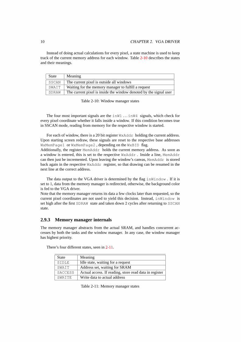
Instead of doing actual calculations for every pixel, a state machine is used to keeptrack of the current memory address for each window. Table2-10describes the statesand their meanings.
State Meaning
SSCAN The current pixel is outside all windowsSWAIT Waiting for the memory manager to fulfill a requestSDRAW The current pixel is inside the window denoted by the signal user
Table 2-10: Window manager states
The four most important signals are theinW1 . . .inW4 signals, which check forevery pixel coordinate whether it falls inside a window. If this condition becomes truein SSCAN mode, reading from memory for the respective window is started.
For each of window, there is a 20 bit registerWxAddr holding the current address.Upon starting screen redraw, these signals are reset to the respective base addressesWxMemPage1or WxMemPage2, depending on theWxBID flag.Additionally, the registerMemAddr holds the current memory address. As soon asa window is entered, this is set to the respectiveWxAddr . Inside a line,MemAddrcan then just be incremented. Upon leaving the window’s canvas,MemAddr is storedback again in the respectiveWxAddr register, so that drawing can be resumed in thenext line at the correct address.
The data output to the VGA driver is determined by the flaginWindow . If it isset to1, data from the memory manager is redirected, otherwise, the background coloris fed to the VGA driver.Note that the memory manager returns its data a few clocks later than requested, so thecurrent pixel coordinates are not used to yield this decision. Instead,inWindow isset high after the firstSDRAWstate and taken down2 cycles after returning toSSCANstate.
2.9.3 Memory manager internals
The memory manager abstracts from the actual SRAM, and handles concurrent ac-cesses by both the tasks and the window manager. In any case, the window managerhas highest priority.
There’s four different states, seen in2-11.
State MeaningSIDLE Idle state, waiting for a requestSWAIT Address set, waiting for SRAMSACCESS Actual access. If reading, store read data in registerSWRITE Write data to actual address
Table 2-11: Memory manager states

2.9. INTERNALS 11
Accesses to the SRAM by the tasks are handled in form of a simple Request-Acknowledge protocol. This is because in every state, when the window managerissues an request, other accesses have to be suspended in order to ensure a stable pic-ture. This means that in the worst case, a task has to wait for an entire line to be burstedfrom SRAM before its own request can be fulfilled.
The signaluser indicates the current user of the SRAM. Depending on this, theregisterRAddr holds the address currently fed to the SRAM.
Timing of reading and writing is done according to [1], assuming a50 MHz clock.
2.9.4 Timing
Since both window manager and memory manager are states machines waiting for arequest from outside, timing is slightly tricky. It takes a few clocks for a pixel requestfrom the VGA driver to be served. But as a pixel has to be served every two cycles (as-suming the ’s standard50 MHz clock), this process has to be pipelined.The resulting timing diagram can be seen in figure2-3.
1
2
5
43
6
Figure 2-3: VGA internal timing - overview
Here is a rundown of what is happening in the above wave form:
1. When drawing of a line is started,FIFOWaiting is decremented.
2. One cycle afterFIFOWaiting reaches0, the writing to the buffer is started.
3. Meanwhile,PixelX is incremented, and upon reaching the 4th pixel (in thisexample), theinW1 flag is set.
4. The window manager changes from scanning into drawing state, passing on re-quests to the memory manager.
5. The memory manager delivers the data read withSACCESS.
6. Data is written on rising clock edge into the FIFO.

12 CHAPTER 2. VGA DRIVER
2.10 Demo application
In order to demonstrate the usage of the VGA core, we compiled a small demo applica-tion that writes a pattern into video memory, and displays a test picture upon pressingthe ’s switch.
The following code framgment shows the part that is used to write the pattern tovideo memory using the memory manager.
-- This example state machine writes stripes into the video memory-- WAddr ... address to write to-- WData ... data to be written-- W1xWEn ... write enable signal-- State ... current statereg : process (CLKIN_IBUFG, RSTxRI)begin
if RSTxRI = ’1’ thenState <= SADDR;WAddr <= ( others => ’1’);
elsif CLKIN_IBUFG’event and CLKIN_IBUFG = ’1’ thenState <= nextState;WAddr <= nextWAddr;
end if ;end process ;
memless : process (State, WAddr, W1xACK)begin
nextWAddr <= WAddr;nextState <= State;W1xWEn <= ’0’;
-- Combinatorial calculation of data based on addressif WAddr(0) = ’0’ then
WData <= ( others => ’0’);else
WData(3 downto 0) <= WAddr(3 downto 0);WData(14 downto 4) <= ( others => ’0’);
end if ;WData(15) <= WAddr(19);
case State iswhen SADDR =>
-- 1st step: if ACK is down again, mem manager-- is ready to receive new data: set write enableif W1xACK = ’0’ then
W1xWEn <= ’1’;nextState <= SWAIT;
end if ;
when SWAIT =>-- 2nd step: wait for ACKW1xWEn <= ’1’;
if W1xACK = ’1’ then-- ACK received, take down request-- increment addressnextState <= SADDR;nextWAddr <= WAddr + 1;W1xWEn <= ’0’;
end if ;
when others =>nextState <= SWAIT;
end case ;end process ;
2.11. NOTES 13
2.10.1 Compiling the demo application
The demo application described above can be found on the accompanying CD, seechapter6 on page45.
Open the corresponding filevgademo.vhd in the Xilinx Project Navigator, andselect “Generate programming file”.
2.11 Notes
For simplicity’s sake, this implementation of the VGA core uses a lot of signals, in-stead of providing an interface that would allow the user to pick a window and then usesome control information to set the required datum.
Furthermore, the possibility is provided to clock the memory accesses at a higherspeed, thus increasing the possible throughput. This was removed because of timingproblems.
On the feature side, overlapping windows are not supported yet. This change shouldnot be too difficult, but was left off due to the fact that it is not that important.
2.11.1 Microblaze
In [15], a few routines were developed for the Microblaze soft processor that allowaccess to the VGA driver’s most important signals. These routines were used in boththe spectrum analyzer and turbo decoder task for displaying their respective output.
2.11.2 Font routines
The following routines can be used to write out text or numbers inside a window. A6·8font is provided, but other fonts can be defined. All of these routines take advantage ofthe pixel writing routines developed in [15].
The common parameters to all these functions are the base pointer of the window,the color of the font, as well as the x, y position to plot the character(s) at. In order tocorrectly calculate the address inside the window, the width has to be specified as well.
void f_putc(Xuint32 baseptr, Xuint16 color, Xuint16 x,Xuint16 y, Xuint16 wdt, char c);
Prints a single character.
Xuint16 f_puts(Xuint32 baseptr, Xuint16 color, Xuint16 x,Xuint16 y, Xuint16 wdt, char * s);
Prints out an entire string and returns the x position directly following the strings.
Xuint16 f_putnum(Xuint32 baseptr, Xuint16 color, Xuint16 x,Xuint16 y, Xuint16 wdt, Xuint32 num, Xuint8 base);
Prints out the numbernum in the correspondingbase . Returns x position directlyfollowing the printed number.
void f_printf(Xuint32 baseptr, Xuint16 color, Xuint16 x,Xuint16 y, Xuint16 wdt, const char * ctrl1, ...);

14 CHAPTER 2. VGA DRIVER
Writes out a formatted string, with the same basic arguments inside the formatstrings as the ANSI C function printf.

Chapter 3
Spectrum Analyzer
3.1 Introduction
As a first signal processing task for the RHWOS, a spectrum analyzer was imple-mented. It reads an audio signal from the audio driver and displays the correspondingspectrum on the screen. In the following sections, the general layout of this task isdescribed.
3.2 Features
• 44.1 kHz, mono audio input
• 16 bit resolution
• 1′024 point FFT
• Output using VGA driver (32 bars displayed on-screen)
3.3 Overview
The spectrum analyzer is partitioned into3 hardware parts and control software runningon an instance of the Microblaze soft processor.
• wrapper for the audio driver
• FFT core
• root core
• Microblaze with control software and graphics output
3.4 FFT core
To perform the Fourier transfomation, a Xilinx core is used. Therefore, it was onlynecessary to study the interface and develop a suitable wrapper. The wrapper, seen infigure3-1, reads data from an input FIFO, calculates the FFT and writes the result to an
15

16 CHAPTER 3. SPECTRUM ANALYZER
output FIFO. Both FIFOs have to provide enough space for1′024 values. As the FFTcalculates a complex number with imaginary and real parts of16 bits each, the outputhas to be32 bits wide.
Configure FFT
Xilinx FFT Corefifoin buffifo
fftwrapper.vhd
Figure 3-1: FFT wrapper
Table3-1describes the signals to control the wrapper.
Signal Meaning
go Start calculation. A full input FIFO expected.finished Set if data in output FIFO is ready.busy Set while core is calculating.idle Set when core is idle.rerror Core could not read enough data. Triggergo to
return to idle state.werror Write error occured. Triggergo to return to idle
state.
Table 3-1: Control interface for FFT wrapper
The wrapper is found infftwrapper.vhd . There, it is possible to change coreoptions, e.g. the size of the FFT and scaling options. For more details, refer to theXilinx core documentation [20].
3.5 Root core
The output of the FFT core consists of1′024 complex values. As the spectrum of a realsignal is symmetric, only the first512 values need to be processed by the root core, asseen in figure3-2. It calculates the absolute value by squaring both imaginary und realpart, sum them up and subsequently extracting the root from this number. Last, tuplesof 32 values are taken and averaged together to form a total of32 output values. These

3.6. PUTTING IT ALL TOGETHER 17
are the values that actually will be displayed.
rootwrapper.vhd
muladd.vhd root.vhd
real2 + imag2
buffifo fifoout
sqrt average
Figure 3-2: Root wrapper
The interface given in3-2 is very similar to the one of the FFT core.
Signal Meaning
go Start calculation. A full input FIFO is expected.finished Set if data in output FIFO is ready.idle Set if core is idle.rerror Core could not read enough data. Triggergo to
return to idle state.werror Write error occured. Triggergo to return to idle
state.
Table 3-2: Control interface for root wrapper
The main challenge of this part was the extraction of roots. As there was no alreadyrunning core available, this was implemented by hand. The squaring of imaginary andreal part is done using two Virtex2 block multipliers. The number of values to beaveraged is adaptable by a constant. The depth of the output FIFO then has to bechanged accordingly.
3.5.1 Extracting root in Hardware
The root algorithm calculates one bit per cycle, starting from the MSb.At the beginning, the result is set to zero and the current bit to the MSb. Then, thealgorithm checks if the square of the current result with current bit set is smaller thanthe input. If this is the case, the new result value is the old one with set current bit. Thisprocess is now repeated, decrementing the current bit until it reaches the LSb. Theresult is the integer root of the input.
3.6 Putting it all together
The three components audio, FFT and root are put together in one top file. The singlecomponents are connected by FIFOs. Figure3-3gives an overview over the data flow.
The control interfaces are connected to the Microblaze core. Furthermore,top.vhdintroduces logic for the Microblaze to read from the output FIFO. The following codefragment shows the code for one transformation.
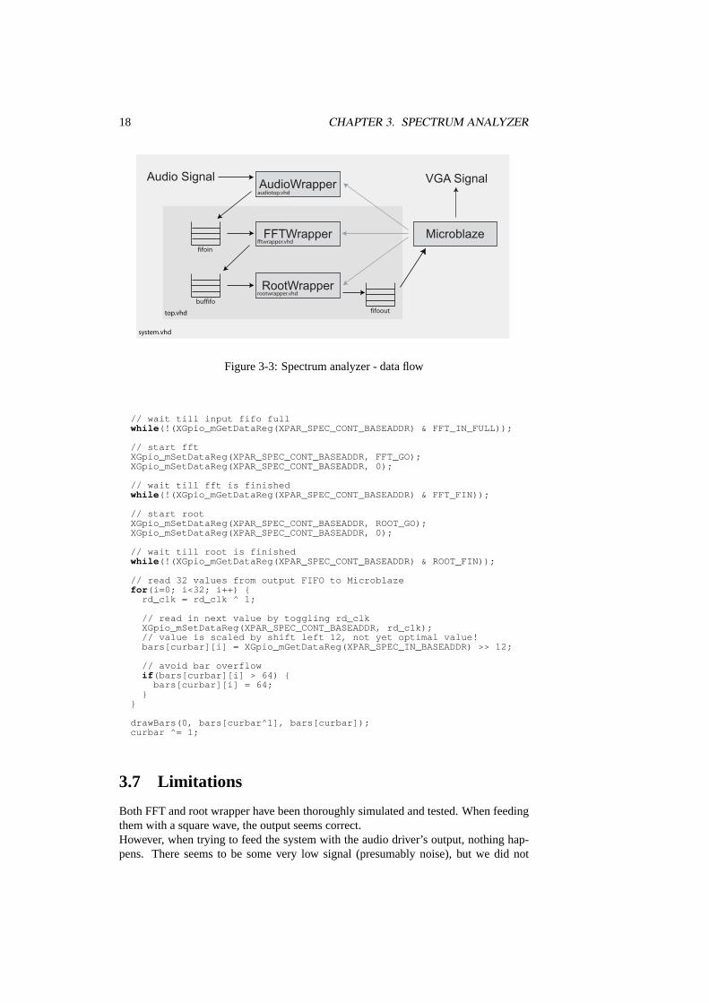
18 CHAPTER 3. SPECTRUM ANALYZER
system.vhd
top.vhd
AudioWrapper
FFTWrapper
RootWrapper
Microblaze
Audio Signal VGA Signal
fifoin
fifooutbuffifo
fftwrapper.vhd
audiotop.vhd
rootwrapper.vhd
Figure 3-3: Spectrum analyzer - data flow
// wait till input fifo fullwhile (!(XGpio_mGetDataReg(XPAR_SPEC_CONT_BASEADDR) & FFT_IN_FULL));
// start fftXGpio_mSetDataReg(XPAR_SPEC_CONT_BASEADDR, FFT_GO);XGpio_mSetDataReg(XPAR_SPEC_CONT_BASEADDR, 0);
// wait till fft is finishedwhile (!(XGpio_mGetDataReg(XPAR_SPEC_CONT_BASEADDR) & FFT_FIN));
// start rootXGpio_mSetDataReg(XPAR_SPEC_CONT_BASEADDR, ROOT_GO);XGpio_mSetDataReg(XPAR_SPEC_CONT_BASEADDR, 0);
// wait till root is finishedwhile (!(XGpio_mGetDataReg(XPAR_SPEC_CONT_BASEADDR) & ROOT_FIN));
// read 32 values from output FIFO to Microblazefor (i=0; i<32; i++) {
rd_clk = rd_clk ^ 1;
// read in next value by toggling rd_clkXGpio_mSetDataReg(XPAR_SPEC_CONT_BASEADDR, rd_clk);// value is scaled by shift left 12, not yet optimal value!bars[curbar][i] = XGpio_mGetDataReg(XPAR_SPEC_IN_BASEADDR) >> 12;
// avoid bar overflowif (bars[curbar][i] > 64) {
bars[curbar][i] = 64;}
}
drawBars(0, bars[curbar^1], bars[curbar]);curbar ^= 1;
3.7 Limitations
Both FFT and root wrapper have been thoroughly simulated and tested. When feedingthem with a square wave, the output seems correct.However, when trying to feed the system with the audio driver’s output, nothing hap-pens. There seems to be some very low signal (presumably noise), but we did not

3.8. FURTHER STEPS 19
manage to receive the actual signal fed to the audio input.
3.8 Further steps
To actually get this task working, the audio wrapper has to be revised. As soon as thisis working, only the software part should need some adaptation concerning the scalingof the bars.Other than that, we are confident that the system works.

20 CHAPTER 3. SPECTRUM ANALYZER
Chapter 4
Turbo Decoder
The Virtex2 FPGA chip [16] used on the XFBoard offers a very good basis for signalprocessing applications, since the V3000 version used for the R-FPGA has96 onboard18x18 bit multipliers. Using these multipliers in parallel, a great deal of concurrencycan be achieved, improving performance significantly in dataflow-oriented applica-tions.In our case, some parts of the system use up to18 multipliers in parallel, which resultedin almost the same performance as the corresponding PC application, even at the mod-est clock rate of50 MHz.
In the scope of this project, a turbo decoder according to the UMTS specificationswas implemented.
4.1 Turbo codes - overview
Turbo codes were introduced in 1993 by Berrou, Glavieux and Thitimajshima [3].The turbo codes considered in this project are based on 2 parallel concatenated con-volutional codes. The upper encoder is fed directly with the input sequence, while thesecond encoder receives an interleaved version of the same information sequence.
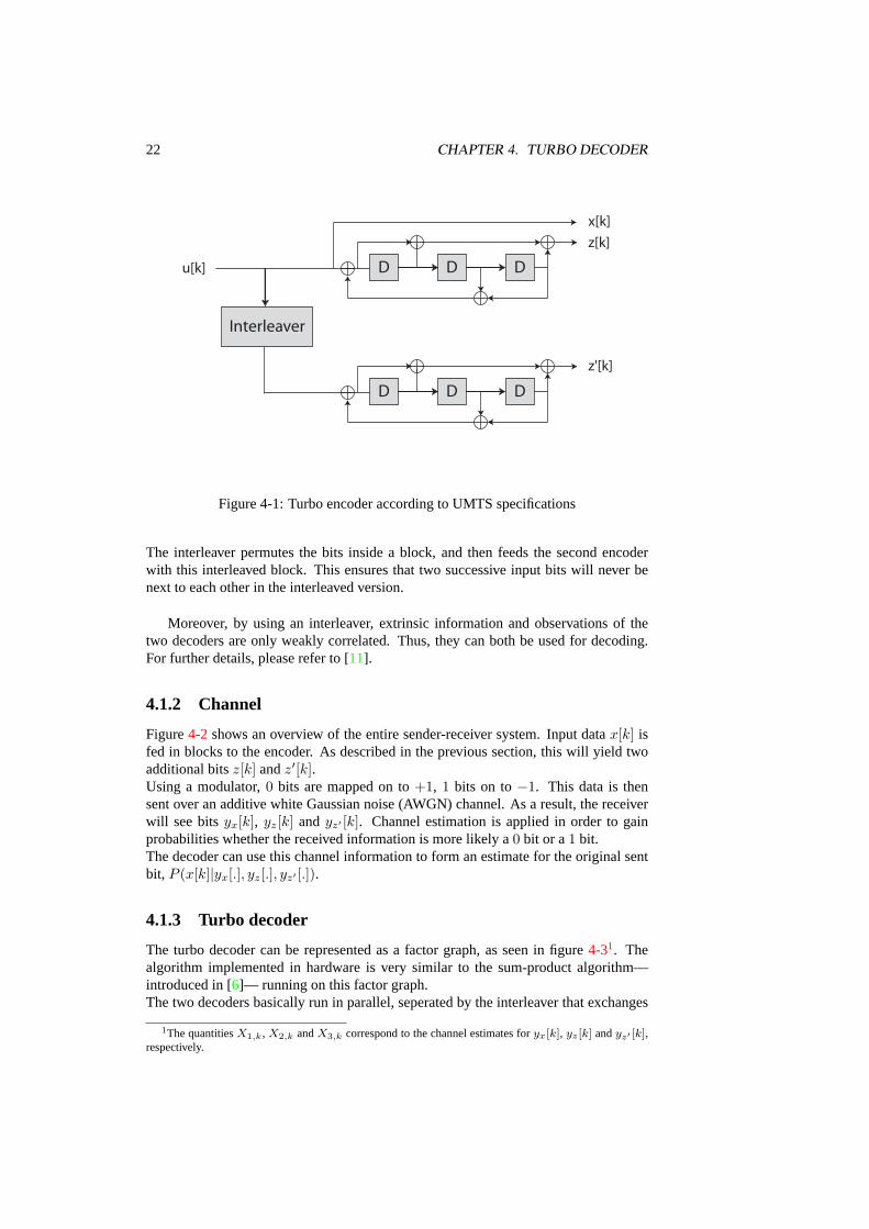
4.1.1 Turbo encoder
Figure4-1 shows the encoder suggested by the UMTS specifications. It adds redun-dancy to the input signal, such that the decoder can infer on the original signal despitenoise introduced by the channel.The basic idea is to split the input into blocks of lengthK, and transmit multiple bitsper single input bit over the channel. Whilex[k] is the same as the data input to theencoder,z[k] is formed by a convolutional encoder working directly on the input se-quence. Additionally, each block of the input is permuted by an interleaver, and thenfed to another convolutional encoder to formz′[k].
One of the main design issues for a linear code is to maximize the hamming weight.This is roughly the same as maximizing the weight of the minimum-weight codeword.On one hand, recursive codes are used for this, on the other, an interleaver.
21
22 CHAPTER 4. TURBO DECODER
x[k]
z[k]
z'[k]
u[k]
Figure 4-1: Turbo encoder according to UMTS specifications
The interleaver permutes the bits inside a block, and then feeds the second encoderwith this interleaved block. This ensures that two successive input bits will never benext to each other in the interleaved version.
Moreover, by using an interleaver, extrinsic information and observations of thetwo decoders are only weakly correlated. Thus, they can both be used for decoding.For further details, please refer to [11].
4.1.2 Channel
Figure4-2 shows an overview of the entire sender-receiver system. Input datax[k] isfed in blocks to the encoder. As described in the previous section, this will yield twoadditional bitsz[k] andz′[k].Using a modulator,0 bits are mapped on to+1, 1 bits on to−1. This data is thensent over an additive white Gaussian noise (AWGN) channel. As a result, the receiverwill see bitsyx[k], yz[k] andyz′ [k]. Channel estimation is applied in order to gainprobabilities whether the received information is more likely a0 bit or a1 bit.The decoder can use this channel information to form an estimate for the original sentbit, P (x[k]|yx[.], yz[.], yz′ [.]).
4.1.3 Turbo decoder
The turbo decoder can be represented as a factor graph, as seen in figure4-31. Thealgorithm implemented in hardware is very similar to the sum-product algorithm—introduced in [6]— running on this factor graph.The two decoders basically run in parallel, seperated by the interleaver that exchanges
1The quantitiesX1,k, X2,k andX3,k correspond to the channel estimates foryx[k], yz [k] andyz′ [k],respectively.

4.1. TURBO CODES - OVERVIEW 23
Encoderu[.]
x[.]
z[.]
P (yx[k]| x[k])
P (yz[k]| z[k])
P (yz′[k]| z[k])z′[.]
P(x
[k]|
yx[.],
yz[.],
yz
′[.])
Chan
nel
Est
imat
e
Turb
oD
ecoder
N (0, σ2)
Figure 4-2: Sender-receiver system with AWGN channel
the extrinsic information between the two. Equal gates are used to combine input in-formation (from the received data) with this extrinsic information.
Each box in the factor graph corresponds to a trellis section. Based upon the en-coder, the trellis can be constructed.
In order to maximize the a-posteriori probability of each information bit, the forward-backward algorithm is used inside each single decoder. Then, the newly gained infor-mation is exchanged with the other decoder.
After several iterations, a stable state is reached. A hard-decision is then made bycomparingP (x[k] = +1|yx[k], yz[k], yz′ [k]) againstP (x[k] = −1|yx[k], yz[k], yz′ [k]).
X1,k−1
=
X1,k
=
X1,k+1
=
· · ·
X2,k−1 X2,k X2,k+1
· · ·
“random” connections
· · ·
X3,k−1 X3,k X3,k+1
· · ·
Figure 4-3: Turbo decoder - Factor graph

24 CHAPTER 4. TURBO DECODER
4.2 Implementation
The implementation of the turbo decoder presented here was a three-step process.First, a software version, written in C, was written to evaluate the design later tobe translated to hardware. This mainly covered the analysis of sections with largeamounts of dataflow. These are prone to a hardware-based implementation. At thispoint, floating-point arithmetic was used.Next, the C code was adapted to use fixed-point arithmetic, as would be the case inhardware as well. This step was useful in order to analyze the behaviour of the algo-rithm with less arithmetic precision.In the final step, the most time-consuming parts—both interleaver and the forward-backward algorithm—were translated to hardware. Only the control flow between de-coding iterations was left to a C program running on the Microblaze [18] soft processor.
4.2.1 Code in use
The turbo code used for this project was constructed according to the UMTS specifi-cations [4]. A rate-1/3 code with a block length ofK = 4′900 was chosen. Besidesnicely fitting a 70x70 black and white picture for our testing environment, a higherblock length also provides better performance.
4.2.2 Forward-backward algorithm
While the factor graph seen in4-3 suggests a parallel execution of both decoders, aserial approach was chosen for several reasons:
• The software version inherently had to work in a serial fashion. The plan was toderive the hardware version directly from it.
• Even though enough arithmetic units were available in hardware, early analysisshowed that memory would be the main bottleneck. This is further explained insection4.5on page37.
• A single instance of the forward-backward algorithm almost fills an entire taskslot of the RHWOS. Thus, chip area (as restricted by the RHWOS) was notsufficient to run both decoders at the same time.
Linearized form
Instead of running the two decoders in parallel, the information flow was changed to:
• Run decoder 1 onyx[.] andyz[.]
• Interleave its extrinsic information, send it to decoder 2
• Run decoder 2 onyx′ [.] andyz′ [.]
• Deinterleave its extrinsic information, send it to decoder 1

4.2. IMPLEMENTATION 25
Decoder 1 Decoder 2Interleaver
Interleaver-1
P(yz[k]|z[k]) P(yx[k]|x[k]) P(yz'[k]|z'[k])P(yx'[k]|x'[k])
Figure 4-4: Internal flow of turbo decoder
Note that the received data only coversyx[.], yz[.] and yz′ [.]. The factor graphrepresentation elegantly provides decoder 2 with an interleaved version ofyx[.] on thefly. In this implementation,yx′ [.] was explicitly derived fromyx[.] before starting theactual iterations. This is depicted in4-4.
With the control flow between the two decoders resolved, the next step was toactually implement the decoder internals, i.e. the forward-backward algorithm.
Numerical considerations
Generally, literature suggests two approaches: the preferred implementation uses a log-likelihood approach, implicitly allowing for numbers of very different magnitude to berepresented in a smaller interval. This lends itself very well to a fixed-point, hardwarebased representation. This is discussed in [8].The difficulty of this approach is the log-likelihood arithmetic, which is not that intu-itive and easy to implement in hardware—approximations are suggested e.g. in [11].
Thus, an implementation using messages based on probabilities was chosen. Thissimplified the calculations inside the trellis a lot, as only standard multiplications andadditions were needed.However, there is an inherent loss of information when trying to represent real numbersas fixed-point numbers— preferably with few bits. Not only the integer representationof channel estimates, extrinsic information and internal signals proofs to be problem-atic.The state metricsµf (s) andµb(s) converge quickly to0 within a single iteration, andmake the decoder implementation very prone to numerical underflows. To resolve thisproblem, two measures were taken:
• Scaling. After each section of the trellis, state metrics were rescaled such thatfor each section, the maximum state metric would equal the maximum numberof the fixed-point representation. This scaling doesn’t affect the actual output of

26 CHAPTER 4. TURBO DECODER
the forward-backward algorithm, [6].
• Introduce a minimum number . Still with scaling, numbers with a magnitudeseveral times smaller than the current maximumµf (s) could wrongfully be as-sumed to be0. It is thus suggested to have a lower bound for the numbers. Whilethis introduces additional numerical errors to the calculation, it will prevent un-derflows. It is important to prevent these, as they would rendering the wholecalculation completely unuseable.
These measures were slightly simplified for the hardware version:After the actual calculation for a trellis section, scaling is done by bit-shifting the resultto the left until the most significant bit of one message is set.Instead of bounding all calculations by introducing extra comparators, logic was savedby simply fixing the lowest input bit of all multipliers to1.
Additionally, by setting the SNR of the channel estimation smaller than the onesuggested by the channel’s actual SNR, one basically “trusts” the calculation less. Thiscan compensate for numerical errors as well.
Data-flow analysis
The exact application of the forward-backward algorithm is described in [6]. Here, asmall example for calculating a single state metric is given. This is then used to pointout ways to introduce parallelism into the calculation.
Figure4-5shows a trellis section corresponding to one input-bitx[k]. State metricsfor a states are designated asµf (s), branch metrics for a branchb asµ(b).For a branchb, lst(b) and rst(b) define the left and right state, respectively.
Consider the states on the right side of figure4-5, i.e. statess ∈ S[k]. As an exam-ple, the new state metric for the states111 is calculated.
Branches are designated with two numbers: the first one representing the value ofthe original information bitx[k], the second forz[k]. Latter can be inferred from theencoder: depending on the state and information bitx[k], the decoder’s outputz[k] willdiffer. This is used to gain more confidence inside the trellis: not all combinations of1’s and0’s can be used.There are two branches leading tos111: the first one,b0, associated withyx[k] = +1andyz[k] = +1; the second one,b1, with yx[k] = −1 andyz[k] = −1.µf (s111) can now be calculated as follows:
µf (s111) = µf (lst(b0)) · µ(b0) + µf (lst(b1)) · µ(b1)
The branch metricsµ(b0) andµ(b1) combine the channel estimates foryx[k], yz[k]and the extrinsic information gained from the other decoder, here calledP (x[k] = +1)andP (x[k] = −1), respectively.
The extrinsic information, as well as the channel estimates foryx[k], are derivedfrom the same information bit. Thus, they are first combined by an equal gate, heredenoted as equ(+1) and equ(−1).

4.2. IMPLEMENTATION 27
Figure 4-5: Section of a trellis
equ(+1) =P (yx[k]|x[k] = +1)P (x[k] = +1)
P (yx[k]|x[k] = +1)P (x[k] = +1) + P (yx[k]|x[k] = −1)P (x[k] = −1)
equ(−1) =P (yx[k]|x[k] = −1)P (x[k] = −1)
P (yx[k]|x[k] = +1)P (x[k] = +1) + P (yx[k]|x[k] = −1)P (x[k] = −1)
Note that the denominator is only for scaling purposes—it is omitted in the hard-ware version.Furthermore, the result of the equal gate has to be computed only once for each sectionof the trellis.
Now, the branch metrics can be calculated as:
µ(b0) = P (yz[k]|z[k] = +1) · equ(+1)
µ(b1) = P (yz[k]|z[k] = −1) · equ(−1)
Seeing that there are8 states for eachS[k], the above already suggests an obviouspoint to introduce parallelism. Basically, for a givenS[k], all µf (s) with s ∈ S[k] canbe calculated in parallel.Since it is advisable to have only one multiplication per cycle, the calculation is donein three cycles, as seen in table4-1. A peak parallelism of18 multiplications at thesame time is reached.

28 CHAPTER 4. TURBO DECODER
SFCALC1 Calculate result of equal gate (2 multiplications).For each branchb, multiply the channel estimateof yz[k] with corresponding state metric lst(b) (16multiplications)
SFCALC2 Multiply previous temporary results with equalgate (16 multiplications)
SFCALC3 Infer µf (s) by adding together previous tempo-rary results
Table 4-1: States of calculation
For the multiplications, the Virtex2’s on-board 18x18 bit multipliers were used.As the actual data was only8 bit wide, advantage was taken of the higher precision inintermediate calculation steps. This means that after the first calculation step,16 bitnumbers were used, the final result being32 bit. Because of this, scaling only had tobe applied at the very end of a trellis section.
4.2.3 Interleaver
Original implementation
The software implementation of the interleaver works exactly as the algorithm de-scribed in the UMTS specifications [4]. This yields a permutation array of sizeK,where each entry contains the new position of the corresponding interleaved bit.
Less memory
Because of its memory usage, it is not feasible to implement this algorithm in hardware.Therefore, an adapted version, which calculates the offsets on the fly, was written. Thisis only possible due to the fact that the forward-backward algorithm only accesses thedata sequentially.
To reach sufficient speed and at the same time, minimize the use of resources, thecalculations performed per step were limited to simple additions. The rest of the cal-culations were kept in pre-calculated tables.The result is code that uses less than300 constants and20 variables. This is an im-provement of more than a factor of10, compared to the original memory usage. Themain idea of the modified algorithm is that on each row, a specific row increment mod-ulo (P − 1) has to be added.
C implementation
This section deals with the adapted version of the interleaver. For simplicity’s sake,the backward iteration is not discussed - it can be obtained by mirroring the followingprogram code.
The following defines a function which stores the interleaved version ofdatasrcin datadest .
void interleave( int *datasrc, int *datadest)

4.2. IMPLEMENTATION 29
First, some constants are defined.s is an array with the standard permutation forone row.
int s[P] = {0, 5, 35, 215, ... , 91, 49, 48, 42, 6, 41
};
Another array holds the increment for each row. This guarantees that each row ispermuted differently.
int row_inc[ROWS] = {1, 7, 11, 13, 17, 19, 23, 29, 31, 37, 41, 43, 47,53, 59, 61, 67, 71, 73, 79
};
Each row has its own offset which is added to the permutation value. Therefore, alloffset values between0 and4′899 are generated.
int row_offset[ROWS] = {4750, 2250, 3500, 1000, 0, 500, 1250, 1750, 3000, 4500,2500, 2000, 3250, 4250, 750, 250, 4000, 1500, 3750, 2750
};
Actual code:// current value for each rowint row[ROWS];
// variablesint j, i;int count;
// initfor (j=0; j<ROWS; j++)
row[j] = 0;count = 0;
// iterating through matrix
// for all columns calcualte next value in rowfor (i=0; i<COLS; i++) {
// for all rows calc valfor (j=0; j<ROWS; j++) {
if ((count < K) && (s[row[j]] + row_offset[j] < K)) {// if we’re not yet finished (count < K)// and the result is valid then permute
// s[row[j]] + row_offset[j]// is now the interleaved value of countdatadest[count] = datasrc[s[row[j]] + row_offset[j]];
// further value written inc countercount++;
}
// calculate row permutation for next columnrow[j] = row[j] + row_inc[j];
// perform modulo operationif (row[j] >= (P-1))
row[j] -= (P-1);}
}}
Hardware version
The hardware version is the adaptation of this improved C code to VHDL.

30 CHAPTER 4. TURBO DECODER
The interleaver allows to read and write the data in both forward and backward di-rection, in either sequential or interleaved order.
An operation in interleaved mode normally takes2 cycles, in special cases up to4.For further information, please refer to the accompanying CD, described in chapter6on page45.
Adaptation to different blocksizes
It is possible to adapt the interleaver to different block sizesK with just a few changesin the code. Respective constants forK, P , etc. can be found in [4]. To simplify theadaptation, a software to calculate the constant arrays introduced above was developed.This is described in section6 on page45.When changingK, it is also advisable to change the size of the BlockRAM used forthe extrinsic information. This has to be done using the Xilinx CoreGenerator.
4.2.4 Memory considerations
Memory wise, the offers three possibilities for a task to store its data in:
• BlockRAM. Found on the Virtex2 chip, this memory is fast, but very limited—atotal of1′728 Kbits is available on the chip. The RHWOS will offer a maximumof 576 Kbits, i.e.72 KB, to a task.
• SRAM. A total of 4 MB is available,2 MB on either left and right side of thechip. Former is used for the VGA core, latter is still free.
• SDRAM. A total of 64 MB is available, but wasn’t considered due to the morecomplicated access and refresh control.
Note that SRAM and SDRAM is abstracted from using a basic memory managerthat is later to be replaced by the actual RHWOS’ memory manager.
The data to be stored by the turbo decoder is
• Extrinsic information. 4900 · 2 · 8 bitsFor each original information, bothP (x[k] = +1) andP (x[k] = −1) has to bestored.
• Channel estimates.4903 · 4 · 2 · 8 bitsThis is used for storing the valuesP (yx[k]|x[k] = +1), P (yx[k]|x[k] = −1),and the corresponding estimates foryz[.], yz′ [.], yx′ [.].
• State metrics.4904 · 8 · 2 · 8 bitsUsed to storeµf (s), µb(s). For every section of the trellis, there’s8 states, andtwo seperate memory areas are used for the forward and backward iteration.
This amounts to total a memory usage of127′488 bytes. In section4.5on page37,a way to drastically reduce this figure is presented.
We opted for the extrinsic information to be stored in BlockRAM, which also sim-plified the interleaver. Other data is stored in SRAM, including space to store the ex-trinsic information for both decoders—this is of interest in the last iteration when the
4.2. IMPLEMENTATION 31
extrinsic information of both decoders has to be combined for a hard-decision. This iscurrently done in software.
4.2.5 Putting it all together
The forward-backward algorithm, described infb.vhd , as well as the interleaver,given ininterleaver.vhd , form the main part of the decoder system. From a hard-ware point of view, these are complemented by the memory manager (memmanager.vhd ),a basic memory interface (basicmem.vhd ), as well as a top file (top.vhd ) puttingeverything together.
Controlling the decoder
To control the turbo decoder, the top file provides the interface shown in4-2.
Signal Meaning
fb_interleaved Switches the forward-backward algorithm to in-terleaved mode, i.e. data used isyx′ [.] andyz′ [.],and the interleaved extrinsic information. Thus,this is basically switching between the two de-coders.
fb_start Start a forward-backward iterationfb_done Indicates the end of an iterationint_init Initialize extrinsic information within interleaver
to 0.5int_rst Reset interleaver to start at first information bit
againint_tomem Write extrinsic information to memory, storage lo-
cation depends onio_interleavedint_done Acknowledges interleaver operationsio_write Write flagio_interleaved Interleaved flag. When not set, data is read/written
in sequential, otherwise in interleaved orderio_dataclk Data clock, data is transmitted on falling and ris-
ing clock edgeio_priors Reads extrinsic information from memory, infor-
mation from both decoders is transmitted in one32 bit value
io_xz Write or read channel estimates foryx[k] andyz[k] to memory, signal depends onio_writeandio_interleaved flags
io_done Set if input/output operation is finishedinput 32 bit input bus, used for write operationsoutput 32 bit output bus, used for read operations
Table 4-2: Controlling signals

32 CHAPTER 4. TURBO DECODER
To transmit data between the Microblaze and the decoder, a 32 bit wide interfaceis used. As the Microblaze is the slower part, it generates the data clock. To maximizeperformance, data is sent at rising and falling clock edge.
Memory manager
The memory manager is used for accessing the channel estimatesP (yx[k]|x[k] = +1),. . . and the state metricsµf (s) andµb(s). It abstracts from the actual memory by re-quiring another entity that gives access to data according to an address and a requestline.
Since the forward-backward algorithm accesses the data sequentially (either in for-ward or backward direction), the control signals were limited to a reset, step and ac-knowledge signal. The memory manager will then translate these to memory addresses(basis addresses are defined as constants at the beginning of the architecture), redirectthe request to the basic memory interface, and pass on the acknowledge to the forward-backward algorithm as soon as the data is read or written.
Note that especially the basic memory interface is platform dependent, and whenporting the program to another system using the Virtex2 FPGA, this has to be changedaccordingly.
4.3 Testing environment
To test our implementation, we opted for an environment as seen in figure4-6. Thegeneral idea was to simulate a noisy channel on the PC by adding random Gaussiannoise to the encoded data and to send this noisy data over Ethernet to theto be decoded.
Noise
Sender Encoder Decoder Sink
PC XFBoard
Ethernet
Figure 4-6: Testing environment
Note that the signal never leaves the digital domain. This would not be the case inan actual scenario. The testing application adds digital noise and sends the noisy signalto the decoder. In an actual application, a quantizer of some form would receive theanalog information and then feed the decoder with digital input.
4.3.1 PC application (encoder)
On the PC side, a simple Windows application was programmed that allows the userto:

4.3. TESTING ENVIRONMENT 33
• load a70 · 70 pixel black and white bitmap
• encode it
• add variable Gaussian noise to it
• send it over Ethernet to the
The modulator maps bits0 and1 onto+1 and−1, respectively. These modulatedbits are then transmitted by an AWGN channel.In order to simulate the noisy channel, similar to the one that would effect a real trans-mitted signal, the encoded data is represented as an 8 bit integer in the range of−2.5to 2.5.This is then affected by additive white Gaussian noise with selectable variance. Weopted to use the Mersenne Twister [7] for this task, as this reportedly outperforms therandom generators found in standard libraries.
The distorted data is then sent to the via Ethernet. The original anduncorrupted information sequence is also transmitted for measurement purposes.
Figure 4-7: Encoder application
4.3.2 XFBoard (decoder)
The Microblaze part of the system receives the noisy, encoded bit-sequence from thePC application. Next, channel estimation is applied—this is done using a precalculatedlookup table.Then, the turbo decoder is set up. First, the estimated data is sent to the decoder to bestored in memory. Extrinsic information is initialized to a prior value of0.5.
The actual decoding is controlled by the following code segment:for (it=0; it<8; it++) {
/* Decoder 1 */startFB(0);waitForFB();priorsToMem(0);
/* Decoder 2 */startFB(1);waitForFB();priorsToMem(1);
recvPriors();drawPic(win);
}
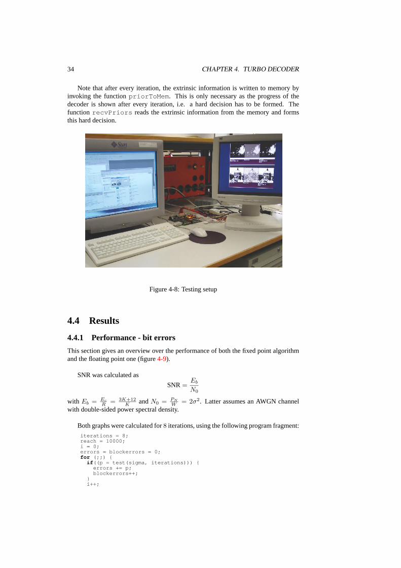
34 CHAPTER 4. TURBO DECODER
Note that after every iteration, the extrinsic information is written to memory byinvoking the functionpriorToMem . This is only necessary as the progress of thedecoder is shown after every iteration, i.e. a hard decision has to be formed. Thefunction recvPriors reads the extrinsic information from the memory and formsthis hard decision.
Figure 4-8: Testing setup
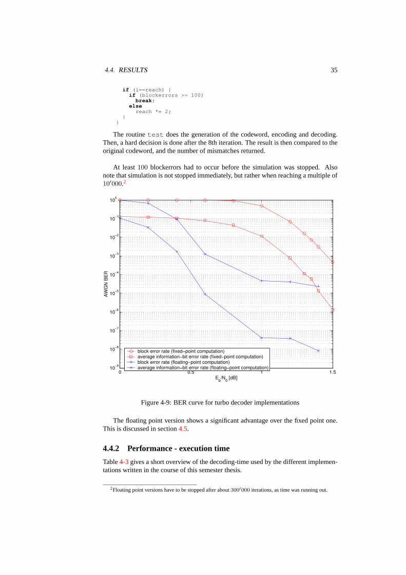
4.4 Results
4.4.1 Performance - bit errors
This section gives an overview over the performance of both the fixed point algorithmand the floating point one (figure4-9).
SNR was calculated as
SNR=Eb
N0
with Eb = Ec
R = 3K+12K andN0 = PN
W = 2σ2. Latter assumes an AWGN channelwith double-sided power spectral density.
Both graphs were calculated for8 iterations, using the following program fragment:
iterations = 8;reach = 10000;i = 0;errors = blockerrors = 0;for (;;) {
if ((p = test(sigma, iterations))) {errors += p;blockerrors++;
}i++;
4.4. RESULTS 35
if (i==reach) {if (blockerrors >= 100)
break ;else
reach *= 2;}
}
The routinetest does the generation of the codeword, encoding and decoding.Then, a hard decision is done after the 8th iteration. The result is then compared to theoriginal codeword, and the number of mismatches returned.
At least 100 blockerrors had to occur before the simulation was stopped. Alsonote that simulation is not stopped immediately, but rather when reaching a multiple of10′000.2
0 0.5 1 1.510−9
10−8
10−7
10−6
10−5
10−4
10−3
10−2
10−1
100
Eb/N
0 [dB]
AW
GN
BE
R
block error rate (fixed−point computation)average information−bit error rate (fixed−point computation)block error rate (floating−point computation)average information−bit error rate (floating−point computation)
Figure 4-9: BER curve for turbo decoder implementations
The floating point version shows a significant advantage over the fixed point one.This is discussed in section4.5.
4.4.2 Performance - execution time
Table4-3gives a short overview of the decoding-time used by the different implemen-tations written in the course of this semester thesis.
2Floating point versions have to be stopped after about300′000 iterations, as time was running out.

36 CHAPTER 4. TURBO DECODER
For testing purposes,10′000 random codewords (=6′125′000 bytes) were gener-ated and encoded. Then, the respective decoder implementation ran8 iterations on theencoded codeword.Please note that these numbers only give a rough idea of the performance—all imple-mentations can still be optimized.
Implementation Platform Time
Floating point AMD 1600XP 19 minFixed point AMD 1600XP 64 minFixed point 31 min
Table 4-3: Time used for decoding10′000 codewords
With the software version achieving a peak data rate of5.18 KB/s, none of theseimplementations are suitable for actual applications.Still, even at the modest clock rate of50 MHz, the hardware implementation almostreaches the performance of the significantly higher clocked PC version. In section4.5on page37, we suggest a few measures to gain enough speed for medium data rates.
4.4.3 ASIC
Without any doubt, a proprietary ASIC solution would be superior in speed, and evenmore in area and power consumption. But also FPGAs have their advantages:
• The manufacturing technology used for the Virtex2 FPGAs is0.13µm, currentdesigns even use0.09µm. This state of the art technology is normally not appliedto ASICSs which are produced in much lower quantities.
• An ASIC—in smaller quantities—is much more expensive than an FPGA. Addi-tionally, all possible options for varying block lengths and the like already haveto be hard-wired into the chip, which can increase the chip size significantly (as-suming similar interleaver tables as we used).For an FPGA, a mere resynthesis can adapt the decoder to another standard,eliminating the need for parts that allow the selection of different codes.
• In addition to this, with a system as the proposed RHWOS, it would be possibleto share the FPGA area with other processing tasks. This applies when the turbodecoder does not have to be available at all times, or can decode quickly enoughinto a buffer.
• Development of an FPGA system is easier, especially testing.
These points should be considered in the following sections when the weaknessesof FPGAs are discussed in more detail.
Execution time
Some parts of the FPGA work with optimal performance, e.g. multipliers and Block-RAM. The rest has quite a reasonable performance. Under the assumption that theVHDL code of the ASIC and the FPGA are more or less equivalent, the performancedrawback is most likely below a factor of4.

4.5. FURTHER STEPS 37
Other than that, the ASIC offers a lot more freedom concerning memory and multiplierelements. There are also fewer size restrictions. Therefore, it would be possible toimplement several decoders in parallel, each with its own onboard memory. In termsof clock rate, the differences are not notable. This holds true especially because of themore recent manufacturing technology.
Area usage
Normally, it is assumed that only 10% of the FPGA die is used for actual logic, the restis consumed by routing. Thus, an ASIC may be about 10 times smaller. But this is avery rough approxmation, depending on implementation and manufactoring technolgy.Another important point is the fixed size of an FPGA. As we use only 15% of the chip,we are certainly far away from an optimal space usage. As mentioned above, the restof the chip could be used for other tasks.
Power dissipation
Power dissipation heavily depends on the FPGA technology used. The Virtex2 workswith power consuming SRAM technology, whereas chips based on antifuse technol-ogy would be by far better. The disadvantage of the latter is that they can be configuredonly once, thus they were not suitable for this project.
Xilinx offers the tool XPower which calculates the actual power consumption of adesign. Due to lack of time, we could not test it. But the approximated overall powerconsumption of the FPGA may be around1′000 mW, with 500 mW being static powerconsumption, independent of the actual configuration of the chip.Again, an ASIC could be at least 10 times more efficient, probably even more.
4.5 Further steps
The aim of this project was to implement a turbo decoder on an FPGA. As only alimited amount of time was available, performance was not highest priority.The following chapter presents some ideas for possible improvements. They can beorganized into three parts: execution time, memory usage and decoding quality.
Memory usage
Currently, the memory usage of the decoder system is not optimal (approximately120kB are needed). Several steps can be taken to drastically whittle it down.
First, since the channel estimation is normalized to1, only half the information hasto be stored, as the other half can be calculated on the fly.
The same can be applied to the extrinsic information of the decoders when normal-izing it before sending it to the next decoder.
Also, it would be possible to abandon the space needed for the backward iteration’sstate metrics by calculating the extrinsic information during the backward iteration.In this implementation, SRAM had to be used anyway, so the simpler alternative of a
38 CHAPTER 4. TURBO DECODER
seperate calculation step for extrinsic information was chosen.
Finally, the current implementation overrides the least significant bit of the dataread in most cases. Thus, if the precision is satisfying,7 bit could be used instead of 8to represent the data.
Overall, forK = 4′900 and8 bit precision, a memory usage of63′744 bytes wouldthus suffice.
Execution time
The two main bottlenecks of the current architecture are memory bandwidth and theMicroblaze soft processor. Also, the forward-backward algorithm has some room forimprovements.
Concerning the Microblaze parts, not much can be done, except moving furtherparts to hardware or increasing the clockrate. Because of this, only improvements con-cerning the hardware part of the system are considered.
One iteration of the forward-backward algorithm takes approximately668′500 cy-cles3. 637′300 of these are used for accessing memory.The current memory interface is designed for simplicity rather than speed, taking be-tween4 and5 cycles per memory access.4 This figure could be reduced to2 cycles,thus yielding215′600 cycles in total - a speedup of
S =31′200 + 637′30031′200 + 215′600
= 2.71
This problem hopefully will be resolved by the further development of the RHWOSand an accompanying memory manager.
Also, using some sort of cache architecture, one could ensure that the memory isbusy all the time, saving some extra cycles. This turns out to be rather straight-forward,as the next value to be accessed is known in every step of the algorithm.Another possible solution to achieve constant usage of memory would be pipelining ofmemory loading, calculation and storage.
The weak point of the forward-backward algorithm is the scaling of the state met-rics. As of now, this is done in a loop that shifts all messages to the left by one bit untilthe most significant bit of one message is set.A parallel version could bring considerable speedup - the current maximum bit caneasily be found by ORing all the current state metrics. From this, the shift count canbe inferred and executed in a single cycle.
Furthermore, calculation of the extrinsic information is done in a seperate step. Byintegrating this into the backward iteration, one would not only require less memory forstoring the state metrics, but roughly, another98′000 cycles could be saved, resulting
3Based on simulating the behavioural model in ModelSim. This figure can vary depending on input.4The reason for this is a very simple request-acknowledge protocol used for communicating with the
memory manager.

4.5. FURTHER STEPS 39
in an overall speedup of5.17.
Summing up, at a clock rate of50 MHz, a run of a single decoder could be opti-mized to take2.5 ms instead of13.3 ms.
If the entire chip area of the Virtex2 FPGA could be used, and memory usage is op-timized as described above, internal BlockRAM could be used for all data. Accessingdata there only takes1 clock cycle, yielding a speedup of7.42 compared to the currentversion.
Of course, increasing to clock rate can also give a reduction in execution time.However, this is not advisable due to both increased power dissipation and the timingconstraints given by the external memory.
Numerical improvement
As mentioned above, the implementation presented here is working with fixed pointnumbers. This is not optimal for very noisy signals. Floating point arithmetic—or log-likelihood arithmetic—should yield a significant improvment in such situations. [8]gives a detailed analysis of the latter.The current implementation assumes 8 bit per probability. To accomodate for a largerrange, one byte could be splitted into a 5 bit mantissa and 3 bit exponent. Then, eachmultiplication needs a parallel addition for the exponents and an additional step torecombine the result.
RHWOS
At the time of writing, the RHWOS infrastructure was not ready yet. Thus, the turbodecoder presented here is still a stand-alone version, that has to be adapted slightly toactually become suitable as a task.Basically, the idea is to keep the actual decoder hardware on the R-FPGA, whereas thecontrolling Microblaze program has to be taken to the C-FPGA part of the system.
Most of these points also apply when porting the decoder to another platform uti-lizing Virtex2 FPGAs.
Communication Currently, the turbo decoder interfaces to the Microblaze via 3GPIO registers (input, output and control) that have to be replaced by the standardtask interface (STI).
The controlling program abstracts from these communications via the fileturbo.c .On the VHDL side,top.vhd is the interface to the turbo decoder - its signals have tobe routed to the STI.
Memory The turbo decoder accesses its data using the memory manager found inmemmanager.vhd , which in turn abstracts from the actual memory (in our applica-tion, the right SRAM bank of the ) using the filebasicmem.vhd .Addresses are generated bymemmanager.vhd , and at the very beginning of thearchitecture part of the file, a base address can be given. As stated above inthe memory section, a total of127′488 bytes are needed.

40 CHAPTER 4. TURBO DECODER
This memory manager has to be connected to the RHWOS’ memory manager,which handles concurrent accesses by the tasks to the SRAM. The interim solution,basicmem.vhd assumes the signals seen in table4-4 from the memory manager.
Signal Meaning
Addr 20 bit address for SRAMDataIn 16 bit data to be writtenDataOut 16 bit data read (registered)TRQ transaction requestACK acknowledge signalWEn write enable (high active)
Table 4-4: Ports for memory manager
4.6 Running the demo
4.6.1 Software needed
• Xilinx Project Navigator (ISE). This is used to compile the hardware part ofthe system.
• Xilinx Embedded Development Kit (EDK). Used to program the Microblazeprocessor in C.
• Microsoft Visual C. Used for the encoder application on the PC side.
4.6.2 Compiling the demo
Please refer to chapter6 on page45 concerning the location of the project files on theCD.
PC application
The PC application used to send packets over Ethernet is Microsoft Visual C project.Only the actual sending, and the displaying of the picture are platform dependent.The project file provided together with the source files contains all the dependencies,so executing the program from inside Visual C will do all the work needed.
XFBoard application
The application is split in both a hardware and a software part. Thus,compilation differs depending on where changes were applied.
Software Start EDK, and open the fileprojnav\system.xmp . Modificationsto the software part of the application can be applied here, and the finished projectdownloaded to the FPGA using the option Download Bitstream.

4.6. RUNNING THE DEMO 41
Hardware This has to be done in two steps:
1. Start ISE, and open the fileprojnav\system.npl . This project connectsthe hardware portion of the decoder to the Microblaze architecture. The option“Generate programming file” will prepare a.bit stream for the Microblazearchitecture
2. Start EDK, open the project filesystem.xmp and select the option “Importfrom ProjNav” to import the generated.bit stream, which is located in thedirectoryprojnav\system.bit .The .bmm file can be found inimplementation\system_bd.bmm .
After importing, the software will now work with the updated hardware part of thesystem.
IP Addresses
IP addresses are hard coded in both applications. The default IP addresses used cur-rently are169.254.45.1 for the PC, and169.254.45.2 for . As sending isonly done in one direction, only the address of the can be changed.
• PC.Change the variablem_IPAddressStr in TurboEncoderAppDlg.cpp
• XFBoard. Change the variableIPBoardAddress in network.c
4.6.3 Running the demo
Start EDK, open the filesystem.xmp . Select the option “Download” from the“Tools” menu to download the bitstream to the .The application will now poll the Ethernet and wait for the PC side to send an encodedblock (in13 packets). This block is then decoded and the progress of the turbo decodershown on screen.

42 CHAPTER 4. TURBO DECODER
Chapter 5
Conclusion
This semester thesis concentrated on the R-FPGA part of the .Both a device driver for the OS frame, as well as two signal processing tasks wereimplemented.
An overview over turbo codes is given, with references to papers concerning thesubject. In the implementation section, issues in bringing the design to hardware areanalyzed. Specifically, the translation to fixed-point arithmetics is described, alongwith a few solutions to prevent numerical underflows.
Then, an actual hardware version for the is presented. It’s used in atesting environment that receives encoded, noisy data from a PC and decodes it. Fi-nally, some results pertaining execution time and performance are shown.
While the turbo decoder implemented in the scope of this thesis is not useable in areal-world scenario, measures are suggested that could yield a significant performanceboost. This should be sufficient for medium data rates.Especially the aspect of using reconfigureable hardware for such a decoder seemstempting, and in comparison to proprietary ASIC solutions, a few promising aspectsare hinted at.
43

44 CHAPTER 5. CONCLUSION
Chapter 6
CD
This chapter gives a quick overview over the directory structure of the accompanyingCD.
• PresentationsSlides from the two presentations held
• Report Final version of this report, including all pictures
• SpectrumAnalyzerFiles for spectrum analyzer task
• TestProjectsVarious test projects
– MemTestTest for turbo decoder’s memory manager (right SRAM bank)
• TurboDecoder: directory of turbo decoder project, including all PC software
– Software
∗ InterleaverConstantGeneratorGenerates constants for the hardwareversion of the interleaver
∗ TurboEncoderApp Windows applications used in our testing envi-ronment to send an encoded, noisy picture to the .
∗ SNR_FixedPointSNR test for fixed point software implementation ofturbo decoder. Use “make” to compile.
∗ SNR_FloatingPoint SNR test for floating point software implemen-tation of turbo decoder. Use “make” to compile.
– TurboDecoderTurbo decoder hardware project.
• VGADriver Files for the VGA driver project
– VGADriver Actual VGA driver - files need
– VGADemo Demo as described in section2.10on page12
– VGAMicroblaze Demo for the Microblaze part of the VGA driver
45

46 CHAPTER 6. CD
Bibliography
[1] Alliance Semiconductor.AS7C4096/ AS7C34096, 5V/3.3V 52K x 8 CMOS SRAM,March 2002, v.1.8.http://www.alsc.com/pdf/sram.pdf/fa/AS7C34096.pdf
[2] L. Bahl, J. Cocke, F. Jelinek and J. Raviv.Optimal decoding of linear codes forminimizing symbol error rate, IEEE trans. Inf. Theory, March 1974, pp. 284-287.
[3] C. Berrou, A. Glavieux., and P. Thitimajshima.Near Shannon Limit Error-Correcting Coding and Decoding: Turbo Codes, IEEE Proc. ICC ’93, Geneva,Switzerland, May 1993, pp. 1064-1070.
[4] ETSI. Universal Mobile Telecommunications System (UMTS); Multiplexing andchannel coding (FDD) (3GPP TS 25.212 version 3.4.0 Release 1999)
[5] Intersil Corporation.HI1178 Triple 8-bit, 40MSPS, RGB, 3-Channel D/A Con-verter, 2000.http://www.intersil.com/design/images/DataSheet.jpg
[6] H.-A. Loeliger. Stochastische Modelle und Signalverarbeitung, Lecture Notes,ETH Zurich, winter term 2003.
[7] M. Matsumoto and T. Nishimura.Mersenne Twister: A 623-dimensionallyequidistributed uniform pseudorandom number generator, ACM Transactions onModeling and Computer Simulation Vol. 8, No. 1, January 1998, pp. 3-30.
[8] G. Montorsi, and S. Benedetto.Design of Fixed-Point Iterative Decoders for Con-catenated Codes with InterleaversIEEE Journal on selected areas in communi-cations, vol. 19, no. 5, May 2001, pp. 871-882.
[9] S. Nobs. Student Thesis, Swiss Federal Institute of Technology Zurich (ETH),Computer Engineering and Networks Laboratory.Prototype Board for Reconfig-urable OS, July 2003.http://www.tik.ee.ethz.ch/∼walder/HomePage/SADA/PrototypeBoardForReconfigurableOS/PBFROS.pdf
[10] S. Nobs. Diploma Thesis, Swiss Federal Institute of Technology Zurich (ETH),Computer Engineering and Networks Laboratory.Reconfigurable Hardware OS- Prototype Part "C", 2004.
[11] B. Sklar.A Primer on Turbo Code Concepts, IEEE Communications Magazine,December 1997, pp. 94-102.
47

48 BIBLIOGRAPHY
[12] S. Steinegger. Diploma Thesis, Swiss Federal Institute of Technology Zurich(ETH), Computer Engineering and Networks Laboratory.Reconfigurable Hard-ware OS - Prototype Part “FPGA”, 2004.
[13] VGA timing information, http://www.epanorama.net/documents/pc/vga_timing.html
[14] H. Walder, M. Platzner. Swiss Federal Institute of Technology Zurich (ETH),Computer Engineering and Networks Laboratory, TIK Report Nr. 168.Reconfig-urable Hardware OS Prototype, April 2003.http://www.tik.ee.ethz.ch/∼walder/XFORCES/TIKR168.pdf
[15] S. Wegmann. Diploma Thesis, Swiss Federal Institute of Technology Zurich(ETH), Computer Engineering and Networks Laboratory.Video Playback Tasksfor RHWOS, 2004.
[16] Xilinx, Inc. Virtex-II Platform FPGAs: Advance Product Specification, 2002.http://direct.xilinx.com/bvdocs/publications/ds031.pdf
[17] Xilinx, Inc. Virtex-II Platform FPGA User Guide, December 2002.http://www.xilinx.com/publications/products/v2pro/ug_pdf/ug012.pdf
[18] Xilinx, Inc. MicroBlaze RISC 32-Bit Soft Processor, August 2001.http://www.xilinx.com/ipcenter/catalog/logicore/docs/microblaze_risc_32bit_proc_final.pdf
[19] Xilinx, Inc.http://www.xilinx.com
[20] Xilinx, Inc.http://www.xilinx.com/ipcenter/catalog/logicore/docs/xfft.pdf
Please note that the URLs noted below the reference entries have been valid at thetime of writing. However, they may have become outdated in the meantime.
6th February 2004