andrew kahng – march 2002 design-process integration and shared red bricks dpimm-02 invited talk...
Post on 21-Dec-2015
212 views
TRANSCRIPT

Andrew Kahng – March 2002
Design-Process Integration and Shared Red Bricks
DPIMM-02 Invited TalkMarch 6, 2002
Andrew B. Kahng, UCSD CSE & ECE Departmentsemail: [email protected]: http://vlsicad.ucsd.edu

Andrew Kahng – March 2002
OutlineOutline
• 1. Background: ITRS and system drivers• 2. Design roadmap• 3. On the Design Productivity Gap• 4. Sharing red bricks• 5. Design-manufacturing integration• 6. Conclusion

Andrew Kahng – March 2002
The “Red Brick Wall” - 2001 ITRS vs 1999
Source: Semiconductor International - http://www.e-insite.net/semiconductor/index.asp?layout=article&articleId=CA187876

Andrew Kahng – March 2002
Acceleration/Deceleration = Balancing Act
Year of Production: 1999 2002 2005 2008 2011 2014
DRAM Half-Pitch [nm]: 180 130 100 70 50 35
Overlay Accuracy [nm]: 65 45 35 25 20 15
MPU Gate Length [nm]: 140 85-90 65 45 30-32 20-22
CD Control [nm]: 14 9 6 4 3 2
TOX (equivalent) [nm]: 1.9-2.5 1.5-1.9 1.0-1.5 0.8-1.2 0.6-0.8 0.5-0.6
Junction Depth [nm]: 42-70 25-43 20-33 16-26 11-19 8-13
Metal Cladding [nm]: 17 13 10 000
Inter-Metal Dielectric 3.5-4.0 2.7-3.5 1.6-2.2 1.5
2001 versus 1999 Results
Source: A. Allan, Intel

Andrew Kahng – March 2002
Design ITWG Contributions to ITRS-2001Design ITWG Contributions to ITRS-2001
• New System Drivers Chapter
• Design Chapter
• ORTC support– Frequency– Power– Density
• New design cost and productivity models
Andrew Kahng – March 2002
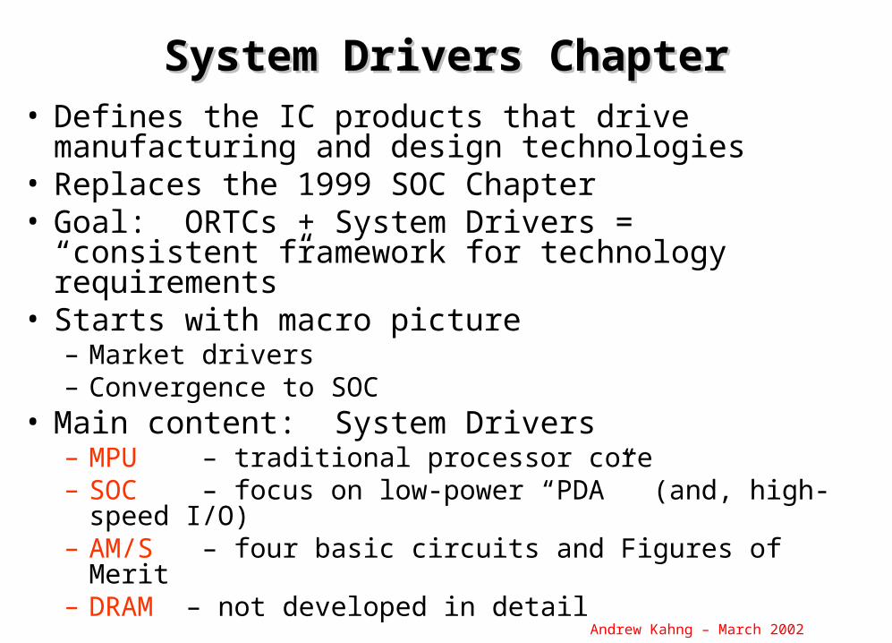
System Drivers ChapterSystem Drivers Chapter• Defines the IC products that drive manufacturing
and design technologies• Replaces the 1999 SOC Chapter• Goal: ORTCs + System Drivers = “consistent
framework for technology requirements”• Starts with macro picture
– Market drivers– Convergence to SOC
• Main content: System Drivers – MPU – traditional processor core– SOC – focus on low-power “PDA” (and, high-speed I/O)– AM/S – four basic circuits and Figures of Merit– DRAM – not developed in detail
Andrew Kahng – March 2002
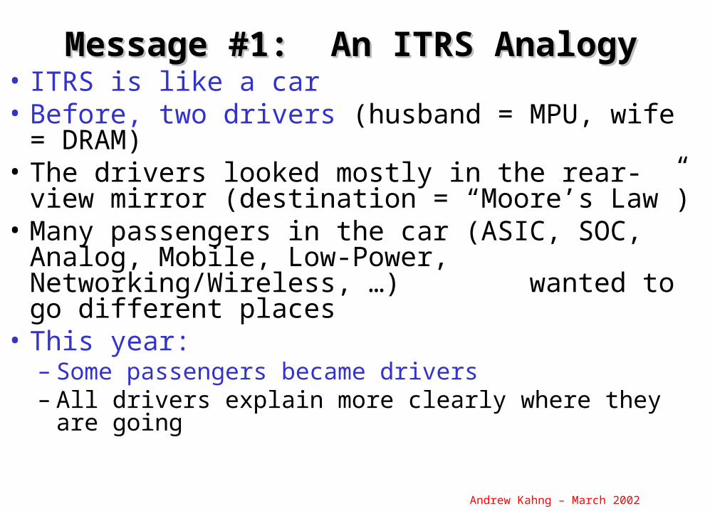
Message #1: An ITRS AnalogyMessage #1: An ITRS Analogy• ITRS is like a car• Before, two drivers (husband = MPU, wife =
DRAM)• The drivers looked mostly in the rear-view mirror
(destination = “Moore’s Law”)• Many passengers in the car (ASIC, SOC, Analog,
Mobile, Low-Power, Networking/Wireless, …) wanted to go different places
• This year: – Some passengers became drivers– All drivers explain more clearly where they are going

Andrew Kahng – March 2002
OutlineOutline
• 1. Background: ITRS and system drivers• 2. Design roadmap• 3. On the Design Productivity Gap• 4. Sharing red bricks• 5. Design-manufacturing integration• 6. Conclusion
Andrew Kahng – March 2002
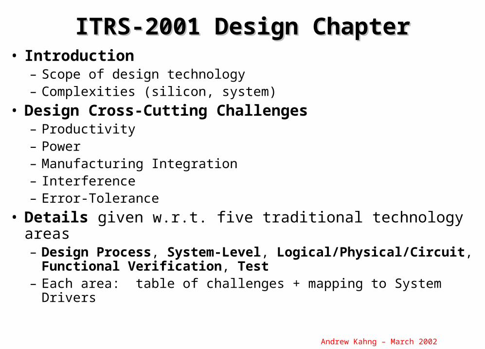
ITRS-2001 Design ChapterITRS-2001 Design Chapter• Introduction
– Scope of design technology– Complexities (silicon, system)
• Design Cross-Cutting Challenges– Productivity– Power– Manufacturing Integration– Interference– Error-Tolerance
• Details given w.r.t. five traditional technology areas– Design Process, System-Level, Logical/Physical/Circuit,
Functional Verification, Test– Each area: table of challenges + mapping to System Drivers

Andrew Kahng – March 2002
Silicon Complexity ChallengesSilicon Complexity Challenges• Silicon Complexity = impact of process scaling, new materials,
new device/interconnect architectures• Non-ideal scaling (leakage, power management, circuit/device
innovation, current delivery)• Coupled high-frequency devices and interconnects (signal
integrity analysis and management)• Manufacturing variability (library characterization, analog and
digital circuit performance, error-tolerant design, layout reusability, static performance verification methodology/tools)
• Scaling of global interconnect performance (communication, synchronization)
• Decreased reliability (SEU, gate insulator tunneling and breakdown, joule heating and electromigration)
• Complexity of manufacturing handoff (reticle enhancement and mask writing/inspection flow, manufacturing NRE cost)

Andrew Kahng – March 2002
System Complexity ChallengesSystem Complexity Challenges• System Complexity = exponentially increasing transistor
counts, with increased diversity (mixed-signal SOC, …)• Reuse (hierarchical design support, heterogeneous SOC
integration, reuse of verification/test/IP)• Verification and test (specification capture, design for
verifiability, verification reuse, system-level and software verification, AMS self-test, noise-delay fault tests, test reuse)
• Cost-driven design optimization (manufacturing cost modeling and analysis, quality metrics, die-package co-optimization, …)
• Embedded software design (platform-based system design methodologies, software verification/analysis, codesign w/HW)
• Reliable implementation platforms (predictable chip implementation onto multiple fabrics, higher-level handoff)
• Design process management (team size / geog distribution, data mgmt, collaborative design, process improvement)

Andrew Kahng – March 2002
SOC Design Cost Model
$3
42
,41
7,5
79
$1
5,0
66
,37
3
$10,000,000
$100,000,000
$1,000,000,000
$10,000,000,000
$100,000,000,000
1985 1990 1995 2000 2005 2010 2015 2020Year
To
tal D
esig
n C
ost
(l
og
sca
le)
RTL Methodology Only
With all Future Improvements
In-H
ouse
P&
R
Tal
l Thi
n E
ngin
eer
Sm
all B
lock
Reu
se
IC Im
plem
enta
tion
tool
s
Larg
e B
lock
Reu
se
Inte
lligen
t Tes
tben
ch
ES
Lev
el M
etho
dolo
gy
Design Cost of ITRS SOC-LP PDA Driver
Andrew Kahng – March 2002
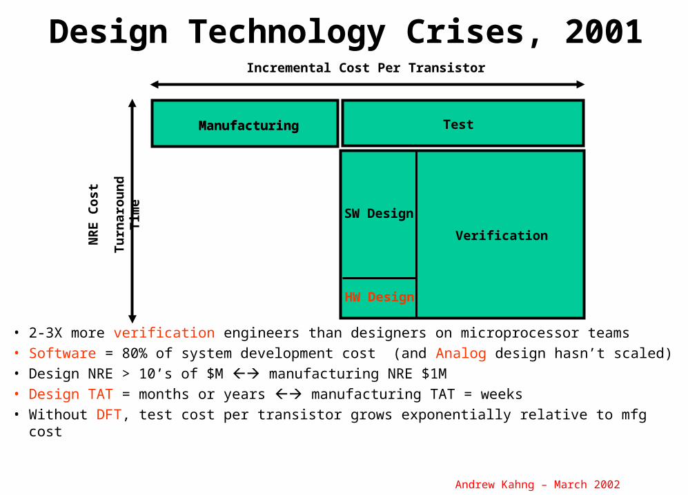
Design Technology Crises, 2001
Manufacturing
NR
E C
ost
SW Design
Verification
HW Design
TestT
urn
aro
un
d T
ime
Manufacturing
Incremental Cost Per Transistor
• 2-3X more verification engineers than designers on microprocessor teams
• Software = 80% of system development cost (and Analog design hasn’t scaled)
• Design NRE > 10’s of $M manufacturing NRE $1M
• Design TAT = months or years manufacturing TAT = weeks
• Without DFT, test cost per transistor grows exponentially relative to mfg cost
Andrew Kahng – March 2002
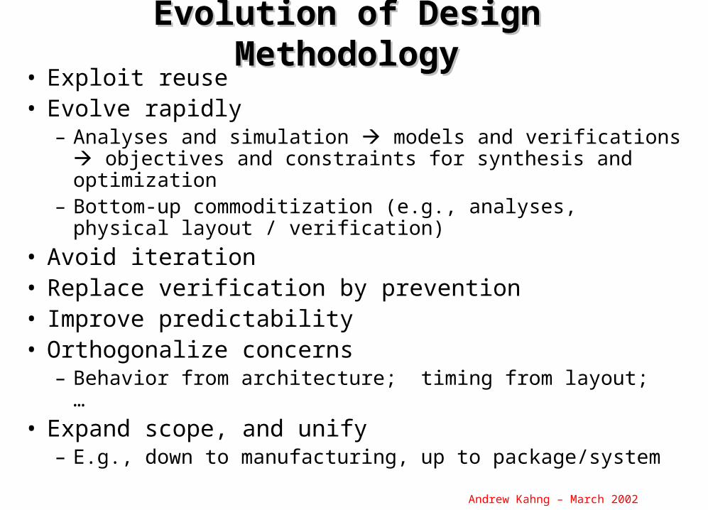
Evolution of Design MethodologyEvolution of Design Methodology• Exploit reuse• Evolve rapidly
– Analyses and simulation models and verifications objectives and constraints for synthesis and optimization
– Bottom-up commoditization (e.g., analyses, physical layout / verification)
• Avoid iteration• Replace verification by prevention• Improve predictability• Orthogonalize concerns
– Behavior from architecture; timing from layout; …
• Expand scope, and unify– E.g., down to manufacturing, up to package/system

Andrew Kahng – March 2002
Message #2: Design Big PictureMessage #2: Design Big Picture• Cost of Design threatens continuation of the
semiconductor roadmap– New Design cost model– Challenges are now Crises

Andrew Kahng – March 2002
OutlineOutline
• 1. Background: ITRS and system drivers• 2. Design roadmap• 3. On the Design Productivity Gap• 4. Sharing red bricks• 5. Design-manufacturing integration• 6. Conclusion

Andrew Kahng – March 2002
Productivity Gap (1994)
Equivalent Added Complexity
68 %/Yr compoundedComplexity growth rate
21 %/Yr compoundProductivity growth rate
Year Technology Chip Complexity Frequency Staff Staff Cost* 3 Yr. Design
1997 250 nm 13 M Tr. 400 MHz 210 90 M
1998 250 nm 20 M Tr. 500 270 120 M
1999 180 nm 32 M Tr. 600 360 160 M
2002 130 nm 130 M Tr. 800 800 360 M
* @ $ 150 k / Staff Yr. (In 1997 Dollars)
Logic Tr./Chip Tr./S.M.
Source: SEMATECHSource: SEMATECH
Potential Design Complexity and Designer Productivity

Andrew Kahng – March 2002
Mask NRE Cost (1999 Sematech)
“$1M mask set” in 100nm, but average only 500 wafers per set
Andrew Kahng – March 2002
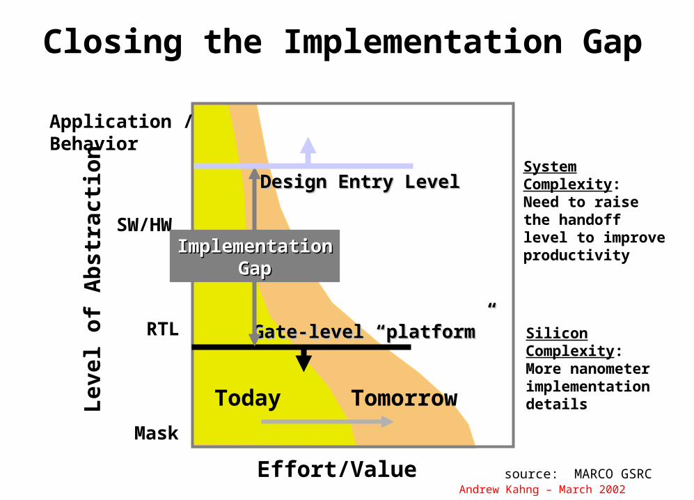
Closing the Implementation Gap
Effort/Value
Leve
l of A
bstr
actio
n
RTL
Mask
Application /Behavior
SW/HW
Gate-level “platform”Gate-level “platform”
ImplementationImplementationGapGap
Design Entry LevelDesign Entry Level
Today Tomorrow
source: MARCO GSRC
System Complexity: Need to raise the handoff level to improve productivity
Silicon Complexity: More nanometer implementation details
Andrew Kahng – March 2002
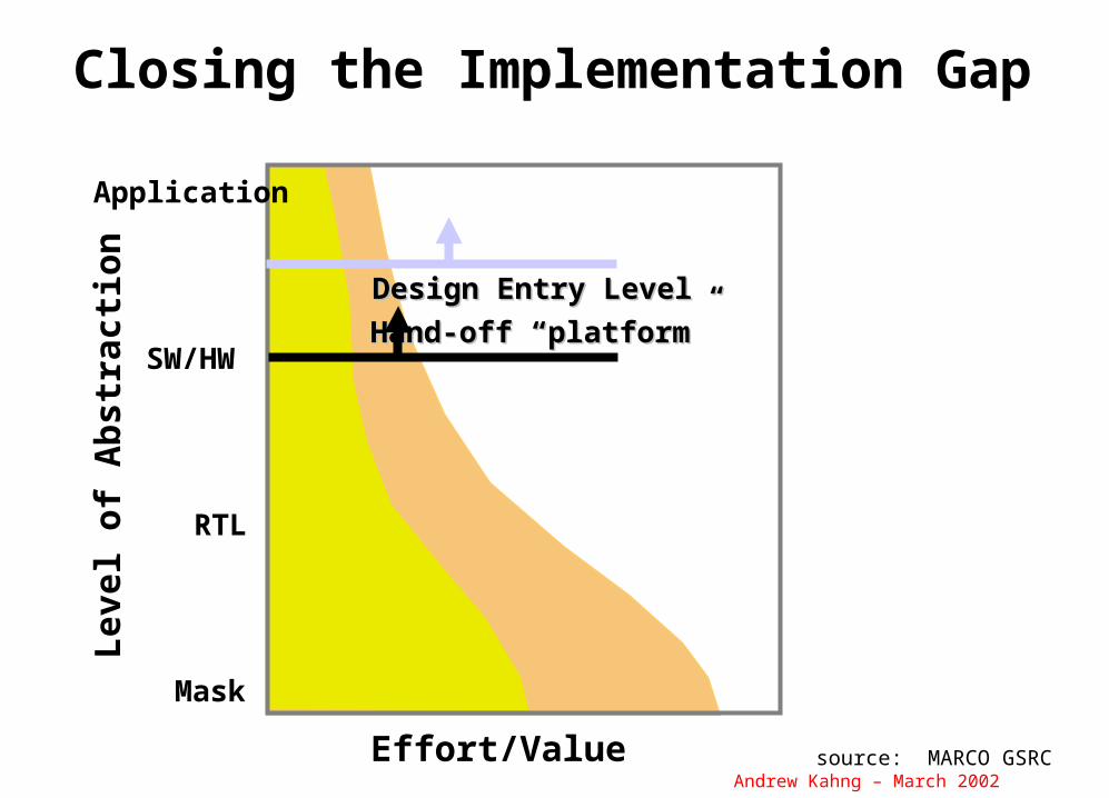
Closing the Implementation Gap
Effort/Value
Leve
l of A
bstr
actio
n
RTL
Mask
Application
SW/HWHand-off “platform”Hand-off “platform”
Design Entry LevelDesign Entry Level
source: MARCO GSRC

Andrew Kahng – March 2002
0%
20%
40%
60%
80%
100%
1999
2002
2005
2008
2011
2014
% Area Memory
% Area ReusedLogic
% Area New Logic
Percent of die area that must be occupied by memory to maintain SOC design productivity (or, power for that matter)(STRJ-WG1 analysis, published in ITRS-2000 / ITRS-2001)
Low-Value Designs?Low-Value Designs?
An all-memory design is probably a low-value design

Andrew Kahng – March 2002
Reduced Back-End Effort ?
Example: regular shieldedExample: regular shielded wiring fabricwiring fabricpattern at minimum pitchpattern at minimum pitch
S SV V SG
SG
SSV
V
SS SSVV VV SSGG
- Eliminates signal integrity, delay uncertainty concerns- But has at least 60% - 80% density cost
source: MARCO GSRC

Andrew Kahng – March 2002
Improved Reuse Productivity ?
MacroShells (the Protocol Interface)Communication Channels
MicroShells (the IP Requirements)
P1
P2
P3
P4
P5
P6
P7
Pearls (the IP Processes)
source: MARCO GSRC
Example: “communication-based design”Example: “communication-based design”
Andrew Kahng – March 2002
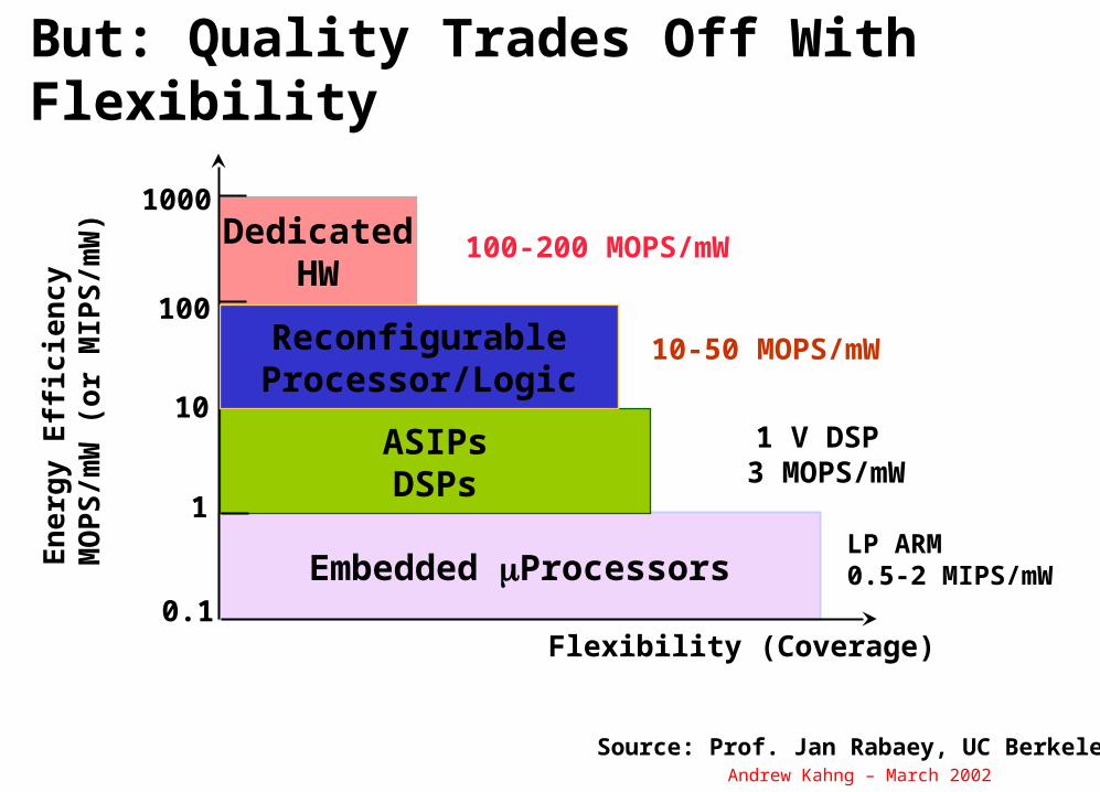
Embedded ProcessorsLP ARM0.5-2 MIPS/mW
ASIPsDSPs
1 V DSP 3 MOPS/mW
But: Quality Trades Off With Flexibility
DedicatedHW
Flexibility (Coverage)
En
ergy
Eff
icie
ncy
MO
PS
/mW
(or
MIP
S/m
W)
0.1
1
10
100
1000
ReconfigurableProcessor/Logic
10-50 MOPS/mW
100-200 MOPS/mW
Source: Prof. Jan Rabaey, UC Berkeley
Andrew Kahng – March 2002
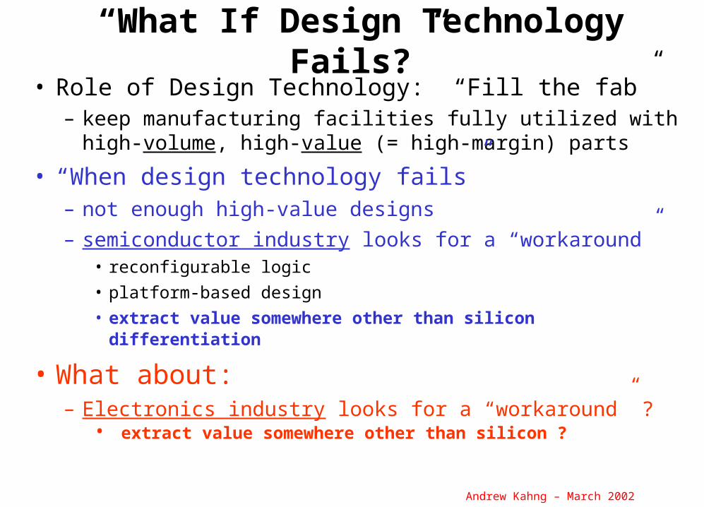
“What If Design Technology Fails?”• Role of Design Technology: “Fill the fab”
– keep manufacturing facilities fully utilized with high-volume, high-value (= high-margin) parts
• “When design technology fails”– not enough high-value designs
– semiconductor industry looks for a “workaround”• reconfigurable logic
• platform-based design
• extract value somewhere other than silicon differentiation
• What about:– Electronics industry looks for a “workaround” ?
• extract value somewhere other than silicon ?

Andrew Kahng – March 2002
So: Design / Manufacturing In Same Boat• Design productivity is a determinant of how
efficiently we extract value from manufacturing capability
• Design productivity gap threatens design quality• #Design starts, business models at risk
– More reprogrammable, platform-based “workarounds”– More software workarounds
Why retool?• How much of your system is: Random logic? Pad-
limited? Time-to-market-limited? Verification-, software-, analog-, … limited? Hard cost-limited?

Andrew Kahng – March 2002
Message #3: Manufacturing Needs Message #3: Manufacturing Needs to Care About Designto Care About Design
• “Number of available transistors grows faster than designer ability to design them well” Increased design effort, risk, turnaround time (TAT)
fewer designs are worth trying• Manufacturing non-recurring engineering (NRE)
cost (mask set, probe card) are increasing fewer designs are worth trying
• “Workarounds” sacrifice quality, value of designs even with workarounds, fewer designs worth trying
• This is a semiconductor industry problem, not an EDA (“design productivity gap”) problem

Andrew Kahng – March 2002
OutlineOutline
• 1. Background: ITRS and system drivers• 2. Design roadmap• 3. On the Design Productivity Gap• 4. Sharing red bricks• 5. Design-manufacturing integration• 6. Conclusion
Andrew Kahng – March 2002
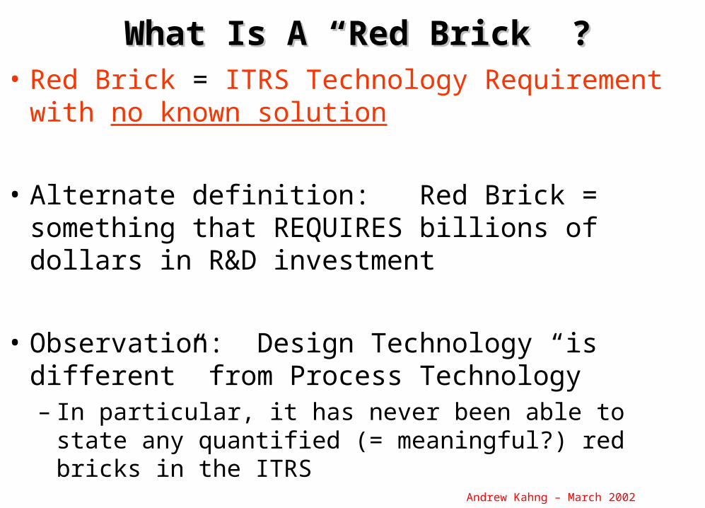
What Is A “Red Brick” ?What Is A “Red Brick” ?• Red Brick = ITRS Technology Requirement with
no known solution
• Alternate definition: Red Brick = something that REQUIRES billions of dollars in R&D investment
• Observation: Design Technology “is different” from Process Technology– In particular, it has never been able to state any
quantified (= meaningful?) red bricks in the ITRS

Andrew Kahng – March 2002
My “Big Picture”My “Big Picture”• Why ITRS has “red brick” problems
– “Wrong” Moore’s Law• Frequency and bits are not the same as efficiency and utility• No awareness of applications or architectures (only Design is aware)
– Independent, “linear” technological advances don’t work– No clear ground rules
• E.g., is cost a consideration? Is the Roadmap only for planar CMOS?
• New in 2001: Everyone asks “Can Design help us?”– Process Integration, Devices & Structures (PIDS): 17%/year
improvement in CV/I metric punt Ioff, Rds, …analog, LOP, LSTP, … many flavors
– Assembly and Packaging: cost limits keep bump pitches high punt IR drop, signal integrity (impacts Test as well)
– Interconnect, Lithography, PIDS/Front-End Processes: What variability can Designers tolerate? 10%? 15%? 25%?

Andrew Kahng – March 2002
YEAR
TECHNOLOGY NODE
2001 2002 2003 2004 2005 2006 2007
DRAM ½ PITCH (nm) (SC. 2.0) 130 115 100 90 80 70 65
MPU/ASIC ½ PITCH (nm) (SC. 3.7) 150 130 107 90 80 70 65
MPU PRINTED GATE LENGTH (nm) (SC. 3.7) 90 75 65 53 45 40 35
MPU PHYSICAL GATE LENGTH (nm) (SC. 3.7) 65 53 45 37 32 28 25
Conductor effective resistivity(-cm) Cu intermediate wiring*
2.2 2.2 2.2 2.2 2.2 2.2 2.2
Barrier/cladding thickness(for Cu intermediate wiring) (nm)
18 15 13 11 10 9 8
Interlevel metal insulator—effective dielectric constant ()
3.0-3.7 3.0–3.7 2.9–3.5 2.5–3.0 2.5–3.0 2.5–3.0 2.0–2.5
Interlevel metal insulator (minimumexpected)—bulk dielectric constant ()
2.7 2.7 2.7 2.2 2.2 2.2 1.7
Example Red Brick: Dielectric Permittivity
Bulk and effective dielectric constants
Porous low-k requires alternative planarization solutions
Cu at all nodes - conformal barriersC. Case, BOC Edwards – ITRS-2001 preliminary
Do we really need
this?
Andrew Kahng – March 2002
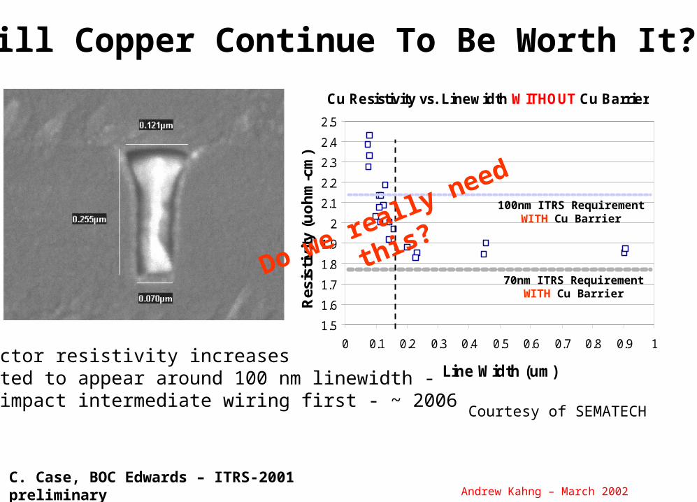
Cu Resistivity vs. Linewidth WITHOUT Cu Barrier
1.5
1.6
1.7
1.8
1.9
2
2.1
2.2
2.3
2.4
2.5
0 0.1 0.2 0.3 0.4 0.5 0.6 0.7 0.8 0.9 1
Line Width (um)
Res
isti
vity
(u
oh
m-c
m)
70nm ITRS RequirementWITH Cu Barrier
100nm ITRS RequirementWITH Cu Barrier
Will Copper Continue To Be Worth It?
Courtesy of SEMATECH
Conductor resistivity increasesexpected to appear around 100 nm linewidth -will impact intermediate wiring first - ~ 2006
C. Case, BOC Edwards – ITRS-2001 preliminary
Do we really need
this?

Andrew Kahng – March 2002
Cost of Manufacturing Test
Is this better solved with Automated Test Equipment technology, or with Design (for Test, Built-In Self-Test) ?
Is this even solvable with ATE technology alone?

Andrew Kahng – March 2002
Message #4Message #4• ITRS technologies are like parts of the ITRS car• Every one (= each ITRS chapter) takes the
“engine” point of view when it defines its requirements– “Why, you may take the most gallant sailor, the most intrepid airman, the
most audacious soldier, put them at a table together – what do you get? The sum of their fears.” - Winston Churchill
• All parts must work together to make the car go smoothly
• (Comment: Design = Steering wheel and/or tires … but has never “squeaked” loudly enough)
• The ITRS balancing act should entail global optimization” of requirements
Andrew Kahng – March 2002
And Hold This Thought…And Hold This Thought…• EDA as an industry:
– One chapter out of 12 in ITRS– One part of SISA – Small: 6000 R&D worldwide, $4B total market
• EDA growth rate, business model, research investment level are all laughable– Dataquest: 3.9% annual growth in tools $ spent per
designer– Pure research investment: few 10’s of $M per year– Tool integration costs >> tool costs– Vicious cycle of small ROI, small valuation, small size
• Yet, in 2001: “Can Design help us?”– This isn’t sharing red bricks – it’s punting red bricks

Andrew Kahng – March 2002
OutlineOutline
• 1. Background: ITRS and system drivers• 2. Design roadmap• 3. On the Design Productivity Gap• 4. Sharing red bricks• 5. Design-manufacturing integration• 6. Conclusion

Andrew Kahng – March 2002
ITRS-2001 Design ChapterITRS-2001 Design Chapter• Introduction
– Scope of design technology– Complexities (silicon, system)
• Design Cross-Cutting Challenges– Productivity– Power
–Manufacturing Integration– Interference– Error-Tolerance
• Details given w.r.t. five traditional technology areas– Design Process, System-Level, Logical/Physical/Circuit,
Functional Verification, Test– Each area: table of challenges + mapping to System Drivers

Andrew Kahng – March 2002
““Design-Manufacturing Integration”Design-Manufacturing Integration”• 2001 ITRS Design Chapter: “Manufacturing
Integration” = one of five Cross-Cutting Challenges
• Goal: share red bricks with other ITRS technologies– Lithography CD variability requirement new Design
techniques that can better handle variability
– Mask data volume requirement solved by Design-Mfg interfaces and flows that pass functional requirements, verification knowledge to mask writing and inspection
– Does “X initiative” have as much impact as copper?
– What is the cost/benefit of PhasePhirst! (on-grid layout)?
– So many opportunities!

Andrew Kahng – March 2002
PIDS (Devices/Structures)PIDS (Devices/Structures)
• CV/I trend (17% per year improvement) = “constraint”• Huge increase in subthreshold Ioff
– Room temperature: increases from 0.01 uA/um in 2001 to 10 uA/um at end of ITRS (22nm node)
• At operating temperatures (100 – 125 deg C), increase by 15 - 40x
– Standby power challenge• Manage multi-Vt, multi-Vdd, multi-Tox in same core• Aggressive substrate biasing• Constant-throughput power minimization• Modeling and controls passed to operating system and applications
• Aggressive reduction of Tox– Physical Tox thickness < 1.4nm (down to 1.0nm) starting in
2001, even if high-k gate dielectrics arrive in 2004– Variability challenge: “10%” < one atomic monolayer

Andrew Kahng – March 2002
LithographyLithography• 10% CD uniformity is a red brick today• 10% < 1 atomic monolayer at end of ITRS• This year: Lithography, PIDS, FEP agreed to raise CD
uniformity requirement to 15% (but still a red brick)• Design for variability
– Novel circuit topologies that are less sensitive to variations– Circuit optimization (conflict between slack minimization and
guardbanding of quadratically increasing delay sensitivity)– Statistical performance analysis flows– Centering and design for $/wafer– Highly constrained layouts (phase, orientation, pitch, …)
• Design for when devices, interconnects no longer 100% guaranteed correct?

Andrew Kahng – March 2002
Shared Red Bricks for Mask Handoff• WYSIWYG broken (mask) verification bottleneck
– Affects manufacturing NRE in mask, ASIC industries• Need function- and cost-aware OPC, PSM, dummy fill
– Real goal = predictable circuit performance and function– Therefore, tools must understand functional intent
• make only corrections that gain $$$, reduce performance variation• make only corrections that can be manufactured and verified (including mask inspection)• understand (data volume, verification) costs of breaking hierarchy
– Understand flow issues• e.g., avoid making same corrections 3x (library, router, PV tool)
• Need much more than GDSII in manufacturing interface– Includes sensitivities to patterning variation / error– Guided by models of manufacturing equipment – Mask verification needs to know same function, sensitivity info

Andrew Kahng – March 2002
Message #5A: We know this alreadyMessage #5A: We know this already
• Design KNOWS about these problems
• Design would like to IGNORE them
• Design can’t AFFORD to care about them (we have bigger fish to fry)

Andrew Kahng – March 2002
(1998) Problem Statements V• Pass functional intent down to OPC insertion
– OPC insertion is for predictable circuit performance, function
– Problem: make only corrections that win $$$, reduce perf variation (i.e., link to performance analysis, optimizations and sensitivities)
• Pass limits of mask verification up to layout– Problem: avoid making corrections that can’t be
manufactured or verified
• // I.e., 2-way fat pipe between process and design !– SPICE models are not a sufficient process abstraction…

Andrew Kahng – March 2002
(1998) Problem Statements VI• Minimize data volume
– Problem: make corrections that win $$$, reduce perf variation up to some limit of data volume for resulting layout (== mask complexity, cost)
• Layout needs models of OPC insertion process– Problem: taxonomize implications of layout geometry
on cost of the OPC that is required to yield function or “faithfully” print the geometry
– find a realistic cost model for breaking hierarchy (including verification, characterization costs)
Andrew Kahng – March 2002
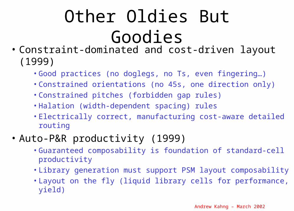
Other Oldies But Goodies• Constraint-dominated and cost-driven layout (1999)
• Good practices (no doglegs, no Ts, even fingering…)
• Constrained orientations (no 45s, one direction only)
• Constrained pitches (forbidden gap rules)
• Halation (width-dependent spacing) rules
• Electrically correct, manufacturing cost-aware detailed routing
• Auto-P&R productivity (1999)• Guaranteed composability is foundation of standard-cell
productivity
• Library generation must support PSM layout composability
• Layout on the fly (liquid library cells for performance, yield)

Andrew Kahng – March 2002
Other Oldies But Goodies• Sane RCX / PA flow with respect to area fill (1998)
• Area fill breaks RCX extraction• Must be modeled / predicted at timing / signal integrity signoff during auto-
P&R• Tradeoffs and correct models (grounded vs. ungrounded; synergies between fill
and printability (as opposed to planarization) must be understood
• PSM, OPC (?) and Fill must be owned by physical design, not physical verification (1999)
• PV tools have Boolean, purely geometric infrastructure• PV tools report errors (e.g., phase conflict), but are not empowered to fix (e.g.,
shift/compact layout
• Miscellaneous (1998)• Hierarchy, data volume, reuse concerns• New tool integrations: compaction, on-the-fly cell synthesis, incremental
detailed routing, graph-based (verification-type) layout analyses, performance and logic optimizations

Andrew Kahng – March 2002
So… How to Share Red Bricks?So… How to Share Red Bricks?
• Cost is the biggest missing link within the ITRS– Manufacturing cost (silicon cost per transistor)– Manufacturing NRE cost (mask, probe card, …)– Design NRE cost (engineers, tools, integration, …)– Test cost– Technology development cost who should solve a given
red brick wall?
• Return On Investment (ROI) = Value / Cost– Value needs to be defined (“design quality”, “time-to-market”)
• Understanding cost and ROI allows sensible levels of investment in, and sharing of red bricks across, the semiconductor supplier industries
Andrew Kahng – March 2002
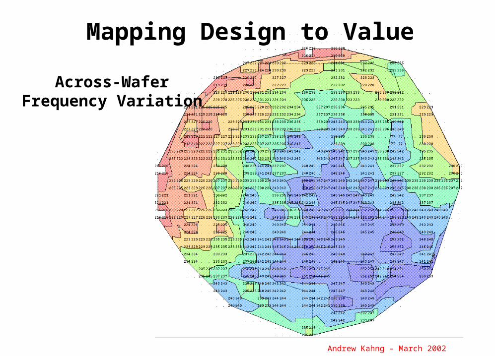
Mapping Design to Value
Across-Wafer Frequency Variation
Andrew Kahng – March 2002
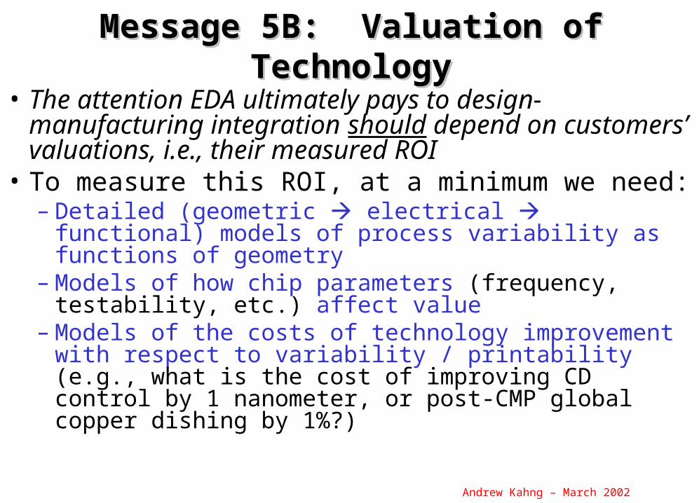
Message 5B: Valuation of TechnologyMessage 5B: Valuation of Technology
• The attention EDA ultimately pays to design-manufacturing integration should depend on customers’ valuations, i.e., their measured ROI
• To measure this ROI, at a minimum we need:– Detailed (geometric electrical functional) models
of process variability as functions of geometry – Models of how chip parameters (frequency, testability,
etc.) affect value– Models of the costs of technology improvement with
respect to variability / printability (e.g., what is the cost of improving CD control by 1 nanometer, or post-CMP global copper dishing by 1%?)

Andrew Kahng – March 2002
OutlineOutline
• 1. Background: ITRS and system drivers• 2. Design roadmap• 3. On the Design Productivity Gap• 4. Sharing red bricks• 5. Design-manufacturing integration• 6. Conclusion

Andrew Kahng – March 2002
ConclusionConclusion• ITRS-2001: Too many independent red bricks• Design: Too many bigger fish to fry• Other technology areas must actively share red
bricks (and, R&D investment) with Design Technology– Many possibilities
• In return, Design Technology community must measure itself– Value of designs, design tools, design processes– Design NRE cost: TAT/TTM, tools, integration, …– Return On Investment = Value / Cost
• A virtuous cycle?– DT gives better ROI, continues to enable silicon-based
product differentiation, achieves higher value

Andrew Kahng – March 2002
Thank you !

Andrew Kahng – March 2002
Integrated Layout Flow, 1• Gate-level netlist, performance constraint budgeting,
early context (mask/litho technology, area density...)• Standard-cell placement with integrated compatibility
awareness (composable PSM layouts)• Global and detailed routing, cell resynthesis on fly
– delay, noise, reliability assumptions = constraints– OPC- and PSM-aware min-cost layout synthesis subject to
constraints (e.g., minimize costs of breaking hierarchy, follow “good practices”, etc.)
– fill abstractions (for parasitic extraction) in constraint-driven routing
Andrew Kahng – March 2002
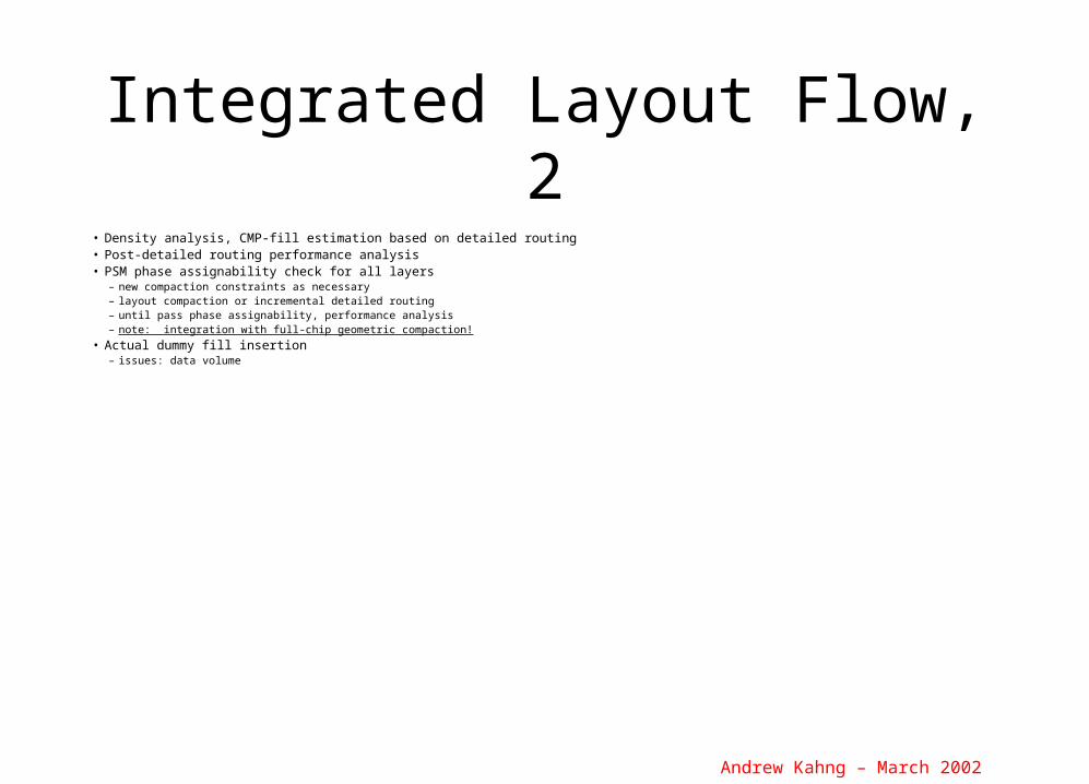
Integrated Layout Flow, 2• Density analysis, CMP-fill estimation based on detailed routing• Post-detailed routing performance analysis• PSM phase assignability check for all layers
– new compaction constraints as necessary– layout compaction or incremental detailed routing– until pass phase assignability, performance analysis– note: integration with full-chip geometric compaction!
• Actual dummy fill insertion– issues: data volume

Andrew Kahng – March 2002
Integrated Layout Flow, 3• Detailed physical verification (geom, conn, perf)• Full-chip OPC insertion
– issues: min-cost OPC that achieves required function– issues: data volumes, metrics, intermediate formats– issues: tools stepping on each other (line extensions in DSM router rules are “zeroth-order OPC”, for example)
• Full-chip printability check• Silicon-level DRC/LVS/performance analysis
Andrew Kahng – March 2002
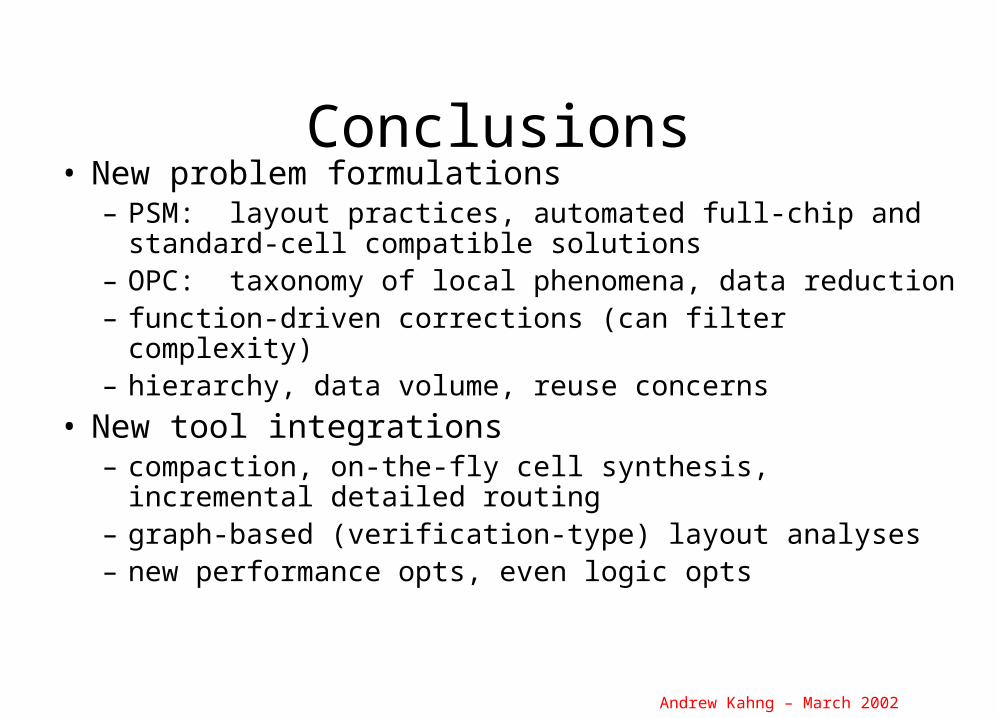
Conclusions• New problem formulations
– PSM: layout practices, automated full-chip and standard-cell compatible solutions
– OPC: taxonomy of local phenomena, data reduction– function-driven corrections (can filter complexity)– hierarchy, data volume, reuse concerns
• New tool integrations– compaction, on-the-fly cell synthesis, incremental detailed
routing– graph-based (verification-type) layout analyses– new performance opts, even logic opts
Andrew Kahng – March 2002
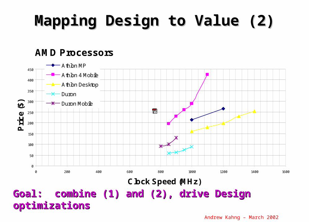
AMD Processors
0
50
100
150
200
250
300
350
400
450
0 200 400 600 800 1000 1200 1400 1600
Clock Speed (MHz)
Pri
ce
($
)
Athlon MP
Athlon 4 Mobile
Athlon Desktop
Duron
Duron Mobile
Mapping Design to Value (2)Mapping Design to Value (2)
Goal: combine (1) and (2), drive Design optimizationsGoal: combine (1) and (2), drive Design optimizations

Andrew Kahng – March 2002
Need for Density Awareness in Layout
• Performance verification flow:
• Filling/slotting geometries affect RC extractionRCX ROM
DelayCalc
Timing/Noise Analysis
-15
VICTIM LAYER TOTAL CAPACITANCE (10 F)Same layer-i neighbors?
Fill layers i-1, i+1? = 3.9 = 2.7
N N 2.43 (1.0) 1.68 (1.0) N Y 3.73 (1.54) 2.58 (1.54) Y N 4.47 (1.84) 3.09 (1.84) Y Y 5.29 (2.18) 3.66 (2.18)
Up to 1% error in extracted capacitanceReliability also affected (e.g. slotting of power stripes)
Andrew Kahng – March 2002
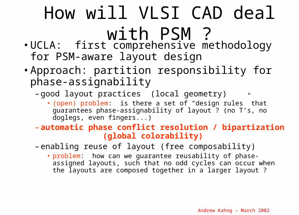
How will VLSI CAD deal with PSM ?• UCLA: first comprehensive methodology for
PSM-aware layout design• Approach: partition responsibility for phase-
assignability – good layout practices (local geometry)
• (open) problem: is there a set of “design rules” that guarantees phase-assignability of layout ? (no T’s, no doglegs, even fingers...)
– automatic phase conflict resolution / bipartization (global colorability)
– enabling reuse of layout (free composability)• problem: how can we guarantee reusability of phase-assigned
layouts, such that no odd cycles can occur when the layouts are composed together in a larger layout ?
Andrew Kahng – March 2002
Background: ITRS Acceleration and System Drivers
ITRS = International Technology Roadmap for Semiconductors, http://public.itrs.net
Andrew Kahng – March 2002
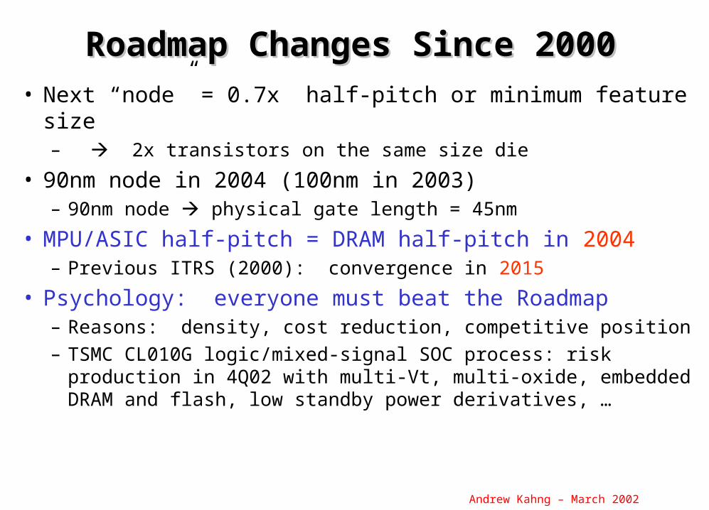
Roadmap Changes Since 2000Roadmap Changes Since 2000
• Next “node” = 0.7x half-pitch or minimum feature size– 2x transistors on the same size die
• 90nm node in 2004 (100nm in 2003)– 90nm node physical gate length = 45nm
• MPU/ASIC half-pitch = DRAM half-pitch in 2004– Previous ITRS (2000): convergence in 2015
• Psychology: everyone must beat the Roadmap– Reasons: density, cost reduction, competitive position– TSMC CL010G logic/mixed-signal SOC process: risk
production in 4Q02 with multi-Vt, multi-oxide, embedded DRAM and flash, low standby power derivatives, …
Andrew Kahng – March 2002
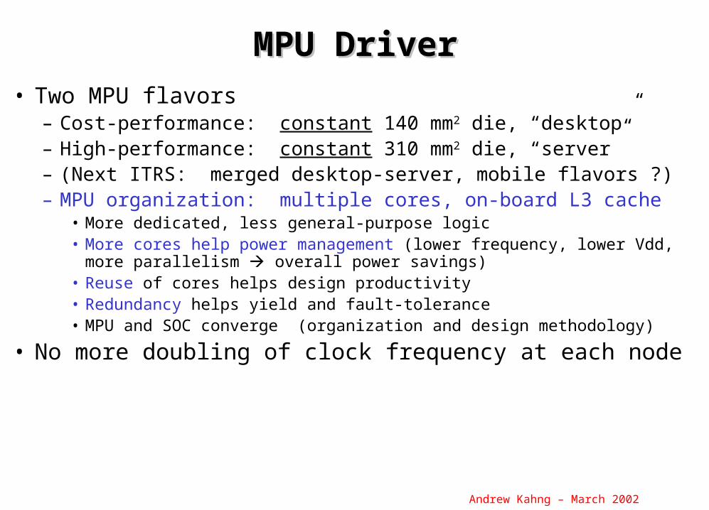
MPU DriverMPU Driver
• Two MPU flavors– Cost-performance: constant 140 mm2 die, “desktop”– High-performance: constant 310 mm2 die, “server”– (Next ITRS: merged desktop-server, mobile flavors ?)– MPU organization: multiple cores, on-board L3 cache
• More dedicated, less general-purpose logic• More cores help power management (lower frequency, lower Vdd,
more parallelism overall power savings)• Reuse of cores helps design productivity• Redundancy helps yield and fault-tolerance• MPU and SOC converge (organization and design methodology)
• No more doubling of clock frequency at each node
Andrew Kahng – March 2002
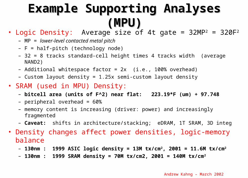
• Logic Density: Average size of 4t gate = 32MP2 = 320F2
– MP = lower-level contacted metal pitch
– F = half-pitch (technology node)
– 32 = 8 tracks standard-cell height times 4 tracks width (average NAND2)
– Additional whitespace factor = 2x (i.e., 100% overhead)
– Custom layout density = 1.25x semi-custom layout density
• SRAM (used in MPU) Density:– bitcell area (units of F^2) near flat: 223.19*F (um) + 97.748
– peripheral overhead = 60%
– memory content is increasing (driver: power) and increasingly fragmented
– Caveat: shifts in architecture/stacking; eDRAM, 1T SRAM, 3D integ
• Density changes affect power densities, logic-memory balance– 130nm : 1999 ASIC logic density = 13M tx/cm2, 2001 = 11.6M tx/cm2
– 130nm : 1999 SRAM density = 70M tx/cm2, 2001 = 140M tx/cm2
Example Supporting Analyses (MPU)Example Supporting Analyses (MPU)
Andrew Kahng – March 2002
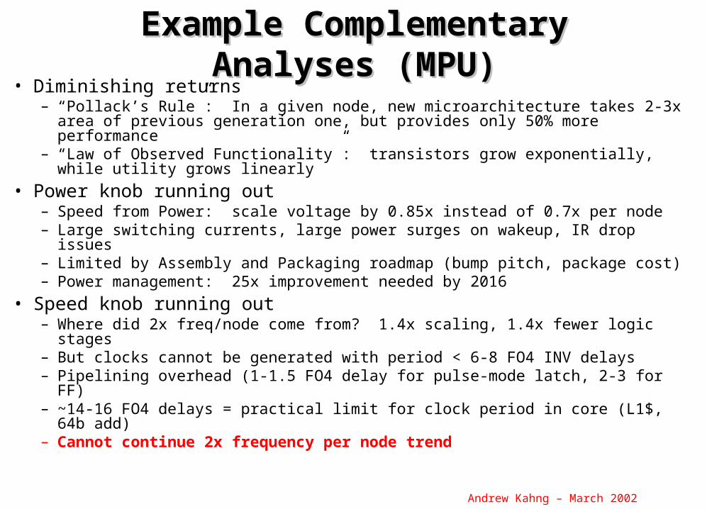
• Diminishing returns– “Pollack’s Rule”: In a given node, new microarchitecture takes 2-3x area
of previous generation one, but provides only 50% more performance– “Law of Observed Functionality”: transistors grow exponentially, while
utility grows linearly
• Power knob running out– Speed from Power: scale voltage by 0.85x instead of 0.7x per node– Large switching currents, large power surges on wakeup, IR drop issues– Limited by Assembly and Packaging roadmap (bump pitch, package cost)– Power management: 25x improvement needed by 2016
• Speed knob running out– Where did 2x freq/node come from? 1.4x scaling, 1.4x fewer logic stages– But clocks cannot be generated with period < 6-8 FO4 INV delays– Pipelining overhead (1-1.5 FO4 delay for pulse-mode latch, 2-3 for FF)– ~14-16 FO4 delays = practical limit for clock period in core (L1$, 64b add)– Cannot continue 2x frequency per node trend
Example Complementary Analyses Example Complementary Analyses (MPU)(MPU)

Andrew Kahng – March 2002
FO4 INV Delays Per Clock Period
• FO4 INV = inverter driving 4 identical inverters (no interconnect)• Half of freq improvement has been from reduced logic stages

Andrew Kahng – March 2002
SOC Low-Power Driver Model (STRJ)SOC Low-Power Driver Model (STRJ)
• SOC-LP “PDA” system– Composition: CPU cores, embedded cores, SRAM/eDRAM– Requirements: IO bandwidth, computational power, GOPS/mW, die size
• Drives PIDS/FEP LP device roadmap, Design power management challenges, Design productivity challenges
Year of Products 2001 2004 2007 2010 2013 2016Process Technology (nm) 130 90 65 45 32 22Operation Voltage (V) 1.2 1 0.8 0.6 0.5 0.4Clock Frequency (MHz) 150 300 450 600 900 1200Application Still Image Processing Real Time Video Code Real Time Interpretation (MAX performance required) (MPEG4/CIF)Application Web Browser TV Telephone (1:1) TV Telephone (>3:1)(Others) Electric Mailer Voice Recognition (Input) Voice Recognition (Operation)
Scheduler Authentication (Crypto Engine)Processing Performance (GOPS) 0.3 2 15 103 720 5042Communication Speed (Kbps) 64 384 2304 13824 82944 497664Power Consumption (mW/MOPS) 0.3 0.2 0.1 0.03 0.01 0.006Peak Power Consumption (W) 0.1 0.3 1.1 2.9 10.0 31.4(Requirement) 0.1 0.1 0.1 0.1 0.1Standby power consumption (mW) 2.1 2.1 2.1 2.1 2.1 2.1Addressable System Memory (Gb) 0.1 1 10 100 1000 10000

Andrew Kahng – March 2002
Key SOC-LP ChallengesKey SOC-LP Challenges• Power management challenge
– Above and beyond low-power process innovation– Hits SOC before MPU– Need slower, less leaky devices: low-power lags high-perf by 2 years– Low Operating Power and Low Standby Power flavors design tools
handle multi (Vt,Tox,Vdd)
• Design productivity challenge– Logic increases 4x per node; die size increases 20% per node
Year 2001 2004 2007 2010 2013 2016
½ Pitch 130 90 65 45 32 22
Logic Mtx per designer-year
1.2 2.6 5.9 13.5 37.4 117.3
Dynamic power reduction (X)
0 1.5 2.5 4 7 20
Standby power reduction (X)
2 6 15 39 150 800

Andrew Kahng – March 2002
Parameter Type 99 00 01 02 03 04 05 06 07 10 13 16
Tox (nm) MPU 3.00 2.30 2.20 2.20 2.00 1.80 1.70 1.70 1.30 1.10 1.00 0.90
LOP 3.20 3.00 2.2 2.0 1.8 1.6 1.4 1.3 1.2 1.0 0.9 0.8
LSTP 3.20 3.00 2.6 2.4 2.2 2.0 1.8 1.6 1.4 1.1 1.0 0.9
Vdd MPU 1.5 1.3 1.2 1.1 1.0 1.0 0.9 0.9 0.7 0.6 0.5 0.4
LOP 1.3 1.2 1.2 1.2 1.1 1.1 1.0 1.0 0.9 0.8 0.7 0.6
LSTP 1.3 1.2 1.2 1.2 1.2 1.2 1.2 1.2 1.1 1.0 0.9 0.9
Vth (V) MPU 0.21 0.19 0.19 0.15 0.13 0.12 0.09 0.06 0.05 0.021 0.003 0.003
LOP 0.34 0.34 0.34 0.35 0.36 0.32 0.33 0.34 0.29 0.29 0.25 0.22
LSTP 0.51 0.51 0.51 0.52 0.53 0.53 0.54 0.55 0.52 0.49 0.45 0.45
Ion (uA/um) MPU 1041 1022 926 959 967 954 924 960 1091 1250 1492 1507
LOP 636 591 600 600 600 600 600 600 700 700 800 900
LSTP 300 300 300 300 400 400 400 400 500 500 600 800
CV/I (ps) MPU 2.00 1.64 1.63 1.34 1.16 0.99 0.86 0.79 0.66 0.39 0.23 0.16
LOP 3.50 2.87 2.55 2.45 2.02 1.84 1.58 1.41 1.14 0.85 0.56 0.35
LSTP 4.21 3.46 4.61 4.41 2.96 2.68 2.51 2.32 1.81 1.43 0.91 0.57
Ioff (uA/um) MPU 0.00 0.01 0.01 0.03 0.07 0.10 0.30 0.70 1.00 3 7 10
LOP 1e-4 1e-4 1e-4 1e-4 1e-4 3e-4 3e-4 3e-4 7e-4 1e-3 3e-3 1e-2
LSTP 1e-6 1e-6 1e-6 1e-6 1e-6 1e-6 1-6 1e-6 1-6 3e-6 7e-6 1e-5
Gate L (nm) MPU 100 70 65 53 45 37 32 30 25 18 13 9
L(*)P 110 100 90 80 65 53 45 37 32 22 16 11
LP Device RoadmapLP Device Roadmap
Andrew Kahng – March 2002
• Today, the digital part of circuits is most critical for performance and is dominating chip area
• But in many new IC-products the mixed-signal part becomes important for performance and cost
• This shift requires definition of the “analog boundary conditions” in the design part of the ITRS
• Goal: define criteria and needs for future analog/RF circuit performance, and compare to device parameters:
• Choose critical, important analog/RF circuits
• Identify circuit performance needs
• and related device parameter needs
Mixed-Signal Driver (Europe)Mixed-Signal Driver (Europe)

Andrew Kahng – March 2002
OutlineOutline
• 1. Background: ITRS and system drivers• 2. Design Roadmap• 3. Sharing red bricks• 4. Example: Design-manufacturing handoff• 5. Conclusion
Andrew Kahng – March 2002
OutlineOutline
• 1. Background: ITRS and system drivers• 2. Design Roadmap• 3. Sharing red bricks• 4. Example: Design-manufacturing handoff• 5. Conclusion
Andrew Kahng – March 2002
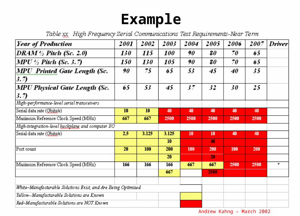
Example

Andrew Kahng – March 2002
““Living ITRS” FrameworkLiving ITRS” Framework
Andrew Kahng – March 2002
OutlineOutline
• 1. Background: ITRS and system drivers• 2. Design Roadmap• 3. Sharing red bricks• 4. Example: Design-manufacturing handoff• 5. Conclusion

Andrew Kahng – March 2002
2001 Big Picture2001 Big Picture• Message from the Design ITWG: Cost of Design
threatens continuation of the semiconductor roadmap– Design cost model– Challenges are now Crises
• Must strengthen bridge between semiconductors and applications, software, architectures– Frequency and bits are not the same as efficiency and utility– New System Drivers chapter, with productivity and power foci
• Must strengthen bridges between ITRS technologies– Are there synergies that “share red bricks” more cost-
effectively than independent technological advances?– “Manufacturing Integration” cross-cutting challenge– “Living ITRS” framework to promote consistency validation