angle-dependent optical perfect absorption and enhanced
TRANSCRIPT

Angle-dependent optical perfect absorption and enhanced photoluminescence in excitonic thin films BYUNG HOON WOO,1,2 IN CHEOL SEO,1,2 EUNSONGYI LEE,1 SOO-CHAN AN,1 HOON YEUB JEONG,1 AND YOUNG CHUL JUN1,* 1School of Materials Science and Engineering, Ulsan National Institute of Science and Technology (UNIST), Ulsan 44919, South Korea 2These authors contributed equally to the paper *[email protected]
Abstract: We experimentally demonstrate perfect absorption of incident light in an ultrathin, planar organic layer, together with large photoluminescence (PL) enhancement. We find that diverse features appear in the absorption spectra of J-aggregate excitonic films, depending on the incident light angle and the phase controller thickness. We achieve strong absorption even away from the excitonic absorption pole. We explain the angle-dependent perfect absorption by comparing radiative and nonradiative damping rates for different incident angles. Moreover, we achieve large PL enhancement at strong light absorption conditions. This demonstrates that the absorbed light energy in excitonic perfect absorbers can be retrieved, unlike other perfect absorbers based on metal nanostructures where the absorbed energy is mainly dissipated as heat due to ohmic losses. Excitonic perfect absorbers can be useful for energy conversion devices or fluorescence-based optical devices. © 2017 Optical Society of America
OCIS codes: (300.1030) Absorption; (310.6188) Spectral properties; (310.6845) Thin film devices and applications; (160.4890) Organic materials; (160.2540) Fluorescent and luminescent materials.
References and links 1. N. I. Landy, S. Sajuyigbe, J. J. Mock, D. R. Smith, and W. J. Padilla, “Perfect metamaterial absorber,” Phys.
Rev. Lett. 100(20), 207402 (2008). 2. N. Liu, M. Mesch, T. Weiss, M. Hentschel, and H. Giessen, “Infrared perfect absorber and its application as
plasmonic sensor,” Nano Lett. 10(7), 2342–2348 (2010). 3. R. Alaee, M. Farhat, C. Rockstuhl, and F. Lederer, “A perfect absorber made of a graphene micro-ribbon
metamaterial,” Opt. Express 20(27), 28017–28024 (2012). 4. Y. Cui, Y. He, Y. Jin, F. Ding, L. Yang, Y. Ye, S. Zhong, Y. Lin, and S. He, “Plasmonic and metamaterial
structures as electromagnetic absorbers,” Laser Photonics Rev. 8(4), 495–520 (2014). 5. J. R. Piper and S. Fan, “Total absorption in a graphene monolayer in the optical regime by critical coupling with
a photonic crystal guided resonance,” ACS Photonics 1(4), 347–353 (2014). 6. Y. Ra’di, C. R. Simovski, and S. A. Tretyakov, “Thin perfect absorbers for electromagnetic waves: theory,
design, and realizations,” Phys. Rev. Appl. 3(3), 037001 (2015). 7. S. M. Bahauddin, H. Robatjazi, and I. Thomann, “Broadband absorption engineering to enhance light absorption
in monolayer MoS2,” ACS Photonics 3(5), 853–862 (2016). 8. M. A. Kats, D. Sharma, Z. Yang, and F. Capasso, “Ultra-thin perfect absorber employing a tunable phase change
material,” Appl. Phys. Lett. 101(22), 221101 (2012). 9. M. A. Kats, R. Blanchard, P. Genevet, and F. Capasso, “Nanometre optical coatings based on strong interference
effects in highly absorbing media,” Nat. Mater. 12(1), 20–24 (2013). 10. J. Park, J.-H. Kang, A. P. Vasudev, D. T. Schoen, H. Kim, E. Hasman, and M. L. Brongersma, “Omnidirectional
near-unity absorption in an ultrathin planar semiconductor layer on a metal substrate,” ACS Photonics 1(9), 812–821 (2014).
11. T. S. Luk, S. Campione, I. Kim, S. Feng, Y. C. Jun, S. Liu, J. B. Wright, I. Brener, P. B. Catrysse, S. Fan, and M. B. Sinclair, “Directional perfect absorption using deep subwavelength low permittivity films,” Phys. Rev. B 90(8), 085411 (2014).
12. M. A. Badsha, Y. C. Jun, and C. K. Hwangbo, “Admittance matching analysis of perfect absorption in unpattern thin films,” Opt. Commun. 332, 206–213 (2014).
13. J. Yoon, M. Zhou, M. A. Badsha, T. Y. Kim, Y. C. Jun, and C. K. Hwangbo, “Broadband epsilon-near-zero perfect absorption in the near-infrared,” Sci. Rep. 5, 12788 (2015).
Vol. 25, No. 23 | 13 Nov 2017 | OPTICS EXPRESS 28619
#305930 https://doi.org/10.1364/OE.25.028619 Journal © 2017 Received 29 Aug 2017; revised 31 Oct 2017; accepted 31 Oct 2017; published 3 Nov 2017

14. T. Y. Kim, M. A. Badsha, J. Yoon, S. Y. Lee, Y. C. Jun, and C. K. Hwangbo, “General strategy for broadband coherent perfect absorption and multi-wavelength all-optical switching based on epsilon-near-zero multilayer films,” Sci. Rep. 6, 22941 (2016).
15. J.-B. You, W.-J. Lee, D. Won, and K. Yu, “Multiband perfect absorbers using metal-dielectric films with optically dense medium for angle and polarization insensitive operation,” Opt. Express 22(7), 8339–8348 (2014).
16. Z. Li, S. Butun, and K. Aydin, “Large-area, lithography-free super absorbers and color filters at visible frequencies using ultrathin metallic films,” ACS Photonics 2(2), 183–188 (2015).
17. S. S. Mirshafieyan, T. S. Luk, and J. Guo, “Zeroth order Fabry-Perot resonance enabled ultra-thin perfect light absorber using percolation aluminum and silicon nanofilms,” Opt. Mater. Express 6(4), 1032–1042 (2016).
18. G. Kenanakis, Ch. P. Mavidis, E. Vasilaki, N. Katsarakis, M. Kafesaki, E. N. Economou, and C. M. Soukoulis, “Perfect absorbers based on metal–insulator–metal structures in the visible region: a simple approach for practical applications,” Appl. Phys., A Mater. Sci. Process. 123(1), 77 (2017).
19. M. S. Bradley, J. R. Tischler, and V. Bulović, “Layer-by-Layer J-aggregate thin films with a peak absorption constant of 106 cm−1,” Adv. Mater. 17(15), 1881–1886 (2005).
20. L. Gu, J. Livenere, G. Zhu, E. E. Narimanov, and M. A. Noginov, “Quest for organic plasmonics,” Appl. Phys. Lett. 103(2), 021104 (2013).
21. M. J. Gentile, S. Núñez-Sánchez, and W. L. Barnes, “Optical field-enhancement and subwavelength field-confinement using excitonic nanostructures,” Nano Lett. 14(5), 2339–2344 (2014).
22. A. Cacciola, C. Triolo, O. D. Stefano, A. Genco, M. Mazzeo, R. Saija, S. Patanè, and S. Savasta, “Subdiffraction light concentration by J-aggregate nanostructures,” ACS Photonics 2(7), 971–979 (2015).
23. B. H. Woo, I. C. Seo, E. Lee, S. Y. Kim, T. Y. Kim, S. C. Lim, H. Y. Jeong, C. K. Hwangbo, and Y. C. Jun, “Dispersion control of excitonic thin films for tailored super-absorption in the visible region,” ACS Photonics 4(5), 1138–1145 (2017).
24. S. K. Saikin, A. Eisfeld, S. Valleau, and A. Aspuru-Guzik, “Photonics meets excitonics: natural and artificial molecular aggregates,” Nanophotonics 2(1), 21–38 (2013).
25. Few Chemicals, “special chemicals,” http://www.few.de/1/special-chemicals/functional-dyes/water-soluble-cyanine-dyes/500-699-nm/ (CAS #18462–64–1).
26. R. T. Phillips, “A numerical method for determining the complex refractive index from reflectance and transmittance of supported thin films,” J. Phys. D Appl. Phys. 16(4), 489–497 (1983).
27. J. R. Tischler, M. S. Bradley, and V. Bulović, “Critically coupled resonators in vertical geometry using a planar mirror and a 5 nm thick absorbing film,” Opt. Lett. 31(13), 2045–2047 (2006).
28. B. Ding, M. Qiu, and R. J. Blaikie, “Manipulating light absorption in dye-doped dielectric films on reflecting surfaces,” Opt. Express 22(21), 25965–25975 (2014).
29. B. E. A. Saleh and M. C. Teich, Fundamentals of Photonics (Wiley, 2007) Chap. 7. 30. S. Fan, W. Suh, and J. D. Joannopoulos, “Temporal coupled-mode theory for the Fano resonance in optical
resonators,” J. Opt. Soc. Am. A 20(3), 569–572 (2003). 31. S. Collin, “Nanostructure arrays in free-space: optical properties and applications,” Rep. Prog. Phys. 77(12),
126402 (2014). 32. L. Zhu, F. Liu, H. Lin, J. Hu, Z. Yu, X. Wang, and S. Fan, “Angle-selective perfect absorption with two-
dimensional materials,” Light Sci. Appl. 5, e16052 (2016). 33. D. Liu and Q. Li, “Sub-nanometer planar solar absorber,” Nano Energy 34, 172–180 (2017). 34. J. D. Jackson, Classical Electrodynamics (Wiley, 1999) Chap. 6. 35. J. Xiao, M. Zhao, Y. Wang, and X. Zhang, “Excitons in atomically thin 2D semiconductors and their
applications,” Nanophotonics 6(6), 160 (2017). 36. J. Huang, Y. Yuan, Y. Shao, and Y. Yan, “Understanding the physical properties of hybrid perovskites for
photovoltaic applications,” Nat. Rev. Mater. 2, 17042 (2017).
1. Introduction Ultrathin perfect absorbers have been actively studied recently [1–18]. Resonant metal nanostructures have been often used together with a back reflection mirror to suppress transmission and induce the destructive interference of reflected light. These perfect absorbers could be useful for certain applications, such as optical filters and sensors. However, in these structures, light is strongly absorbed in metal layers and is eventually dissipated as heat due to ohmic losses. Therefore, these perfect absorbers have the limited use in applications such as efficient photodetectors or energy conversion devices.
Some organic molecules such as J-aggregates have large oscillator strength and can have very sharp excitonic absorption lines, which could lead to an optically metallic response (Re[ε] < 0) in the visible spectral range [19–23]. J-aggregates also support efficient exciton transfer across aggregated molecules, which could be useful for light detection or energy harvesting [24]. Therefore, these excitonic materials hold good promise for optical devices based on perfect absorbers.
Vol. 25, No. 23 | 13 Nov 2017 | OPTICS EXPRESS 28620

In this paper, we demonstrate perfect light absorption in a planar organic layer, spin-coated over a large area, together with strong photoluminescence (PL) enhancement. Ultrathin J-aggregate excitonic films (~35 nm in thickness) are spin-coated on a substrate that consists of an oxide phase controller and a silver back mirror as shown in Fig. 1. Depending on the incident light angle and the phase controller thickness, we observe diverse features appear in the absorption spectra. We can achieve perfect absorption in various conditions (in both metallic and dielectric spectral regions of the excitonic film) and get strong absorption even away from the excitonic absorption pole. We explain this diverse absorption behavior by analyzing critical coupling conditions in the excitonic films. By comparing the radiative and nonradiative (i.e. internal) damping rates for different incident angles, we explain the angle-dependent absorption features. Moreover, we find that incident light is strongly absorbed in the organic layer and this leads to the large enhancement of PL too. We verify that the experimentally observed PL intensity follows the absorption spectra of the excitonic films. We also achieve large PL enhancement at strong light absorption conditions.
These excitonic perfect absorbers can be fabricated easily over a large area without lithographic patterning, and they may find applications in novel optoelectronic devices or energy conversion devices. Strong PL enhancement could be also very useful for fluorescence-based optical devices (such as fluorescence sensors). We believe that our experimental and theoretical investigations provide useful guidelines for novel devices based on excitonic perfect absorbers.
Fig. 1. (a) Dielectric constants of the excitonic film. The imaginary part of dielectric constants has a strong and sharp pole near 590 nm. The optically metallic region (Re[ε] < 0) appears right below the pole. (b) Schematic of the sample ([Excitonic film/SiO2/Ag]) and the measurement condition (oblique incidence of light). (c) Picture of the three samples (tox = 47 nm, 96 nm, 150 nm). Color looks slightly different for three samples with different oxide thicknesses.
2. Sample preparation and characterization In our experiment, a water-soluble cyanine dye was used (TDBC: 5,6-dichloro-2-[[5,6-dichloro-1-ethyl-3-(4-sulphobutyl)-benzimidazol-2-ylidene]-propenyl]-1-ethyl-3-(4-sulpho butyl)-benzi- midazoliumhydroxide, sodium salt, inner salt) [25]. It was mixed in a poly vinyl alcohol (PVA) matrix and spin-coated on a substrate. TDBC and PVA powders were
Vol. 25, No. 23 | 13 Nov 2017 | OPTICS EXPRESS 28621

dissolved in distilled water separately in 2.5 wt% and 2 wt%, respectively. And then two solutions were mixed together in a 3:1 volume ratio and agitated using a vortex machine. Finally, a TDBC/PVA film was spin-coated on a substrate with the spin speed of 4000 rpm for 60s. The film thickness was measured using AFM (DI-3100, Veeco). We first made several scratches on the organic film and scanned the surface over scratches. By taking an average of the measured values, we determined the final film thickness (~35 nm).
Figure 1(a) shows the dielectric constants of the excitonic film used in our measurement. These dielectric constants were extracted from the measured reflection-transmission spectra by fitting them to the Fresnel’s equations [23, 26]. The imaginary part of the dielectric constants (Im[ε]) has a sharp pole near 590 nm, and we have the optically metallic region (Re[ε] < 0) right below this excitonic pole wavelength. Away from this metallic region (either in the shorter or longer wavelength region), we again have a normal dielectric response (Re[ε] > 0). This can be easily understood from the Kramers-Kronig relation; when there is a large absorption peak at a certain wavelength, it also becomes highly dispersive. The real part of the dielectric constant value fluctuates severely, and it can become negative. Therefore, spin-coated organic films can also show optically metallic behavior in the visible region.
The imaginary part of the dielectric constants (Im[ε]) indicates the optical loss, and it has a maximum value around 590 nm and decreases rapidly away from this wavelength. The position of this excitonic pole can be considered as an intrinsic molecular property. Organic dye molecules have been used for light absorbers widely [19, 27, 28], but the absorption enhancement was mainly limited to this intrinsic pole region. However, we show that, by combining with planar perfect absorber structures, the actual absorption spectra of excitonic films can be altered in a significant way, depending on the angle of incident light. We can achieve perfect absorption in both metallic and dielectric spectral regions of excitonic films and can obtain strong light absorption even away from the excitonic pole.
Figure 1(b) shows our sample structure ([Excitonic film/SiO2/Ag]). A thick silver film (~200 nm) was first deposited on a quartz substrate (1” x 1” in size) by e-beam evaporator, and then a silicon dioxide (SiO2) layer was deposited on top by sputtering. The silver back mirror suppresses light transmission, and the oxide layer works as a phase controller. We vary the oxide layer thickness and the angle of incident light, and control light absorption strength in the excitonic layer. We prepared three samples with different oxide thicknesses (tox = 47 nm, 96 nm, 150 nm), and Fig. 1(c) shows the picture of these samples. Color looks slightly different for these three samples.
3. Results and discussion Figures 2 and 3 summarize the measured and calculated absorption spectra for three excitonic samples. Figures 2(a)-2(c) and 3(a)-3(c) show the measured absorption spectra for p-polarized [Fig. 2] and s-polarized [Fig. 3] incident light. Incident angles are varied from 20° to 70°. We compare the absorption spectra in three samples with different oxide thicknesses. In overall, we find diverse features appear in the absorption spectra.
For example, in Fig. 2(a) (tox = 47 nm, p-polarization), strong absorption appears at small incidence angles around 530 nm, and the absorption intensity gradually decreases with increasing angles. In Fig. 2(b) (tox = 96 nm, p-polarization), near-perfect absorption (A ~98.5%) is achieved around 560 nm over a large range of incidence angles. In both cases, another strong absorption peak appears on the longer wavelength side at a very large incident angle (~70°). In Fig. 2(c) (tox = 150 nm, p-polarization), a large absorption peak appears around 570 nm with increasing angles. The angle dependence is indicated as dotted arrows in the figure.
For s-polarization, we observe different behavior. In Fig. 3(a) (tox = 47 nm, s-polarization), the absorption peak around 530 nm decreases with increasing angles, but another absorption peak appears on the shorter wavelength side. And also strong absorption appears in the very long wavelength region (> 700 nm) at the same time. Note that this behavior is quite different
Vol. 25, No. 23 | 13 Nov 2017 | OPTICS EXPRESS 28622

from that from the p-polarization case in Fig. 2(a). In Fig. 3(b) (tox = 96 nm, s-polarization), near-perfect absorption appears as in Fig. 2(b), but this time the peak position gradually blueshifts with increasing angles. Therefore, the perfect absorption wavelength spans from 560 nm to 500 nm depending on angles. In Fig. 3(c) (tox = 150 nm, s-polarization), the absorption peak appears again around 570 nm with increasing angles as in Fig. 2(c), but it reaches the maximum at the angle of 60° and the absorption decreases back. In these cases, the angle dependence is again indicated as dotted arrows. Therefore, we can obtain highly diverse absorption spectra with different phase controller layer thicknesses and incident angles.
To investigate the angle and oxide thickness dependence further, we also performed transfer matrix method (TMM) calculations [29], and obtained the absorption spectra colormaps as a function of wavelength and incidence angle; Figs. 2(d)-2(f) for p-polarization and Figs. 3(d)-3(f) for s-polarization. In these calculations, we used the extracted dielectric constants of the excitonic film, given in Fig. 1(a). We find that the calculated absorption spectra agree well with experimentally measured ones in overall. Although peak absorption values are slightly different from the measured ones in some cases, this could be possibly due to non-idealities in our large-area planar samples (such as surface roughness, film thickness variation, etc). In measurements, the range of incident angles was limited to 20° ~70°, but in TMM calculations, we considered the full range of angles (0 ° ~90°) to obtain the complete picture of absorption behavior.
Fig. 2. p-polarized absorption spectra for three samples. (a)-(c) measured absorption spectra and (d)-(f) calculated absorption spectra maps. Three samples show different angular dependence, as indicated by dotted arrows. For tox = 96 nm, near-perfect absorption is experimentally achieved (A ~98.5%) over a broad range of incident angle.
Vol. 25, No. 23 | 13 Nov 2017 | OPTICS EXPRESS 28623

Fig. 3. s-polarized absorption spectra for three samples. (a)-(c) measured absorption spectra and (d)-(f) calculated absorption spectra maps. For tox = 96nm, the near-perfect absorption peak blueshifts with increasing angles. Three samples show different angular dependence, as indicated by dotted arrows.
We note that perfect absorption and strong absorption can occur in various conditions, even away from the excitonic pole wavelength (~590 nm). This means that absorption spectrum control in excitonic films is possible to a large degree, using different phase controller thicknesses and incident angles. This, in turn, provides us more freedom to design our optical absorbers with a single absorbing material.
To understand this diverse behavior in the absorption spectra, we evaluated critical coupling conditions in the excitonic film by comparing the radiative damping rate γrad and the internal (i.e. nonradiative) damping rate γnonrad for different incident angles. The internal damping rate results from material losses, while the radiative damping rate is determined by the light leakage rate from the resonant structure. From the temporal coupled mode theory [30, 31], the absorption spectrum is given by
2 2
0
4( ) ,
( ) ( )rad nonrad
rad nonrad
Aγ γω
ω ω γ γ=
− + + (1)
where ω0 is the resonant frequency. At the resonant frequency ω0, we have the maximum absorption
2
4.
( )rad nonrad
mrad nonrad
Aγ γ
γ γ=
+ (2)
Therefore, when γrad = γnonrad (i.e. critical coupling), we achieve perfect absorption Am = 1. We used the absorption spectra from numerical simulations to extract out radiative and
nonradiative damping rates. An absorption spectrum was first fitted to a Lorentzian curve to determine the resonance linewidth (2γtotal). Then, by combining Eq. (1) with the total damping rate (γtotal = γrad + γnonrad), we obtained two numerical values for damping rates. Because Eq. (1) is symmetric regarding to radiative and nonradiative rates, we still need to decide which one is radiative (or nonradiative). To this end, we performed numerical simulations again by
Vol. 25, No. 23 | 13 Nov 2017 | OPTICS EXPRESS 28624

intentionally reducing the optical loss (Im[ε]). We found that one of two damping rates gradually decreases with reduced losses, while the other remains almost the same or increases slightly. Therefore, we could identify the former one is a nonradiative damping rate γnonrad, and the later one is a radiative damping rate γrad.
Fig. 4. Analysis of critical coupling conditions. Radiative and nonradiative damping rates are extracted from the calculated data for two cases. (a) tox = 47 nm (s-polarization): two damping rates crosses around 86°, where perfect absorption occurs. (b) tox = 96 nm (p-polarization): two damping rates are very close and we obtain perfect absorption over a broad range of angles (near normal incidence). The difference between them becomes larger when the incident angle increases.
We first consider perfect absorption for s-polarized light in the 47 nm oxide sample. The dotted circle in Fig. 3(d) indicates the perfect absorption condition in the dielectric, low-loss spectral region of the excitonic film (i.e. small Im[ε]). This perfect absorption occurs at very large incident angle (~86°). As described above, we extracted radiative and nonradiative damping rates for each incident angle, as shown in Fig. 4(a). We find that two damping rates have a different angular dependence and cross each other around the angle of 86°. That is, the critical coupling condition is satisfied at this angle. Because two rates become the same at this point, we can achieve perfect absorption even in the ultra-thin, low-loss film. We note that similar perfect absorption at grazing angles has been also considered for 2-dimensional materials such as graphene [32] and MoS2 [33].
We also consider broad-angle perfect absorption for p-polarized light in the 96 nm oxide sample (the dotted region in Fig. 2(b)). This perfect absorption occurs near normal incidence of light, which is quite different from the previous one. It is located in the metallic spectral region of the excitonic film. Again, we extracted radiative and nonradiative damping rates for each incident angle, as shown in Fig. 4(b). To consider the effect of the weak absorption shoulder in the spectra, we used two Lorentzian terms for linewidth fitting. This time, we find that two damping rates are very close over a broad range of angle, and they are separated at larger angles (> 30°). Therefore, we can achieve broad-angle perfect absorption near normal incidence. In the excitonic film, we can control the radiative and nonradiative damping rates to a very large degree, and thus we obtain diverse features in the absorption spectra. We can achieve critical coupling in either metallic or dielectric spectral region.
We also obtained the absorbed power profile using numerical simulations to see in which layer light is actually absorbed. The absorbed power per unit volume ( absP ) can be obtained
from the divergence of the Poynting vector [34], and we get the following relation:
2
0
1( ) Im[ ( )].
2absP Eω ω ε ε ω= (3)
Vol. 25, No. 23 | 13 Nov 2017 | OPTICS EXPRESS 28625

From the finite-difference time domain (FDTD) simulations, we obtained the absorption power profile. We verified that most of incident light is indeed absorbed in the excitonic layer. In Fig. 5, the absorbed power density in each layer is indicated as color. About 96.74% of incident light power is absorbed in the excitonic layer. It confirms that light is strongly absorbed in the excitonic film.
Fig. 5. Absorption power profile obtained from the FDTD simulation for 1 W of incident light power. The absorption per unit volume (
absP ) is plotted for tox = 96 nm at 566nm (normal
incidence of light). The excitonic layer has strong absorption, as indicated by red color. We find that about 96.74% of total incident light power is absorbed in the excitonic film.
In excitonic materials, the absorbed light energy can be extracted out efficiently. However, in more conventional perfect absorbers made of ‘metal’ nanostructures, the absorbed energy is purely lost due to metal ohmic losses. We may be able to retrieve some of the absorbed energy from metals (e.g. via hot carrier generation), but it is still a very low efficiency process. In our excitonic absorbers, we experimentally verify that the photoluminescence (PL) intensity indeed follows absorption spectra, and we can achieve large PL enhancement at strong light absorption conditions. It is well known that TDBC has bright PL emission and its peak position is very close to the excitonic absorption pole (~590 nm). We measured the PL spectra of our excitonic films, and compared them with the absorption spectra given in Figs. 2 and 3. We gradually scanned the pump light wavelength and observed how the PL spectrum changes to investigate the effect of light absorption on the PL intensity.
Figure 6(a) shows the absorption spectra for the 150 nm oxide sample for the p-polarization of incident light. A strong absorption peak gradually grows up with increasing angles around 570 nm, as indicated by a dotted arrow. We consider PL intensities at two incident angles 15° and 60° in Fig. 6(b), and compare them with the absorption spectra. In PL measurements, the collection of luminescence was done within the emission cone of 25.36°. Figures 6(c) and 6(d) show the PL spectra for the incident angles of 15° and 60° for different pumping wavelengths. At a small incident angle (15°), PL remains weak for almost all pumping wavelengths. However, at a much larger incident angle (60°), the PL intensity increases rapidly with pumping wavelengths and PL becomes very strong.
The integrated PL power is summarized in Fig. 6(b). Two angles 15° and 60° show a stark difference in behavior, and this agrees very well with the absorption spectra in Fig. 6(a); the absorption strength increases rapidly with increasing angles. We also notice that two lines in Fig. 6(b) have a crossing around 500 nm. Again, this can be understood from the absorption
Vol. 25, No. 23 | 13 Nov 2017 | OPTICS EXPRESS 28626
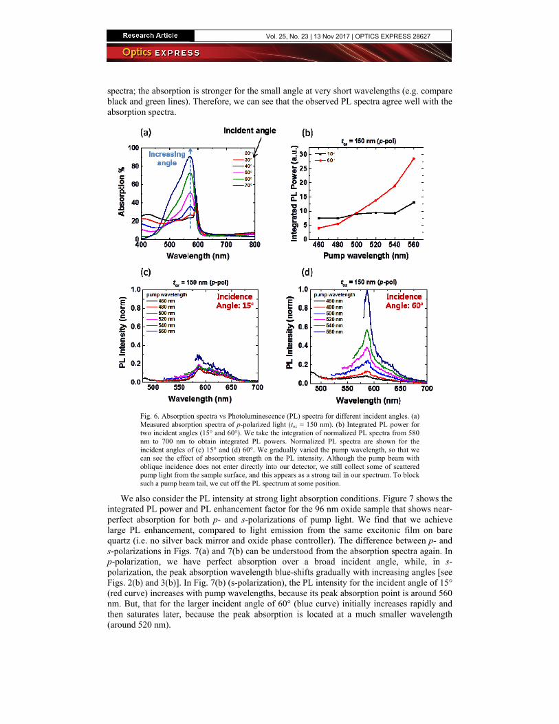
spectra; the absorption is stronger for the small angle at very short wavelengths (e.g. compare black and green lines). Therefore, we can see that the observed PL spectra agree well with the absorption spectra.
Fig. 6. Absorption spectra vs Photoluminescence (PL) spectra for different incident angles. (a) Measured absorption spectra of p-polarized light (tox = 150 nm). (b) Integrated PL power for two incident angles (15° and 60°). We take the integration of normalized PL spectra from 580 nm to 700 nm to obtain integrated PL powers. Normalized PL spectra are shown for the incident angles of (c) 15° and (d) 60°. We gradually varied the pump wavelength, so that we can see the effect of absorption strength on the PL intensity. Although the pump beam with oblique incidence does not enter directly into our detector, we still collect some of scattered pump light from the sample surface, and this appears as a strong tail in our spectrum. To block such a pump beam tail, we cut off the PL spectrum at some position.
We also consider the PL intensity at strong light absorption conditions. Figure 7 shows the integrated PL power and PL enhancement factor for the 96 nm oxide sample that shows near-perfect absorption for both p- and s-polarizations of pump light. We find that we achieve large PL enhancement, compared to light emission from the same excitonic film on bare quartz (i.e. no silver back mirror and oxide phase controller). The difference between p- and s-polarizations in Figs. 7(a) and 7(b) can be understood from the absorption spectra again. In p-polarization, we have perfect absorption over a broad incident angle, while, in s-polarization, the peak absorption wavelength blue-shifts gradually with increasing angles [see Figs. 2(b) and 3(b)]. In Fig. 7(b) (s-polarization), the PL intensity for the incident angle of 15° (red curve) increases with pump wavelengths, because its peak absorption point is around 560 nm. But, that for the larger incident angle of 60° (blue curve) initially increases rapidly and then saturates later, because the peak absorption is located at a much smaller wavelength (around 520 nm).
Vol. 25, No. 23 | 13 Nov 2017 | OPTICS EXPRESS 28627

Fig. 7. Integrated PL power for tox = 96nm. We compare two incident angles: red line (15°) and blue line (60°). (a) p-polarization and (b) s-polarization of pump light show different light emission behavior. This agrees with the absorption spectra in Figs. 2(b) and 3(b). The PL enhancement factors in (c) and (d) are obtained by normalizing the integrated PL power with that from the same excitonic film on bare quartz (i.e. black dots in (a) and (c)). The absorption enhancement factors are also presented in (e) and (f) for the direct comparisons with PL enhancement factors in (c) and (d).
The PL enhancement factors shown in Figs. 7(c) and 7(d) can be also understood in the same way. These PL enhancement factors are obtained by normalizing the integrated PL power with that from the same excitonic film on bare quartz - i.e. without a perfect absorber structure [black dots in 7(a) and 7(b)]. We find that we can achieve large PL enhancement (more than 4.5 times).
Vol. 25, No. 23 | 13 Nov 2017 | OPTICS EXPRESS 28628

For direct comparisons, we also present the absorption enhancement factors [Fig. 7(e) and 7(f)]. The absorption enhancement factors are obtained from TMM calculations [Fig. 2(e) and 3(e)] normalized by absorption values on bare quartz for normal incidence. Comparing the PL enhancement and absorption enhancement factors, we find that they show qualitatively similar behavior in overall for both p- and s-polarizations (e.g. the red and blue lines have crossings). At short wavelengths (e.g. at 480 nm), the absorption enhancement factor is larger for the incidence angle of 60° (blue curve) than 15° (red curve). The PL enhancement factor is also larger for 60°. At longer wavelengths (e.g. at 560 nm), we find that absorption is larger for 15° (red curve) than 60° (blue curve). The PL enhancement factor is also larger for 15° this time. In this way, we could see clear correlations between absorption and PL enhancements. We also note that both PL and absorption enhancement values go up to around 5. However, the exact enhancement values are not the same. This could be partly due to the intrinsic properties of J-aggregate molecules. More detailed investigations on molecular aggregates could be helpful for this.
In our excitonic perfect absorbers, incident light is strongly absorbed in the organic layer. Strong PL enhancement and angle-dependent emission implies that the absorbed light energy in excitonic perfect absorbers can be potentially retrieved efficiently. Therefore, these excitonic materials hold good promise for absorption spectrum control together with efficient energy conversion via exciton generation and carrier collection. In some applications, we may want to rather suppress fluorescence to efficiently collect carriers before losing energy via luminescence. In this case, other types of organic molecules (such as H-aggregates) that are still strongly absorbing but not luminescent can be used instead.
The current work can be also directly extended to other J-aggregate molecules that have excitonic poles at other visible wavelengths. It would be also interesting to investigate the excitonic absorption in 2-dimensional semiconductors [35] or in organic-inorganic hybrid perovskites [36] using similar planar geometries.
4. Conclusion We have demonstrated the absorption spectrum control of excitonic films with the incidence angle and the phase controller thickness. We can achieve perfect absorption in both metallic and dielectric spectral regions in the excitonic film. By analyzing angle-dependent critical coupling conditions, we explained these diverse absorption features. In the excitonic film, we can control the radiative and nonradiative damping rates to a very large degree, and thus we can achieve critical coupling in either metallic or dielectric spectral region. Moreover, we found that incident light is strongly absorbed in the organic layer, and this leads to the large enhancement of PL. The experimentally observed PL intensity follows the absorption spectra, and we can achieve large PL enhancement at strong absorption conditions. The large-area, planar excitonic perfect absorbers can be prepared easily without lithographic patterning, and they could be useful for efficient light detection or energy harvesting devices. Strong PL enhancement over a large area could be also useful for novel fluorescence-based optical devices. We believe our experimental and theoretical investigations given here can provide useful guidelines for future nanophotonic devices based on planar excitonic perfect absorbers.
Funding National Research Foundation of Korea (NRF) grants (NRF-2016R1D1A1B03933827, No. 2015001948), Research fund (1.170007.01) of UNIST (Ulsan National Institute of Science and Technology)
Vol. 25, No. 23 | 13 Nov 2017 | OPTICS EXPRESS 28629