annealing paths of pr - ntt · pdf fileour analysis revealed that the electronic phase diagram...
TRANSCRIPT


Annealing Paths of Pr2CuO4 and the Resulting Electronic Phase Diagrams
Annealing is an exigency to induce superconductivity in cuprates built up of CuO2 planes with square-planar coordinated copper, aka "electron-doped" cuprates: e.g., RE2–xCexCuO4 (RE = rare-earth elements). Our analysis revealed that the electronic phase diagram for Pr2–xCexCuO4 depends strongly on the annealing path. Even undoped Pr2CuO4 is superconducting after an elaborate 2-step annealing process [Y. Krockenberger et al., Sci. Rep. 3 (2013) 2235], which is in stark contrast with a widely accepted assumption that undoped cuprates are antiferromagnetic insulators. Note that the data points denoted by filled triangles in the figure are taken from [M. Brinkmann et al., Phys. Rev. Lett. 74 (1995) 4927]. (Page 22)
-Ⅰ-
Coherent Phonon Manipulation in Coupled Mechanical Resonators
We realized the coherent manipulation of coupled GaAs mechanical beams by the parametric pumping. The piezoelectric modulation of the spring constant of one beam at the frequency difference between the two beams via the gate voltage leads to the cyclic (Rabi) oscillations of phonons between the beams. The oscillation period is inversely proportional to the pump amplitude, enabling the time-domain control of the mechanical vibration via the gate control. (Page 31)
Schematic of the sample (left) and the pumping protocol on the energy scale (right)
Pump voltage dependence of the coherent oscillations

Schematic structure (left) and scanning-electron-microscope image (right) of InAs nanowire FET
Ultracold atoms trapped in an optical lattice.
Output characteristics of InAs nanowire FET at room temperature
Entangled cluster state.
Encapsulated Gate-All-Around InAs Nanowire Field-Effect Transistors
We have fabricated field-effect transistors using an InAs nanowire as a channel with high electron mobility at room temperature. Gate-all-around geometry is used to improve electrostatic control. The gate also overlaps the source and drain electrodes, fully encapsulating the nanowire channel. This reduces the series resistance of the channel, leading to large drive current and transconductance that surpass those of conventional non-gate-overlap devices. (Page 36)
Cluster State Generation for Ultracold Atoms in an Optical Lattice
We theoretically propose a method for generating entanglement of the ultracold atoms trapped in an optical lattice. Our simple method can be implemented with a combination of some established experimental techniques, such as, irradiating lasers and tuning their intensities. Precise numerical simulation confirms that our method can create a high-fidelity multipartite entanglement, that is, the cluster state, in a short operation time with scalability. Our proposal paves the way for creating a large-scale multipartite entanglement that is useful for the measurement based quantum computation. (Page 38)
-Ⅱ-
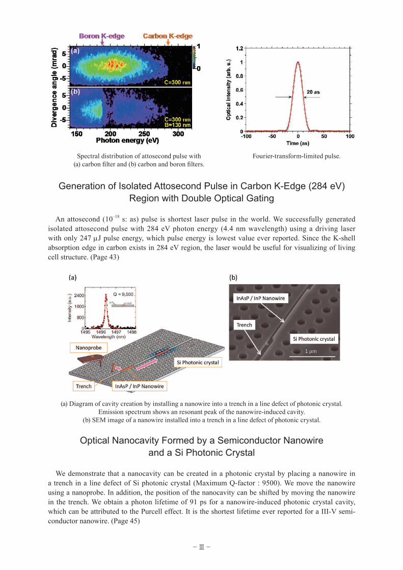
Spectral distribution of attosecond pulse with (a) carbon filter and (b) carbon and boron filters.
Fourier-transform-limited pulse.
Generation of Isolated Attosecond Pulse in Carbon K-Edge (284 eV) Region with Double Optical Gating
An attosecond (10–18 s: as) pulse is shortest laser pulse in the world. We successfully generated isolated attosecond pulse with 284 eV photon energy (4.4 nm wavelength) using a driving laser with only 247 µJ pulse energy, which pulse energy is lowest value ever reported. Since the K-shell absorption edge in carbon exists in 284 eV region, the laser would be useful for visualizing of living cell structure. (Page 43)
-Ⅲ-
(a) Diagram of cavity creation by installing a nanowire into a trench in a line defect of photonic crystal. Emission spectrum shows an resonant peak of the nanowire-induced cavity.
(b) SEM image of a nanowire installed into a trench in a line defect of photonic crystal.
Optical Nanocavity Formed by a Semiconductor Nanowireand a Si Photonic Crystal
We demonstrate that a nanocavity can be created in a photonic crystal by placing a nanowire in a trench in a line defect of Si photonic crystal (Maximum Q-factor : 9500). We move the nanowire using a nanoprobe. In addition, the position of the nanocavity can be shifted by moving the nanowire in the trench. We obtain a photon lifetime of 91 ps for a nanowire-induced photonic crystal cavity, which can be attributed to the Purcell effect. It is the shortest lifetime ever reported for a III-V semi-conductor nanowire. (Page 45)


Message from the Director
We at NTT Basic Research Laboratories (BRL) are extremely grateful for your interest and support with respect to our research activities. BRL’s missions are to promote progress in science and innovations in leading-edge technology to advance NTT's business. To achieve these missions, researchers in fields including physics, chemistry, biology, mathematics, electronics, informatics, and medicine, conduct basic research on materials science, physical science and optical science.
Since our management principle is based on an "open door" policy, we are collaborating with many universities and research institutes in Japan, US, Europe, and Asia as well as other NTT laboratories. NTT-BRL regularly organizes international conferences related to quantum physics and nanotechnology at NTT Atsugi R&D Center and
also holds a "Science Plaza" to enhance public understanding of our activities and to ensure a frank exchange of opinions. Moreover, one of our missions is the education of young researchers and we sponsor the biennial "BRL School", which boasts distinguished researchers as lecturers. In November 2013, thirty-five Ph.D. students and young researchers from universities and institutes in 14 countries participated in the BRL School.
These activities enable us to realize our missions with respect to the promotion of advances in science and the development of groundbreaking technology for NTT's business. Your continued support will be greatly appreciated.
July, 2014
Tetsuomi SogawaDirectorNTT Basic Research Laboratories
-Ⅴ-


Contentspage
◆ Cover♦ Sensing Fabric "hitoe" to Continuously Monitor Bioelectrical Signals
◆ Color Frontispiece ............................................................................................................Ⅰ♦ Annealing Paths of Pr2CuO4 and the Resulting Electronic Phase Diagrams♦ Coherent Phonon Manipulation in Coupled Mechanical Resonators♦ Encapsulated Gate-All-Around InAs Nanowire Field-Effect Transistors♦ Cluster State Generation for Ultracold Atoms in an Optical Lattice♦ Generation of Isolated Attosecond Pulse in Carbon K-Edge (284 eV) Region with Double
Optical Gating♦ Optical Nanocavity Formed by a Semiconductor Nanowire and a Si Photonic Crystal
◆ Message from the Director ................................................................................................Ⅴ
◆ NTT Basic Research Laboratories Organogram ................................................................ 1
◆ Member List ....................................................................................................................... 2
I. Research Topics
◇ Overview of Research in Laboratories ............................................................................................... 17
◇ Materials Science Laboratory ............................................................................................................ 19♦ Single-Crystal Cubic Boron Nitride Thin Film Growth by Ion-Beam-Assisted Molecular
Beam Epitaxy♦ Nucleus and Spiral Growth of N-face GaN (000-1) Obtained by Selective-Area Metalorganic
Vapor Phase Epitaxy♦ Enhanced Deep-UV Light Emission from Nonpolar M-plane AlGaN Quantum Wells♦ Superconductivity Hidden beneath Charge-Transfer Insulators♦ Broadening Light Emission at the Telecommunications Wavelengths by Material Engineering
of Rare-Earth Compounds on Silicon♦ Synthesis of Ultrathin Hexagonal Boron Nitride for Tunneling Applications♦ Thermal Instability of Graphene on a Substrate♦ Sensing Fabric "hitoe" to Continuously Monitor Bioelectrical Signals♦ Stable Sealing of Microcavities with a Lipid Membrane for Nanobiodevices♦ Ligand-Induced Structural Changes in a Single Ion Channel Receptor
◇ Physical Science Laboratory ............................................................................................................... 29♦ Fast and High-Sensitivity Charge Sensor Combined with a Resonance Circuit♦ Accuracy Evaluation of Si Single-Electron Transfer Devices at Extremely Low Temperature

♦ Coherent Phonon Manipulation in Coupled Mechanical Resonators♦ An Electromechanical Phonon Laser♦ Storage and Retrieval of Quantum States in a Hybrid Quantum System♦ Quantum State Projection with Various Measurement Strengths♦ Realizing Topological Insulating Phase in the Heterostructure Composed of Direct
Transition Band Gap Semiconductors♦ Encapsulated Gate-All-Around InAs Nanowire Field-Effect Transistors♦ AC Admittance of DNTT-Based MIS Capacitors
◇ Optical Science Laboratory ................................................................................................................ 38♦ Cluster State Generation for Ultracold Atoms in an Optical Lattice♦ An On-Chip Single Photon Buffer Based on Coupled Resonator Optical Waveguide♦ Long-Term Performance of Quantum Key Distribution over 90-km Optical Links Installed
in a Field Environment of Tokyo Metropolitan Area♦ Growth of InP Nanowires on Graphene-Covered Fe♦ Topological Raman Band in the Carbon Nanohorn♦ Generation of Isolated Attosecond Pulse in Carbon K-Edge (284 eV) Region with Double
Optical Gating♦ Modification of Exciton Optical Properties with Coherent Phonons in Quantum Dots♦ Optical Nanocavity Formed by a Semiconductor Nanowire and a Si Photonic Crystal♦ InGaAs Photodetectors Based on Photonic Crystal Waveguide Including Ultrasmall Buried
Heterostructure♦ Enhanced and Suppressed Spontaneous Emission from a Buried Heterostructure Photonic
Crystal Cavity
◇ Nanophotonics Center ........................................................................................................................ 48♦ Low Energy Consumption Direct Modulation of Lambda-Scale Embedded Active-Region
Photonic-Crystal Lasers♦ Significant L-Band Responsivity Improvement of Germanium Waveguide Photodiode by
Franz-Keldysh Effect
II. Data
◇ 6th NTT-BRL School ...................................................................................................................... 51
◇ International Symposium on Nanoscale Transport and Technology (ISNTT 2013) ....................... 52
◇ List of BRL Seminars (Fiscal 2013) ................................................................................................... 53
◇ Award Winners’ List (Fiscal 2013) ................................................................................................. 56
◇ In-house Award Winners’ List (Fiscal 2013) .................................................................................. 57
◇ Numbers of Papers, Presentations and Patents (2013) ................................................................... 58
◇ List of Invited Talks at International Conferences (2013) .............................................................. 60

1Research Activities in NTT Basic Research Laboratories Vol. 24 (2013)
NTT Basic Research Laboratories OrganogramAs of March 31, 2014
Director
Tetsuomi Sogawa, Dr.
Quantum and Nano Device Research
Senior Distinguished Researcher
Hiroshi Yamaguchi, Dr.
Research Planning Section
Executive Manager
Hideki Yamamoto, Dr.
Physical Science Laboratory
Executive Manager
Akira Fujiwara, Dr.
Materials Science Laboratory
Executive Manager
Hiroki Hibino, Dr.
Optical Science Laboratory
Executive Manager
Tetsuomi Sogawa, Dr.
Nanophotonics Center
Executive Manager
Masaya Notomi, Dr.

2 Research Activities in NTT Basic Research Laboratories Vol. 24 (2013)
Member List
As of March 31, 2014(*/ left NTT BRL during the year)
NTT Basic Research Laboratories
Director, Dr. Tetsuomi Sogawa
Quantum and Nano Device Research
Senior Distinguished Researcher, Dr. Hiroshi Yamaguchi
Research Planning Section
Executive Research Scientist, Dr. Hideki Yamamoto
Senior Research Scientist, Dr. Hiroshi Nakashima
Senior Research Scientist, Dr. Katsuya Oguri
NTT Research Professor Prof. Yasuhiro Tokura (University of Tsukuba)
3Research Activities in NTT Basic Research Laboratories Vol. 24 (2013)
Materials Science Laboratory
Executive Manager, Dr. Hiroki Hibino
Dr. Tetsuya Akasaka
Thin-Film Materials Research Group: Dr. Hideki Yamamoto (Group Leader) Dr. Yasuyuki Kobayashi* Dr. Kazuhide Kumakura Dr. Hisashi Sato Dr. Tetsuya Akasaka Dr. Yoshitaka Taniyasu Dr. Koji Onomitsu Dr. Yoshiharu Krockenberger Dr. Shin-ichi Karimoto Dr. Masanobu Hiroki Dr. Kazuyuki Hirama Dr. Chia-Hung Lin Dr. Ryan Banal
Low-Dimensional Nanomaterials Research Group: Dr. Hiroki Hibino (Group Leader) Dr. Fumihiko Maeda Dr. Kazuaki Furukawa Dr. Satoru Suzuki Dr. Hiroo Omi Dr. Yuko Ueno Dr. Yoshiaki Sekine Dr. Shin-ichi Tanabe* Dr. Makoto Takamura Dr. Shengnan Wang Dr. Yuya Murata* Dr. Carlo M. Orofeo Dr. Adel Najar
Molecular and Bio Science Research Group: Dr. Koji Sumitomo (Group Leader) Dr. Shingo Tsukada Dr. Nahoko Kasai Dr. Yoshiaki Kashimura Dr. Touichiro Goto Dr. Aya Tanaka Dr. Azusa Oshima

4 Research Activities in NTT Basic Research Laboratories Vol. 24 (2013)
Physical Science Laboratory
Executive Manager, Dr. Akira Fujiwara
Dr. Toshiaki Hayashi
Takeshi Karasawa
Nanodevices Research Group: Dr. Akira Fujiwara (Group Leader) Dr. Hiroyuki Kageshima Toru Yamaguchi Dr. Katsuhiko Nishiguchi Hirotaka Tanaka Dr. Jin-ichiro Noborisaka Dr. Gento Yamahata Dr. Kensaku Chida
Hybrid Nanostructure Physics Research Group: Dr. Hiroshi Yamaguchi (Group Leader) Dr. Yuichi Harada Dr. Hayato Nakano Dr. Kenji Yamazaki Dr. Shiro Saito Dr. Masumi Yamaguchi* Dr. Imran Mahboob Dr. Hajime Okamoto Dr. Kousuke Kakuyanagi Dr. Yuichiro Matsuzaki Daiki Hatanaka Dr. Hiraku Toida Dr. Yuma Okazaki
Quantum Solid State Physics Research Group: Dr. Koji Muraki (Group Leader) Dr. Kiyoshi Kanisawa Dr. Satoshi Sasaki Dr. Hiroyuki Tamura Dr. Kyoichi Suzuki Dr. Toshiaki Hayashi Dr. Takeshi Ohta Dr. Norio Kumada Dr. Keiko Takase Dr. Hiroshi Irie Dr. Takashi Kobayashi* Dr. Trevor David Rhone

5Research Activities in NTT Basic Research Laboratories Vol. 24 (2013)
Optical Science Laboratory
Executive Manager, Dr. Tetsuomi Sogawa
Dr. Tetsuya Mukai
Quantum Optical State Control Research Group: Dr. Kaoru Shimizu (Group Leader) Dr. Hiroki Takesue Dr. Masami Kumagai Kazuhiro Igeta Dr. Hiroyuki Shibata Dr. Makoto Yamashita Dr. Tetsuya Mukai Dr. Fumiaki Morikoshi Dr. Kiyoshi Tamaki Dr. Kensuke Inaba Daisuke Hashimoto Dr. Nobuyuki Matsuda Dr. Koji Azuma Dr. Hiromitsu Imai Dr. Takahiro Inagaki Dr. William John Munro Dr. Kazuto Noda
Quantum Optical Physics Research Group: Dr. Hideki Gotoh (Group Leader) Dr. Kouta Tateno Dr. Takehiko Tawara Dr. Atsushi Ishizawa Dr. Guoquiang Zhang Dr. Haruki Sanada Dr. Keiko Kato Dr. Hiroki Mashiko Dr. Ken-ichi Hitachi Dr. Yoji Kunihashi Dr. Ken-ichi Sasaki
Photonic Nano-Structure Research Group: Dr. Masaya Notomi (Group Leader) Dr. Akihiko Shinya Dr. Atsushi Yokoo Dr. Eiichi Kuramochi Dr. Hideaki Taniyama Dr. Hisashi Sumikura Dr. Kengo Nozaki Dr. Masato Takiguchi Dr. Masaaki Ono Dr. Danang Birowosuto* Dr. Hao Xu* Dr. Abdul Shakoor
6 Research Activities in NTT Basic Research Laboratories Vol. 24 (2013)
Nanophotonics Center
Executive Manager, Dr. Masaya Notomi
Photonic Nano-Structure Research Team: Dr. Masaya Notomi Dr. Akihiko Shinya Dr. Atsushi Yokoo Dr. Eiichi Kuramochi Dr. Hideaki Taniyama Dr. Hisashi Sumikura Dr. Kengo Nozaki Dr. Masato Takiguchi Dr. Masaaki Ono Dr. Hiroo Omi Dr. Takehiko Tawara Dr. Hiroyuki Shibata Dr. Nobuyuki Matsuda
InP Compound Device Research Team: Dr. Shinji Matsuo Dr. Takaaki Kakitsuka Tomonari Sato Dr. Koji Takeda Dr. Koichi Hasebe Takuro Fujii
Silicon Photonics Research Team: Dr. Koji Yamada Dr. Tai Tsuchizawa Rai Kou (Rai Takahashi) Hidetaka Nishi Tatsurou Hiraki Dr. Kotarou Takeda

7Research Activities in NTT Basic Research Laboratories Vol. 24 (2013)
Senior Distinguished Researcher
Masaya Notomi was born in Kumamoto, Japan, on 16 February 1964. He received his B.E., M.E. and Ph.D. degrees in applied physics from University of Tokyo, Japan in 1986, 1988, and 1997, respectively. In 1988, he joined NTT Optoelectronics Laboratories. Since then, his research interest has been to control the optical properties of materials and devices by using artificial nanostructures, and engaged in research on quantum wires/dots and photonic crystal structures. He has been in NTT Basic Research Laboratories since 1999, and currently a group leader of Photonic Nanostructure Research Group and a director of NTT Nanophotonics Center. He is also entitled as Senior Distinguished Scientist of NTT since 2010. In 1996-1997, he was a visiting researcher of Linköping University (Sweden). He was a guest associate professor of Applied Electronics in 2003-2009 and is currently a guest professor of Physics in Tokyo Institute of Technology. He received IEEE/LEOS Distinguished Lecturer Award in 2006, JSPS (Japan Society for the Promotion of Science) prize in 2009, Japan Academy Medal in 2009, The Commendation for Science and Technology by the Minister of Education, Culture, Sports, Science and Technology (Prize for Science and Technology, Research Category) in 2010, and IEEE Fellow grade in 2013. He is serving as a member of National University Corporation Evaluation Committee in the Japanese government. He is also a member of the Japan Society of Applied Physics, APS, IEEE, and OSA.
Hiroshi Yamaguchi was born in Osaka Japan on October 30, 1961. He received the B.E., M.S. in physics and Ph.D. degrees in engineering from the Osaka University in 1984, 1986 and 1993, respectively. He joined NTT Basic Research Laboratories in 1986 and has engaged in the study of compound semiconductor surfaces using electron diffraction and scanning tunneling microscopy. His current interests are micro/nanomechanical devices using semiconductor heterostructures. He was a visiting research fellow in Imperial College, University of London, U.K. during 1995-1996 and a visiting research staff in Paul Drude Institute, Germany in 2003. He is a guest professor in Tohoku University from 2006 and a director of the Japanese Society of Applied Physics (JSAP) in 2008 and 2009. He served as more than 40 committee members of academic societies and international conferences. He received JSAP Fellowship (2013), Commendation for Science and Technology by MEXT (2013), Inoue Prize for Science (2012), Institute of Physics (IOP) Fellowship (2011), SSDM2009 Paper Award (2010), MNC2008 Outstanding Paper Award (2009), and the Paper Awards of Japan Society of Applied Physics (1989, 2004, 2010). He is currently an executive manager of Quantum and Nano Device Research and a group leader of Hybrid Nanostructure Physics Research Group. He is a member of JSAP, the Physical Society of Japan, IOP, American Physical Society (APS), and IEEE.

8 Research Activities in NTT Basic Research Laboratories Vol. 24 (2013)
Koji Muraki was born in Tokyo, Japan in 1965. He received his B.S., M.S., and Ph.D. degrees in applied physics from The University of Tokyo, Japan, in 1989, 1991, and 1994, respectively. In 1994, he joined Basic Research Laboratories, Nippon Telegraph and Telephone (NTT) Corporation, Kanagawa, Japan. Since then, he has been engaged in the growth of high-mobility heterostructures and the study of highly correlated electronic states realized in such structures. He was a guest researcher at Max-Planck Institute, Stuttgart, Germany during 2001-2002. He served as a program committee/chair of international conferences on High Magnetic Fields in Semiconductor Physics (HMF) and Electronic Properties of Two-Dimensional Systems (EP2DS). He was a leader of physics research and epitaxy group of ERATO Nuclear Spin Electronics Project, Japan Science and Technology, during 2008-2013. He was appointed as Distinguished Scientist of NTT in 2009 and Senior Distinguished Scientist of NTT in 2013. He is a member of the Physical Society of Japan and Japan Society of Applied Physics.

9Research Activities in NTT Basic Research Laboratories Vol. 24 (2013)
Distinguished Researchers
Akira Fujiwara was born in Tokyo, Japan in 1967. He received his B.S., M.S., and Ph.D. degrees in applied physics from The University of Tokyo, Japan in 1989, 1991, and 1994, respectively. In 1994, he joined NTT LSI Laboratories and moved to NTT Basic Research Laboratories in 1996. Since 1994, he has been engaged in research on silicon nanostructures and their application to single-electron devices. He is a senior manager of Physical Science Laboratory and a group leader of Nanodevices Research Group since April 2012. He was a guest researcher at the National Institute of Standards and Technology (NIST), Gaithersburg, MD, USA during 2003-2004. He was a director of the Japanese Society of Applied Physics in 2010 and 2011 and a visiting professor of Hokkaido University in 2013. He received the SSDM Young Researcher Award in 1998, SSDM Paper Award in 1999, and Japanese Journal of Applied Physics (JJAP) Paper Awards in 2003 , 2006, and 2013. He was awarded the Young Scientist Award from the Minister of MEXT (Ministry of Education, Culture, Sports, Science, and Technology) in 2006. He is a member of the Japan Society of Applied Physics and the IEEE.
Yoshitaka Taniyasu was born in Toyama, Japan on June 10, 1973. He received his B.E., M.E., and Dr. Eng. degrees in electrical engineering from Chiba University, Chiba, Japan in 1996, 1998, and 2001, respectively. He joined NTT Basic Research Laboratories in 2001. He has been engaged in research on wide-bandgap nitride semiconductors. He was a visiting researcher at Ecole polytechnique fédérale de Lausanne (EPFL) during 2011-2012. He received the Young Scientist Award for the Presentation of the Excellent Paper at the Japan Society of Applied Physics (JSAP) in 2001, the Young Scientist Award at the 14th Semiconducting and Insulating Materials Conference in 2007, the Young Scientists’ Prize from the Minister of Education, Culture, Sports, Science and Technology, the Young Scientist Award at the 38th International Symposium on Compound Semiconductors in 2011, and the Best Paper Award at the International Workshop on Nitride Semiconductors in 2012. He is a member of the JSAP.
Norio Kumada was born in Gifu, Japan in 1975. He received his B.S., M.S., and Ph.D. degrees in physics from Tohoku University, Japan, in 1998, 2000, and 2003, respectively. In 2003, he joined NTT Basic Research Laboratories, Kanagawa, Japan. Since then, he has been engaged in the study of highly correlated electronic states realized in semiconductor heterostructures. He received Young Scientist Award of the Physical Society of Japan in 2008, and the Young Scientists’ Prize from the Minister of Education, Culture, Sports, Science and Technology in 2012. He is a member of the Physical Society of Japan.

10 Research Activities in NTT Basic Research Laboratories Vol. 24 (2013)
Katsuhiko Nishiguchi was born in Hiroshima, Japan in 1975. He received the B.E., M.E., and Ph.D. in electrical engineering in 1998, 2000, and 2002, respectively, from Tokyo Institute of Technology, Tokyo, Japan. Since joining NTT Basic Research Laboratories in 2002, he has been engaged in the research on physics and technology of Si nanometer-scale devices for LSI applications with low power consumption and new functions. He was an invited researcher at the National Center for Scientific Research (CNRS), France during September 2008 and also a guest researcher at Delft University of Technology, Delft, the Netherlands during 2012-2013. He received IUPAP Young Author Best Paper Award at the International Conference on Physics of Semiconductors 2000, Graduate Student Award Silver at the Materials Research Society 2000 Fall Meeting, Young Scientist Award at the Japan Society of Applied Physics Spring Meeting in 2000, JSAP Outstanding Paper Award 2013, and The Commendation for Science and Technology by the Minister of Education, Culture, Sports, Science and Technology of Japan (The Young Scientists' Prize) in 2013. He is a member of the Japan Society of Applied Physics.
Shiro Saito was born in Tokyo, Japan in 1972. He received his B.S., M.S., and Dr. Eng. degrees in applied physics from the University of Tokyo, Japan, in 1995, 1997, and 2000, respectively. In 2000, he joined NTT Basic Research Laboratories, Nippon Telegraph and Telephone Corporation, Kanagawa, Japan. Since then, he has been engaged in quantum information processing using superconducting circuits. He was a guest researcher at Delft University of Technology, Delft, the Netherlands during 2005-2006. He received Young Scientist Award at the Japan Society of Applied Physics Spring Meeting in 2004. He is a guest associate professor in Tokyo University of Science from 2012. He is a member of the Physical Society of Japan and the Japan Society of Applied Physics.
Hiroki Takesue was born in Wakayama, Japan, on May 10, 1971. He received B.E., M.E., and Ph.D. degrees in engineering science from Osaka University, Osaka, Japan, in 1994, 1996, and 2002, respectively. In 1996, he joined NTT Access Network Systems Laboratories, Ibaraki, Japan, where he engaged in research on optical access networks using wavelength division multiplexing. In 2003, he moved to NTT Basic Research Laboratories, Atsugi, Japan. Since then, he has been engaged in experimental quantum optics and quantum communications. He is the recipient of several awards, including the ITU-T Kaleidoscope Conference 2nd Best Paper Award in 2008 and The Commendation for Science and Technology by the Minister of Education, Culture, Sports, Science and Technology of Japan (The Young Scientists' Prize) in 2010. From 2004 to 2005, he was a Visiting Scholar at Stanford University, Stanford, CA. He is a member of IEEE and the Japan Society of Applied Physics.

11Research Activities in NTT Basic Research Laboratories Vol. 24 (2013)
Imran Mahboob was born in Sheffield, England on 20 April, 1978. He received a combined B.Sc. and M.Sc. degree in Theoretical Physics from The University of Sheffield in 2001 and Ph.D. degree in Physics studying the electronic properties of nitride semiconductors from The University of Warwick in 2004. He joined NTT Basic Research Laboratories in 2005 as a Research Associate, from 2008 as a Research Specialist, and from 2012 as a Senior Research Scientist. His current interests are developing electromechanical resonators for digital signal processing applications and to study their non-linear dynamics. He received the Clarke Prize in Physics from the University of Sheffield in 2001 and the Young Scientist Award at the 2003 Physics of Semiconductors and Interfaces conference.

12 Research Activities in NTT Basic Research Laboratories Vol. 24 (2013)
Advisory Board (2013 Fiscal Year)
Name Affiliation
Prof. Gerhard Abstreiter Walter Schottky Institute, Technical University of Munich, Germany
Prof. John Clarke Department of Physics, University of California, Berkeley, U.S.A.
Prof. Evelyn Hu School of Engineering and Applied Sciences, Harvard University, U.S.A.
Prof. Mats Jonson Department of Physics, University of Gothenburg, Sweden
Prof. Sir Peter Knight Department of Physics, Imperial College/The Kavli Royal Society International Centre at Chicheley Hall, U.K.
Prof. Anthony J. Leggett Department of Physics, University of Illinois, U.S.A.
Prof. Allan H. MacDonald Department of Physics, The University of Texas, Austin, U.S.A.
Prof. Andreas Offenhäusser Institute of Complex Systems, Forschungszentrum Julich, Germany
Prof. Halina Rubinsztein-Dunlop School of Physical Sciences, University of Queensland, Australia
Prof. Klaus von Klitzing Max Planck Institute for Solid State Research, Germany

13Research Activities in NTT Basic Research Laboratories Vol. 24 (2013)
Invited / Guest Scientists (2013 Fiscal Year)
Name Affiliation Period
Prof. Koichi Semba National Institute of Informatics (NII), Apr. 2013 – Mar. 2014 Japan
Overseas Trainees (2013 Fiscal Year)
Name Affiliation Period
Ruaridh Forbes University of Edinburgh, U.K. Jul. 2012 – Apr. 2013
Pawel Pactwa AGH University of Science and Techonology, Poland
Sep. 2012 – Aug. 2013
Justin Yan The University of British Columbia, Canada Jan. 2013 – Aug. 2013
Thomas Ziebarth University of Victoria, Canada Jan. 2013 – Aug. 2013
Joey Chau University of Toronto, Canada Jan. 2013 – Dec. 2013
Punn Augsornworawat McGill University, Canada Jan. 2013 – Dec. 2013
Amedee Lacraz ESPCI ParisTech (École supérieure de physique et de chimie industrielles de la ville de Paris), France
Apr. 2013 – Aug. 2013
Anthony Park The University of British Columbia, Canada May 2013 – Dec. 2013
Jing Wang Georgia Institute of Technology, U.S.A. May 2013 – Dec. 2013
Samuel Metais ESPCI ParisTech (École supérieure de physique et de chimie industrielles de la ville de Paris), France
Jul. 2013 – Dec. 2013

14 Research Activities in NTT Basic Research Laboratories Vol. 24 (2013)
Name Affiliation Period
Simon Yves ESPCI ParisTech (École supérieure de physique et de chimie industrielles de la ville de Paris), France
Jul. 2013 – Dec. 2013
Nicolas Perrissin ESPCI ParisTech (École supérieure de physique et de chimie industrielles de la ville de Paris), France
Jul. 2013 – Dec. 2013
Malo Tarpin ESPCI ParisTech (École supérieure de physique et de chimie industrielles de la ville de Paris), France
Jul. 2013 – Dec. 2013
Sophie De La Vaissiere ESPCI ParisTech (École supérieure de physique et de chimie industrielles de la ville de Paris), France
Jul. 2013 – Dec. 2013
Louise Waterston University of Edinburgh, U.K. Jul. 2013 –
Paul Knott University of Leeds, U.K. Sep. 2013 – Dec. 2013
Rick Lu University of Waterloo, Canada Sep. 2013 –
Anna Fomitcheva Khartchenko
University of Barcelona, Spain Sep. 2013 –
Jose Alberto Rodriguez Santamaria
University of Burgos, Germany Sep. 2013 –
Krzysztof Jan Gibasiewicz
Warsaw university of Technology, Poland Sep. 2013 –
Gianfranco D'Ambrosio Politecnico di Milano, Italy Sep. 2013 –
Logan G. Blackstad Georgia Institute of Technology, U.S.A. Sep. 2013 –
Peter Karkus Budapest University of Technology and Economics, Hungary
Sep. 2013 –
Henry Pigot The University of British Columbia, Canada Jan. 2014 –
Ryan Neufeld University of Waterloo, Canada Jan. 2014 –
Adrian Salmon Georgia Institute of Technology, U.S.A. Jan. 2014 –
Andrew Tin McGill University, Canada Feb. 2014 –

15Research Activities in NTT Basic Research Laboratories Vol. 24 (2013)
Domestic Trainees (2013 Fiscal Year)
Name Affiliation Period
Shun Dai The University of Tokyo Apr. 2013 – Mar. 2014
Rento Osugi Tohoku University Apr. 2013 – Mar. 2014
Shunichi Matsumoto Tokyo University of Science Apr. 2013 – Mar. 2014
Hajime Suzuki Tokyo University of Science Apr. 2013 – Mar. 2014
Takahiko Sato The University of Tokyo Apr. 2013 – Mar. 2014
Nuremy Binti Che Ani Tokyo Denki University Apr. 2013 – Mar. 2014
Takahiro Gotoh Tokyo Denki University Apr. 2013 – Mar. 2014
Keisuke Noguchi Tokyo Institute of Technology Apr. 2013 – Mar. 2014
Takanobu Tsunoi Yokohama National University Apr. 2013 – Mar. 2014
Tomohiko Yamaguchi Tokyo University of Science Apr. 2013 – Mar. 2014
Toru Tanaka Waseda University Apr. 2013 – Mar. 2014
Ahmad Yoshinari Tokyo University of Science May 2013 – Mar. 2014
Ken-ichi Suzuki Tokyo Denki University Jun. 2013 – Mar. 2014
Akihiro Fushimi Keio University Jun. 2013 – Mar. 2014
Saki Tanaka Keio University Jul. 2013 – Aug. 2013
Kenta Inoue University of Tsukuba Aug. 2013 – Sep. 2013
Han Cai Tohoku University Oct. 2013 – Mar. 2014
Kazuki Moriya The University of Tokyo Oct. 2013 – Mar. 2014
Shingo Kanouchi Nagaoka University of Technology Oct. 2013 – Feb. 2014
Shouhei Takagi Nagaoka University of Technology Oct. 2013 – Feb. 2014
Saki Tanaka Keio University Oct. 2013 – Mar. 2014
Teo Dong Sheng Toyohashi University of Technology Jan. 2013 – Feb. 2014
Tomohiro Tamaki Toyo University Jan. 2013 – Mar. 2014


Ⅰ.Research Topics

17Research Activities in NTT Basic Research Laboratories Vol. 24 (2013)
Overview of Research in Laboratories
Materials Science Laboratory Hiroki Hibino
This laboratory aims at contributing to progress in materials science and revolutionizing information communication technology by creating new materials and functions through materials design at the atomic and molecular levels. This laboratory consists of three research groups investigating a wide range of materials such as nitride semiconductors, graphene, superconductors, and biological molecules. We are conducting innovative materials research based on the technologies of growing high-quality thin films and precisely measuring the structure and physical properties of materials. This year, we succeeded in clarifying microscopic state changes during the annealing treatment which induces superconductivity in undoped cuprates so far believed as insulators and growing single-crystal cubic BN thin film on diamond and single-layer hexagonal BN on Co films, respectively. We also succeeded in developing new sensing fabric "hitoe", which enables to acquire biomedical signals by simply wearing the clothes, in collaboration with Toray Industries, Inc.
Physical Science Laboratory Akira Fujiwara
The aim of this laboratory is to develop semiconductor- and superconductor-based solid- state devices, which will have a revolutionary impact on future communication and information technologies. Utilizing high-quality crystal growth techniques and nanolithography techniques we have developed, research groups in our laboratory are working on nanodevices, quantum information processing devices, and high-sensitivity sensors based on new degrees of freedom such as single electrons, mechanical oscillations, quantum coherent states, and spins. This year we succeeded in realizing phonon lasing in an electromechanical resonator and coherent phonon manipulation in coupled mechanical resonators. We also demonstrated storage and readout of quantum states in a superconductor/diamond hybrid system. Progress was made in the research on topological insulating phase in InAs/GaSb heterostructures, accuracy evaluation of single-electron transfer, FET sensors with a resonance circuit, and gate overlapped InAs nanowire FETs.

18 Research Activities in NTT Basic Research Laboratories Vol. 24 (2013)
Optical Science Laboratory Tetsuomi Sogawa
This laboratory aims for the development of core-technologies that will innovate on optical communications and optical signal processing, and seeks fundamental scientific progresses. The groups in our laboratory are working for the quantum state control by very weak light, the search for intriguing phenomena using very intensive and short pulse light, and control of optical properties by using photonic crystals and ultrasonic techniques, based on unique properties of semiconductor nanostructures such as quantum dots and nanowires. In this year, we achieved an on-chip single photon buffer by using a coupled resonator optical waveguide based on silicon photonic crystal cavities. We examined the long-term operation performance of a long-distance (90 km) differential phase shift key distribution service using a test-bed optical network in the Tokyo metropolitan area. We also proposed that a very high-fidelity entangled cluster state can be formed with a combination of laser irradiation and intensity tuning. In addition, we have successfully demonstrated control of excitonic optical properties in quantum dots by using coherent phonons and generation of an isolated attosecond pulse in Carbon K-edge (284 eV) region with a double optical gating method.
Nanophotonics Center Masaya Notomi
Nanophotonics Center (NPC) was established in April 2012 by several research groups involved with nanophotonics in Basic Research Laboratories, Photonics Laboratories, and Microsystem Integration Laboratories in NTT. We are aiming for developing a full-fledged large-scale photonic integration technology by which we will be able to densely integrate a large number of nano-scale photonic devices with various functions in a single chip. Furthermore, we are targeting extreme reduction of the consumption energy for photonic information processing by taking advantage of the nanophotonics technology. This year, we demonstrated a novel way to form a nanocavity by placing a III/V semiconductor nanowire on a Si photonic crystal, and we also realized a novel multi-layer waveguide on Si for mode-division multiplexing. As regards nanophotonic device research, we have realized a novel nano-photodetector based on photonic crystals, and succeeded in largely reducing the operation energy-per-bit of electrically-pumped nanolasers. In addition, we achieved accelerated spontaneous emission rate of quantum wells in photonic crystal nanocavities.

19Research Activities in NTT Basic Research Laboratories Vol. 24 (2013)
Fig. 1. Cross-sectional TEM and SAED images of single-crystal c-BN(001).
Fig. 2. RHEED pattern of single-crystal c-BN(001).
Fig. 3. Phase diagram of BN films in ion-beam-assisted MBE process.
Single-Crystal Cubic Boron Nitride Thin Film Growthby Ion-Beam-Assisted Molecular Beam Epitaxy
Kazuyuki Hirama, Yoshitaka Taniyasu, Shin-ichi Karimoto, Yoshiharu Krockenberger, and Hideki Yamamoto
Materials Science Laboratory
Cubic boron nitride (c-BN) with sp3-bonding has a large bandgap energy of 6.25 eV and a high breakdown field of ~ 8 MV/cm, which may further expand the potential of nitride-based semiconductor devices. However, conventional growth methods for group-III nitrides, such as MOVPE, have been unsuccessful in the growth of single-crystal c-BN films because c-BN is a metastable phase at ambient atmosphere. Here we report the epitaxial growth of single-crystal c-BN films by the ion-beam-assisted molecular beam epitaxy (MBE) method. We show that a proper adjustment of acceleration voltage for N2
+ and Ar+ ions is the key to the selective formation of the c-BN phase. BN thin films were grown on diamond(001) substrates by electron-beam evaporation of B in a flux of N2
+ and Ar+ ions. The acceleration voltage (Vacc) for the ions was varied in the range from 200 to 450 V. The growth temperature (Tg) was varied in the range from 400 to 820oC. The supplied nitrogen/boron ratio was set at values > 1. Single-crystal c-BN(001) films were obtained at Tg ≥ 750oC with Vacc = 280 V. The formation of the single-crystal c-BN was confirmed by cross-sectional TEM, selective area electron diffraction (SAED) and RHEED (Figs. 1 and 2) [1]. Although the designated thickness of the c-BN film was 160 nm, the resultant c-BN films were about 30-nm thick. This means that ~ 80 % of supplied B atoms were etched by ion bombardments during the c-BN growth. To obtain a clue to the growth mechanism of c-BN in the ion-beam-assisted MBE processes, we also carried out regrowth of BN films on single-crystal c-BN thin film templates on diamond substrates with the growth parameters systematically varied. A summary of those results provided us a phase diagram of BN, which was plotted as a function of Vacc and Tg (Fig. 3). The phase diagram indicates a strong dependence on Vacc with much less dependence on Tg. At Vacc < 220 V (Region I), sp2-bonded turbostratic BN (t-BN) is predominantly formed. At Vacc between 220 and 450 V (Region II), single-crystal c-BN continues to grow. At Vacc > 450 V (Region III), the c-BN template is etched out as evidenced by an instantaneous change of the RHEED pattern back to that of the diamond(001) substrate. In short, at low acceleration voltages, sp2-bonded BN is dominantly formed, while at high acceleration voltages, etching dominates, irrespective of the bonding characteristics of BN. Consequently, the formation and epitaxial growth of metastable c-BN are achieved as a result of the interplay between competitive phase formation and selective etching [1]. This work was supported by KAKENHI.[1] K. Hirama et al., Appl. Phys. Lett. 104 (2014) 092113.

20 Research Activities in NTT Basic Research Laboratories Vol. 24 (2013)
Fig. 1. Atomic force microscopic image of an almost step-free N-face GaN (000–1) surface. Vertical stripes are due to the optical noise.
Fig. 2. Nucleus and spiral growth rate of GaN plotted as a function of TMG flow rate.
Nucleus and Spiral Growth of N-face GaN (000-1)Obtained by Selective-Area Metalorganic Vapor Phase Epitaxy
Chia-Hung Lin, Tetsuya Akasaka, and Hideki YamamotoMaterials Science Laboratory
Step-free surfaces without any fluctuation of thickness are promising for developing high-performance quantum devices with abrupt hetero-interfaces. We have recently succeeded in preparing a step-free Ga-face GaN (0001) surface by selective-area metalorganic vapor phase epitaxy (SA-MOVPE) [1]. An N-face GaN (000–1) surface is also attractive for obtaining high-quality InN and InxGa1–xN films because of its higher affinity to N. However, it is difficult to achieve an atomically smooth N-face GaN (000–1) surface since the surface usually contains a high density of hexagonal hillocks. In this study, we investigated the formation of a step-free N-face GaN (000–1) surface using SA-MOVPE. GaN films were grown selectively on an N-face GaN (000–1) bulk substrate covered by SiO2 masks with a set of hexagonal openings 16 μm in diameter. Source gases were trimethylgallium (TMG) and NH3, and purified H2 was the carrier gas. The NH3 flow rate was kept at 6.7x10⁻² mol/min, while the TMG flow rate was varied from 9.7 to 20.8 μmol/min. The growth temperature was 1015oC. Figure 1 shows an almost step-free N-face GaN (000–1) surface with few atomic steps. The surface was formed by two-dimensional (2D) nucleus growth in the absence of screw-type dislocations (STDs) within a hexagonal opening. Meanwhile, in the same sample, growth spirals with atomic steps were also observed within another hexagonal opening having STDs. Figure 2 shows nucleus and spiral growth rates of GaN plotted as a function of the TMG flow rate. The nucleus growth rates are all very low even for a higher TMG flow rate, whereas spiral growth ones increase rapidly with increasing TMG flow rate [2]. The slow growth rates in 2D nucleus growth indicate that the growth proceeds under low surface supersaturation, which results in an extremely low 2D nucleus density. The low 2D nucleus density is considered a key factor for achieving a step-free N-face GaN (000–1) surface. This work was partly supported by KAKENHI.
[1] T. Akasaka, Y. Kobayashi, and M. Kasu, Appl. Phys. Express 2 (2009) 091002.[2] C.H. Lin, T. Akasaka, and H. Yamamoto, Appl. Phys. Express 6 (2013) 035503.
21Research Activities in NTT Basic Research Laboratories Vol. 24 (2013)
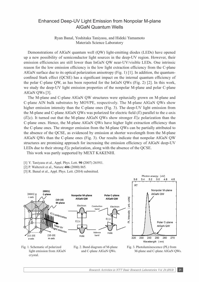
Fig. 1. Schematic of polarized light emission from AlGaN crystal.
Fig. 2. Band diagram of M-plane and C-plane AlGaN QWs.
Fig. 3. Photoluminescence (PL) from M-plane and C-plane AlGaN QWs.
Enhanced Deep-UV Light Emission from Nonpolar M-planeAlGaN Quantum Wells
Ryan Banal, Yoshitaka Taniyasu, and Hideki YamamotoMaterials Science Laboratory
Demonstrations of AlGaN quantum well (QW) light-emitting diodes (LEDs) have opened up a new possibility of semiconductor light sources in the deep-UV region. However, their emission efficiencies are still lower than InGaN QW near-UV/visible LEDs. One intrinsic reason for the low emission efficiency is the low light extraction efficiency from the C-plane AlGaN surface due to its optical polarization anisotropy (Fig. 1) [1]. In addition, the quantum-confined Stark effect (QCSE) has a significant impact on the internal quantum efficiency of the polar C-plane QW, as has been reported for the InGaN QWs (Fig. 2) [2]. In this work, we study the deep-UV light emission properties of the nonpolar M-plane and polar C-plane AlGaN QWs [3]. The M-plane and C-plane AlGaN QW structures were epitaxially grown on M-plane and C-plane AlN bulk substrates by MOVPE, respectively. The M-plane AlGaN QWs show higher emission intensity than the C-plane ones (Fig. 3). The deep-UV light emission from the M-plane and C-plane AlGaN QWs was polarized for electric field (E) parallel to the c-axis (E||c). It turned out that the M-plane AlGaN QWs show stronger E||c polarization than the C-plane ones. Hence, the M-plane AlGaN QWs have higher light extraction efficiency than the C-plane ones. The stronger emission from the M-plane QWs can be partially attributed to the absence of the QCSE, as evidenced by emission at shorter wavelength from the M-plane AlGaN QWs than the C-plane ones (Fig. 3). Our results indicate that nonpolar AlGaN QW structures are promising approach for increasing the emission efficiency of AlGaN deep-UV LEDs due to their strong E||c polarization, along with the absence of the QCSE. This work was partly supported by MEXT KAKENHI.
[1] Y. Taniyasu et al., Appl. Phys. Lett. 90 (2007) 261911.[2] P. Waltereit et al., Nature 406 (2000) 865.[3] R. Banal et al., Appl. Phys. Lett. (2014) submitted.

22 Research Activities in NTT Basic Research Laboratories Vol. 24 (2013)
Superconductivity Hidden beneath Charge-Transfer Insulators
Yoshiharu Krockenberger, and Hideki YamamotoMaterials Science Laboratory
High temperature superconductivity (HTS) remains a mystery. For hole-doped cuprate superconductors doping is sufficient to induce superconductivity but such an approach does not hold for electron-doped cuprates. Moreover, while hole-doped cuprates are a build-up of CuO2 planes with copper being either five- or six-fold coordinated, electron doping only works when copper is four-fold coordinated. The fact that an annealing procedure is mandatory for the induction of superconductivity in cuprates with square-planar coordinated copper has obscured physicists for long while, hampering the development of effective theoretical models describing superconductivity in cuprates. Since the electron-doped side of the electronic phase diagram represents not only the quantity of doped electrons but to a much higher extent the influence of annealing, it is about time to liberate the phase diagram from these murky parameters. Quite in contrast to common belief (undoped cuprates are charge-transfer insulators), we have shown that electron doping does not represent an exigency but an option, i.e. superconductivity can be induced at any doping level, even zero, subject to an appropriate annealing treatment [1]. While the consequences of such elaborate annealing treatments for the induction of superconductivity are far reaching, the actual crystallographic changes within the crystal are subtle. Namely, as shown in Fig. 1, in Pr2CuO4, while the in-plane lattice constant remains constant (as-grown = 1st step = 2nd step) the c-axis length shrinks, particularly after the 2nd annealing step. Upon annealing an overstoichiometric oxygen at apical sites [2] are being evacuated thus causing a reduction of the c-axis length. Most importantly, the occupation of apical sites by oxygen have a dramatic influence on the overall electronic- and magnetic properties as they are the trigger for the insulator to metal transition in these systems. It is the local binding energy of these extra oxygen ions that is influenced by the amount of electron doping (Ce4+ substitution for Pr3+). For low Ce substitution levels, this bond strengthens and annealing conditions become delicate in order to avoid decomposition of the materials. Using a 2-step annealing scheme [3] may hold the key to effectively evacuate apical sites while keeping the crystal "alive".
[1] Y. Krockenberger et al., Phy. Rev. B 85 (2012) 31.[2] P. G. Radaelli et al., Phy. Rev. B 49 (1994) 15322.[3] Y. Krockenberger et al., Sci. Rep. 3 (2013) 2235.
Fig. 1. Microscopic model of different states of Pr2CuO4 together with temperature dependence of resistivity and lattice parameters after each annealing step [3].

23Research Activities in NTT Basic Research Laboratories Vol. 24 (2013)
Fig. 1. θ–2θ X-ray powder diffraction pattern obtained at the incidence angle of 1.0o from the samples (a) as-grown at room temperature and annealed at (b) 900 (c) 1000 and (d) 1100oC in an Ar ambient. The X-ray wavelength was 0.124 nm.
Fig. 2. Photoluminescence spectra from samples annealed at Ta = 900, 950, 1000, and 1100oC, obtained at 300 K with excitation wavelength at 980 nm.
Broadening Light Emission at the Telecommunications Wavelengths by Material Engineering of Rare-Earth Compounds on Silicon
Hiroo Omi and Takehiko Tawara*Materials Science Laboratory, *Optical Science Laboratory
Erbium silicates (e.g. Er2SiO5 and Er2Si2O7) and erbium oxide (Er2O3) have great potential as optical amplifier materials in silicon photonics. Recent research has shown optical gain in waveguide erbium-doped amplifiers. However, the luminescence is limited by concentration quenching mechanisms, such as energy migration and up-conversion between Er3+ ions. Therefore, yttrium (Y), which has almost the same ionic radius as erbium (Y3+ of 0.9 Å, Er3+of 0.89 Å) and is optically inactive is incorporated to increase the luminescence efficiency of the Er ions in the silicates and oxides by forming ErxY2–xSiO5 and ErxY2–xO3. In addition, for further enhancement of the emission, ytterbium (Yb), with an ionic radius of 0.99 Å in Yb3+, has been incorporated in silicates and oxides. The incorporation of Yb effectively promotes the energy transfer from the Yb ions to Er ions, which results in high efficiency of the Er ion luminescence when pumped at a wavelength of 980 nm. In order for these materials to be used as gain media for optical amplifiers, they have to fulfill the requirement of broadband luminescence at the region of the C-band telecommunication transmission wavelengths (1530-1565 nm). Flat regions and broad peaks in the photoluminescence spectrum are required for broadband amplification. In this work, we grow ErxYb2–xSi2O7 and ErxYb2–xO3 crystalline mixtures on Si(111) substrates by RF-sputtering of Er2O3, Yb2O3 on Si and subsequent annealing in Ar atmosphere, and characterize their optical properties [1]. Thin films composed of polycrystalline ErxYb2–xO3 grains and crystalline ErxYb2–xSi2O7
layers were formed on a Si(111) substrate by RF-sputtering and subsequent thermal annealing in Ar gas ambient up to 1100oC. The films were characterized by synchrotron radiation grazing incidence X-ray diffraction (Fig. 1), cross-sectional transmission microscopy, energy dispersive X-ray spectrometry and micro photoluminescence measurements. In the annealed film of 950oC it is observed that the I15/2 - I13/2 Er3+ photoluminescence exhibits simultaneously maximum intensity and peak width at room temperature (Fig. 2). This effect satisfies the requirements for broadening the C-band of an optical amplifier on Si.
[1] H. Omi, Y. Abe, M. Anagnosti, and T. Tawara, AIP Adv. 3 (2013) 042107.

24 Research Activities in NTT Basic Research Laboratories Vol. 24 (2013)
Fig. 1. (a) Reflectivity and LEEM image (inset) of the grown h-BN showing different signatures corresponding to the number of layers. The number "0" means 0 layer or the substrate. (b) AFM image of the growth evolution of h-BN showing two, oppositely oriented triangles. (c) I-V curves of the metal/BN/metal devices with different effective area. Inset shows the tunnel device fabricated on a flexible substrate (PEN).
Synthesis of Ultrathin Hexagonal Boron Nitride for Tunneling Applications
Carlo M. Orofeo, Satoru Suzuki, Hiroyuki Kageshima*, and Hiroki HibinoMaterials Science Laboratory, *Physical Science Laboratory
Production of atomically thin hexagonal boron nitride (h-BN) has considerably advanced in the past years given especially their synthesis is so much similar to the more popular graphene. Like graphene, the ability to control the number of layers is of fundamental interest as thin BN layers have the potential for several new applications such as a transport barrier for tunneling transistors and spintronics. Here, we report the growth of large-area, monolayer h-BN film on hetero-epitaxial Co film supported by a sapphire substrate. The synthesis was done using low-pressure chemical vapor deposition (LPCVD) method with ammonia-borane (NH3–BH3) or borazane used as BN precursors [1]. Our findings from growth evolution studies reveal that the growth of the monolayer h-BN film proceeds in triangular, oppositely oriented domains that are commensurate (1×1) to the underlying Co lattice (Fig. 1(b)). It is also inferred that these triangles are N-terminated and that the merging of the BN islands create defects at the domain boundary. The growth of h-BN appears to be self-limiting at a monolayer, with thicker domains only appearing in patches, presumably initiated between domain boundaries. Further, an alternative method for determining the number of layers of the synthesized h-BN film was developed by employing low-energy electron energy microscopy (LEEM). The measurement was taken directly after growth, and the number of layers can be determined from the reflectivity curve of the LEEM measurement (Fig. 1(a)), thus, information on the number of layers can be taken fast without the need for cross-section. Reflectivity measurements of the thicker h-BN films show oscillations resulting from the resonant electron transmission through quantized electronic states of the h-BN films, with the number of minima scaling up with the number of h-BN layers (Fig. 1(a)). First principles density functional theory calculations explain that the positions of oscillations are related to the electronic band structure of h-BN. We also investigate the tunneling properties of the h-BN by fabricating metal/BN/metal devices on rigid and flexible substrates and compare the properties to exfoliated h-BN (Fig. 1(c), inset) [2]. The measured current of the tunneling devices sandwiched by metal electrodes is linear around zero bias and increases exponentially at higher biases, a behavior consistent with direct tunneling (Fig. 1(c)). Further, from tunneling theory, we estimate the barrier height for tunneling to be ~2.5 eV, and the dielectric strength to be 3.78 ± 0.83 GVm–1, which are comparable to those of exfoliated monolayer BN. Our results demonstrate that CVD-grown BN can be a perfect alternative to exfoliated BN for tunneling applications, such as vertical transistors and spintronics, with an advantage of being available in a large area.
[1] C. M. Orofeo, S. Suzuki, H. Kageshima, and H. Hibino, Nano Res. 6 (2013) 335.[2] C. M. Orofeo, S. Suzuki, and H. Hibino, J. Phys. Chem. C 118 (2014) 3340.

25Research Activities in NTT Basic Research Laboratories Vol. 24 (2013)
Fig. 1. Raman spectra of graphene transferred to a SiO2 substrate before and after heating in a high vacuum at several temperatures.
Fig. 2. O 1s XPS of graphene transferred to a Au substrate before and after heating in a high vacuum at several temperatures.
Thermal Instability of Graphene on a Substrate
Satoru SuzukiMaterials Science Laboratory
Graphene is a one-atom-thick thin film consists of the honeycomb lattice of carbon. Graphene is generally considered to be thermally and chemically stable because of its robust sp2 bonding with no dangling bonds. In a practical graphene sample, however, the situation is complex. Graphene often contacts a substrate, metal electrodes, gas molecules in the environment, and residue of PMMA which is commonly used as a protective layer in the transfer process. We show that a practical graphene sample obtained by the commonly used growth and transfer techniques is not stable against heating in a high vacuum [1]. The origin of the heating-induced structural instability is also studied. In this study, we only used very common techniques for both CVD growth and transfer. Single-layer graphene was grown on Cu foil by the low-pressure CVD method. A protective PMMA layer was formed on the graphene film on the Cu foil by spin-coating. The PMMA/graphene film was isolated by dissolving the Cu foil in an FeCl3 solution and the film was transferred to a substrate in deionized water. Finally, the PMMA film was removed with acetone. Raman spectra of graphene transferred to a SiO2 substrate before and after heating in a high vacuum are shown in Fig. 1. A broad spectrum appears with heating. The spectral broadenings mean that the Raman selection rule is relaxed due to disorder induced by heating. Figure 2 shows O 1s XPS of a graphene/Au sample before and after heating at several temperatures. The integrated intensity almost stays constant at 400oC and higher temperatures. The binding energy values are close to those of physisorbed H2O and O2 molecules. These results show that the oxygen-containing molecules are inserted between the graphene and the substrate and that the molecules cannot be easily eliminated even in an ultrahigh vacuum and at a high temperature. The structural instability is likely due to defect formation caused by reactions with H2O and O2 molecules underneath graphene.
[1] S. Suzuki, C. M. Orofeo, S. Wang, F. Maeda, M. Takamura, and H. Hibino, J. Phys. Chem. C 117 (2013) 22123.

26 Research Activities in NTT Basic Research Laboratories Vol. 24 (2013)
Fig. 1. Differences in skin contact between conventional PET fiber and the nanofiber.
Fig. 2. A shirt made with "hitoe" for ECG monitoring (Joint development with Toray).
Sensing Fabric "hitoe" to Continuously Monitor Bioelectrical Signals
Shingo Tsukada, Nahoko Kasai, Hiroshi Koizumi1, and Koji Fujii2
Materials Science Laboratory, 1NTT Microsystem Integration Laboratries2NTT Science and Core Technology Laboratries Group
We fabricated flexible and highly biocompatible electrodes consisting of a conductive polymer PEDOT-PSS combined with textiles or threads in order to detect biomedical signals [1]. In this paper, we describe the new sensing fabric "hitoe", which has been developed jointly by Toray Industries, Inc. and NTT. By coating PEDOT-PSS on an advanced nanofiber textile (diameter 700 nm), we have successfully fabricated "hitoe", which is an extremely durable sensing fabric that is sensitive enough to detect weak bioelectrical signals. Figure 1 shows the difference between this and the previous technique. A thin layer of PEDOT-PSS coated on the textile provides electrical conductivity while retaining the characteristics of the fiber itself, namely air permeability, flexibility, and a feeling of softness. The nanofiber textile, whose diameter is more than 20 times less than conventional PET fibers, provides better electrical conductivity and greater durability against washing, because the surface area for coating is increased. Furthermore, since the points of contact with the skin are also increased, which allows the material to fit the body more closely, contact resistance between the skin and the electrodes is reduced. The bioelectrical signals can be monitored without using any electrolyte paste, which is indispensable with conventional medical electrodes. When "hitoe" is mounted on a shirt, the heart rate and electrocardiograms can be recorded simply by wearing it (Fig. 2). Using our sensing fabric "hitoe", we will attempt to commercialize a clothing-type bioelectrical sensor and introduce new services that utilize "hitoe" incorporated in a clothing-type bioelectrical sensor and a smartphone.
[1] S. Tsukada, H. Nakashima, and K. Torimitsu, PLoS ONE 7 (4) (2012) e33689.

27Research Activities in NTT Basic Research Laboratories Vol. 24 (2013)
Fig. 1. (a) Schematic illustration of cytoskeleton-mimetic structure on the substrate. Fluorescence images of microwells (b) lipid bilayer and (c) lipid bilayer + hydrogel. (d) AFM image of microwells. Arrows indicate the same microwell in each image.
Stable Sealing of Microcavities with a Lipid Membrane for Nanobiodevices
Aya Tanaka, Hiroshi Nakashima, Yoshiaki Kashimura, and Koji SumitomoMaterials Science Laboratory
The integration of biological substances in electronic devices has great potential for various applications such as biosensing and drug discovery. We have developed nanobiodevices for the optical and electrophysiological analysis of biomaterials, especially membrane peptides and proteins, by using microwells on a silicon substrate covered with lipid bilayers [1]. However, a lipid membrane suspended over a microwell is unstable, so it is difficult to measure the membrane protein function over a long period. It is known that the cell membrane in living cells is stabilized by proteins anchored to the cell membrane and the cytoskeleton. The fabrication of a cytoskeleton-mimetic structure in microwells promises the mechanical improvement of the device. Here, we describe a hydrogel confined in a microwell array as a potential cytoskeleton candidate for the mechanical support of lipid bilayers (Fig. 1(a)) [2]. The hydrogel array was produced as follows: microwells 1, 2, 4, and 8 μm in diameter and 1 μm deep were fabricated on a silicon substrate. The hydrogel was prepared from an aqueous solution of hydrogel precursors including calcein, which yields a green fluorescence on the substrate. Before the polymerization was complete, the microwells were sealed with lipid bilayers by rupturing giant unilamellar vesicles including rhodamine with red fluorescent emission on the substrate. The hydrogel formed out of the wells was removed by pushing it in a direction horizontal to the substrate. The formation of lipid bilayers on the hydrogel-confined microwells was observed with fluorescence microscopy and atomic force microscopy (AFM). Fluorescence images are shown in Fig. 1(b) and (c). Red florescence from the rhodamine in the lipid bilayers was observed at the microwells where calcein fluorescence was observed in the hydrogel solution. Microwells filled with hydrogel were observed by AFM (Fig. 1(d)). These observations indicate that the lipid bilayer confines the hydrogel precursors in the microwells and the hydrogel supports the formation of a lipid bilayer for at least 2 weeks. Since the chemical composition of a hydrogel is easily modified, we can obtain hydrogels with desirable properties such as mechanical strength, an electric charge, and responsiveness to a stimulus. The array has potential applications to the functional reconstitution of living cells in microwells.
[1] K. Sumitomo et al., Biosensors and Bioelectronics 31 (2012) 445.[2] A. Tanaka, H. Nakashima, Y. Kashimura et al., Jpn. J. Appl. Phys., 53 (2014) 01AF02.

28 Research Activities in NTT Basic Research Laboratories Vol. 24 (2013)
Fig. 1. Structure of membrane-unreconstituted GluNRs. (a) Predicted structure of tetrameric GluNR. (b) Two saddle-shaped particles of NTDs (asterisks). (c) Long-term imaging of a single GluNR. Arrows: LBDs.
Fig. 2. Pharmacological effect on the structure of reconstituted GluNR.
Ligand-Induced Structural Changes in a Single Ion Channel Receptor
Youichi Shinozaki*, Aya Tanaka, and Nahoko KasaiMaterials Science Laboratory, *University of Yamanashi
We have attempted to fabricate "nano-biodevices" for detecting and regulating biological functions. In this study we investigated ligand-induced structural changes in ion channels reconstituted into a supported membrane on a mica substrate using fast-scanning atomic force microscopy (AFM) [1]. Fast-scanning AFM enables us to visualize the structure of a single protein with sub-nanometer scale resolution at up to 80 ms/frame, which is ideal for the structural examination of biological molecules such as proteins. We employed an N-methyl-D-aspartate type ligand-gated ionotropic glutamate receptor (GluNR) obtained from rat cortical neurons and used an electrophysiological method to reveal that native GluNRs in the suspended membrane exhibited ion channel activity. On the basis of recent studies of GluNRs, it is suggested that ligand binding domains (LBDs) and N-terminal domains (NTDs) have two-fold symmetry and a dimer-of-dimers structure (Fig. 1(a)). When we imaged membrane-unreconstituted GluNRs, they exhibited a characteristic structure with two saddle-shaped particles (corresponding to dimeric NTDs) and a circular particle (corresponding to a transmembrane domain (TMD)) (Fig. 1(b)). Long-term imaging of a single GluNR channel has shown the structural flexibility of NTDs (Fig. 1(c)). We then investigated ligand-induced structural changes in the extracellular part of GluNRs reconstituted in supported membranes quantitatively (Fig. 2). Without ligands, the tetrameric particles of NTDs exhibited various conformations including a circular structure without subunits, structures with two- and four-fold symmetry, and a dimer-of-dimers structure. After being treated with an agonist, the NTDs appeared to be less flexible, and many of them were in the dimer-of-dimers conformation. After a prolonged agonist treatment (> 30 minutes), a large gap was formed between the two NTD dimers, which were suppressed by pre-treatment with GluNR antagonists. These results suggested that the extracellular parts of the ion channel receptors were highly flexible and dynamic, and demonstrated that their structure can be controlled by using exogenously applied small compounds even after they have been reconstituted into supported lipid bilayers on a Si substrate.
[1] Y. Shinozaki, A. Tanaka, N. Kasai, et al., Appl. Phys. Express 7 (2014) 027001.

29Research Activities in NTT Basic Research Laboratories Vol. 24 (2013)
Fig. 1. (a) Scanning electron microscope image of an FET. (b) Equivalent circuit of an RF-FET.
Fig. 2. Single-electron detection using an RF-FET.
Fast and High-Sensitivity Charge Sensor Combinedwith a Resonance Circuit
Katsuhiko Nishiguchi, Hiroshi Yamaguchi, Akira Fujiwara,Herre S. J. Zant*, and Gary A. Steele*
Physical Science Laboratory, *Delft University of Technology
A field-effect transistor (FET), a device that amplifies a signal applied to a gate terminal, can be used as a sensor with a high charge sensitivity [1]. In particular, a FET with a ten-nanometer-scale channel (Fig. 1(a)) allows single-electron detection at room temperature [2]. With this capability, the FET can transmit data using one electron as one bit [3] and can detect a tiny signal in micro-electro-mechanical systems [4]. However, such a small channel makes its resistance higher, which leads to a limitation of FET operation speed (10~100 kHz). In this work, we demonstrate high-speed charge detection with single-electron resolution using a radio-frequency FET (RF-FET) [5]. In the RF-FET, an inductor L is connected to the FET and the combination of L with a stray capacitor Cs of the FET functions as an LC resonance circuit as shown in Figure 1(b). When a carrier signal Scarrier, whose frequency fcarrier is close to the resonance frequency [=1/(2πLCs)], is applied to the circuit, some part of the signal is reflected (hereafter referred to as Sref). By modulating channel resistance with gate signal Sgate whose frequency fgate is 10 MHz, the reflection characteristics of the circuit are also modulated. As a result, a side peak originating from Sgate appears on both side of the main peak from fcarrier in a Sref spectrum as shown in Fig. 2. Since Sgate power corresponds to a single-electron signal, the appearance of the two side peaks means single-electron detection at 10 MHz. This fast detection is possible because the LC circuit matches the low impendence of the circuits to the high-impedance of the small FET channel. On the other hand, a Si FET enables us to use high-power Scarrier, which leads to an increase in side-peak amplitude. And the frequencies of the side peaks, fcarrier ± fgate, are high enough to almost completely avoid 1/f noise, which typically occurs at low frequency. As a result, the RF-FET allows signal detection with a charge sensitivity of ~10–4 e/Hz0.5 up to 20 MHz. By applying Sref and Scarrier to a mixer, frequencies of the side peaks are down-converted from fcarrier ± fgate to fgate, which allows detection of Sgate with arbitrary waveforms. Such signal detection at room temperature with a combination of high charge sensitivity and fast operation enables us to use the RF-FET in a range of applications. This work was partly supported by the Funding Program for Next Generation World-Leading Researchers of JSPS.
[1] M. H. Devoret and R. J. Schoelkopf, Nature 406 (2000) 1039.[2] K. Nishiguchi et al. Jpn. J. Appl. Phys. 47 (2008) 8305.[3] K. Nishiguchi et al. Appl. Phys. Lett. 88 (2006) 183101. [4] I. Mahboob et al. Appl. Phys. Lett. 95 (2009) 233102.[5] K. Nishiguchi et al. Appl. Phys. Lett. 103 (2013) 143102.

30 Research Activities in NTT Basic Research Laboratories Vol. 24 (2013)
Fig. 1. Schematic of the device.Fig. 2. (a) Typical result of counting the
number of SEs. (b) Typical transfer current (circles) and fit (line).
Accuracy Evaluation of Si Single-Electron Transfer Devices at Extremely Low Temperature
Gento Yamahata, Katsuhiko Nishiguchi, and Akira FujiwaraPhysical Science Laboratory
One electron can be accurately manipulated by means of single-electron (SE) transfer. This technique can be applied to ultralow-power-consumption devices and current standards in metrology. For these applications, a transfer error rate of below 10-8 is necessary. Although we have reported an absolute accuracy evaluation of Si SE transfer devices, the transfer error rate has been about 10–2 due to thermal fluctuation at T = 17 K [1]. Here we report an absolute accuracy evaluation at T = 30 mK, where the error rate is about 10–4. In addition, we theoretically show that the error rate can be reduced to a value on the order of 10–8 [2]. Figure 1 shows a schematic of the device. On an Si-on-insulator substrate, we fabricated an SE transfer device, which comprises three nanowire transistors (LG1, LG2, and LG3 are gate electrodes), and a charge sensor, which comprises a nanowire transistor (UG is gate electrode). When we apply a positive voltage to LG3 and pulse voltages to LG1 and LG2, a transfer current via a charge island between LG1 and LG2 is generated between the source and drain. In addition, when a node is formed by applying a negative voltage to LG3, an SE is shuttled by applying one more pulse voltage to the source. During the shuttle SE transfer, we detected changes in the number of electrons in the node by measuring current Is passing through the charge sensor to evaluate the transfer errors. In the experiment, we evaluated the transfer error during the transfer of two SEs. Figure 2(a) shows changes in Is during the shuttle transfer of two SEs, where the abrupt increase and decrease in Is correspond to the ejection and injection of the two SEs, respectively. In this measurement, we observed one error. By counting the number of such errors, we obtained the error rate of about 10–4, which is two orders magnitude better than the previous result. The error originates from an effective device-temperature (Teff) increase caused by the pulse voltage. In addition, we estimated the lower bound of the error rate from a theoretical fit to the transfer current (Fig. 2(b)). When Teff was decreased by decreasing the amplitude of the pulse voltage, the transfer mechanism changed and the lower bound of the error rate decreased. At minimum Teff (~ 5 K), the lower bound of the error rate is on the order of 10–8. This work was partly supported by the Funding Program for Next Generation World-Leading Researchers of JSPS.
[1] G. Yamahata, K. Nishiguchi, and A. Fujiwara, Appl. Phys. Lett. 98 (2011) 222104.[2] G. Yamahata, K. Nishiguchi, and A. Fujiwara, Phys. Rev. B 89 (2014) 165302.

31Research Activities in NTT Basic Research Laboratories Vol. 24 (2013)
Fig. 1. (a) Schematic drawing of the sample and the piezoelectric effect. The beams consist of 400-nm-thick i-GaAs, 100-nm-thick n-GaAs, 300-nm-thick AlGaAs, and 60-nm-thick Au electrodes. The piezoelectric effect enables harmonic driving, pumping and detection of the mechanical motion via gate voltage. (b) Schematic drawing of the mechanical resonance for beams L,R and the phonon reaction picture during the pumping. The frequency of beam R is higher than that of beam L (293.93 kHz) by 440 Hz. The coherent energy exchange between the two beams is achieved by applying the pump voltage to beam L with the frequency difference between the two beams. (c) Schematic of the pumping protocol in a mass and spring model. (d) Pump voltage dependence of the coherent oscillations measured via the time response of beam R at ωR.
Coherent Phonon Manipulation in Coupled Mechanical Resonators
Hajime Okamoto, Imran Mahboob, Koji Onomitsu*, and Hiroshi YamaguchiPhysical Science Laboratory, *Materials Science Laboratory
Semiconductor nanomechanical resonators enable the pursuit of new physical phenomenon than can only be observed through the tiny mechanical displacement as well as enabling the development of nanoscience and nanotechnology. Coupling such nanomechanical resonators has recently emerged as a subject of interest, because the sympathetic oscillation dynamics in the coupled system expand the potential applications of nanomechanical objects such as highly precise sensors, signal amplifier, and logic gates. However, an obstacle to the further development of this architecture arises from the usually weak coupling between the nanomechanical components. This limits the ability to coherently transfer the vibration energy between the resonators within the ring-down time. We have realized the strong coupling and coherent energy transfer between two GaAs doubly-clamped beam resonators (Fig. 1(a)) by the parametric mode mixing technique [1, 2]. The piezoelectric modulation of the spring constant of one beam at the frequency difference between the two beams leads to the dynamic coupling of the two beams, enabling the cyclic (Rabi) oscillations of phonons between the two vibrational states (Fig. 1(b), (c)). The Rabi cycle period, i.e., the coupling strength, is adjustable by changing the gate voltage (Fig. 1(d)). As a result, the vibration energy can be quickly transferred from one beam to the other enabling the vibration of the original beam to be switched off on a time-scale orders of magnitude shorter than its ring-down time [3]. This quick energy transfer opens up the prospect of high-speed repetitive operations for sensors and logics using nanomechanical systems. This work was supported by KAKENHI.
[1] I. Mahboob, K. Nishiguchi, H. Okamoto, and H. Yamaguchi, Nature Phys. 8 (2012) 387.[2] H. Okamoto et al., Nature Phys. 9 (2013) 480.[3] H. Yamaguchi, H. Okamoto, and I. Mahboob, Appl. Phys. Express 5 (2012) 014001.

32 Research Activities in NTT Basic Research Laboratories Vol. 24 (2013)
Fig. 1. (a) An SEM image of the phonon laser which is executed in an electromechanical resonator integrated with piezoelectric transducers at both clamping points via the gate electrodes. The mechanically compliant element of the electromechanical resonator is the bridge like structure which sustains multiple modes. (b) A schematic of the 3-mode scheme used to execute the phonon laser. (c) Phonon lasing is observed in the lowest mode with a line width of only 0.08 Hz when ωH is pumped with noise of 70 Hz bandwidth.
An Electromechanical Phonon Laser
Imran Mahboob, Katsuhiko Nishiguchi, Akira Fujiwara, and Hiroshi YamaguchiPhysical Science Laboratory
A phonon-laser has been a tantalising prospect since the inception of a laser. Although an optical transition in an atom can be easily selected and amplified by a photon-cavity in a laser, the lack of discrete phonon transitions makes their selection and amplification by an equivalent phonon-cavity a formidable challenge. To address this, we have developed an electromechanical resonator, shown in Fig. 1(a), which harbours an atom-like spectrum of discrete mechanical vibrations namely localised phonon modes. An analysis of this spectrum reveals the electromechanical atom can host a 3-mode system, which mimics a 3-level laser scheme, where the energy difference of 2 higher (ω H and ω M) modes is resonant with a long-lived lower mode (ω L) as schematically depicted in Fig. 1(b). In this configuration pumping the higher mode, via the piezoelectric transducers incorporated into the mechanical element, results in an output signal i.e. spontaneous phonon emission or a mechanical vibration in both the lower and middle modes from just a single input into the higher mode. An analysis of the phonon emission observed in the lower mode reveals that it exhibits all the hallmarks of a laser including (i) an onset to the emission (ii) a spectrally sharp line width of 80 mHz as shown in Fig. 1(c) (iii) and gain narrowing. Even more remarkably, when the higher mode is pumped with broadband incoherent noise, it still results in spectrally pure thus coherent emission, i.e. lasing in the lowest mode [1]. These observations confirm that all-mechanical phonon-lasing can occur in a process resembling stimulated Brillouin scattering and it suggests that concepts from photonics can be readily applied to phononics in the electromechanical resonator platform. This in turn paves the way towards a new class of technology utilising ultra-pure mechanical vibrations [2].
[1] I. Mahboob et al., Phys. Rev. Lett. 110 (2013) 127202.[2] Viewpoint: Lasers of Pure Sound, J. T. Mendonça, Physics 6 (2013) 32.

33Research Activities in NTT Basic Research Laboratories Vol. 24 (2013)
Fig. 1. Quantum memory operations. (a) storage of a single excitation. (b) storage of a superposition state.
Storage and Retrieval of Quantum States in a Hybrid Quantum System
Shiro Saito1, Xiaobo Zhu1, Robert Amsüss1,3, Yuichiro Matsuzaki1, Kosuke Kakuyanagi1, Takaaki Shimo-Oka4, Norikazu Mizuochi4, Kae Nemoto5,
William J. Munro2, and Kouichi Semba1,5
1Physical Science Laboratory, 2Optical Science Laboratory, 3TU Wien, 4Osaka University, 5NII
Superconducting quantum bits (qubits) are one of the most promising candidates for a future large-scale quantum processor because of their controllability and scalability. However the currently reported coherence times of these has not yet reached the levels associated with those of microscopic systems such as electron spins, nuclear spins etc. On the other hand, it is hard to control and scale up such systems as they are well isolated from their environment. In this context, a superconductor-spin ensemble hybrid system has attracted considerable attention. We have utilized a nitrogen vacancy (NV) spin ensemble in diamond to act as a quantum memory for a superconducting flux qubit. By bonding the diamond crystal on top of a gap tunable flux qubit [1], we had realized strong coupling between the qubit & spin ensemble and further observed vacuum Rabi oscillations between them [2]. However we couldn’t store quantum information in the spin ensemble because its coherence time was too short. To overcome this we applied an in-plane magnetic field of 2.6 mT to the diamond crystal to reduce strain effects on decoherence and thus succeeded in performing quantum memory operations [3]. The inset of Fig. 1(a) shows a pulse sequence for storage of a single excitation present in the flus qubit. First we detuned the qubit from the spin ensemble and applied a microwave π pulse to prepare the qubit in the excited state |1>qb|0>ens. Next to transfer the excitation to the spin ensemble |0>qb|1>ens, we applied an iSWAP pulse making the qubit on resonance with the spin ensemble for 30 ns. Then we keep the excitation in the spin ensemble for a storage time T and retrieved it by applying the iSWAP pulse again. Finally we measured the state of the qubit. From this experiment, a decay time of the excitation was determined as 20.8 ns (Fig. 1(a)). In a similar manner, we can store a superposition state in the spin ensemble by using two microwave π/2 pulses instead of the π pulse (Inset of Fig. 1(b)). From this Ramsey interference experiment on the spin ensemble, we could evaluate the decay time of the superposition state at 33.6 ns (Fig. 1(b)). These results show that we can store information of a population and a phase, namely an arbitrary quantum state in the spin ensemble. Our results are a significant first step to realize the long lived quantum memory and we will improve the diamond property and a coupling scheme to realize it. This work was supported by FIRST and NICT.
[1] X. Zhu, et al., Appl. Phys. Lett. 97 (2010) 102503.[2] X. Zhu, et al., Nature 478 (2011) 221. [3] S. Saito, et al., Phys. Rev. Lett. 111 (2013) 107008.

34 Research Activities in NTT Basic Research Laboratories Vol. 24 (2013)
Fig. 1. Measurement strength dependence of α.
Quantum State Projection with Various Measurement Strengths
Kosuke Kakuyanagi, Hayato Nakano, Kouichi Semba*, and Shiro SaitoPhysical Science Laboratory, *NII
A superconducting loop, which has Josephson junctions, exhibits discrete energy levels. In particular, in an external magnetic field of around Φ = 0.5Φ 0, we can ignore the higher energy levels of this superconducting circuit, and so the circuit works as a two-level quantum system called a superconducting flux qubit. These quantum systems can represent both an excited state and a ground state, which correspond to "1" and "0", respectively, and the superposition of two states. When we measure a quantum superposition state, the quantum state is probabilistically projected to an excited state or a ground state. By using a superconducting qubit, we can generate a superposition state and measure a quantum state on the superconducting circuit. We measure a superconducting flux qubit state using the Josephson bifurcation readout method, which employs the bistable state of a non-linear resonator. With this readout method, we can detect convergent states of a nonlinear resonator that depend on the qubit state by achieving coupling between a superconducting qubit and a non-linear resonator. This readout method has advantages including a fast and low measurement back-action. To understand how the projection occurs, we performed an experiment in which we undertook a readout strength dependent measurement [1]. First, we generate an arbitrary superposition state by operating a rotation gate. Next, we apply various amplitude readout pulses to the qubit. At that time, if state projection occurs, a mixed state consisting of an excited state and a ground state appears. On the other hand, if projection does not occur, the quantum state maintains a pure state. To distinguish between these two states, we measure the final state of the qubit after employing a rotation operation. The experiment was performed at a few 10 mK to avoid the effect of thermal excitation. Figure 1 shows the readout pulse amplitude dependence of the dephasing indicator α using the usual readout pulse amplitude as a standard. When the pulse amplitude reaches h = 0.9, the α value suddenly decreases. This result means the projection suddenly occurs when we increase the measurement strength. This experimental result supports a theoretical analysis of the Josephson bifurcation readout method [2].
[1] K. Kakuyanagi, S. Kagei, R. Koibuchi, S. Saito, A Lupaşcu, K. Semba, and H. Nakano, New J. Phys. 15 (2013) 043028.
[2] H. Nakano, S. Saito, K. Semba, and H. Takayanagi, Phys. Rev. Lett. 102 (2009) 257003.

35Research Activities in NTT Basic Research Laboratories Vol. 24 (2013)
Fig. 1. Schematic diagram of 2D-TI generated from the InAs/GaSb heterostructure.
Realizing Topological Insulating Phase in the Heterostructure Composed of Direct Transition Band Gap Semiconductors
Kyoichi Suzuki, Yuichi Harada, Koji Onomitsu*, and Koji MurakiPhysical Science Laboratory, *Material Science Laboratory
Topological insulators (TIs) have received substantial attention as a new state of matter, which cannot be classified into traditional materials such as metals, insulators, semiconductors, etc. TIs are characterized by distinct surface channels for three-dimensional (3D) TIs or distinct edge channels for two-dimensional (2D) TI composed of counterpropagating electron flows with opposite spin directions. In the channels, back scattering with spin reversal is prohibited. Therefore, TIs are promising for spintronic devices and low-power consumption devices. In contrast with TIs confirmed so far, which have a conduction-valence band inversion in the material itself, we have succeeded in realizing a topological insulating phase arising from the heterojunction between InAs and GaSb, which both are III-V semiconductors with direct transition band gap [1]. Taking advantage of industrially developed semiconductor technologies, device application of TIs will be promoted. In addition, in the wake of our success, various combinations of materials will be investigated toward the development of new TIs. Figure 1 shows the schematic diagram of 2D-TI in the InAs/GaSb heterostructure. At the heterointerface, the conduction band bottom of InAs is lower in energy than the valence band top of GaSb as if conventional TI materials. By spin-orbit interaction, 2D-TI band structure is generated.
[1] K. Suzuki, Y. Harada, K. Onomitsu, and K. Muraki, Phys. Rev. B 87 (2013) 235311.

36 Research Activities in NTT Basic Research Laboratories Vol. 24 (2013)
Fig. 1. Schematic device structure (left) and scanning-electron microscope image (right) of the InAs NW FET.
Fig. 2. Output characteristics of the InAs NW FET at room temperature.
Encapsulated Gate-All-Around InAs Nanowire Field-Effect Transistors
Satoshi Sasaki, Guoqiang Zhang*, Kouta Tateno*, Yuichi Harada,Shiro Saito, Akira Fujiwara, Tetsuomi Sogawa*, and Koji Muraki
Physical Science Laboratory, *Optical Science Laboratory
Semiconductor nanowires (NWs) are attracting growing interest as promising building blocks for the next generation of nanoelectronic devices. InAs NWs are of particular importance in view of application to high-speed, low-power-consumption field-effect transistors (FETs) due to their high intrinsic electron mobility. We fabricated InAs NW FETs with a gate-all-around (GAA) structure, which enables improved electrostatic control, by employing a novel two-step gate electrode formation method. The gate electrode overlaps the source/drain electrodes, leading to a dramatic increase in driving current as a result of reduced series resistance [1]. InAs NWs are grown via the Au-catalyzed vapor-liquid-solid (VLS) mode in a MOVPE system. The as-grown NWs are conformally coated with 6 nm of Al2O3, used as high-k gate dielectric, via atomic layer deposition (ALD). The NWs are then transferred to another Si/SiO2 substrate with a prepatterned Ti/Au lower gate electrode (Fig. 1). Source and drain Ohmic contact regions are defined by electron-beam lithography at both ends of the NW, followed by Ar plasma etching to remove the surface oxides, and deposition of Al without breaking vacuum. This way, Ohmic contacts with low resistance are obtained. The Al surface is then oxidized to form an Al2O3 insulator in order to ensure electrical isolation between the upper gate and the source/drain electrodes. Finally, the Ti/Au upper gate is deposited overlapping the source/drain electrodes, thus encapsulating the NW and realizing GAA structure. Figure 2 shows drain current Id vs. drain voltage Vd characteristics for various gate voltages Vg, for a FET device with gate length Lg = 220 nm and NW diameter d = 70 nm. The device exhibits n-type FET operation with a threshold voltage of 0.39 V. Drain current normalized by the NW circumference, w = πd, is also shown. Normalized transconductance, gm/w, is 0.55 S/mm at Vd = 0.5 V, which outperforms existing FETs with homogeneous InAs NW channels. These superb on-state properties are ascribed to improved electrostatic control by GAA structure and to the reduction in series resistance by the gate-overlap geometry.
[1] S. Sasaki,G. Zhang, K. Tateno, H. Suominen, Y. Harada,S. Saito,A. Fujiwara, T. Sogawa, and K. Muraki, Appl. Phys. Lett. 103 (2013) 213502.

37Research Activities in NTT Basic Research Laboratories Vol. 24 (2013)
Fig. 1. Optical microscope image of the DNTT-base MIS capacitor used in this work.
Fig. 2. C-f (a) and G/ω-f (b) characteristics measured at VDC = –2.5 V.
AC Admittance of DNTT-Based MIS Capacitors
Toshiaki HayashiPhysical Science Laboratory
Frequency-dependent carrier dynamics in dinaphtho[2,3-b:2’,3’-f]thieno[3,2-b]thiophene (DNTT)-based metal-insulator-semiconductor (MIS capacitor) were studied by using admittance measurements [1]. The device structure is Al (50 nm) /AlOx (4 nm) /DNTT (30 nm) /Au (90 nm). Figure 1 shows an optical microscope image of the sample. AC admittance Y (= G + jωC) was measured using a Solatron Impedance Analyzer. A small AC voltage VAC (=30 mV) superimposed on a DC voltage VDC was applied between the bottom gate and the top contact. Figure 2 shows the frequency dependence of the imaginary and real parts of the admittance divided by ω measured at VDC = –2.5 V. As the data show, the frequency dependences of C and G/ω are mutually correlated with each other. Two steps corresponding to the peaks in G/ω can be seen in C. On the basis of an experimental study of devices with different contact geometries, peaks observed in the conductance spectra corresponding to slopes in the capacitance spectra were classified into two groups. The high-frequency peak PH was proportional to the top contact size and attributed to the carrier injection from the top contact to the DNTT/insulator interface just underneath the contact while the low-frequency peak PL was only observed when the device had DNTT region that was not covered by the top contact. The low-frequency peak was attributed to the drift current from the covered DNTT to the uncovered DNTT. The model calculation of carrier diffusion reproduces the low-frequency peaks very well. It is shown that the field-effect mobility from the accumulation region (–2.5 V) to the subthreshold region (–1.1 V) can be estimated by fitting the data for each VDC.
[1] T. Hayashi, N. Take, H. Tamura, T. Sekitani, and T. Someya, J. Appl. Phys. 115 (2014) 093702.

38 Research Activities in NTT Basic Research Laboratories Vol. 24 (2013)
Fig. 1. (a) An optical lattice trapping a single atom in each site. (b) Entangled cluster state. Generating entanglement can be achieved by designing the atomic Hamiltonian with some operations, such as adding lasers, tuning their intensities, and etc.
Fig. 2. Numerical simulation results for previous (a) and present (b) methods. Solid lines represent fidelity between the cluster and the generated states. Dashed lines are the existing probability of extra states, which causes an error. Arrows show a time when the cluster state is created.
Cluster State Generation for Ultracold Atoms in an Optical Lattice
Kensuke Inaba, Yuuki Tokunaga*, Kiyoshi Tamaki, Kazuhiro Igeta, and Makoto YamashitaOptical Science Laboratory, *NTT Secure Platform Laboratories
An optical lattice is the artificial crystal created by the laser interference, and a million of ultracold atoms can be trapped in each lattice site. Using (pseudo-) spin states of each atom as a qubit, we might realize million-bit-size quantum computer. For this final goal, it is required to establish the high-fidelity entanglement generation. In this study, we theoretically propose an entanglement generation implemented with a combination of some simple experimental techniques, such as, irradiating lasers and tuning their intensities [1]. Precise numerical simulation confirms that our method can create a high-fidelity multipartite entanglement, that is, the cluster state, in a short operation time with scalability. In what follows, we detail a part of our method. Here, we use a hyperfine state of a fermion as a qubit. By utilizing quantum phase transition of fermions, such as, the band insulating transition, we can prepare the required initial state in which a single atom occupies each lattice site. However, in this state, there is no entanglement between atomic spins at different sites (Fig. 1(a)). By performing some operations on this state, e.g., adding laser lights, we can design the Hamiltonian of the atoms, which allows us to control the spin-spin correlation and then yields spin entanglement (Fig. 1(b)). However, the Hamiltonian describing the atomic quantum states includes the extra quantum states, such as, orbital states and multiple site occupancies, in addition to the (qubit) spin states. Existence of the extra states is the source of the error that greatly decreases fidelity of entanglement generation. The previous proposals avoid such an error by creating entanglement slowly (Fig. 2(a)), which is, however, a weak point for practical implementations. We thus propose to utilize a resonant inter-orbital transition, which can be induced by only modulating an optical lattice potential with an additional laser. The resonant tunneling allows us to fast create entanglement, while it also causes an error due to the appearance of an excited orbital state (Fig. 2(b)). We clarify the mechanism of this error and further propose to synchronize an oscillation caused by the error with that of the entanglement generation [dotted and solid lines in Fig. 2(b), respectively]. We can thus create a very high-fidelity entangled cluster state within a short time.
[1] K. Inaba, et al, Phys. Rev. Lett. 112 (2014) 110501.
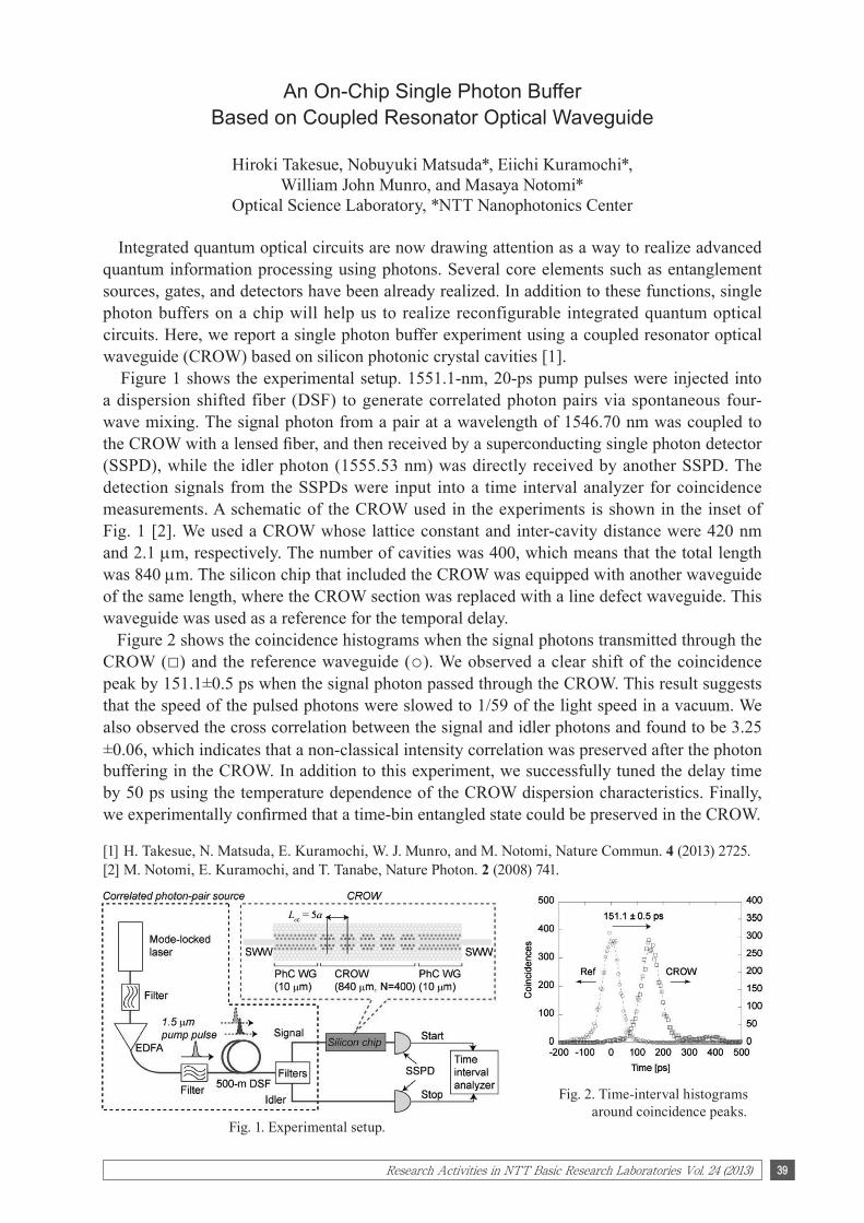
39Research Activities in NTT Basic Research Laboratories Vol. 24 (2013)
Fig. 1. Experimental setup.
Fig. 2. Time-interval histograms around coincidence peaks.
An On-Chip Single Photon Buffer Based on Coupled Resonator Optical Waveguide
Hiroki Takesue, Nobuyuki Matsuda*, Eiichi Kuramochi*, William John Munro, and Masaya Notomi*
Optical Science Laboratory, *NTT Nanophotonics Center
Integrated quantum optical circuits are now drawing attention as a way to realize advanced quantum information processing using photons. Several core elements such as entanglement sources, gates, and detectors have been already realized. In addition to these functions, single photon buffers on a chip will help us to realize reconfigurable integrated quantum optical circuits. Here, we report a single photon buffer experiment using a coupled resonator optical waveguide (CROW) based on silicon photonic crystal cavities [1]. Figure 1 shows the experimental setup. 1551.1-nm, 20-ps pump pulses were injected into a dispersion shifted fiber (DSF) to generate correlated photon pairs via spontaneous four-wave mixing. The signal photon from a pair at a wavelength of 1546.70 nm was coupled to the CROW with a lensed fiber, and then received by a superconducting single photon detector (SSPD), while the idler photon (1555.53 nm) was directly received by another SSPD. The detection signals from the SSPDs were input into a time interval analyzer for coincidence measurements. A schematic of the CROW used in the experiments is shown in the inset of Fig. 1 [2]. We used a CROW whose lattice constant and inter-cavity distance were 420 nm and 2.1 μm, respectively. The number of cavities was 400, which means that the total length was 840 μm. The silicon chip that included the CROW was equipped with another waveguide of the same length, where the CROW section was replaced with a line defect waveguide. This waveguide was used as a reference for the temporal delay. Figure 2 shows the coincidence histograms when the signal photons transmitted through the CROW (□) and the reference waveguide (○). We observed a clear shift of the coincidence peak by 151.1±0.5 ps when the signal photon passed through the CROW. This result suggests that the speed of the pulsed photons were slowed to 1/59 of the light speed in a vacuum. We also observed the cross correlation between the signal and idler photons and found to be 3.25 ±0.06, which indicates that a non-classical intensity correlation was preserved after the photon buffering in the CROW. In addition to this experiment, we successfully tuned the delay time by 50 ps using the temperature dependence of the CROW dispersion characteristics. Finally, we experimentally confirmed that a time-bin entangled state could be preserved in the CROW.
[1] H. Takesue, N. Matsuda, E. Kuramochi, W. J. Munro, and M. Notomi, Nature Commun. 4 (2013) 2725.[2] M. Notomi, E. Kuramochi, and T. Tanabe, Nature Photon. 2 (2008) 741.

40 Research Activities in NTT Basic Research Laboratories Vol. 24 (2013)
Fig. 1. Experimental configuration, (a) Setup of 90-km optical link and (b) Setup of DPS-QKD system.
Fig. 2. Experimental (a) QBER and (b) secure key generation rate for 25 days / 1 hour average.
Long-Term Performance of Quantum Key Distribution over 90-km Optical Links Installed in a Field Environment of Tokyo Metropolitan Area
Kaoru Shimizu, Kiyoshi Tamaki, and Toshimori Honjo*Optical Science Laboratory, *NTT Secure Platform Laboratories
The long-term operation performance, robustness and feasibility, of a differential phase shift (DPS) quantum key distribution (QKD) system to provide a long-distance key distribution service over optical fiber networks was examined by a series of field experiments that were carried out using a test-bed optical network in the Tokyo metropolitan area: Tokyo QKD network (Fig. 1) [1]. In spite of a 30-dB transmission loss and 90-km propagation along an optical link installed in a field environment, the stable generation of a secure key was demonstrated for 25 days in a completely free-run operation with a 1-GHz clock DPS-QKD system employing a weak coherent light pulse and superconducting single photon detectors (SSPDs) [2]. The average sifted key generation rate and the quantum bit error rate (QBER) were 11 kbps and 2.6 % (Fig. 2(a)), respectively. The average generation rate of secure key after error correction and privacy amplification was 1.1 kbps with a fluctuation of ±0.5 kbps (Fig. 2(b)). Here, we defined the secure key as the final key which was proven to be secure against general individual attacks. A comparison with meteorological data revealed the way in which the field environment influenced the key distribution performance. The secure key generation was considerably stable unless a strong wind disturbed the optical link which was composed of both aerial and underground regions with the approximately same total length. With the current system, some imperfections in photonic devices still limited the achievable performance levels, for example, the temporal bit error deterioration and the finite operation period. Some technical solutions were also provided to cope with these remaining problems. This work was carried out in fruitful collaboration with the National Institute of Information and Communications Technology (NICT).
[1] M. Sasaki et.al., Opt. Express 19 (2011) 10387.[2] K. Shimizu, T. Honjo, M. Fujiwara, T. Ito, K. Tamaki, S. Miki, T. Yamashita, H. Terai, Z. Wang, and M.
Sasaki, J. Lightwave Technol. 32 (2014) 141.

41Research Activities in NTT Basic Research Laboratories Vol. 24 (2013)
Fig. 1. Bright-field (BF) TEM image for a InP NW and a ball on graphene/SiC(0001).
Fig. 2. SEM images and panchromatic CL image for InP NWs on a micron Fe wire covered by graphene. The lower images were obtained at 14 K.
Growth of InP Nanowires on Graphene-Covered Fe
Kouta Tateno, Guoqiang Zhang, and Hideki GotohOptical Science Laboratory
Recently, the large-scale growth of single-layer and few-layer graphene has been demonstrated by the roll-to-roll fabrication method, and the advanced technique of transferring graphene sheets to flexible plastic substrates has led to stretchable, foldable, and transparent electronics and optoelectronics [1]. Graphene layers can be formed on many kinds of substrates. Here, we report on InP nanowires (NWs) on graphene/SiC(0001) and graphene-covered Fe. The vapor-liquid-solid (VLS) method is widely used to make freestanding NWs. The growth is driven catalytically in a nano-area by nanometer-scale metal particles. This feature is very useful for fabricating nanodevices because of the feasibility of forming p-n junctions and various heterostructures like quantum dots and core-shell structures. The VLS growth was carried out in a low-pressure metalorganic vapor phase epitaxy (MOVPE) reactor [2]. Trimethyl indium (TMIn) was the group-III source, and tertiarybutylphosphine (TBP) was the group-V source. We used Au particles as catalysts. The structures were observed by scanning electron microscopy (SEM) and transmission electron microscopy (TEM). III-V NWs tend to grow in the [111]B direction. Figure 1 shows a InP NW and an In ball grown on graphene/SiC(0001). Vertical NWs indicate that the (111)B face was likely to form initially on the 2D graphene surface. However, the low decomposition rate of TBP caused some In balls on the graphene surface. Some Au particles where the phosphorous supply was not enough could not form crystalline InP. This is due to less active sites on graphene to decompose TBP and also weak bonding characteristics of graphene surface. We have also tried to grow InP NWs on graphene/metal for flexible device application. After searching for proper metal among Cu, Ni and Fe, we could grow the NWs only on graphene/Fe. For Cu and Ni, the phosphorous reaction was so strong that it changed the surface morphology, which made the NW growth impossible. Fe forms various alloy compounds with carbon, and by adding carbon, Fe becomes harder, which is known as steel. The formation of steel would be important for the success of the subsequent InP NW growth. Figure 2 shows the demonstrated InP NWs grown on a micron Fe wire like spines of cacti. We also confirmed the cathodoluminescence (CL) from InP NWs. This system is very promising for a future NW application using flexible substrates.
[1] S. Bae et al., Nature Nanotech. 5 (2010) 574.[2] K. Tateno et al., Jpn. J. Appl. Phys. 53 (2014) 015504.

42 Research Activities in NTT Basic Research Laboratories Vol. 24 (2013)
Fig. 1. (Left) Process exciting a topological D band in a nanohorn. (Right) A path with a zero winding number does not contribute to the D band.
Topological Raman Band in the Carbon Nanohorn
Ken-ichi Sasaki, Yoshiaki Sekine*, Kouta Tateno, and Hideki GotohOptical Science Laboratory, *Materials Science Laboratory
Five-membered rings (pentagons) are found throughout the honeycomb network of carbon. For example, pentagons appear in fullerenes, at the apexes of carbon nanohorns, at the junctions of carbon nanotubes, and in a flat sheet of graphene as a constituent of the Stone-Wales defect [1]. A pentagon is a topological defect, which is represented as the flux of a pseudomagnetic field that is perpendicular with respect to the graphene layer [2]. An interesting consequence of such a flux in quantum mechanics is the Aharonov-Bohm (AB) effect. However, the AB effect is usually observed at very low temperature and/or for samples essentially devoid of defects so that they maintain coherence, which prevents us from utilizing the AB effect in practical applications. We show that a topological defect causes a special band (peak) in the Raman spectrum of a carbon nanohorn, which we call a topological Raman band [3]. A topological Raman band is excited through the AB effect for pentagons, and can be observed even at room temperature. A photo-excited "relativistic" carrier with a non-zero winding number is the key to activating a topological D Raman band (Fig. 1). A topological D band can be distinguished from the conventional D band excited at the graphene edge by its non-dispersive nature, because the selection rules for electron-phonon matrix elements are altered in an essential way by the presence of the pentagon.
[1] H. W. Kroto et al., Nature 318 (1985) 162; S. Iijima et al., Nature 356 (1992) 776; S. Iijima et al., Chem. Phys. Lett. 309 (1999) 165; A. Hashimoto et al., Nature 430 (2004) 870.
[2] J. González et al., Phys. Rev. Lett., 69 (1992) 172; P. E. Lammert et al., Phys. Rev. Lett., 85 (2000) 5190; K. Sasaki et al., Prog. Theor. Phys. 113 (2005) 463.
[3] K. Sasaki et al., Phys. Rev. Lett., 111 (2013) 116801.

43Research Activities in NTT Basic Research Laboratories Vol. 24 (2013)
Fig. 1. Spectral distribution of attosecond pulse with (a) carbon filter and (b) carbon and boron filters.
Fig. 2. Fourier-transform-limited pulse.
Generation of Isolated Attosecond Pulse in Carbon K-Edge (284 eV) Region with Double Optical Gating
Hiroki Mashiko, Tomohiko Yamaguchi, Katsuya Oguri, and Hideki GotohOptical Science Laboratory
As is well known, carbon is important fundamental element of inorganic compounds (graphene, nanotube, etc.) and organic compounds (hydrocarbon, bio cell, etc.). The K-shell absorption edge in carbon [284 eV photon energy (4.4 nm wavelength)] has capability for optical imaging the element. Meanwhile, attosecond (10–18 s: as) pulse is shortest laser pulse in the world. The laser with ultrashort pulse width would be useful for visualizing of living cell structure. In order to generate the attosecond pulse with 284 eV photon energy, the peak intensity of the driving laser should be >1.4×10¹⁵ W/cm2 [1]. Here, we report attosecond pulse generation with only 247 μJ pulse energy using a double optical gating (DOG) [2]. The technique is combined with elliptically dependent polarization gating and two-color gating. The temporal gate effect can emphasize the cut-off spectrum component in the pulse. In this experiment, we used the Ti:Sapphire laser with 247 μJ pulse energy with 7 fs duration. The temporal gate width with DOG was fixed to ~1.3 fs. The driving laser was focused on a cell filled with helium gas (backing pressure: ~1.2 bar, interaction length: 300 μm). The spectrum of generated attosecond pulse was monitored with a soft x-ray spectrometer (resolution: 3.8 eV in the 284 eV region). Figure 1 shows the spectral distribution with (a) the carbon filter and (b) carbon and boron filters. The boron K-edge (188 eV) and carbon K-edge (284 eV) were clearly observed. Consequently, 284 eV pulse were successfully generated from the driving laser with only 247 μJ pulse energy, which pulse energy is lowest value ever reported. In addition, the spectral bandwidth is larger than 140 eV. The Fourier-transform-limited pulse, assuming a flat phase, was 20 as duration as shown in Fig. 2. The value is much shorter than previous reported value of 80 as in the world record [3]. The characteristic time scale for electron motion is atomic unit of time, which is 24 as. The attosecond pulse will have a profound impact on the study of various electron dynamics in the carbon K-edge region.
[1] Z. Chang et al., Phys. Rev. Lett. 79 (1997) 2967.[2] H. Mashiko et al., Appl. Phys. Lett. 102 (2013) 171111.[3] E. Goulielmakis et al., Science 320 (2008) 1614.

44 Research Activities in NTT Basic Research Laboratories Vol. 24 (2013)
Fig. 1. GaAs quantum dots (QD) and experimental configuration around QD sample.
Fig. 2. Laser metal power dependence of photoluminescence spectra for QD.
Modification of Exciton Optical Properties with Coherent Phonons inQuantum Dots
Hideki Gotoh, Haruki Sanada, Hiroshi Yamaguchi*, and Tetsuomi SogawaOptical Science Laboratory, *Physical Science Laboratory
Optically active semiconductor quantum dots (QDs) have been extensively studied because they are good candidates for quantum devices. Quantum devices rely on the optical properties of the excitons in QDs, which exist more stably than in other semiconductors. Excitons should be coherently manipulated without any decoherence processes for quantum device applications. Previously, optical, electric, and magnetic fields have been employed as sources for the manipulation. In this report, we show that coherent phonons induced by ultrafast optical pulses will provide a good new approach to QD manipulation [1]. The QD sample used in the measurement was based on GaAs/AlGaAs quantum wells (QWs) fabricated on an undoped (001) GaAs substrate. The QDs were formed in a thin (4.2 nm thick) GaAs layer sandwiched between AlGaAs barriers. The QD sample had a 100 nm-thick titanium film on its surface and the QDs were located 100 nm below the surface. In the measurement, we used a pulse laser (duration: 150 fs, repetition: 80 MHz, energy: 1.653 eV) as the excitation source. Optical pulses from the source were divided into two paths: one (Laser PL) was for creating excitons in QDs and the other (Laser Metal) was for illuminating the metal film as in Fig. 1. Figure 2 shows the PL spectra for different laser metal intensities with the laser PL power constant. Fine well-separated PL peaks were seen in the PL spectrum for laser PL (Laser Metal = 0 mW). The PL peaks originated from single excitons confined in the QDs. The spectra changed greatly with increases in Laser Metal intensity. These phenomena cannot be explained simply in terms of the heating effects induced by the laser metal. As an alternative way of evaluating the effects of illuminating metal, we also measured the reflectance properties using an optical interferometric method. Clear time-oscillating interferometric signals were observed that responded to the intensity of Laser Metal. The oscillating signals confirmed that coherent phonons were created in the QD sample. In QDs, coherent phonons form time- and space-oscillating strain waves leading to a change in the PL properties. The coherent phonons will constitute a new manipulation source whose response time is much shorter than that of previous methods employing ultrafast optical sources.
[1] H. Gotoh, H. Sanada, H. Yamaguchi, and T. Sogawa, Appl. Phys. Lett. 103 (2013) 112104.

45Research Activities in NTT Basic Research Laboratories Vol. 24 (2013)
Optical Nanocavity Formed by a Semiconductor Nanowire and a Si Photonic Crystal
Atsushi Yokoo1,2, Muhammad Danang Birowosuto1,2, Guoquiang Zhang2, Kouta Tateno2, Masato Takiguchi1,2, Eiichi Kuramochi1,2, Hideaki Taniyama1,2, Masaya Notomi1,2
1NTT Nanophotonics Center, 2Optical Science Laboratory
Semiconductor nanowires are attractive for their small diameters of less than 100 nm. In particular, III-V semiconductor nanowires can be used in a variety of structures, such as core-shell and multilayer heterostructures and p-i-n junctions, by arranging growth sequences in epitaxial growth, which may enable us to realize small optical devices with low energy consumption. However, a nanowire itself can not provide sufficient optical confinement to achieve the desired device performance because it is too small to match the wavelength of light. On the other hand, Si photonic crystal provides optical confinement with the dimension of the wavelength of light; however, it requires a regrowth process in order to incorporate optically active material. Therefore, the types of materials we can use with Si photonic crystal are limited. Here, we demonstrate that a nanocavity can be created in a photonic crystal by placing a nanowire in a trench in a line defect of Si photonic crystal. We move the nanowire by means of AFM manipulation, in which a nanoprobe can be used to drag a small object. In addition, the position of the nanocavity can be shifted by moving the nanowire in the trench (Fig. 1) [1]. The nanocavity is a mode-gap cavity generated by partially changing the effective refractive index in the line defect [2, 3]. We obtained the highest Q-factor of 9500 (resonant wavelength: 1.5 μm) for a sample with a InAsP/InP heterostructure nanowire (2620-nm length, 85-nm diameter) installed into a trench in a line defect (lattice constant of 416 nm, trench width of 150 nm, depth of 75 nm) of a photonic crystal. As the the Q-factor for the movable cavity can vary at each nanowire position, we can evaluate the Q-factor dependence of cavity photon lifetime by evaluating each photon lifetime in the nanowire-induced cavities with an identical nanowire placed at different positions. We confirmed that the photon lifetime decreases with increasing Q-factor, which can be attributed to the Purcell effect. We obtained a photon lifetime of 91 ps for a nanowire-induced photonic crystal cavity with a Q-factor of 5200, which is the shortest lifetime ever achieved for a III-V semiconductor nanowire. This demonstration indicates the possibility of realizing photonic integrated circuits on demand, where optically active material is installed into a universal photonic crystal substrate to provide a nanocavity with the desired functionality.
[1] M. D. Birowosuto, A. Yokoo, G. Zhang, K. Tateno, E. Kuramochi, H. Taniyama, M. Takiguchi, and M. Notomi, Nature Mater. 13 (2014) 279.
[2] M. Notomi and H. Taniyama, Optics Express 16 (2008) 18657.
[3] M. D. Birowosuto, A. Yokoo, H. Taniyama, E. Kuramochi, M. Takiguchi, and M. Notomi, J. Appl. Phys. 112 (2012) 113106.
Fig. 1. Diagram of cavity creation by installing a nanowire into a trench in a line defect of photonic crystal by AFM manipulation. The nanowire is moved in the trench to realize a movable cavity. Spectra show an emission from the nanowire-induced cavity located at different positions.

46 Research Activities in NTT Basic Research Laboratories Vol. 24 (2013)
Fig. 1. Device structure (a) Schematic of PhC-based pin-PD. (b) SEM image of fabricated sample.
Fig. 2. Device characteristics (a) Photocurrent versus optical input power characteristics. (b) Eye pattern for 10 Gb/s optical signal.
InGaAs Photodetectors Based on Photonic Crystal Waveguide Including Ultrasmall Buried Heterostructure
Kengo Nozaki, Shinji Matsuo*, Koji Takeda*, Tomonari Sato*, Eiichi Kuramochi,and Masaya Notomi
Optical Science Laboratory, *NTT Photonics Laboratories
Low-power optical link between CMOS chips and photonic network on chip have been extensively studied. One of the challenges with photodetectors (PDs) is to realize a small junction capacitance to use as a receiver in such short-range optical links. If the capacitance can be greatly reduced by reducing the size of the PDs, the RC constant could be kept at a low level even during connection with a high load resistor. The result would be a low thermal noise and an enhanced output voltage while maintaining a fast response. This would lead to the reduction of electrical amplification or even its elimination (referred as a receiver-less PD). There would then be a strong demand for nano-PDs with a small junction capacitance and high absorption efficiency. Semiconductor photonic crystal (PhC) can confine light in a small core waveguide, which means that high responsivity can still be expected for a few-μm-long PD. This also enables us to reduce the length of the p-i-n junction and subsequently reduce the junction capacitance. Figure 1 is a schematic and SEM image of our PD based on a PhC waveguide [1]. An InGaAs bulk absorption layer with a length of only 3.4 μm was embedded in the waveguide, and Zn and Si ion were doped to form the lateral p-i-n junction. The photocurrent for input of CW light is shown in Fig. 2(a). We estimated a sufficiently large responsivity of ~1 A/W at a bias voltage of –1 V. This means that there was no apparent non-radiative recombination or carrier trapping at the hetero interface, which is unique and significant for our BH structure. Figure 2(b) shows an eye pattern for modulated light with 231–1 pseudo-random bit sequence, indicating a good response for a bit rate of 10 Gb/s. We can expect faster response speed by reduction of RC time constant, and the on-chip light-to-voltage conversion would be possible if the PD is connected with load resistance. They would make us to expect a great potential for use as an integrable low-power photoreceivers in future intra-chip optical networks.
[1] K. Nozaki, S. Matsuo, K. Takeda, T. Sato, E. Kuramochi, and M. Notomi, Opt. Express 21 (2013) 19022.

47Research Activities in NTT Basic Research Laboratories Vol. 24 (2013)
Fig. 1. (a) Schematic of L2 PhC cavity structure. An active region is embedded inside an L2 photonic crystal cavity. (b) Cross-section of BH-QW-PhC structure.
Fig. 2. (a). Emission lifetimes from L2 cavity on-resonant, L2 cavity off-resonant and BH-QW without PhC (0.80×0.30×0.15 μm3). (b) L2 cavity spectrum at 4 K.
Enhanced and Suppressed Spontaneous Emission from a Buried Heterostructure Photonic Crystal Cavity
Masato Takiguchi1,2, Hisashi Sumikura1,2, Muhammad Danang Birowosuto1,2, Eiichi Kuramochi1,2, Tomonari Sato1,3, Koji Takeda1,3, Shinji Matsuo1,3, and Masaya Notomi1,2
1NTT Nanophotonics Center, 2Optical Science Laboratory, 3NTT Photonics Laboratories
Chip-scale optical interconnection and photonic network-on-chip architecture are being widely studied. Among various candidates, a photonic crystal (PhC) cavity device is promising because its ultra-small mode volume and high quality factor (Q) will enable high-speed modulation devices, such as lasers and light emitting diodes (LEDs). To realize efficient and ultrafast light-emitting nanophotonic devices, we study spontaneous emission control in a buried-heterostructure (BH) photonic crystal cavity in which InGaAsP quantum wells (QW) are embedded in an InP PhC (Fig. 1). Spontaneous emission from conventional QW-PhC cavities have been extensively investigated, but they suffer from poor carrier confinement and surface non-radiative recombination. Therefore, the spontaneous emission control has been only observed in quantum dots PhC cavities. The present study shows that BH-QW-PhC cavities can exhibit distinctive spontaneous emission control in QW-PhCs because of strong carrier confinement and low surface non-radiative recombination. In this experiment [1], we examined the emission enhancement and suppression in our samples with different lattice constants at 4K. Figure 2(a) shows the PL decay for the L2 cavity at 1406 nm in an off-resonant condition, at 1430 nm in an on-resonant condition and a reference QW emission, measured at excitation powers of 100 nW, which is 10 times lower than the lasing threshold. Here we used the L2 cavity with a quality factor of 4200 (Fig. 2 (b)). As seen in Fig. 2(a), the on-resonant emission apparently becomes faster, and the emission rate obtained by a single exponential fitting was 4.9×10⁹ s–1 (tPL = 0.2 ns) which is 3.8 times faster than the same-size BH-QW without the PhC structure. The off-resonant emission rate was 1.7×10⁸ s–1 (tPL = 6.0 ns) and 7.5 times slower than the BH-QW emission without a PhC structure. This means that we can control the spontaneous emission rate by a factor of 30 between on-resonant and off-resonant conditions. This is the largest ratio observed in QW-PhCs, and comparable to the best QD-PhCs. The result implies our devices may have high spontaneous emission coupling efficiency, BH-QW-PhC cavities should be promising for devices light emitting based on cavity QED effects, and that they have great potential for realizing very efficient and ultra-fast light-emitting nanophotonic devices.
[1] M. Takiguchi, H. Sumikura, M. D. Birowosuto, E. Kuramochi, T. Sato, K. Takeda, S. Matsuo, and M. Notomi, Appl. Phys. Lett. 103 (2013) 091113.
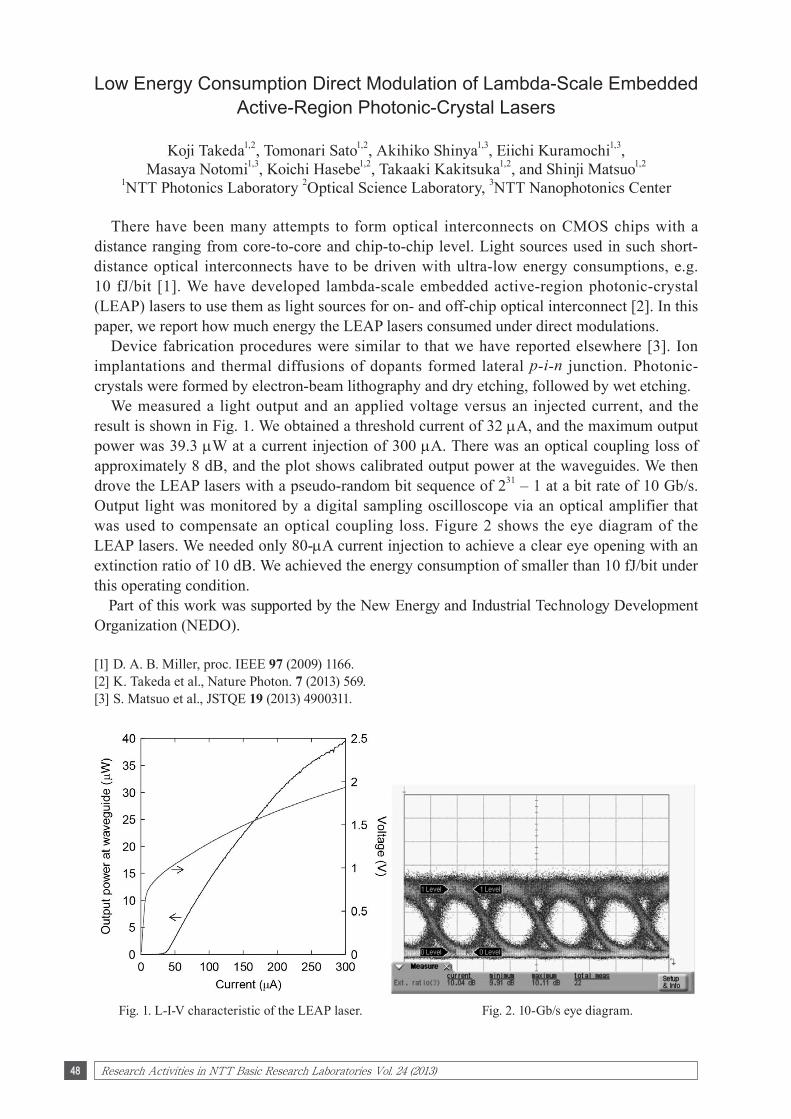
48 Research Activities in NTT Basic Research Laboratories Vol. 24 (2013)
Fig. 1. L-I-V characteristic of the LEAP laser. Fig. 2. 10-Gb/s eye diagram.
Low Energy Consumption Direct Modulation of Lambda-Scale Embedded Active-Region Photonic-Crystal Lasers
Koji Takeda1,2, Tomonari Sato1,2, Akihiko Shinya1,3, Eiichi Kuramochi1,3, Masaya Notomi1,3, Koichi Hasebe1,2, Takaaki Kakitsuka1,2, and Shinji Matsuo1,2
1NTT Photonics Laboratory 2Optical Science Laboratory, 3NTT Nanophotonics Center
There have been many attempts to form optical interconnects on CMOS chips with a distance ranging from core-to-core and chip-to-chip level. Light sources used in such short-distance optical interconnects have to be driven with ultra-low energy consumptions, e.g. 10 fJ/bit [1]. We have developed lambda-scale embedded active-region photonic-crystal (LEAP) lasers to use them as light sources for on- and off-chip optical interconnect [2]. In this paper, we report how much energy the LEAP lasers consumed under direct modulations. Device fabrication procedures were similar to that we have reported elsewhere [3]. Ion implantations and thermal diffusions of dopants formed lateral p-i-n junction. Photonic-crystals were formed by electron-beam lithography and dry etching, followed by wet etching. We measured a light output and an applied voltage versus an injected current, and the result is shown in Fig. 1. We obtained a threshold current of 32 μA, and the maximum output power was 39.3 μW at a current injection of 300 μA. There was an optical coupling loss of approximately 8 dB, and the plot shows calibrated output power at the waveguides. We then drove the LEAP lasers with a pseudo-random bit sequence of 231 – 1 at a bit rate of 10 Gb/s. Output light was monitored by a digital sampling oscilloscope via an optical amplifier that was used to compensate an optical coupling loss. Figure 2 shows the eye diagram of the LEAP lasers. We needed only 80-μA current injection to achieve a clear eye opening with an extinction ratio of 10 dB. We achieved the energy consumption of smaller than 10 fJ/bit under this operating condition. Part of this work was supported by the New Energy and Industrial Technology Development Organization (NEDO).
[1] D. A. B. Miller, proc. IEEE 97 (2009) 1166.[2] K. Takeda et al., Nature Photon. 7 (2013) 569.[3] S. Matsuo et al., JSTQE 19 (2013) 4900311.

49Research Activities in NTT Basic Research Laboratories Vol. 24 (2013)
Fig. 1. The responsivity of the GePD for various bias voltages.
Fig. 2. Normalized responsivity of the GePD for various bias voltages.
Fig. 3. The minimum detection limit of GePD at a wavelength of 1640 nm.
Significant L-Band Responsivity Improvement of Germanium Waveguide Photodiode by Franz-Keldysh Effect
Kotaro Takeda, Tatsurou Hiraki, Tai Tsuchizawa, Hidetaka Nishi, Rai Kou, Hiroshi Fukuda1, Tsuyoshi Yamamoto1, Yasuhiko Ishikawa2, Kazumi Wada2, and Koji Yamada
NTT Nanophotonics center, 1NTT Microsystem Integration Laboratories, 2The University of Tokyo
The responsivity of germanium photodiode (GePD) for L-band (1565 – 1625 nm) decreases because of a decrease in the absorption coefficient of germanium around 1580-nm wavelength [1]. Hence, increase in the responsivity is required to apply a GePD as a photodetector for the L-band. Under a high-bias condition, the Franz-Keldysh (FK) effect might increase responsivity in the L-band. An increase of absorption coefficients under high bias voltage was recently observed in the band around 1580 nm [2]. Moreover, the avalanche effect also might increase responsivity in the L-band. The avalanche multiplication gain should be observed in the L-band because it does not depend on wavelength. In this study, we investigate the responsivity of a GePD driven with a high bias field to give rise to the FK and avalanche effects in the L-band. And we separate the contribution of each to the responsivity by calculating the influences of them. We employed a waveguide coupled GePD to measure the responsivity in the L-band under high bias voltage. The width, length, and thickness of the Ge mesa are 10, 50, and 1 μm, respectively. The dark currents are about 117 nA and 111 μA at 2- and 15-V bias voltage. Figure 1 shows the responsivity of the GePD for various bias voltages. The responsivity at 15 V bias reaches over 1.14 A/W in the whole L-band. At bias voltage above 11 V, it increases with bias voltage owing to the avalanche effect. In order to exclude the influence of avalanche effect, the responsivity was normalized by the avalanche multiplication factor (Mav) as shown in Fig. 2. In the band from 1550 to 1640 nm, the responsivity increases for all bias voltages. This behavior agrees well with the calculation result of FK effect described as solid line in Fig. 2. Thus, we conclude that the high responsivity in the L-band of GePD is derived from the FK and the avalanche effect. Figure 3 (a) shows the minimum detection limit of GePD at a wavelength of 1640 nm. The minimum detection limits decrease because of the responsivity increase due to the FK effect as the bias voltage increases. However, they increase rapidly at bias voltage of over 11 V. This is because huge noise from dark current due to avalanche multiplication. Figure 3 (b) shows the minimum detection limit when the dark current is suppressed to 1/50 of the experimental values in this work. The avalanche effect is effective in this case. Thus, Optimized reduction of dark current and control of the bias field applied to Ge are necessary to obtain effective multiplication due to both effects. To the best of our knowledge, this study is the first observation of responsivity increase in GePD for the L-band. And it opens up a possibility of GePD as L-band detector. [1] C. T. DeRose, et al., Opt. Express 19 (2011) 24897.[2] T. Y. Liow, et al., in Proc. OFC, no OM3K. 2 (2013).


Ⅱ.Data

51Research Activities in NTT Basic Research Laboratories Vol. 24 (2013)
6th NTT-BRL School
The sixth NTT Basic Research Laboratories (BRL) School was held on November 24-26, 2013 at our NTT Atsugi R&D Center. The aim of the school was to foster young researchers in the nano and quantum science fields and to promote the international visibility of NTT BRL. This year the theme of the school was "Nano and Quantum Science: Driving Tomorrow’s Technology", closely related to ongoing research within NTT BRL. Prestigious professors and researchers were invited as the school lecturers. We accepted thirty-five students, mainly Ph. D students, from fourteen countries. On the first day, Prof. John Clarke (University of California, Berkeley, U.S.A.) presented lectures entitled "Theory, practice and applications of Superconducting Quantum Interference Devices (SQUIDs)". He also gave lectures on the second day that covered applications ranging from cosmology to medicine using SQUID femtoscience. On the afternoon of the first day, after the director of NTT BRL, Dr. Tetsuomi Sogawa, provided an introduction of NTT Laboratories, while the three senior distinguished researchers of NTT BRL gave lectures on "Micro/nanomechanical systems using compound semiconductor heterostructures" by Dr. Hiroshi Yamaguchi, "Topologically protected quantum effects in solid state" by Dr. Koji Muraki, and "Nanophotonics toward the smallest energy consumption" by Dr. Masaya Notomi. On the second and third day, Prof. Oliver Schmidt (Institute Director, IFW Dresden, Germany) gave two lectures entitled "Quantum dots: From growth to quantum device" and "Shaping nanomembranes into a new nanoworld". After the lecture of the second day, we conducted a lab tour to show our research facilities and introduce recent research activities at NTT BRL. Then we went on an excursion to Mt. Ohyama belonging to Tanzawa mountain range which is close to the NTT Atsugi R&D Center. The participants enjoyed foliage that was lighting up and tofu dishes at a Japanese traditional restaurant. On the third day, Prof. Jonathan Finley (Walter Schottky Institute, Germany) gave a lecture on "Optically probing charge and spin dynamics in single and coupled quantum dots". After the lecture, all participants attended ISNTT (an international conference on nanoscale transport and technology) hosted by NTT BRL. As part of this, the students gave poster presentations regarding their university research. All students, lecturers, and NTT BRL researchers had excellent time exchanging information on current research topics in various fields. In the joint party of BRL School and ISNTT, "Best Poster Prizes" were awarded to three students who gave noteworthy poster presentations. The students got the opportunity to discuss high-quality research and build human network and friendships within this school. NTT BRL will continue to provide these occasions to support young researchers and to establish research collaborations in the fields of nano and quantum science.

52 Research Activities in NTT Basic Research Laboratories Vol. 24 (2013)
International Symposium on Nanoscale Transport and Technology (ISNTT2013)
International Symposium on Nanoscale Transport and Technology (ISNTT2013) was held at the NTT Atsugi R&D Center from November 26 to 29, 2013, and brought together 208 participants from 16 countries. The participants enjoyed oral and poster presentations at the symposium, exchanging their views and ideas on nanotechnology and quantum devices. Since 1998, NTT Basic Research Laboratories (BRL) has been holding a lot of international conferences on various topics and technologies. ISNTT was first organized in 2009 to promote mutual exchange between different device and material technologies on semiconductors, superconductors, and new materials, and since then it has been held about every two years. ISNTT2013 of which the logo represents hybrid system was co-chaired by Drs. Akira Fujiwara, Hiroshi Yamaguchi, and Koji Muraki of NTT BRL, and it was aimed at further enhancing interaction among different research fields to develop new idea and technology. On the 26th, 27th, and 29th, respectively, the session started with keynote lectures entitled "The UC Santa Barbara quantum computing effort" by Prof. Andrew Cleland (University of California), "Quantum anomalous Hall effect in magnetic topological insulators" by Prof. Qi-Kun Xue (Tsinghua University), and Flying qubits and quantum electron optics with surface acoustic wave by Prof. Seigo Tarucha (The University of Tokyo). Throughout the symposium we had 13 oral sessions with 48 oral presentations including 17 invited talks by world leading researchers, on nanodevices, topological insulators, nanomechanics, quantum bits and computers, single-electron devices, graphene, quantum spin Hall effect, optical devices, and so on. In addition there were 71 presentations at the poster session on the 26th and 27th. Since a part of the poster sessions was held jointly with the 6th NTT-BRL school, many young researchers and students had enthusiastic discussions in front of the posters. The symposium was stimulating and successful, strengthening worldwide network among researchers based on the open-laboratory policy of NTT BRL.

53Research Activities in NTT Basic Research Laboratories Vol. 24 (2013)
List of BRL Seminars (Fiscal 2013)
Date Speaker AffiliationTitle
May-10 Dr. Rin OkuyamaKeio University, JapanLasing of optical phonons in semiconductor double quantum dots
May-21 Prof. Andrea Fiore Eindhoven University of Technology, the NetherlandsTowards fully integrated quantum photonic circuits
May-24 Mr. Kiyoshi KanazawaKyoto University, JapanEnergy transport driven by a thermal non-Gaussian fluctuations
Jun-12 Prof. Mark SanquerCEA-INAC-SPSMS, FranceThe coupled atom transistor: a first realization with shallow donors implanted in a trigate silicon nanowire
Jun-19 Prof. Nobuhisa Ishii
The University of Tokyo, JapanGeneration of few-cycle, intense IR pulses from a BIBO-based optical parametric chirped pulse amplifier and their use in the generation of waveform-dependent high harmonics in the water window
Jul-5 Dr. Alex S. ClarkUniversity of Sydney, AustraliaNonlinear quantum photonics: generating and manipulating single photons
Jul-10 Prof. Marko LoncarHarvard University, U.S.A.Group IV Photonics: From Silicon to Diamond "Si optomechanics and Diamond nanophotonics"
Jul-11 Mr. Takuro IdeguchiMr. Simon Holzner
Max-Planck-Institute of Quantum Optics, GermanyAdaptive dual-comb spectroscopy
Sep-3 Dr. Michael Jack Scion, New ZealandFrom cold atoms to warm molecules
Sep-6 Akira Saito Ph. D.National Institute of Informatics (NII), JapanImpracticality of coherent computing and annealing machine models
Sep-11 Prof. Igor Aharonovich University of Technology, Sydney (UTS), AustraliaWide bandgap semiconductors for Nanophotonics
Sep-11Prof. Benoit HackensDr. Sébastien FanielDr. Frederico Martins
Université catholique de Louvain, BelgiumImaging and manipulating quantum transport at the nanometer scale

54 Research Activities in NTT Basic Research Laboratories Vol. 24 (2013)
Date Speaker AffiliationTitle
Sep-13 Dr. Hari Dahal American Physical Society, U.S.A.APS publications and peer-review in PRB
Sep-26 Dr. Shota KitaHarvard University, U.S.A.Optomechanical Nanobeam Transducers towards Ultrahigh Resolution Mass Spectrometry
Oct-24 Prof. Hiroyuki Hirayama Tokyo Institute of Technology, JapanSilicene formed by epitaxial growth
Oct-31 Prof. Gerard J. Milburn The University of Queensland, AustraliaSingle photon opto-mechanics
Nov-5 Prof. Peide Ye Purdue University, U.S.A.2D Materials and Devices beyond Graphene
Nov-5 Prof. Andrew WhiteThe University of Queensland, AustraliaIntriguing chemists and upsetting computer scientists using light and mirrors
Nov-7 Dr. Kenji Yoshii
Japan Atomic Energy Agency (JAEA) / Okayama University, JapanNovel multiferroic materials RFe2O4 (R: rare-earth element) –Their discovery and subsequent development
Nov-11 Dr. Nicolas Clément
CNRS, FranceEmergence of 0D Ion-Sensitive Field Effect Transistors -A new tool for energy harvesting and electrical study of single biomolecules ?-
Nov-13 Prof. Pawel Hawrylak
National Research Council of Canada, CanadaElectron-electron interactions, topology and transport and optical spin blockade in semiconductor and graphene quantum dots
Nov-21 Dr. Neill LambertRIKEN, JapanNon-equilibrium QED: from nano-mechanics to hybrid devices
Dec-5 Dr. Yasuhiro YamadaThe University of Tokyo, JapanResolution Effects on Current Measurement in Nanoscale Systems
Dec-10 Dr. Ed Gerstner Executive editor of Nature Communications, U.K.Nature open access journals seminar

55Research Activities in NTT Basic Research Laboratories Vol. 24 (2013)
Date Speaker AffiliationTitle
Dec-16 Dr. Kazuyuki NakayamaFukuoka University, JapanManipulation of Spontaneous Emission with Quasi-periodic Metamaterials
Dec-19 Dr. Gregor Koblmüller Technical University Munich, GermanyProgress in arsenide-based nanowires and their devices
Jan-16 Dr. Daryl BeggsThe University of Bristol, U.K.Optical delay in silicon photonic crystal waveguides: accelerating slow-light
Jan-23 Prof. Jing KongMassachusetts Institute of Technology, U.S.A.Synthesis and applications of graphene and related nanomaterials
Feb-5 Prof. Michael Trupke The Vienna University of Technology, AustriaDiamond defects for sensing and quantum applications
Feb-21 Dr. Kei SawadaRIKEN, JapanBerry-phase theory with analogy among optics, dynamics, and electric circuits
Mar-3 Prof. Isabelle Zaquine Telecom Paris Tech, FranceMulti-user entanglement distribution at telecom wavelength
Mar-10 Dr. Michael R. VannerThe University of Queensland, AustraliaExperimental non-linear optomechanical measurement of mechanical motion
Mar-12 Dr. Erwann Bocquillon Ecole Normale Supérieure, FranceElectron quantum optics in quantum Hall edge channels
Mar-26 Dr. Mandar DeshmukhTata Institute of Fundamental Research, IndiaProbing phase transitions in nanoscale correlated systems showing MIT and CDW physics using nanomechanics

56 Research Activities in NTT Basic Research Laboratories Vol. 24 (2013)
Award Winners’ List (Fiscal 2013)
The Commendation for Science and Technology by the Minister of Education, Culture, Sports, Science and Technology, Research Category Prize
H. YamaguchiOptoelectromechanical hybrid devices using compound semiconductor heterostructures
Apr. 16,2013
The Commendation for Science and Technology by the Minister of Education, Culture, Sports, Science and Technology, The Young Scientists’ Prize
K. Nishiguchi Nanometer-scale semiconductor devices with high functionality
Apr. 16,2013
JSAP Fellow H. Yamaguchi
Pioneering Contributions to the Application of Compound Semiconductor Heterostructures to Mechanical Devices
Sep. 16, 2013
JSAP Outstanding Paper Award
K. NishiguchiA. Fujiwara
Single-Electron Stochastic Resonance Using Si Nanowire Transistors
Sep. 16,2013
Human communication award M. Yamaguchi
A case study of the communication between families living at remote locationReport of the communication style using "Denwa-channel" for five years
Dec. 19,2013
6th International Symposium on Advanced Plasma Science and its Applications for Nitrides and Nanomaterials, Best Presentation Award
C.-H. LinN-face GaN (000-1) films grwon by group-III source flow-rate modulation epitaxy
Mar. 6,2014
JSAP Young Scientist Oral Presentation Award S. Tanabe Damage-free transfer of graphene
grown on SiCMar. 17,2014
JSAP Poster Awards
T. GotoA. IshizawaH. NishiN. MatsudaR. KouK. HitachiT. NishikawaK. YamadaT. SogawaH. Gotoh
On-chip supercontinuum generation from a dispersion-controlled silicon waveguide
Mar. 18,2014

57Research Activities in NTT Basic Research Laboratories Vol. 24 (2013)
In-house Award Winners’ List (Fiscal 2013)
NTT Science and Core Technology Laboratory Group Director Award
H. SanadaY. KunihashiK. OnomitsuH. Gotoh
Magnetic-field-free mobile spin resonance in high-purity semiconductor heterostructures
Dec. 20, 2013
BRL Director Award Award for Achievements
K. NishiguchiA. Fujiwara
New applications using silicon nanometer-scale devices at room temperature
Mar. 27, 2014
BRL Director Award Award for Achievements
A. YokooD. BirowosutoG. ZhangK. TatenoE. KuramochiM. TakiguchiM. Notomi
Inventive approach for integration of nanowire into nanophotonics by using nanomanipulation
Mar. 27, 2014
BRL Director Award Award for Excellent Papers
Y. KrockenbergerH. IrieO. MatsumotoK. YamagamiM. MitsuhashiA. TsukadaM. NaitoH. Yamamoto
"Emerging superconductivity hidden beneath charge-transfer insulators"Scientific Reports 3, 2235 (2013)
Mar. 27, 2014
BRL Director Award Award for Excellent Papers
I. MahboobK. NishiguchiA. FujiwaraH. Yamaguchi
"Phonon Lasing in an Electro- mechanical Resonator"Physical Review Letters 110, 127202 (2013)
Mar. 27, 2014
BRL Director Award Award for Excellent Papers
K. SasakiY. SekineK. TatenoH. Gotoh
"Topological Raman Band in the Carbon Nanohorn"Physical Review Letters 111, 116801 (2013)
Mar. 27, 2014
BRL Director Award Award for Performance
K. OnomitsuT. HayashiK. Suzuki
Contribution for significant enhancement in durability, safety, and cost reduction of liquid nitrogen supply system
Mar. 27, 2014
BRL Director Award Award for Encouragement D. Hatanaka
Novel structural mechanical systems using semiconductor based mechanical resonators
Mar. 27, 2014
BRL Director Award Award for Encouragement K. Hitachi Nonlinear optics for frequency
stabilized optical frequency combMar. 27, 2014
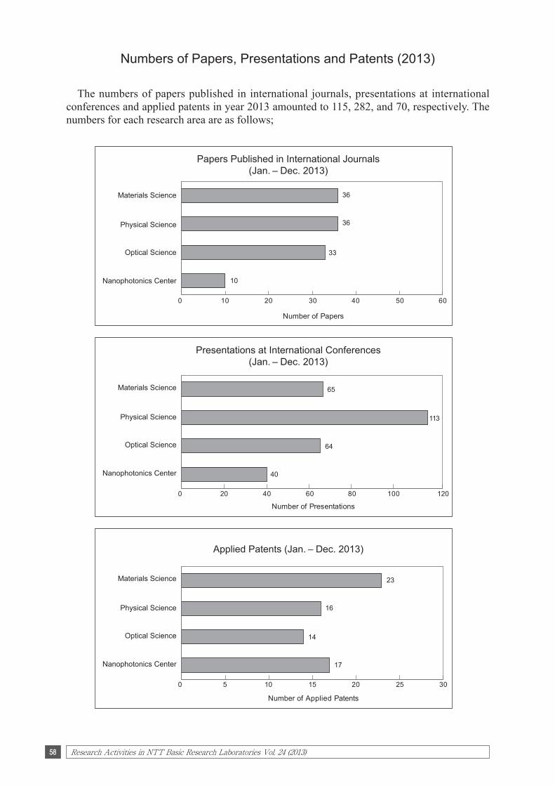
58 Research Activities in NTT Basic Research Laboratories Vol. 24 (2013)
Numbers of Papers, Presentations and Patents (2013)
The numbers of papers published in international journals, presentations at international conferences and applied patents in year 2013 amounted to 115, 282, and 70, respectively. The numbers for each research area are as follows;
0 20 40 60 80 100 120
0 10 20 30 40 50 60
0 5 10 15 20 25 30
10
33
36
36
40
64
65
113
17
14
23
16
Number of Papers
Number of Presentations
Number of Applied Patents
Papers Published in International Journals(Jan. – Dec. 2013)
Presentations at International Conferences(Jan. – Dec. 2013)
Applied Patents (Jan. – Dec. 2013)
Optical Science
Nanophotonics Center
Physical Science
Materials Science
Optical Science
Nanophotonics Center
Physical Science
Materials Science
Optical Science
Nanophotonics Center
Physical Science
Materials Science

59Research Activities in NTT Basic Research Laboratories Vol. 24 (2013)
The numbers of research papers published in the major journals are shown below.Journals (IF2012)* NumbersApplied Physics Letters 3.794 16
Physical Review B 3.767 16
Japanese Journal of Applied Physics 1.067 8
Optics Express 3.546 7
Applied Physics Express 2.731 6
Nature Communiation 10.015 5
Journal of Crystal Growth 1.552 5
Physical Review A 3.042 4
Physical Review Letters 7.943 3
New Journal of Physics 4.063 3
AIP Advances 1.349 3
Nature Physics 19.352 2
Scientific Reports 2.927 2
Journal of Applied Physics 2.21 2
Nature Nanotechnology 31.17 1
Nature Photonics 27.254 1
Reports on Progress in Physics 13.232 1
Nano Letters 13.025 1
ACS Nano 12.062 1
Nano Research 7.392 1
Chemical Communications 6.378 1
Journal of Physical Chemistry C 4.814 1
Journal of Biological Chemistry 4.651 1
Optics Letters 3.385 1
Ultramicroscopy 2.47 1*IF2012:Impact Factor 2012
The average IF2012 for all research papers from NTT Basic Research laboratories is 4.40.
The numbers of presentations in the major conferences are shown below.Conferences NumbersInternational Symposium on Nanoscale Transport and Technology 2013(ISNTT2013) 31
40th International Symposium on Compound Semiconductors & 25th International Conference on Indium Phosphide and Related Materials (ISCS & IPRM 2013)
18
20th International Conference on Electronic Properties of TWO-Dimensional Systems (EP2DS-20)
17
The 10th Conference on Lasers and Electro-Optics Pacific Rim, and The 18th OptoElectronics and Communications Conference / Photonics in Switching 2013 (CLEO-PR & OECC/PS 2013)
15
The Conference on Lasers and Electro-Optics (CLEO/QELS 2013) 13
JSAP-MRS Joint Symposia 2013 10
APS March Meeting 2013 8
Recent Progress in Graphene Research 2013 8
60 Research Activities in NTT Basic Research Laboratories Vol. 24 (2013)
List of Invited Talks at International Conferences (2013)
I. Materials Science Laboratory
(1) H. Yamamoto, Y. Krockenberger, and M. Naito, "Development of New Superconductors Tailored by MBE", Electronic Materials and Applications 2013 (EMA2013), Orlando, U.S.A. (Jan. 2013).
(2) Y. Taniyasu, J. -F. Carlin, A. Castiglia, R. Butté, and N. Grandjean, "Lattice-Matched AlInN/GaN Heterostructures: n- and p-type Doping and UV-LEDs", SPIE Photonics West 2013, San Francisco, U.S.A. (Feb. 2013).
(3) Y. Taniyasu "AlN-Based UV/Visible Light-Emitting Devices", 5th GCOE International Symposium on Photonics and Electronics Science and Engineering, Kyoto, Japan (Mar. 2013).
(4) Y. Krockenberger, H. Irie, B. Eleazer, and H. Yamamoto, "Superconductivity Research Advanced by New Materials and Spectroscopies", ICC-IMR International Workshop Superconductivity Research Advanced by New Materials and Spectroscopies, Sendai, Japan (July 2013).
(5) Y. Krockenberger, H. Irie, B. Eleazer, and H. Yamamoto "Competing Electronic Interactions Driven by Oxygen Coordination in Two-Dimensional Cuprates", International Symposium on Science Explored by Ultra Slow Muon 2013 (USM2013), Shimane, Japan (Aug. 2013).
(6) F. Maeda, "Graphene Growth on Graphene by Molecular Beam Epitaxy", Crystal & Graphene Science Symposium-2013 on 'Crystal Engineering to Graphenes, Fullerenes, Carbon Nanotubes & Semiconductors', Boston, U.S.A. (Sep. 2013).
(7) H. Hibino, S. Tanabe, M. Takamura, and Y. Murata "Electronic Transport Properties and Nanostructure Self-Organization of Quasi-Freestanding Graphene on SiC", 5th International Conference on Recent Progress in Graphene Research (RPGR 2013), Tokyo, Japan (Sep. 2013).
(8) H. Omi "Real Time Grazing Incidence X-ray Diffraction from Erbium Doped Material Growing on Si Substrate", JSAP-MRS Joint Symposia 2013, Kyoto, Japan (Sep. 2013).
(9) F. Maeda and H. Hibino "Growth of Graphene by Molecular Beam Epitaxy Using Cracked Ethanol and Ethylene", Topical Workshop on MBE-grown graphene, Berlin, Germany (Sep. 2013).
(10) H. Hibino, C. M. Orofeo, and S. Suzuki "Fabrication and Characterization of BN/Graphene Heterostructures", 9th International Symposium on Atomic Level Characterizations for New Materials and Devices '13 (ALC'13), Hawaii, U.S.A. (Dec. 2013).
(11) K. Sumitomo, N. Kasai, A. Tanaka, Y. Kashimura, T. Goto, A. Oshima, and S. Tsukada, "Nanobiodevice that Consists of Membrane Proteins and an Artificial Lipid Bilayer", 2013 EMN Fall Meeting, Orlando, U.S.A. (Dec. 2013).
(12) K. Kumakura, Y. Kobayashi, M. Hiroki, T. Makimoto, T. Akasaka, and H. Yamamoto "Mechanically Transferred GaN-Based Optical and Electronic Devices", The International Semiconductor Device Research Symposium (ISDRS2013), Maryland, U.S.A. (Dec. 2013).

61Research Activities in NTT Basic Research Laboratories Vol. 24 (2013)
II. Physical Science Laboratory
(1) H. Yamaguchi, H. Okamoto, and I. Mahboob, "Strong Coupling and Time-Domain Control in Electromechanical Parametric Resonators", Tohoku-Harvard Joint Workshop New Directions in Materials for Nanoelectronics, Spintronics and Photonics (10th RIEC International Workshop on Spintronics), Sendai, Japan (Jan. 2013).
(2) I. Mahboob, "Phonon-Cavity Electromechanics in the Strong Coupling Regime", Interdisciplinary Workshop on Quantum Device, Tokyo Japan (Jan. 2013).
(3) H. Yamaguchi, I. Mahboob, and H. Okamoto, "Strong Modal-Coupling and Parametric Control in Electromechanical Resonators", The 8th ASRC international workshop on "Spin Mechanics", Tokai, Japan (Feb. 2013).
(4) N. Kumada, S. Tanabe, H. Hibino, H. Kamata, M. Hashisaka, K. Muraki, and T. Fujisawa, "Transport of Edge Magnetoplasmons in Graphene", Korea-Japan joint workshop, Daejeon, Republic of Korea (Apr. 2013).
(5) S. Saito, X. Zhu, R. Amsuss, Y. Matsuzaki, K. Kakuyanagi, T. Shimooka, N. Mizuochi, K. Nemoto, W. J. Munro, and K. Semba, "Superconducting Qubit Spin Ensemble Hybrid System", Asia Pacific workshop on Quantum Information Science (APWQIS 2013), Tokyo, Japan (May 2013).
(6) K. Muraki, "NMR Spectroscopy of FQH Liquid and Solid Phases in the First", Symposium on Quantum Hall Effects and Related Topics, Stuttgart, Germany (June 2013).
(7) K. Muraki, "NMR Probing of Fractional Quantum Hall Liquid and Wigner Solid Phases", 20th International Conference on Electronic Properties of TWO-Dimensional Systems (EP2DS-20), Wroclaw, Poland (July 2013).
(8) I. Mahboob, "An Electromechanical Phonon Laser", The 18th International Conference on Electron. Dynamics in Semiconductors, Optoelectronics and Nanostructures (EDISON18), Matsue, Japan (July 2013).
(9) I. Mahboob, "Phonon-Lasing in an Electromechanical 3-Mode System", Tsukuba Nanotechnology Symposium 2013 (TNS'13), Tsukuba, Japan (July 2013).
(10) K. Kanisawa, "Electronic Processes in Adatom Dynamics at Epitaxial Semiconductor Surfaces Studied Using MBE-STM Combined System", 17th International Conference on Crystal Growth and Epitaxy
(ICCGE-17), Warsaw, Poland (Aug. 2013).
(11) H. Yamaguchi, I. Mahboob, and H. Okamoto, "Nonlinear Phonon Dynamics in GaAs/AlGaAs Electromechanical Resonators", 10th Topical Workshop on Heterostructure Microelectronics (TWHM 2013), Hakodate, Japan (Sep. 2013).
(12) H. Yamaguchi, I. Mahboob, and H. Okamoto, "Coherent Manipulation and Phonon Lasing in Electromechanical Resonators", International Centre for Theoretical Physics Workshop "Frontiers of Nanomechanics", Trieste, Italy (Sep. 2013).
(13) A. Fujiwara, "Silicon-Based Nanodevices for Diverse Applications", 39th International Conference on Micro and Nano Engineering (MNE 2013), London, United Kingdom (Sep. 2013).
(14) H. Yamaguchi, H. Okamoto, T. Watanabe, and Y. Okazaki, "Mechanical Systems Coupled to Semiconductor Quantum Structures", CeNS Workshop 2013, Nanosciences: Great Adventures on Small Scales, Venice, Italy (Sep. 2013).

62 Research Activities in NTT Basic Research Laboratories Vol. 24 (2013)
(15) S. Saito, X. Zhu, R. Amsuss, Y. Matsuzaki, K. Kakuyanagi, T. Shimooka, N. Mizuochi, K. Nemoto, W. J. Munro, and K. Semba, "Quantum Hybrid System of Superconducting Flux Qubit and Diamond Spin Ensemble", JSAP-MRS Joint Symposia 2013, Kyoto, Japan (Sep. 2013).
(16) K. Muraki, "Resistively Detected NMR Study of Correlated Electrons in a GaAs Quantum Well: Fractional Quantum Hall States and More", 2013 International Conference on Solid State Devices and Materials (SSDM2013), Fukuoka, Japan (Sep. 2013).
(17) Y. Takahashi, H. Takenaka, T. Uchida, M. Arita, A. Fujiwara, and H. Inokawa, "High-Speed Operation of Si Single-Electron Transistor", The Electrochemical Society Meeting (224th ECS Meeting), San Francisco, U.S.A. (Oct. 2013).
(18) T. Fujisawa, H. Kamata, M. Hashisaka, N. kumada, K. Muraki, and H. Hibino, "Plasmon Wavepacket in Edge Channels of GaAs and Graphene", Quantum Science Symposium Asia-2013, Tokyo, Japan (Nov. 2013).
(19) H. Yamaguchi, I. Mahboob, H. Okamoto, and Y. Okazaki, "Coherent Manipulation and Lasing Operation in Micromechanical Phonon Cavities", International Symposium on Advanced Nanodevices and Nanotechnology (ISANN2013), Hawaii, U.S.A. (Dec. 2013).
III. Optical Science Laboratory
(1) W. J. Munro, X. Zhu, R. Amsüss, Y. Matsuzaki, K. Kakuyanagi, T. Shimooka, N. Mizuochi, K. Semba, S. J. Devitt, K. Nemoto, and S. Saito, "Quantum Computation, Communication and Interfaces Using NV Centers: Hybridisation of Superconducting Flux Qubits with Diamond Ensembles", Workshop on Diamond - Spintoronics, Photonics, Bio-applications, Hong Kong, People's Republic of China (Apr. 2013).
(2) N. Matsuda, "Ultra-Narrowband Nonlinear Wavelength Conversion Using Coupled Photonic Crystal Nanocavities", Conference on Lasers and Electro-Optics - International Quantum Electronics Conference (CLEO / EUROPE - IQEC 2013), Munich, Germany (May 2013).
(3) N. Matsuda, "Monolithic Source of Telecom-Band Polarization Entanglement on a Silicon Photonic Chip", The 10th Conference on Lasers and Electro-Optics Pacific Rim, and The 18th OptoElectronics and Communications Conference / Photonics in Switching 2013 (CLEO-PR & OECC/PS 2013), Kyoto, Japan (June 2013).
(4) T. Sogawa, and H. Sanada, "Spin Transport and Manipulation by Surface Acoustic Waves", 12th conference of Asia-Pacific Physics Conference (APPC12), Makuhari, Japan (July 2013).
(5) M. Yamashita, K. Inaba, and H. Tsuchiura, "Collapse and Revival Dynamics of Spin-1 Bosons in Optical Lattices", 22nd International Laser Physics Workshop (LPHYS '13), Prague, Czech Republic (July 2013).
(6) W. J. Munro, X. Zhu, R. Amsüss, Y. Matsuzaki, K. Kakuyanagi, T. Shimooka, N. Mizuochi, K. Semba, K. Nemoto, and S. Saito, "Hybrid Quantum Systems: A Route Forward for Distributed Information Processing", 5th biennial Conference on Quantum Information and Quantum Control (CQIQC-V), Toronto, Canada (Aug. 2013).
(7) W. J. Munro, X. Zhu, Y. Matsuzaki, A. M. Stephens, K. Nemoto, and S. Saito, "Hybridization of Superconducting Flux Qubits and Diamond Ensembles: A Route to Local Gates for Quantum Repeaters", SPIE Optics + Photonics 2013, San Diego, U.S.A. (Aug. 2013).

63Research Activities in NTT Basic Research Laboratories Vol. 24 (2013)
(8) H. Shibata, "MBE Growth of MgB2 for Superconducting Single-Photon Detector", 2013 Energy Material & Nanotechnology Meeting (2013 EMN FALL), Beijing, People's Republic of China (Sep. 2013).
(9) K. Azuma, "What is Really Required in Quantum Repeaters?", Quantum Science Symposium Asia-2013, Tokyo, Japan (Nov. 2013).
(10) H. Shibata, "Quantum Key Distribution over 70dB Channel Loss Using SSPD with Ultralow Dark Count Rate", Quantum Science Symposium Asia-2013, Tokyo, Japan (Nov. 2013).
(11) H. Sanada, Y. Kunihashi, H. Gotoh, K. Onomitsu, M. Kohda, J. Nitta, P. V. Santos, and T. Sogawa, "Manipulation of Electron Spin Coherence Using Acoustically Induced Moving Dots in Semiconductors", International Symposium on Advanced Nanodevices and Nanotechnology (ISANN2013), Hawaii, U.S.A. (Dec. 2013).
(12) K. Tamaki, "Research Activities in Tokyo QKD Network ~From Field Test to Security Proof~" Quantum Information Technologies Madrid Consortium, Madrid, Spain (Dec. 2013).
IV. Nanophotonics Center
(1) H. Fukuda, T. Tsuchizawa, H. Nishi, R. Kou, T. Hiraki, K. Takeda, K. Wada, Y. Ishikawa, and K. Yamada, "Silicon, Silica, and Germanium Photonic Integration for Electronic and Photonic Convergence", SPIE Photonics West 2013, San Francisco, U.S.A. (Feb. 2013).
(2) S. Matsuo, "Monolithically Integrated Optical Link Using Photonic Crystal Laser and Photodetector", 25th International Conference on Indium Phosphide and Related Materials (IPRM 2013), Kobe, Japan (May 2013).
(3) M. Notomi, "Towards Femtojoule-per-bit Optical Communication in a Chip", 15th International Conference on Transparent Optical Networks (ICTON 2013), Cartagena, Spain (June 2013).
(4) K. Yamada, "Silicon Photonics for Optical Interconnects and Telecom Applications", 2013 Vail Computer Elements Workshop, Denver, U.S.A. (June 2013).
(5) K. Yamada, T. Tsuchizawa, H. Nishi, R. Takahashi, T. Hiraki, K. Takeda, H. Fukuda, Y. Ishikawa, K. Wada, and T. Yamamoto, "High-Performance Photonic Integrated Circuits Based on Si-Ge-silica Monolithic Photonic Platform", The 10th Conference on Lasers and Electro-Optics Pacific Rim, and The 18th OptoElectronics and Communications Conference / Photonics in Switching 2013 (CLEO-PR & OECC/PS 2013), Kyoto, Japan (June 2013).
(6) T. Sato, K. Takeda, A. Shinya, K. Nozaki, H. Taniyama, K. Hasebe, T. Kakitsuka, M. Notomi, and S. Matsuo, "Ultralow-Threshold Electrically Driven Photonic-Crystal Nanocavity Laser", The 10th Conference on Lasers and Electro-Optics Pacific Rim, and The 18th OptoElectronics and Communications Conference / Photonics in Switching 2013 (CLEO-PR & OECC/PS 2013), Kyoto, Japan (June 2013).
(7) T. Sato, K. Takeda, A. Shinya, K. Nozaki, H. Taniyama, K. Hasebe, T. Kakitsuka, M. Notomi, and S. Matsuo, "Electrically Driven Photonic-Crystal Lasers Using an Ultra-Compact Embedded Active Region", IEEE Photonics Society Summer Topical Meeting Series 2013, Hawaii, U.S.A. (July 2013).
(8) T. Kakitsuka, "Current-Injection Photonic-Crystal Lasers with Ultra-Low Power Consumption", 12th Chitose International Forum on Photonics Science and Technology (CIF12), Chitose, Japan (July 2013).

64 Research Activities in NTT Basic Research Laboratories Vol. 24 (2013)
(9) M. Notomi, "Enhanced Light-Matter Interactions in Photonic Crystal Nanocavities for Ultralow-Power Photonics", SPIE Optics + Photonics 2013, San Diego, U.S.A. (Aug. 2013).
(10) H. Fukuda, K. Takeda, T. Hiraki, T. Tsuchizawa, H. Nishi, R. Kou, Y. Ishikawa, K. Wada, T. Yamamoto, and K. Yamada, "Large-Scale Silicon Photonics Integrated Circuits for Interconnect and Telecom Applications", The 10th International Conference on Group IV Photonics (GFP 2013), Seoul, Republic of Korea (Aug. 2013).
(11) M. D. Birowosuto, H. Sumikura, A. Yokoo, M. Takiguchi, and M. Notomi, "Light-Matter Interaction of Quantum Dots and Nanowires in Novel High-Q Photonic Crystal Cavities at Telecom Wavelength", 34th Progress in Electromagnetics Research Symposium (PIERS 2013), Stockholm, Sweden (Aug. 2013).
(12) H. Sumikura, M. D. Birowosuto, and M. Notomi, "Quantum Optical Devices Based on Photonic Crystal Nanocavities", 34th Progress in Electromagnetics Research Symposium (PIERS 2013), Stockholm, Sweden (Aug. 2013).
(13) T. Sato, K. Takeda, A. Shinya, K. Nozaki, H. Taniyama, K. Hasebe, T. Kakitsuka, M. Notomi, and S. Matsuo, "High Temperature Operation of Lambda-Scale Embedded Active-Region Photonic-Crystal Lasers", IEEE Photonics Conference 2013 (IPC 2013), Washington, U.S.A. (Sep. 2013).
(14) S. Matsuo, T. Sato, and K. Takeda, "Photonic Crystal Laser for Optical Interconnects", Frontiers in Optics/Optical Society of America 2013 (FiO/OSA 2013), Orland, U.S.A. (Oct. 2013).
(15) M. Notomi, "Toward fJ/bit Optical Communication in a Photonic Crystal Chip", Frontiers in Optics/Laser Science (FiO/LS 2013), Florida, U.S.A. (Oct. 2013).
(16) K. Yamada, "Si-Ge-Silica Monolithic Photonics Integration Platform for Telecommunications Applications", Silicon Photonics Forum, Kaohsiung, Taiwan (Nov. 2013).
(17) M. Notomi, "Enhanced Spontaneous Emission from Nanocavities, Nanowires, and Nano-Emitters", SPIE Micro+Nano Materials, Devices, and Applications 2013, Melbourne, Australia (Dec. 2013).