antennas and packaging for millimeter-wave phased-array ... · pdf fileoutline •...
TRANSCRIPT
J.A.G. Akkermans(1) and D. Liu(2)
(1) Eindhoven University of Technology, The Netherlands
(2) Thomas J. Watson research center, IBM, USA
Antennas and packaging for millimeter-wave phased-array
transceivers

Outline
• Introduction
• Antenna considerations– antenna requirements– radiation efficiency
• Packaging considerations– package requirements– material characterisation
• Examples– single-element
• PCB• LTCC• Silicon-based
– antenna array
• Conclusions

Introduction
• Millimeter-wave antennas– Applications
• wireless gigabit ethernet ( 60 GHz, 80 GHz )– indoor / outdoor (point to point)
• car radar ( 77 GHz )• imaging ( 94 GHz )
ref: Siemens.comref: ezwireless.us ref: Science Vol. 297,
2 Aug. 2002.

Introduction
• Broadband communication in the 60 Ghz band– Worldwide 5 GHz unlicensed bandwidth– Data rate > 1 Gbps– Applications
• wireless USB2.0• wireless gigabit ethernet• wireless video (HDTV)• telecom backhaul
Introduction
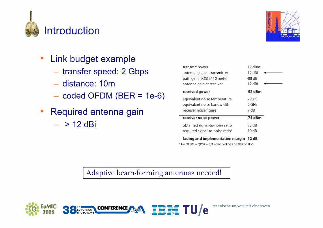
• Link budget example– transfer speed: 2 Gbps– distance: 10m– coded OFDM (BER = 1e-6)
• Required antenna gain– > 12 dBi
Adaptive beam-forming antennas needed!

Introduction
• Integrate into one package– transceiver chip-set– antenna– other passive components

Introduction
• Why is this difficult?– wavelength is small
• high-precision technology is needed– vias do not work well
• relatively large– mismatch– loss
– feed-line loss• large wire inductance (~ ωL)
– dielectric loss (~ ω)• high-quality materials needed
How to do low-cost packaging at mm-wave frequencies?

Antenna considerations
• Antenna requirements– broadband operation
• minimum 5 GHz bandwidth– high radiation efficiency
• low dielectric constant– hemispherical radiation pattern antenna element
• large scan range antenna array– low interconnect loss with Tx/Rx chip
• coplanar feed– easy integration into package
• planar technology
Antenna considerations
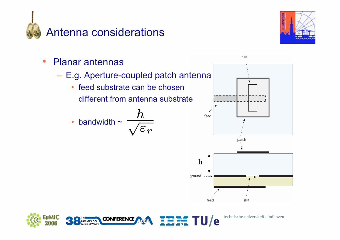
• Planar antennas– E.g. Aperture-coupled patch antenna
• feed substrate can be chosen different from antenna substrate
• bandwidth ~h√εr
h
Antenna considerations
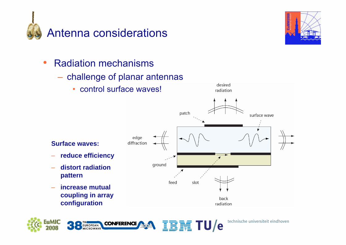
• Radiation mechanisms– challenge of planar antennas
• control surface waves!
Surface waves:
– reduce efficiency
– distort radiation pattern
– increase mutual coupling in array configuration
Antenna considerations
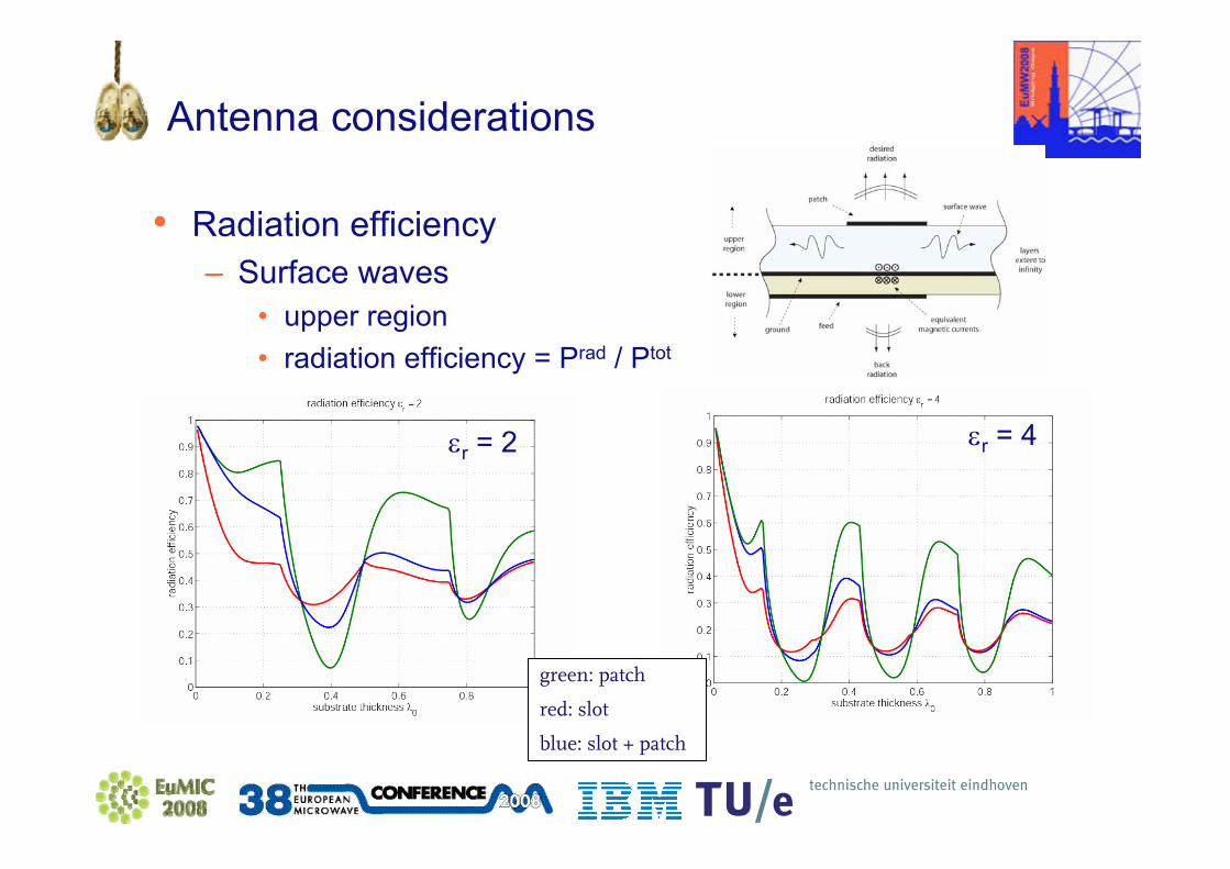
• Radiation efficiency– Surface waves
• upper region• radiation efficiency = Prad / Ptot
green: patch
red: slot
blue: slot + patch
εr = 2 εr = 4

Antenna considerations
• Antenna on chip?
– bandwidth ~
green: patch
red: slot
blue: slot + patch
h√εr
εr = 12

Package considerations
• Package requirements– standard planar manufacturing technology
• low-cost– small feature size
• low tolerances– accurate alignment– candidates
• advanced PCB– thin-film
• LTCC• Silicon-based
14
Package considerations
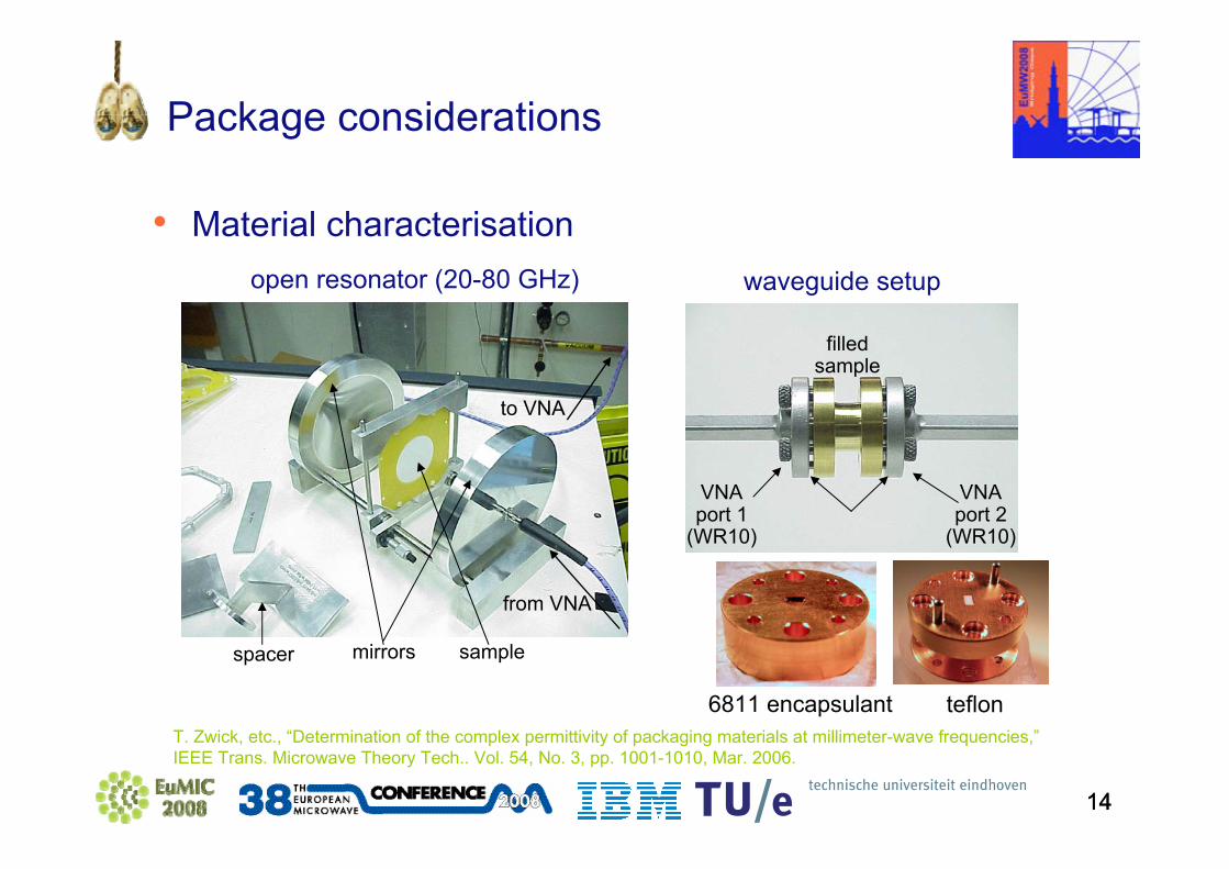
• Material characterisation
14
T. Zwick, etc., “Determination of the complex permittivity of packaging materials at millimeter-wave frequencies,”IEEE Trans. Microwave Theory Tech.. Vol. 54, No. 3, pp. 1001-1010, Mar. 2006.
samplemirrorsspacer
from VNA
to VNA
filledsample
VNAport 1
(WR10)
VNAport 2
(WR10)
6811 encapsulant teflon
open resonator (20-80 GHz) waveguide setup
15
Example: Cavity-backed superstrate antenna
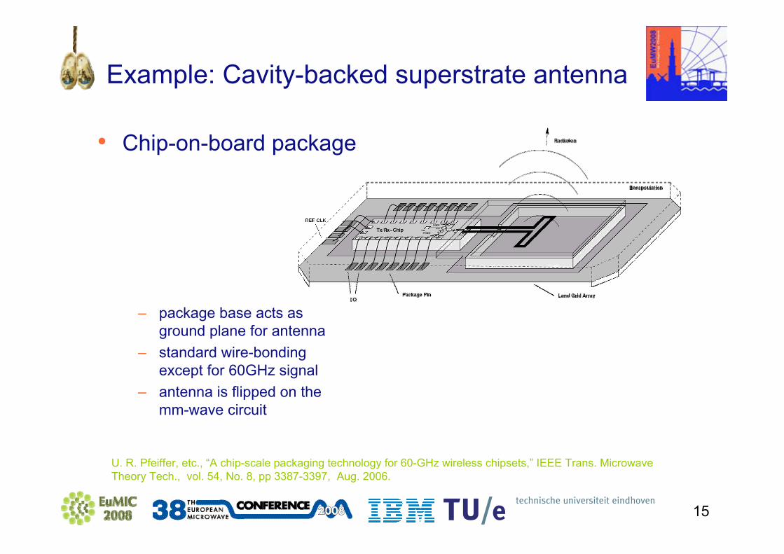
• Chip-on-board package
– package base acts as ground plane for antenna
– standard wire-bonding except for 60GHz signal
– antenna is flipped on the mm-wave circuit
U. R. Pfeiffer, etc., “A chip-scale packaging technology for 60-GHz wireless chipsets,” IEEE Trans. Microwave Theory Tech., vol. 54, No. 8, pp 3387-3397, Aug. 2006.
16
Example: Cavity-backed superstrate antenna
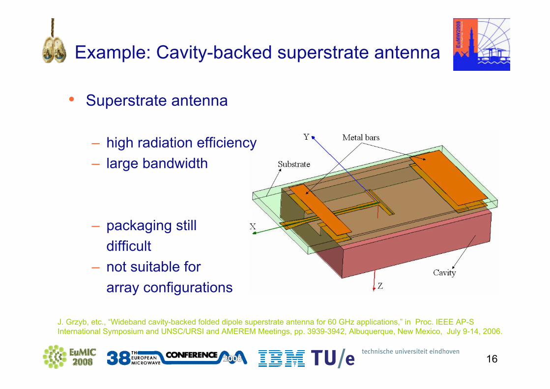
• Superstrate antenna
– high radiation efficiency– large bandwidth
– packaging still difficult
– not suitable forarray configurations
J. Grzyb, etc., “Wideband cavity-backed folded dipole superstrate antenna for 60 GHz applications,” in Proc. IEEE AP-S International Symposium and UNSC/URSI and AMEREM Meetings, pp. 3939-3942, Albuquerque, New Mexico, July 9-14, 2006.
17
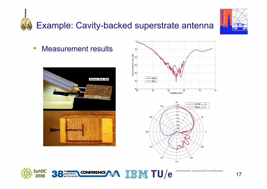
Example: Cavity-backed superstrate antenna
• Measurement results

18
Example: Cavity-backed superstrate antenna
• Chip is molded with standard glob-top material
• Optional antenna window.
19
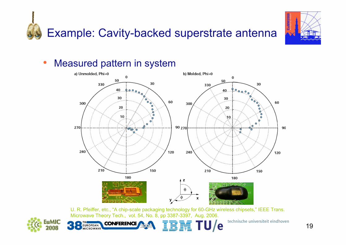
Example: Cavity-backed superstrate antenna
• Measured pattern in system
U. R. Pfeiffer, etc., “A chip-scale packaging technology for 60-GHz wireless chipsets,” IEEE Trans. Microwave Theory Tech., vol. 54, No. 8, pp 3387-3397, Aug. 2006.

20
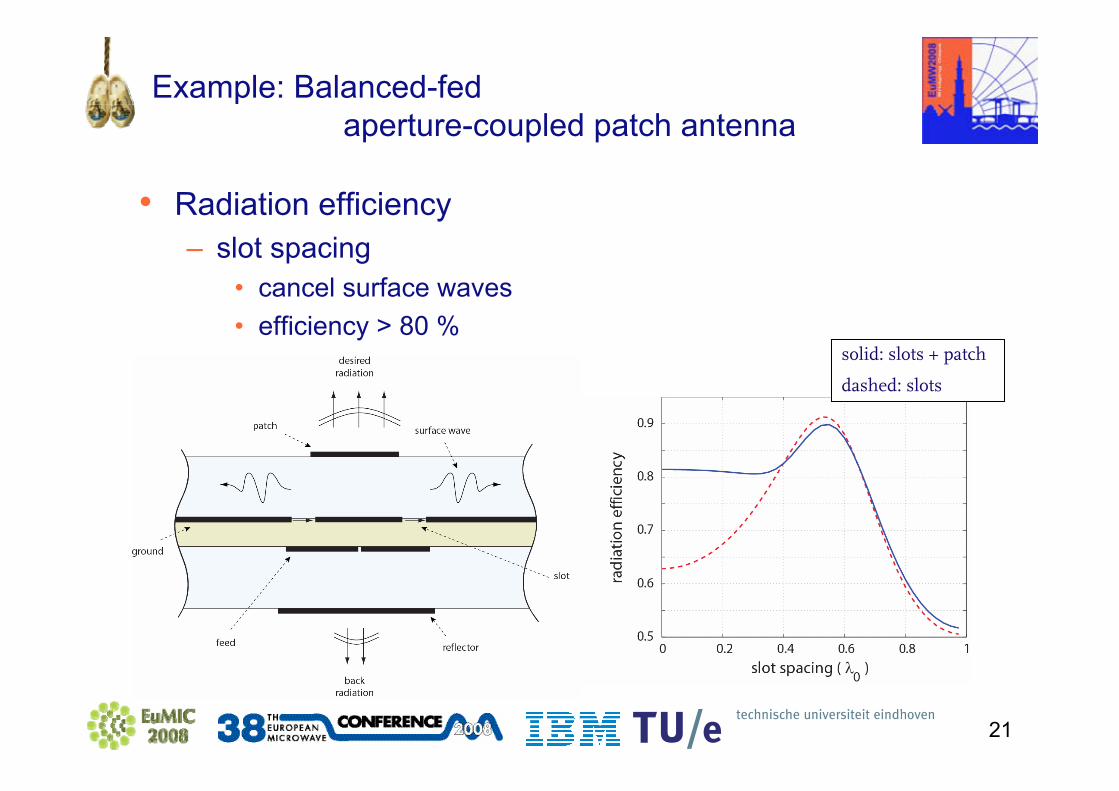
Example: Balanced-fed aperture-coupled patch antenna
– PCB technology– no vias– high radiation efficiency
• >80%– bandwidth
• 10-15 %
J.A.G. Akkermans, etc., “Design of a millimeter-wave balanced-fed aperture-coupled patch antenna” in proc. EuCAP, ESA SP626, (Nice, France), November 2006.
21
Example: Balanced-fed aperture-coupled patch antenna
• Radiation efficiency– slot spacing
• cancel surface waves• efficiency > 80 %
solid: slots + patch
dashed: slots

22
Example: Balanced-fed aperture-coupled patch antenna
• Measurement setup– RF probe– transition
• CPW - MS– balun
– problem:flow of adhesiveinto open cavity

23
Example: Balanced-fed aperture-coupled patch antenna
• Radiation pattern measurement

24
Example: Balanced-fed aperture-coupled patch antenna
• Measurement results
- simulation (red)
- measurement (black)
- time-gated measurement (blue)
- simulation (dashed)
- measurement (solid)

25
Example: LTCC package effort
• LTCC antenna-in-package– slot dipole (differential)– yagi (single-ended)
• chip interconnect with bondwires
Y. P. Zhang, etc., ``Antenna-in-package in LTCC for 60 GHz radio," in Proc. IEEE International Workshop on Antenna Technology, Cambridge, UK, March 21-23, 2007.
26
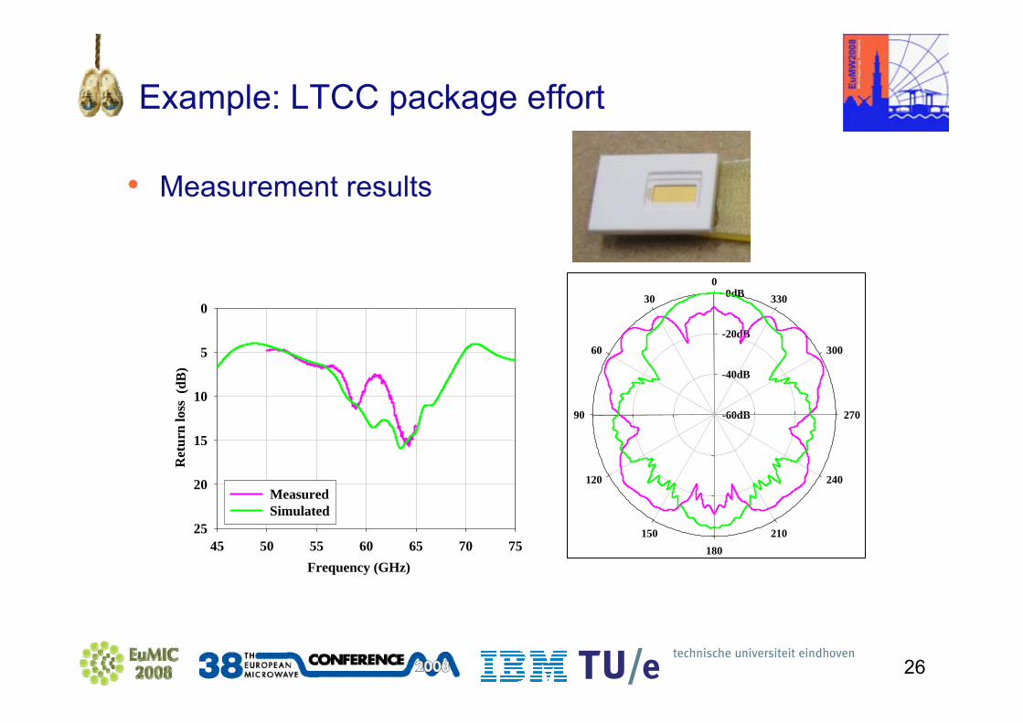
Example: LTCC package effort
• Measurement results
Frequency (GHz)45 50 55 60 65 70 75
Ret
urn
loss
(dB
)
0
5
10
15
20
25
MeasuredSimulated
-60dB
-40dB
-20dB
0dB0
30
60
90
120
150180
210
240
270
300
330

27
Example: LTCC package effort
• 2nd generation– holes to reduce effective
dielectric constant– under evaluation
10 mm

28
Example: Si-based packaging
antenna cavity
radiationantenna structure
probe pad
antenna feed line
150um
600umantenna cavity
radiationantenna structure
probe pad
antenna feed line
150um
600um
Buried SiGe chip
Antenna cavity
Hermetically sealed MEMS
switch
Antenna
Through-wafer vias
Radiation
Bonding
SiGe RF IC
~10 mm
• package concept– cavity-backed
antenna– high-resolution
process
• antenna test
structure
N. Hoivik, etc., “High-efficiency 60 GHZ antenna fabricated using low-cost silicon micromaching techniques,” in Proc. IEEE AP-S International Symposium, pp. 5043-5046, Honolulu, Hawaii, June 10-15, 2007.

29
Example: Si-based packaging
• The antenna is fabricated using 1.2 μm thick Cu
• Si wafers were thinned after processing from 725 μm to 150 μm using a back-side grinding process
2.2 mm
0.7 mm0.7 mm
Top view of antenna – High resistivity Si
Antenna cavity – doped Si
Antenna cavity
5 um Cu

30
Example: Si-based packaging
• Measurement results– S11 in good agreement with
simulations– high efficiency– gain 6-8 dBi

31
Example: Beam-forming antenna array
• Beam-forming antenna array– 6-element circular array– feed network designed for
scan to θ = 0, 30, 60 degrees– problem:
large feed-line losses(1.3 dB/cm)
J.A.G. Akkermans, etc., “Planar beam-forming array for broadband communication in the 60 GHz band”, EuCAP 2007, Edinburgh, UK, November 2007
32
Example: Beam-forming antenna array
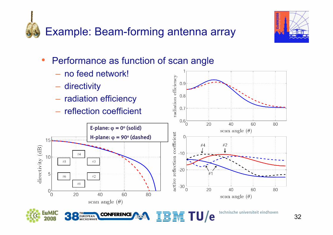
• Performance as function of scan angle– no feed network!– directivity– radiation efficiency– reflection coefficient
E-plane: ϕ = 0o (solid)
H-plane: ϕ = 90o (dashed)

33
Example: Beam-forming antenna array
• Measurement results– beam-forming to 0, 30, 45 degrees
- simulation (dashed)
- measurement (solid)

34
Conclusions
• A lot of work is going on in millimeter-wave packaging
• Challenges– low-cost solution
• planar technology– efficient
• control surface waves• coplanar feed
– flexible• support antenna arrays
• The all-in-one solution is not presented yet!