ap2112 voutin 600ma cmos ldo regulator … · high voltage enable logic high, regulator on 1.5 —...
TRANSCRIPT

AP2112 Document number: DS39724 Rev. 2 - 2
1 of 18 www.diodes.com
June 2017 © Diodes Incorporated
AP2112
600mA CMOS LDO REGULATOR WITH ENABLE
Description
The AP2112 is CMOS process low dropout linear regulator with
enable function, the regulator delivers a guaranteed 600mA (min.)
continuous load current.
The AP2112 is available with a fixed output voltage of 1.2V, 1.8V,
2.5V, 2.6V, or 3.3V. The LDO has an output accuracy of ±1.5% and a
very fast loop response providing excellent performance for dealing
with line and load transients. The AP2112 includes an auto discharge
function which connects the output to ground via 60 of resistance
when the device is disabled.
The regulator features low power consumption, and provides SOT25,
SOT89-5, and SO-8 packages. Previously SOT-23-5, SOT-89-5 and
SOIC-8 packages were respectively identified as SOT23-5, SOT89-5
and SO-8 but have been renamed to match the latest Diodes
Incorporated‘s nomenclature.
Features
Output Voltage Accuracy: ±1.5%
Output Current: 600mA (Min.)
Foldback Short Current Protection: 50mA
Enable Function to Turn ON/OFF VOUT
Low Dropout Voltage (3.3V): 250mV (Typ.) @IOUT = 600mA
Excellent Load Regulation: 0.2%/A (Typ.)
Excellent Line Regulation: 0.02%/V (Typ.)
Low Quiescent Current: 55µA (Typ.)
Low Standby Current: 0.01µA (Typ.)
Low Output Noise: 50µVRMS
PSRR: 100Hz -65dB, 1kHz -65dB
OTSD Protection
Stable with 1.0µF Flexible Cap: Ceramic, Tantalum and
Aluminum Electrolytic
Operation Temperature Range: -40°C to +85°C
ESD: MM 400V, HBM 4000V
Totally Lead-Free & Fully RoHS Compliant (Notes 1 & 2)
Halogen and Antimony Free. “Green” Device (Note 3)
Applications
Laptop Computer
LCD Monitor
Portable DVD
Pin Assignments
(Top View) (Top View)
1
2
3 4
5 VOUT
NCEN
GND
VIN 1
2
3
4
8
7
6
5
VOUT
NC
VIN
GND
GND
EN
NC
NC
SOT25 SO-8
(Top View) (Top View)
1 2 3
45
VOUT VIN
NC GND EN
1 2 3
45
VOUT VIN
NCGNDEN (R5 Package) (R5A Package)
SOT89-5 (Option 1)
(Top View) (Top View)
1 2 3
45
VOUT VIN
NC GND EN
1 2 3
45
VOUT VIN
EN GND NC (R5 Package) (R5A Package)
SOT89-5 (Option 2)
Notes: 1. No purposely added lead. Fully EU Directive 2002/95/EC (RoHS) & 2011/65/EU (RoHS 2) compliant.
2. See http://www.diodes.com/quality/lead_free.html for more information about Diodes Incorporated‘s definitions of Halogen- and Antimony-free, "Green"
and Lead-free.
3. Halogen- and Antimony-free "Green‖ products are defined as those which contain <900ppm bromine, <900ppm chlorine (<1500ppm total Br + Cl) and
<1000ppm antimony compounds.

AP2112 Document number: DS39724 Rev. 2 - 2
2 of 18 www.diodes.com
June 2017 © Diodes Incorporated
AP2112
Typical Applications Circuit (Note 4)
AP2112
GND
VIN
CIN
VOUT
COUT
OFF
VEN
VIN VOUT
1mF
1.2V/1.8V/
2.5V/2.6V/
3.3V
1mF
ON
Note 4: It is recommended to use X7R or X5R dielectric capacitor if 1.0µF ceramic capacitor is selected as input/output capacitors.
Pin Descriptions
Pin Number Pin Name Function
SOT25 SOT89-5 SO-8
1 4 8 VIN Input Voltage
2 2 6, 7 GND GND
3 3 (R5)
5 EN Chip Enable, H – normal work, L – shutdown output 1 (R5A)
— 1 (R5)
2, 3, 4 NC No Connection 3 (R5A)
5 5 1 VOUT Output Voltage
Functional Block Diagram
Shutdown Logic
Thermal
Shutdown
Foldback
Current Limit
VREF
GND
EN
VOUT
VIN
3M
4(4)8[1]
2(2)6,7[2]
3(1)5[3]
5(5)1[5]
A (B)C[D] A: SOT89-5 (R5) B: SOT89-5 (R5A) C: SO-8 D: SOT25

AP2112 Document number: DS39724 Rev. 2 - 2
3 of 18 www.diodes.com
June 2017 © Diodes Incorporated
AP2112
Absolute Maximum Ratings (Note 5)
Symbol Parameter Rating Unit
VCC Power Supply Voltage 6.5 V
TJ Operating Junction Temperature Range +150 °C
TSTG Storage Temperature Range -65 to +150 °C
TLEAD Lead Temperature (Soldering, 10 Seconds) +260 °C
θJA Thermal Resistance (Junction to Ambient)(No Heatsink)
SOT25 184
°C/W SO-8 114
SOT89-5 120
— ESD (Machine Model) 400 V
— ESD (Human Body Model) 4000 V
Note 5: Stresses greater than those listed under ―Absolute Maximum Ratings‖ may cause permanent damage to the device. These are stress ratings only, and
functional operation of the device at these or any other conditions beyond those indicated under ―Recommended Operating Conditions‖ is not implied.
Exposure to ―Absolute Maximum Ratings‖ for extended periods may affect device reliability.
Recommended Operating Conditions
Symbol Parameter Min Max Unit
VIN Supply Voltage 2.5 6.0 V
TA Ambient Operation Temperature Range -40 +85 °C

AP2112 Document number: DS39724 Rev. 2 - 2
4 of 18 www.diodes.com
June 2017 © Diodes Incorporated
AP2112
Electrical Characteristics
AP2112-1.2 Electrical Characteristics (@VIN = 2.5V, CIN = 1.0µF (Ceramic), COUT = 1.0µF (Ceramic), Typical TA = +25°C,
unless otherwise specified (Note 6))
Symbol Parameter Conditions Min Typ Max Unit
VOUT Output Voltage VIN = 2.5V, 1mA ≤ IOUT ≤ 30mA VOUT
*98.5% 1.2
VOUT
*101.5% V
IOUT(MAX) Maximum Output Current VIN = 2.5V, VOUT = 1.182V to 1.218V 600 — — mA
(∆VOUT/VOUT)/∆IOUT Load Regulation VIN = 2.5V, 1mA ≤ IOUT ≤ 600mA -1 0.2 1 %/A
(∆VOUT/VOUT)/∆VIN Line Regulation 2.5V ≤ VIN ≤ 6V, IOUT = 30mA -0.1 0.02 0.1 %/V
VDROP Dropout Voltage
IOUT = 10mA — 1000 1300
mV IOUT = 300mA — 1000 1300
IOUT = 600mA — 1000 1300
IQ Quiescent Current VIN = 2.5V, IOUT = 0mA — 55 80 µA
ISTD Standby Current VIN = 2.5V, VEN in OFF mode — 0.01 1.0 µA
PSRR Power Supply Rejection Ratio
Ripple 0.5Vp-p
VIN = 2.5V,
IOUT = 100mA
f = 100Hz — 65 —
dB
f = 1kHz — 65 —
(∆VOUT/VOUT)/∆T Output Voltage Temperature
Coefficient
IOUT = 30mA
TA = -40°C to +85°C — ±100 — ppm/°C
ISHORT Short Current Limit VOUT = 0V — 50 — mA
VNOISE RMS Output Noise No Load, 10Hz ≤ f ≤ 100kHz — 50 — µVRMS
VIH VEN High Voltage Enable logic high, regulator on 1.5 — 6.0
V
VIL VEN Low Voltage Enable logic low, regulator off 0 — 0.4
tS Start-up Time No Load — 20 — µs
RPD EN Pull Down Resistor — — 3.0 — MΩ
RDCHG VOUT Discharge Resistor Set EN pin at Low — 60 — Ω
TOTSD Thermal Shutdown Temperature — — +160 —
°C
THYOTSD Thermal Shutdown Hysteresis — — +25 —
θJC Thermal Resistance
(Junction to Case)
SOT25 — 96 —
°C/W SO-8 — 75 —
SOT89-5 — 47 —
Note 6: Production testing at TA = +25°C. Over temperature specifications guaranteed by design only.

AP2112 Document number: DS39724 Rev. 2 - 2
5 of 18 www.diodes.com
June 2017 © Diodes Incorporated
AP2112
Electrical Characteristics (Cont.)
AP2112-1.8 Electrical Characteristics (@VIN = 2.8V, CIN = 1.0µF (Ceramic), COUT = 1.0µF (Ceramic), Typical TA = +25°C,
unless otherwise specified (Note 6))
Symbol Parameter Conditions Min Typ Max Unit
VOUT Output Voltage VIN = 2.8V, 1mA ≤ IOUT ≤ 30mA VOUT
*98.5% 1.8
VOUT
*101.5% V
IOUT(MAX) Maximum Output Current VIN = 2.8V, VOUT = 1.773V to 1.827V 600 — — mA
(∆VOUT/VOUT)/∆IOUT Load Regulation VOUT = 1.8V, VIN = VOUT+1V,
1mA ≤ IOUT ≤ 600mA -1 0.2 1 %/A
(∆VOUT/VOUT)/∆VIN Line Regulation 2.8V ≤ VIN ≤ 6V, IOUT = 30mA -0.1 0.02 0.1 %/V
VDROP Dropout Voltage
IOUT = 10mA — 500 700
mV IOUT = 300mA — 500 700
IOUT = 600mA — 500 700
IQ Quiescent Current VIN = 2.8V, IOUT = 0mA — 55 80 µA
ISTD Standby Current VIN = 2.8V, VEN in OFF mode — 0.01 1.0 µA
PSRR Power Supply Rejection Ratio
Ripple 0.5Vp-p
VIN = 2.8V,
IOUT = 100mA
f = 100Hz — 65 —
dB
f = 1kHz — 65 —
(∆VOUT/VOUT)/∆T Output Voltage Temperature
Coefficient
IOUT = 30mA
TA = -40°C to +85°C — ±100 — ppm/°C
ISHORT Short Current Limit VOUT = 0V — 50 — mA
VNOISE RMS Output Noise No Load, 10Hz ≤ f ≤ 100kHz — 50 — µVRMS
VIH VEN High Voltage Enable logic high, regulator on 1.5 — 6.0
V
VIL VEN Low Voltage Enable logic low, regulator off 0 — 0.4
tS Start-up Time No Load — 20 — µs
RPD EN Pull Down Resistor — — 3.0 — MΩ
RDCHG VOUT Discharge Resistor Set EN pin at Low — 60 — Ω
TOTSD Thermal Shutdown Temperature — — +160 —
°C
THYOTSD Thermal Shutdown Hysteresis — — +25 —
θJC Thermal Resistance
(Junction to Case)
SOT25 — 96 —
°C/W SO-8 — 75 —
SOT89-5 — 47 —
Note 6: Production testing at TA = +25°C. Over temperature specifications guaranteed by design only.

AP2112 Document number: DS39724 Rev. 2 - 2
6 of 18 www.diodes.com
June 2017 © Diodes Incorporated
AP2112
Electrical Characteristics (Cont.)
AP2112-2.5 Electrical Characteristics (@VIN = 3.5V, CIN = 1.0µF (Ceramic), COUT = 1.0µF (Ceramic), Typical TA = +25°C,
unless otherwise specified (Note 6))
Symbol Parameter Conditions Min Typ Max Unit
VOUT Output Voltage VIN = 3.5V, 1mA ≤ IOUT ≤ 30mA VOUT
*98.5% 2.5
VOUT
*101.5% V
IOUT(MAX) Maximum Output Current VIN = 3.5V,
VOUT = 2.463V to 2.537V 600 — — mA
(∆VOUT/VOUT)/∆IOUT Load Regulation VOUT = 2.5V, VIN = VOUT+1V,
1mA ≤ IOUT ≤ 600mA -1 0.2 1 %/A
(∆VOUT/VOUT)/∆VIN Line Regulation 3.5V ≤ VIN ≤ 6V, IOUT = 30mA -0.1 0.02 0.1 %/V
VDROP Dropout Voltage
IOUT = 10mA — 5 8
mV IOUT = 300mA — 125 200
IOUT = 600mA — 250 400
IQ Quiescent Current VIN = 3.5V, IOUT = 0mA — 55 80 µA
ISTD Standby Current VIN = 3.5V, VEN in OFF mode — 0.01 1.0 µA
PSRR Power Supply Rejection Ratio
Ripple 0.5Vp-p
VIN = 3.5V,
IOUT = 100mA
f = 100Hz — 65 —
dB
f = 1KHz — 65 —
(∆VOUT/VOUT)/∆T Output Voltage Temperature
Coefficient
IOUT = 30mA
TA = -40°C to +85°C — ±100 — ppm/°C
ISHORT Short Current Limit VOUT = 0V — 50 — mA
VNOISE RMS Output Noise No Load, 10Hz ≤ f ≤ 100kHz — 50 — µVRMS
VIH VEN High Voltage Enable logic high, regulator on 1.5 — 6.0
V
VIL VEN Low Voltage Enable logic low, regulator off 0 — 0.4
tS Start-up Time No Load — 20 — µs
RPD EN Pull Down Resistor — — 3.0 — MΩ
RDCHG VOUT Discharge Resistor Set EN pin at Low — 60 — Ω
TOTSD Thermal Shutdown Temperature — — +160 —
°C
THYOTSD Thermal Shutdown Hysteresis — — +25 —
θJC Thermal Resistance
(Junction to Case)
SOT25 — 96 —
°C/W SO-8 — 75 —
SOT89-5 — 47 —
Note 6: Production testing at TA = +25°C. Over temperature specifications guaranteed by design only.

AP2112 Document number: DS39724 Rev. 2 - 2
7 of 18 www.diodes.com
June 2017 © Diodes Incorporated
AP2112
Electrical Characteristics (Cont.)
AP2112-2.6 Electrical Characteristics (@VIN = 3.6V, CIN = 1.0µF (Ceramic), COUT = 1.0µF (Ceramic), Typical TA = +25°C,
unless otherwise specified (Note 6))
Symbol Parameter Conditions Min Typ Max Unit
VOUT Output Voltage VIN = 3.6V, 1mA ≤ IOUT ≤ 30mA VOUT
*98.5% 2.6
VOUT
*101.5% V
IOUT(MAX) Maximum Output Current VIN = 3.6V,
VOUT = 2.561V to 2.639V 600 — — mA
(∆VOUT/VOUT)/∆IOUT Load Regulation VOUT = 2.6V, VIN = VOUT+1V,
1mA ≤ IOUT ≤ 600mA -1 0.2 1 %/A
(∆VOUT/VOUT)/∆VIN Line Regulation 3.6V ≤ VIN ≤ 6V, IOUT = 30mA -0.1 0.02 0.1 %/V
VDROP Dropout Voltage
IOUT = 10mA — 5 8
mV IOUT = 300mA — 125 200
IOUT = 600mA — 250 400
IQ Quiescent Current VIN = 3.6V, IOUT = 0mA — 55 80 µA
ISTD Standby Current VIN = 3.6V, VEN in OFF mode — 0.01 1.0 µA
PSRR Power Supply Rejection Ratio
Ripple 0.5Vp-p
VIN = 3.6V,
IOUT = 100mA
f = 100Hz — 65 —
dB
f = 1kHz — 65 —
(∆VOUT/VOUT)/∆T Output Voltage
Temperature Coefficient
IOUT = 30mA
TA = -40°C to +85°C — ±100 — ppm/°C
ISHORT Short Current Limit VOUT = 0V — 50 — mA
VNOISE RMS Output Noise No Load, 10Hz ≤ f ≤ 100kHz — 50 — µVRMS
VIH VEN High Voltage Enable logic high, regulator on 1.5 — 6.0
V
VIL VEN Low Voltage Enable logic low, regulator off 0 — 0.4
tS Start-up Time No Load — 20 — µs
RPD EN Pull Down Resistor — — 3.0 — MΩ
RDCHG VOUT Discharge Resistor Set EN pin at Low — 60 — Ω
TOTSD Thermal Shutdown Temperature — — +160 —
°C
THYOTSD Thermal Shutdown Hysteresis — — +25 —
θJC Thermal Resistance
(Junction to Case)
SOT25 — 96 —
°C/W SO-8 — 75 —
SOT89-5 — 47 —
Note 6: Production testing at TA = +25°C. Over temperature specifications guaranteed by design only.
AP2112 Document number: DS39724 Rev. 2 - 2
8 of 18 www.diodes.com
June 2017 © Diodes Incorporated
AP2112
Electrical Characteristics (Cont.)
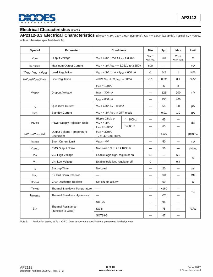
AP2112-3.3 Electrical Characteristics (@VIN = 4.3V, CIN = 1.0µF (Ceramic), COUT = 1.0µF (Ceramic), Typical TA = +25°C,
unless otherwise specified (Note 6))
Symbol Parameter Conditions Min Typ Max Unit
VOUT Output Voltage VIN = 4.3V, 1mA ≤ IOUT ≤ 30mA VOUT
*98.5% 3.3
VOUT
*101.5% V
IOUT(MAX) Maximum Output Current VIN = 4.3V, VOUT = 3.251V to 3.350V 600 — — mA
(∆VOUT/VOUT)/∆IOUT Load Regulation VIN = 4.3V, 1mA ≤ IOUT ≤ 600mA -1 0.2 1 %/A
(∆VOUT/VOUT)/∆VIN Line Regulation 4.3V≤ VIN ≤ 6V, IOUT = 30mA -0.1 0.02 0.1 %/V
VDROP Dropout Voltage
IOUT = 10mA — 5 8
mV IOUT = 300mA — 125 200
IOUT = 600mA — 250 400
IQ Quiescent Current VIN = 4.3V, IOUT = 0mA — 55 80 µA
ISTD Standby Current VIN = 4.3V, VEN in OFF mode — 0.01 1.0 µA
PSRR Power Supply Rejection Ratio
Ripple 0.5Vp-p
VIN = 4.3V,
IOUT = 100mA
f = 100Hz — 65 —
dB
f = 1kHz — 65 —
(∆VOUT/VOUT)/∆T Output Voltage Temperature
Coefficient
IOUT = 30mA
TA = -40°C to +85°C — ±100 — ppm/°C
ISHORT Short Current Limit VOUT = 0V — 50 — mA
VNOISE RMS Output Noise No Load, 10Hz ≤ f ≤ 100kHz — 50 — µVRMS
VIH VEN High Voltage Enable logic high, regulator on 1.5 — 6.0
V
VIL VEN Low Voltage Enable logic low, regulator off 0 — 0.4
tS Start-up Time No Load — 20 — µs
RPD EN Pull Down Resistor — — 3.0 — MΩ
RDCHG VOUT Discharge Resistor Set EN pin at Low — 60 — Ω
TOTSD Thermal Shutdown Temperature — — +160 —
°C
THYOTSD Thermal Shutdown Hysteresis — — +25 —
θJC Thermal Resistance
(Junction to Case)
SOT25 — 96 —
°C/W SO-8 — 75 —
SOT89-5 — 47 —
Note 6: Production testing at TA = +25°C. Over temperature specifications guaranteed by design only.

AP2112 Document number: DS39724 Rev. 2 - 2
9 of 18 www.diodes.com
June 2017 © Diodes Incorporated
AP2112
Performance Characteristics
Output Voltage vs. Input Voltage Output Voltage vs. Input Voltage
Quiescent Current vs. Temperature Quiescent Current vs. Input Voltage
Output Voltage vs. Temperature Output Voltage vs. Temperature
0.0 0.5 1.0 1.5 2.0 2.5 3.0 3.5 4.0 4.5 5.0 5.5 6.0
0.0
0.2
0.4
0.6
0.8
1.0
1.2
1.4
1.6
NO Load
TA=-40
oC
TA=25
oC
TA=85
oC
VOUT
=1.2V
Ou
tpu
t V
olta
ge
(V
)
Input Voltage (V)
0.0 0.5 1.0 1.5 2.0 2.5 3.0 3.5 4.0 4.5 5.0 5.5 6.00.0
0.5
1.0
1.5
2.0
2.5
3.0
3.5
4.0
Ou
tpu
t V
olta
ge
(V
)
Input Voltage (V)
TA=-40
oC
TA=25
oC
TA=85
oC
VOUT
=3.3V
No Load
-40.0 -20.0 0.0 20.0 40.0 60.0 80.046
48
50
52
54
56
58
60
62
64
66
68
70
VIN
=2.5V
No Load
Qu
iesce
nt C
urr
en
t (m
A)
Temperature (oC)
1.0 1.5 2.0 2.5 3.0 3.5 4.0 4.5 5.0 5.5 6.0
0
10
20
30
40
50
60
70
Qu
iesce
nt C
urr
en
t (m
A)
TA=-40
OC
TA=25
OC
TA=85
OC
No Load
Input Voltage (V)
-40 -20 0 20 40 60 803.25
3.26
3.27
3.28
3.29
3.30
3.31
3.32
3.33
3.34
3.35
Ou
tpu
t V
olta
ge
(V
)
Temperature(oC)
IOUT
=10mA
IOUT
=100mA
IOUT
=300mA
IOUT
=600mA
VIN
=4.3V
CIN
=1mF
COUT
=1mF
-40.0 -20.0 0.0 20.0 40.0 60.0 80.01.200
1.202
1.204
1.206
1.208
1.210
IOUT
=300mA
IOUT
=600mA
IOUT
=10mA
IOUT
=100mA
VIN
=2.5V
CIN
=1mF
COUT
=1mF
Ou
tpu
t V
olta
ge
(V
)
Temperature (oC)

AP2112 Document number: DS39724 Rev. 2 - 2
10 of 18 www.diodes.com
June 2017 © Diodes Incorporated
AP2112
Performance Characteristics (Cont.)
Output Voltage vs. Output Current Output Voltage vs. Output Current
Output Voltage vs. Output Current Output Voltage vs. Output Current
Dropout Voltage vs. Output Current Ground Current vs. Output Current
0.0 0.1 0.2 0.3 0.4 0.5 0.6 0.7 0.8 0.9 1.0
-0.1
0.0
0.1
0.2
0.3
0.4
0.5
0.6
0.7
0.8
0.9
1.0
1.1
1.2
1.3
VIN
=2.5V
Ou
tpu
t V
olta
ge
(V
)
Output Current (A)
TA= -40
oC
TA=25
oC
TA=85
oC
0.0 0.1 0.2 0.3 0.4 0.5 0.6 0.7 0.8 0.9 1.0-0.5
0.0
0.5
1.0
1.5
2.0
2.5
3.0
3.5
4.0
Ou
tpu
t V
olta
ge
(V
)
Output Current (A)
TA=-40
oC
TA= 25
oC
TA= 85
oC
VIN
=4.3V
0.0 0.1 0.2 0.3 0.4 0.5 0.6 0.7 0.8 0.9 1.0
0.0
0.2
0.4
0.6
0.8
1.0
1.2
TA=25
oC
CIN
=1mF
COUT
=1mF
VIN
=5V
VIN
=2V
VIN
=5.5V
VIN
=6V
VIN
=2.5V
Ou
tpu
t V
olta
ge
(V
)
Output Current (A)
0.0 0.1 0.2 0.3 0.4 0.5 0.6 0.7 0.8 0.9 1.0
0.0
0.5
1.0
1.5
2.0
2.5
3.0
3.5
4.0
Ou
tpu
t V
olta
ge
(V
)
Output Current (A)
VIN
=4.0V
VIN
=4.3V
VIN
=5.0V
VIN
=5.5V
VIN
=6.0V
TA=25
oC
CIN
=1mF
COUT
=1mF
0.0 0.1 0.2 0.3 0.4 0.5 0.640
60
80
100
120
140
160
180
200
220
240
260
Gro
un
d C
urr
en
t (m
A)
Output Current (A)
TA=-40
oC
TA= 25
oC
TA= 85
oC
VIN
=4.3V
0.0 0.1 0.2 0.3 0.4 0.5 0.60
50
100
150
200
250
300
350
Dro
po
ut V
olta
ge
(m
V)
Output Current (A)
TA=-40
oC
TA= 25
oC
TA= 85
oC
VOUT
=3.3V

AP2112 Document number: DS39724 Rev. 2 - 2
11 of 18 www.diodes.com
June 2017 © Diodes Incorporated
AP2112
Performance Characteristics (Cont.)
PSRR vs. Frequency Load Transient
Enable On Enable Off
Application Note
In some unusual applications where a current load could be present at the output before the part is enabled the fold back current limiting may
prevent the part from starting. Applications with multiple supplies or negative supplies need to be evaluated for this possibility. Product testing
where a current source is applied before the part is enabled could be another area of concern. With a normal load as shown below there is no
interference of the fold back current limiting circuit.
20ms/div
100 1k 10k 100k
30
35
40
45
50
55
60
65
70
IOUT
=10mA
IOUT
=100mA
IOUT
=300mA
VOUT
=1.2V
PS
RR
(d
B)
Frequency (Hz)
20
VIN
=2.5V
Ripple=0.5V
0mA
VIN=2.5V, CIN=1mF, COUT=1mF
CH1: VOUT
10mV/div
CH2: IOUT
200mA/div
600mA
VIN (2V/div)
VIN
(2V/div)
VIN
(2V/div)
VEN
(2V/div)
VEN
(2V/div)
VOUT
(2V/div)
VOUT
(2V/div)
20ms/div
VIN
(2V/div)
VIN
(2V/div)
VEN
(2V/div)
VEN
(2V/div)
VOUT
(2V/div)
VOUT
(2V/div)
200ms/div
0.0 0.1 0.2 0.3 0.4 0.5 0.6 0.7 0.8 0.9 1.0
0.0
0.5
1.0
1.5
2.0
2.5
3.0
3.5
4.0
Ou
tpu
t V
olta
ge
(V
)
Output Current (A)
VIN
=4.0V
VIN
=4.3V
VIN
=5.0V
VIN
=5.5V
VIN
=6.0V
TA=25
oC
CIN
=1mF
COUT
=1mFLoad Line

AP2112 Document number: DS39724 Rev. 2 - 2
12 of 18 www.diodes.com
June 2017 © Diodes Incorporated
AP2112
Ordering Information
AP2112 X - X X X
PackingPackage
K : SOT25M : SO-8
Product Name Output Voltage
1.8 : 1.8V2.5 : 2.5V2.6 : 2.6V
1.2 : 1.2V
RoHS/Green
R5/R5A : SOT89-5
TR : Tape & Reel G1 : Green
3.3 : 3.3V
Package Temperature
Range Condition Part Number Marking ID Packing
SOT25 -40 to +85°C
1.2V AP2112K-1.2TRG1 G3L 3000/7‖/Tape & Reel
1.8V AP2112K-1.8TRG1 G3M 3000/7‖/Tape & Reel
2.5V AP2112K-2.5TRG1 G3N 3000/7‖/Tape & Reel
2.6V AP2112K-2.6TRG1 G5N 3000/7‖/Tape & Reel
3.3V AP2112K-3.3TRG1 G3P 3000/7‖/Tape & Reel
SO-8 -40 to +85°C
1.2V AP2112M-1.2TRG1 2112M-1.2G1 4000/13‖/Tape & Reel
1.8V AP2112M-1.8TRG1 2112M-1.8G1 4000/13‖/Tape & Reel
2.5V AP2112M-2.5TRG1 2112M-2.5G1 4000/13‖/Tape & Reel
2.6V AP2112M-2.6TRG1 2112M-2.6G1 4000/13‖/Tape & Reel
3.3V AP2112M-3.3TRG1 2112M-3.3G1 4000/13‖/Tape & Reel
SOT89-5 -40 to +85°C
1.2V(R5) AP2112R5-1.2TRG1 G37D 1000/7‖/Tape & Reel
1.8V(R5) AP2112R5-1.8TRG1 G37E 1000/7‖/Tape & Reel
2.5V(R5) AP2112R5-2.5TRG1 G37F 1000/7‖/Tape & Reel
2.6V(R5) AP2112R5-2.6TRG1 G13F 1000/7‖/Tape & Reel
3.3V(R5) AP2112R5-3.3TRG1 G37G 1000/7‖/Tape & Reel
SOT89-5 -40 to +85°C
1.2V(R5A) AP2112R5A-1.2TRG1 G33C 1000/7‖/Tape & Reel
1.8V(R5A) AP2112R5A-1.8TRG1 G33E 1000/7‖/Tape & Reel
2.5V(R5A) AP2112R5A-2.5TRG1 G28G 1000/7‖/Tape & Reel
2.6V(R5A) AP2112R5A-2.6TRG1 G13E 1000/7‖/Tape & Reel
3.3V(R5A) AP2112R5A-3.3TRG1 G28H 1000/7‖/Tape & Reel

AP2112 Document number: DS39724 Rev. 2 - 2
13 of 18 www.diodes.com
June 2017 © Diodes Incorporated
AP2112
Marking Information
(1) SOT25
XXX
(2) SO-8
(3) SOT89-5
: Logo XXX : Marking ID (See Ordering Information)
XXXX YWWAXX
First Line: Logo and Marking ID Second line: Date Code Y: Year WW: Work Week of Molding A: Assembly House Code XX: 7
th and 8
th Digits of Batch Number
2112M-X.XG1 YWWAXX
First line: Logo and Marking ID Second line: Date Code Y: Year WW: Work Week of Molding A: Assembly House Code XX: 7
th and 8
th Digits of Batch Number

AP2112 Document number: DS39724 Rev. 2 - 2
14 of 18 www.diodes.com
June 2017 © Diodes Incorporated
AP2112
Package Outline Dimensions (Previously identified as SOT-23-5 for this product)
Please see http://www.diodes.com/package-outlines.html for the latest version.
SOT25
Suggested Pad Layout
Please see http://www.diodes.com/package-outlines.html for the latest version.
SOT25
Note: The suggested land pattern dimensions have been provided for reference only, as actual pad layouts may vary depending on application. These
dimensions may be modified based on user equipment capability or fabrication criteria. A more robust pattern may be desired for wave soldering and is calculated by adding 0.2 mm to the ‗Z‘ dimension. For further information, please reference document IPC-7351A, Naming Convention for Standard SMT Land Patterns, and for International grid details, please see document IEC, Publication 97.
Note: For high voltage applications, the appropriate industry sector guidelines should be considered with regards to creepage and clearance distances
between device Terminals and PCB tracking.
SOT25
Dim Min Max Typ
A 0.35 0.50 0.38
B 1.50 1.70 1.60
C 2.70 3.00 2.80
D - - 0.95
H 2.90 3.10 3.00
J 0.013 0.10 0.05
K 1.00 1.30 1.10
L 0.35 0.55 0.40
M 0.10 0.20 0.15
N 0.70 0.80 0.75
0° 8° -
All Dimensions in mm
Dimensions Value
Z 3.20
G 1.60
X 0.55
Y 0.80 C1 2.40
C2 0.95
A
M
JLD
B C
H
KN
X
Z
Y
C1
C2C2
G

AP2112 Document number: DS39724 Rev. 2 - 2
15 of 18 www.diodes.com
June 2017 © Diodes Incorporated
AP2112
Package Outline Dimensions (All dimensions in mm.) (Previously identified as SOT-89-5 for this product)
SOT89-5
45
1.030(0.041)REF1.550(0.061)REF
4.400(0.173)
4.600(0.181)
0.900(0.035)
1.100(0.043)
3.950(0.156)4.250(0.167)
3.000(0.118)
TYP
0.480(0.019)
2.300(0.091)
2.600(0.102)
0.320(0.013)
3 10
2.060(0.081)REF
0.350(0.014)
0.450(0.018)
R0.150(0.006)
3
10
1.500(0.059)
0.320(0.013)REF
1.620(0.064)REF2.210(0.087)REF
0.320(0.013)
1.800(0.071)
Option 1
1.100(0.043)
0.900(0.035)
TYP
0.540(0.021) 0.540(0.021)
Option 2
1.620(0.064)
1.830(0.072)
R 0.200(0.008)
2.630(0.104)
2.930(0.115)
0.950(0.037)
0.650(0.026)
0.650(0.026)
0.950(0.037)
0.500(0.020)
0.620(0.024)
1.400(0.055)1.600(0.063)
Option 1

AP2112 Document number: DS39724 Rev. 2 - 2
16 of 18 www.diodes.com
June 2017 © Diodes Incorporated
AP2112
Suggested Pad Layout (Previously identified as SOT-89-5 for this product)
SOT89-5
X1
X2Y1
E
Z
Y
X
Dimensions Z
(mm)/(inch) X
(mm)/(inch) X1
(mm)/(inch) X2
(mm)/(inch) Y
(mm)/(inch) Y1
(mm)/(inch) E
(mm)/(inch)
Value 4.600/0.181 0.550/0.022 1.850/0.073 0.800/0.031 1.300/0.051 1.475/0.058 1.500/0.059

AP2112 Document number: DS39724 Rev. 2 - 2
17 of 18 www.diodes.com
June 2017 © Diodes Incorporated
AP2112
Package Outline Dimensions (Previously identified as SOIC-8 for this product) Please see http://www.diodes.com/package-outlines.html for the latest version.
SO-8
SO-8
Dim Min Max Typ
A 1.40 1.50 1.45
A1 0.10 0.20 0.15
b 0.30 0.50 0.40
c 0.15 0.25 0.20
D 4.85 4.95 4.90
E 5.90 6.10 6.00
E1 3.80 3.90 3.85
E0 3.85 3.95 3.90
e -- -- 1.27
h - -- 0.35
L 0.62 0.82 0.72
Q 0.60 0.70 0.65
All Dimensions in mm
Suggested Pad Layout Please see http://www.diodes.com/package-outlines.html for the latest version.
SO-8
Note: The suggested land pattern dimensions have been provided for reference only, as actual pad layouts may vary depending on application. These
dimensions may be modified based on user equipment capability or fabrication criteria. A more robust pattern may be desired for wave soldering and is calculated by adding 0.2 mm to the ‗Z‘ dimension. For further information, please reference document IPC-7351A, Naming Convention for Standard SMT Land Patterns, and for International grid details, please see document IEC, Publication 97.
Note: For high voltage applications, the appropriate industry sector guidelines should be considered with regards to creepage and clearance distances
between device Terminals and PCB tracking.
1
b
e
E
A
A1
9° (All sides)
4° ± 3°
c
Qh
45°
R 0.1
7°
D
E0
E1
LSeating Plane
Gauge Plane
Dimensions Value (in mm)
C 1.27
X 0.802
X1 4.612
Y 1.505
Y1 6.50
C X
Y
Y1
X1

AP2112 Document number: DS39724 Rev. 2 - 2
18 of 18 www.diodes.com
June 2017 © Diodes Incorporated
AP2112
IMPORTANT NOTICE DIODES INCORPORATED MAKES NO WARRANTY OF ANY KIND, EXPRESS OR IMPLIED, WITH REGARDS TO THIS DOCUMENT, INCLUDING, BUT NOT LIMITED TO, THE IMPLIED WARRANTIES OF MERCHANTABILITY AND FITNESS FOR A PARTICULAR PURPOSE (AND THEIR EQUIVALENTS UNDER THE LAWS OF ANY JURISDICTION). Diodes Incorporated and its subsidiaries reserve the right to make modifications, enhancements, improvements, corrections or other changes without further notice to this document and any product described herein. Diodes Incorporated does not assume any liability arising out of the application or use of this document or any product described herein; neither does Diodes Incorporated convey any license under its patent or trademark rights, nor the rights of others. Any Customer or user of this document or products described herein in such applications shall assume all risks of such use and will agree to hold Diodes Incorporated and all the companies whose products are represented on Diodes Incorporated website, harmless against all damages. Diodes Incorporated does not warrant or accept any liability whatsoever in respect of any products purchased through unauthorized sales channel. Should Customers purchase or use Diodes Incorporated products for any unintended or unauthorized application, Customers shall indemnify and hold Diodes Incorporated and its representatives harmless against all claims, damages, expenses, and attorney fees arising out of, directly or indirectly, any claim of personal injury or death associated with such unintended or unauthorized application. Products described herein may be covered by one or more United States, international or foreign patents pending. Product names and markings noted herein may also be covered by one or more United States, international or foreign trademarks. This document is written in English but may be translated into multiple languages for reference. Only the English version of this document is the final and determinative format released by Diodes Incorporated.
LIFE SUPPORT Diodes Incorporated products are specifically not authorized for use as critical components in life support devices or systems without the express written approval of the Chief Executive Officer of Diodes Incorporated. As used herein: A. Life support devices or systems are devices or systems which: 1. are intended to implant into the body, or
2. support or sustain life and whose failure to perform when properly used in accordance with instructions for use provided in the labeling can be reasonably expected to result in significant injury to the user.
B. A critical component is any component in a life support device or system whose failure to perform can be reasonably expected to cause the failure of the life support device or to affect its safety or effectiveness. Customers represent that they have all necessary expertise in the safety and regulatory ramifications of their life support devices or systems, and acknowledge and agree that they are solely responsible for all legal, regulatory and safety-related requirements concerning their products and any use of Diodes Incorporated products in such safety-critical, life support devices or systems, notwithstanding any devices- or systems-related information or support that may be provided by Diodes Incorporated. Further, Customers must fully indemnify Diodes Incorporated and its representatives against any damages arising out of the use of Diodes Incorporated products in such safety-critical, life support devices or systems. Copyright © 2017, Diodes Incorporated www.diodes.com