appendix a: generation of pseudo random binary …978-0-306-47051-6/1.pdf · appendix a: generation...
TRANSCRIPT

Rapid Prototyping of Digital Systems Appendix A 221
Appendix A: Generation of Pseudo Random Binary Sequences
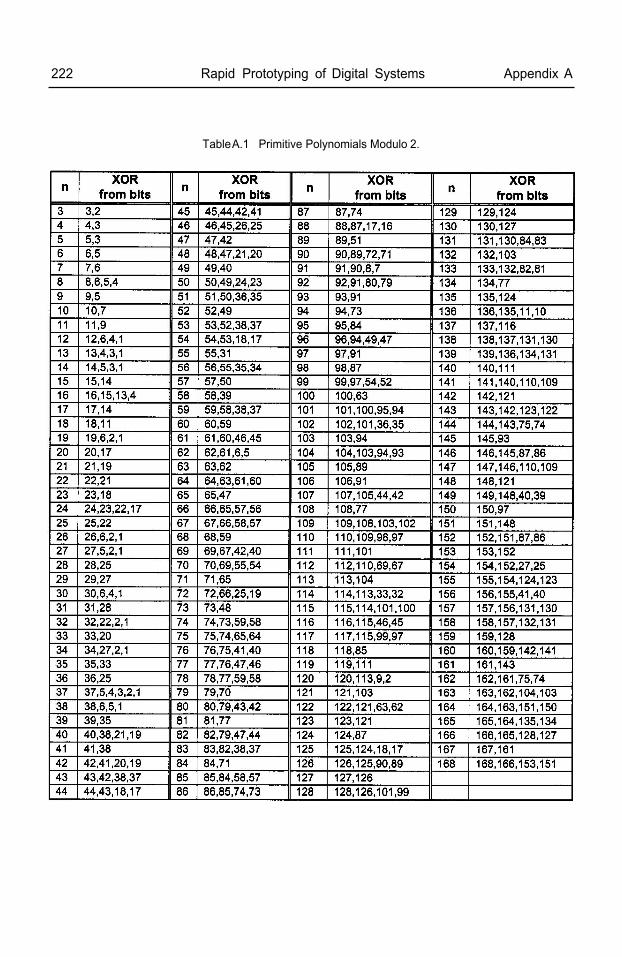
In many applications, random sequences of binary numbers are needed. These applications include random number generation for games, automatic test pattern generation, data encryption and decryption, data compression, and data error coding. Since a properly operating digital circuit never produces a random result, these sequences are called pseudo random. A long pseudo-randombinary sequence appears to be random at first glance. Table A.1 shows how to make an “n” bit pseudo-random binary sequence generator. Here is how it works for n = 8. Build an 8-bit shift register that shifts left one bit per clock cycle. Find the entry in Table A.l for n = 8. This entry shows that bits 8, 6, 5, 4 should all XORed or XNORed together to generate the next shift input used as the low bit in the shift register. Recall that the order of XOR operations does not matter. Note that the low-bit number is "1" and not "0" in this table. A state machine that is actually a non-binary counter is produced. The counter visits all 2n-1 non-zero states once in a pseudo-random order and then repeats. Since the counter visits every state once a uniform distribution of numbers from 1 to 2n-1 is generated. In addition to a shift register, only a minimal number of XOR or XNOR gates are needed for the circuit. The circuit is easy to synthesize in a HDL such as VHDL since only a few lines are required to shift and XOR the appropriate bits. Note that the next value in the random sequence is actually 2x or 2x + 1 the previous value, x. For applications that may require a more truly random appearing sequence order, use a larger random sequence generator and select a disjoint subset of the bits and shuffle the output bits. The initial value loaded in the counter is called the seed. The seed or the random number is never zero in this circuit. If a seed of zero is ever loaded in the shift register it will stay stuck at zero. If needed, the circuit can be modified so that it generates 2n states. For the same initial seed value, the circuit will always generate the same sequence of numbers. In applications that wait for input, a random seed can be obtained by building a counter with a fast clock and saving the value of the counter for the seed when an input device such as a pushbutton is activated. Additional information on pseudo-random binary sequence generators can be found in HDL Chip Design by D.J. Smith, Doone Publications, 1996, and Xilinx Application Note 52, 1996.
222 Rapid Prototyping of Digital Systems Appendix A
Table A.1 Primitive Polynomials Modulo 2.

Rapid Prototyping of Digital Systems Appendix B 223
Appendix B: MAX+PLUS II Design and Data File Extensions
Design Files Altera Design File (*.adf) EDIF Input File (*.edf) Graphic Design File (*.gdf) OrCAD Schematic File (*.sch) State Machine File (*.smf) Text Design File (*.tdf) Verilog Design File (*.v) VHDL Design File (*.vhd) Waveform Design File (*.wdf) Xilinx Netlist File (*.xnf)
Text Design Output File (*.tdo) Timing Anlyzer Output File (*.tao) Vector File (*.vec) VHDL Memory Model Output File (*.vmo)
Non-Editable Ancillary File Types
Compiler Netlist File (*.cnf) Hierarchy Interconnect File (*.hif) JEDEC file (*.jed) Node Database File (*.ndb) Programmer Object File (*.pof) Raw Binary File (*.rbf) Serial Bitstream File (*.sbf) Simulator Initialization File (*.sif) Simulator Netlist File (*.snf) SRAM Object File (*.sof)
Ancillary Data Files Assignment and Configuration File (*.acf) Assignment and Configuration Output (* .aco) Command File (*.cmd) EDIF Command File (*.edc) Fit File (*.fit) Intel Hexadecimal Format File (*.hex) History File (*.hst) Include File (*.inc) JTAG chain file (*.jcf) Library Mapping File (*.lmf) Log File (*.log) Memory Initialization File (*.mif) Memory Initialization Output File (*.mio) Message Text File (*.mtf) Programmer Log File (*.plf) Report File (*.rpt) Simulator Channel File (*.scf) Standard Delay Format (*.sdf) Standard Delay Format Output File (*.sdo) Symbol File (*.sym) Table File (*.tbl) Tabular Text File (*.ttf) Text Design Export File (*.tdx)
Rapid Prototyping of Digital Systems Appendix C 225
Appendix C: UP 1 Pin Assignments
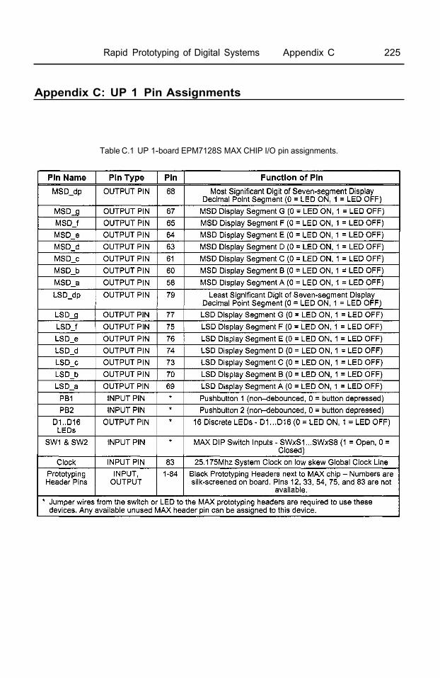
Table C.1 UP 1-board EPM7128S MAX CHIP I/O pin assignments.
226 Rapid Prototyping of Digital Systems Appendix C
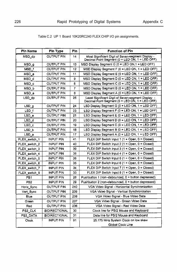
Table C.2 UP 1 Board 10K20RC240 FLEX CHIP I/O pin assignments.
Rapid Prototyping of Digital Systems Appendix C 227
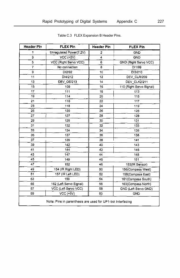
Table C.3 FLEX Expansion B Header Pins.

228 Rapid Prototyping of Digital Systems Glossary
Glossary
Assignment & Configuration File (.acf): An ASCII file (with the extension .acf) used by MAX+PLUS to store information about probe, pin, location, chip, clique, logic option, timing, connected pin and device assignments, as well as configuration settings for the Compiler, Simulator, and Timing Analyzer for an entire project. The ACF stores information entered with menu commands in all MAX+PLUS II applications. You can also edit an ACF manually in a Text Editor window. Active-high (Active-low) node: A node that is activated when it is assigned a value one (zero) or Vcc (Gnd). AHDL: Acronym for Altera Hardware Description Language. Design entry language that supports Boolean equation, state machine, conditional, and decode logic. It also provides access to all Altera and user-defined macrofunctions. Ancillary file: A file that is associated with a MAX+PLUS II project, but is not a design file in the project hierarchy tree. Antifuse: Any of the programmable interconnect technologies forming electrical connection between two circuit points rather than making open connections. Architecture: Describes the behavior, RTL or dataflow, and/ or structure of a VHDL entity. An architecture is created with an architecture body. A single entity can have more than one architecture. In some VHDL tools, configuration declarations are used to specify which architectures to use for each entity. Array: A collection of one or more elements of the same type that are accessed using one or more indices depending on dimension of array. Array data types are declared with an array range and array element type. ASIC: Acronym for Application-Specific Integrated Circuit. A circuit whose final photographic mask process is user design dependent. ASM: Acronym for Algorithmic State Machine Chart. A flow-chart based method used to represent a state diagram. Assert: A statement that checks whether a specified condition is true. If the condition is not true, a report is generated during simulation. Assignment: In VHDL, assignment refers to the transfer of a value to a symbolic name or group, usually through a Boolean equation. The value on the right side of an assignment statement is assigned to the symbolic name or group on the left. Asynchronous input: An input signal that is not synchronized to the device Clock. Attribute: A special identifier used to return or specify information about a named entity. Predefined attributes are prefixed with the ‘ character.Back annotation: Process of incorporating time delay values into a design netlist reflecting the interconnect capacitance obtained from a completed design. Also, in Altera's case, the process of copying device and resource assignments made by the Compiler into the Assignment and Configuration File for a project. This process preserves the current fit in future compilations. Block: A feature that allows partitioning of the design description within an architecture.Buried node: A combinatorial or registered signal that does not drive an output pin. Cell: A logic function. It may be a gate, a flip-flop, or some other structure. Usually, a cell is small compared to other circuit building blocks.
Rapid Prototyping of Digital Systems Glossary 229
Cell library: The collective name for a set of logic functions defined by the manufacturer of an FPLD or ASIC. Simulation and synthesis tools use cell libraries when simulating and synthesizing a model. CLB: Acronym for Configurable Logic Block. This element is the basic building block of the Xilinx FPGA product family. Clock: A signal that triggers registers. In a flip-flop or state machine, the clock is an edge-sensitive signal. In edge-triggered flip-flops, the output of the flip-flop can change only on the clock edge. Clock enable: The level-sensitive signal on a flip-flop with E suffix, e.g., DFFE. When the Clock enable is low, clock transitions on the clock input of the flip-flop are ignored.Compiler Netlist File (.cnf): A binary file (with the extension .cnf) that contains the data from a design file. The CNF is created by the Compiler Netlist Extractor module of the MAX+PLUS II Compiler. Component: Specifies the port of a primitive or macrofunction in VHDL. A component consists of the name of the primitive or macrofunction, and a list of its inputs and outputs. Components are specified in the Component declaration. Component instantiation: A concurrent statement that references a declared component and creates one unique instance of that component. Configuration EPROM: A serial EPROM designed to configure (program) a CPLD. Concurrent statements: HDL statements that are executed in parallel. Configuration: It maps instances of VHDL components to design entities and describes how design entities are combined to form a complete design. Configuration declarations are used to specify which architectures to use for each entity. Configuration scheme: The method used to load configuration (programming) data into an FPGA. Constant: An object that has a constant value and cannot be changed. Control unit: The hardware of a machine that controls the data path. CPLD: Acronym for complex programmable logic device. CPLDs include an array of functionally complete or universal logic cells with an interconnection network. Data Path: The hardware path that provides data processing and transfer of information in a machine, as opposed to the controller. Design entity: A file that contains description of the logic for a project and is compiled by the Compiler. Design library: Stores VHDL units that have already been compiled. These units can be referenced in VHDL designs. Design unit: A section of VHDL description that can be compiled separately. Each design unit must have a unique name within the project. Dual-purpose pins: Pins used to configure an FPLD device that can be used as I/O pins after initialization. Dynamic reconfigurability: Capability of an FPLD to change its function "on -the-fly"Embedded Array Block (EAB): A physically grouped set of 8 embedded cells that implement memory (RAM or ROM) or combinatorial logic in a FLEX 10K device. A single EAB can implement a memory block of 256 x 8, 512 x 4, 1,024 x 2, or 2,048 x 1 bits.

230 Rapid Prototyping of Digital Systems Glossary
EPLD: Acronym for EPROM programmable logic devices. This is a PLD that uses EPROM cells to internally configure the logic function. Also, erasable programmable logic device. Event: The change of value of a signal. Usually refers to simulation. Event scheduling: The process of scheduling of signal values to occur at some simulated time. Excitation function: A Boolean function that specifies logic that directs state transitions in a state machine. Exit condition: An expression that specifies a condition under which a loop should be terminated.FLEX 10K and FLEX 10KA: An Altera device family based on Flexible Logic Element MatriX architecture. This SRAM-based family offers high-performance,register-intensive, high-gate-count devices with embedded arrays. The FLEX 10K device family includes the EPF10K100, EPF10K70, EPF10K50, EPF10K40, EPF10K30, EPF10K20, and EPF10K10 devices. Fan-out: The number of output signals that can be driven by the output of a logic cell. Fast Track interconnect: Dedicated connection paths that span the entire width and height of a FLEX device. These connection paths allow the signals to travel between all LABS in device. Field name: An identifier that provides access to one element of a record data type. File type: A data type used to represent an arbitrary-length sequence of values of a given type. For loop: A loop construct in which an iteration scheme is a for statement. Finite state machine: The model of a sequential circuit that cycles through a predefined sequence of states. Fitting: Process of making a design fit into a specific FPLD architecture. Fitting involves technology mapping, placement, optimization, and partitioning among other operations.Flip-flop: An edge-sensitive memory device (cell) that stores a single bit of data. Floorplan: Physical arrangement of functions within a connection framework of signal routing channels. FPGA: Acronym for field programmable gate array. A regular array of logic cells that is either functionally complete or universal with an interconnection network of signal routing channels. FPLD: Acronym for field programmable logic device. An integrated circuit used for implementing digital hardware that allows the end user to configure the chip to realize different designs. Configuring such a device is done using either a special programming unit or by doing it " in system". FLPDs include both CPLDs and FPGAs.Functional prototype: Specifies the ports of a primitive or macrofunction in AHDL. It consists of the name of the primitive or macrofunction, and a list of its inputs and outputs in exact order in which they are used. An instance of the primitive or macrofunction can be inserted with an Instance declaration or an in line reference. Functional simulation: A simulation mode that simulates the logical performance of a project without timing information. Functional test vector: The input stimulus used during simulation to verity a VHDL model operates functionally as intended.

Rapid Prototyping of Digital Systems Glossary 23 1
Functionally complete: Property of some Boolean logic functions permitting them to make any logic function by using only that function. The properties include making the AND function with an invert or the OR function with an invert or the OR function with an invert. Fuse: A metallic interconnect point that can be electrically changed from short circuit to an open circuit by applying electrical current. Gate: An electronic structure, built from transistors that performs a basic logic function.Gate array: Array of transistors interconnected to form gates. The gates in turn are configured to form larger functions. Gated clock: A clock configuration in which the output of an AND or OR gate drives a clock. Generic: A parameter passed to a VHDL entity, component or block that describes additional, instance-specific information about that entity, component or block. Glitch or spike: A narrow output pulse that occurs when a logic level changes two or more times over a short period. Global signal: A signal from a dedicated input pin that does not pass through the logic array before performing its specified function. Clock, Preset, Clear, and Output Enable signals can be global signals. GND: A Low-level input voltage. It is the default inactive node value. Graphic Design File (.gdf): A schematic design file (with the extension .gdf) created with the MAX+PLUS II Graphic Editor. HDL: Acronym for Hardware Description Language. A special language used to describe digital hardware. Hexadecimal: The base 16 number system (radix). Hexadecimal digits are 0 through 9 and A through F. Hierarchy: The structure of a design description, expressed as a tree of related components.Identifier: A sequence of characters that uniquely identify a named entity in a design description.Index: A scalar value that specifies an element or range of elements within an array. Input vectors: Time-ordered binary numbers representing input values sequences to a simulation program. I/O cell register: A register on the periphery of a FLEX 8000 device or a fast input-type logic cell that is associated with an I/O pin. IP core: An intellectual property (IP) core is a previously developed synthesizable hardware design that provides a widely used function. Commercially licensed IP cores include functions such as microprocessors, microcontrollers, bus interfaces, multimedia and DSP operations, and communications controllers. LAB: Acronym for Logic Array Block. The LAB is the basic building block of the Altera MAX family. Each LAB contains at least one macrocell, an I/O block, and an expander product term array. Latch: A level-sensitive clocked memory device (cell) that stores a single bit of data. A High to low transition on the Latch Enable signal fixes the contents of the latch at the value of the data input until the next Low-to-High transition on Latch Enable. Latch enable: A level-sensitive signal that controls a latch. When it is High, the input flows through the output; when it is Low, the output holds its last value.
232 Rapid Prototyping of Digital Systems Glossary
Library: In VHDL a library statement is used to store analyzed design units. Literal: A value that can be applied to an object to some type. Logic Synthesizer: The Compiler module that uses several algorithms to minimize gate count, remove redundant logic, and utilize the device architecture as efficiently as possible. Processing can be customized with logic options and logic synthesis style assignments. This module also applies logic synthesis techniques to help implement timing requirements for a project. Least Significant Bit (LSB): The bit of a binary number that contributes the smallest quantity to the value of that number, i.e., the last member in a bus or group name. For example, the LSB for a bus or group named a[31 ..0] is a[0] (or a0). Logic Cell (LC): The generic term for a basic building block of an Altera device. In MAX devices, a logic cell (also called a macrocell) consists of two parts: combinatorial logic and a configurable register. The combinatorial logic allows a wide variety of logic functions. In FLEX 10K devices, a logic cell (also called a logic element) consists of a look-up table (LUT) and a programmable register to support sequential functions. Logic element: A basic building block of an Altera FLEX device. It consists of a look-up table i.e., a function generator that quickly computes any function of four variables, and a programmable flip-flop to support sequential functions. LPM: Acronym for library of Parameterized Modules. Denotes Altera’s library of design units that contain one or more changeable parts, and parameters that are used to customize a design unit as the application requires. Macro: When used with FPGAs, a logic cell configuration that can be repeated as needed. It can be a Hard or a Soft macro. Hard macros force predefined place and route rules between logic cells. Macrocell: In FPLDs, a portion of the FPLD that is smallest indivisible building block, In MAX devices it consists of two parts: combinatorial logic and a configurable register.MAX: Acronym for Multiple Array MatriX, which is an Altera product family. It is usually considered to be a CPLD. MAX+PLUS 11: Acronym for multiple array matrix programmable logic user system 11. A set of computer aided design (CAD) tools that allow design and implementation of custom logic circuits with Altera’s MAX and FLEX CPLD devices. Memory Initialization File (.mif): An ASCII file (with the extension .mif) used by MAX+PLUS II to specify the initial content of a memory block (RAM or ROM), i.e., the initial data values for each memory address. This file is used during project compilation and/or simulation. Mealy state machine: A type of state machine in which the outputs are a function of the inputs and the current state. Moore state machine: A state machine in which the present state depends only on its previous input and previous state, and the present output depends only on the present state. In general Moore states machines have more states than a Mealy machine. Most Significant Bit (MSB): The bit of a binary number that contributes the greatest quantity to the value of that number, and the first member in a bus or group name. For example, the MSB for a bus named a[31..0] is a[31]. Mode: A direction of signal (either in, out, inout or buffer) used as subprogram parameter or port.
Rapid Prototyping of Digital Systems Glossary 233
Model: A representation that behaves similarly to the operation of some digital circuit.MPLD: Acronym for Mask Programmed Logic Device. Netlist: A text file that describes a logic design. Minimal requirements are identification of function elements, inputs, outputs, and connections. Netist synthesis: Process of deriving a netlist from an abstract representation, usually from a hardware description language. NRE: Acronym for Non-Recurring Engineering expense. It reefers to one-time charge covering the use of design facilities, masks and overhead for test development of ASICs.Object: A named entity of a specific type that can be assigned a value. Object in VHDL include signals, constants, variables and files. Octal: The base 8 number system (radix). Octal digits are 0 though 7. One Hot Encoding: A design technique used more with FPGAs than CPLDs. Only one flip-flop output is active at any time. One flip-flop per state is used. State outputs do not need to be decoded and they are hazard free. Package: A collection of commonly used VHDL constructs that can be shared by more than one design unit. PAL: Acronym for programmable array logic. A relatively small FPLD containing a programmable AND plane followed by a fixed-OR plane. Parameter: An object or literal passed into a subprogram via that subprogram's parameter list. Partitioning: Setting boundaries between subsections of a system or between multiple FPLD devices. Physical types: A data type used to represent measurements. Pin Number: A number used to assign an input or output signal in a design file, which corresponds to the pin number on an actual device. PLA: (programmable logic array) a relatively small FPLD that contains two levels of programmable logic-an AND plane and an OR plane. Placement: Physical assignment of a logical function to a specific location within an FPGA. Once the logic function is placed, its interconnection is made by routing. PLD: Acronym for programmable logic device. This class of devices comprise PALS,PLAs, FPGAs, and CPLDs. Port: A symbolic name that represents an input or output of a primitive or of a macrofunction design file. Primitive: One of the basic functional blocks used to design circuits with MAX+PLUS II software. Primitives include buffers, flip-flops, latch, logical operators, ports, etc. Process: A basic VHDL concurrent statement represented by a collection of sequential statements that are executed whenever there is an event on any signal that appears in the process sensitivity list, or whenever an event occurs that satisfies condition of a wait statement within the process. Product Term: Two or more factors in a Boolean expression combined with an AND operator constitute a product term, where "product" means "logic product."Programmable switch: A user programmable switch that can connect a logic element or input/output element to an interconnect wire or one interconnect wire to another.
234 Rapid Prototyping of Digital Systems Glossary
Project: A project consists of all files that are associated with a particular design, including all subdesign files and ancillary files created by the user or by MAX+PLUS II software. The project name is the same as the name of the top-level design file without an extension. Propagation delay: The time required for any signal transition to travel between pins and/or nodes in a device. Radix: A number base. Group logic level and numerical values are entered and displayed in binary, decimal, hexadecimal, or octal radix in MAX+PLUS II. Reset: An active-high input signal that asynchronously resets the output of a register to a logic Low (0) or a state machine to its initial state, regardless of other inputs. Range: A subset of the possible values of a scalar type. Register: A memory device that contains several latches or flip-flops that are clocked from the same clock signal. Resource: A resource is a portion of a device that performs a specific, user-definedtask (e.g., pins, logic cells, interconnection network). Retargetting: A process of translating a design from one FPGA or other technology to another. Retargetting involves technology-mapping optimization. Reset: An active-high input signal that asynchronously resets the output of a register to a logic Low (0) or a state machine to its initial state, regardless of other inputs. Ripple Clock: A clocking scheme in which the Q output of one flip-flop drives the Clock input to another flip-flop. Ripple clocks can cause timing problems in complex designs.RTL: Acronym for Register Transfer Level. The model of circuit described in VHDL that infers memory devices to store results of processing or data transfers. Sometimes it is referred to as a dataflow-style model. Scalar: A data type that has a distinct order of its values, allowing two objects or literals of that type to be compared using relational operators. Semicustom: General category of integrated circuits that can be configured directly by the user of an IC. It includes gate arrays and FPLD devices. Signal: In VHDL a data object that has a current value and scheduled future values at simulation times. In RTL models signals denote direct hardware connections. Simulation: Process of modeling a logical design and its stimuli in which the simulator calculates output signal values. Slew rate: Time rate of change of voltage. Some FPGAs permit a fast or slow slew rate to be programmed for an output pin. Slice: A one-dimensional, contiguous array created as a result of constraining a larger one-dimensional array. Speed performance: The maximum speed of a circuit implemented in an FPLD. It is set by the longest delay through any for combinational circuits, and by maximum clock frequency at which the circuit operates properly for sequential circuits. State transition diagram: A graphical representation of the operation of a finite state machine using directed graphs. State: A state is implemented in a device as a pattern of 1's and 0's (bits) that are the outputs of multiple flip-flops (collectively called a state machine state register). Structural-type architecture: The level at which VHDL describes a circuit as an arrangement of interconnected components. Subprogram: A function or procedure. It can be declared globally or locally.
Rapid Prototyping of Digital Systems Glossary 235
Sum-of-products: A Boolean expression is said to be in sum-of-products form if it consists of product terms combined with the OR operator. Synthesis: The process of converting the model of a design described in VHDL from one level of abstraction to another, lower and more detailed level that can be implemented in hardware. Technology mapping: Process of translating the function of a design from one technology to another. All versions of the design would have the same function, but the logic cells used would be very different. Test bench: A VHDL model used to verify the correct behavior of another VHDL model, commonly known as the unit under test. Tri-state Buffer: A buffer with an input, output, and controlling Output Enable signal. If the Output Enable input is High, the output signal equals the input. If the Output Enable input is Low, the output signal is in a state of high impedance. Tri-stateoutputs can be tied together but only one should ever be enabled at any given time. Timing Simulation: A simulation that includes the actual device delay times. Two's Complement: A system of representing binary numbers in which the negative of a number is equal to its logic inverse plus 1. In VHDL, you must declare a two's complement binary number with a signed data type or use the signed library. Type: A declared name and its corresponding set of declared values representing the possible values the type. Type declaration: A VHDL declaration statement that creates a new data type. A type declaration must include a type name and a description of the entire set of possible values for that type. Universal logic cell: A logic cell capable of forming any combinational logic function of the number of inputs to the cell. RAM, ROM and multiplexers have been used to form universal logic cells. Sometimes they are also called look-up tables or function generators.Usable gates: Term used to denote the fact that not all gates on an FPGA may be accessible and used for application purposes. Variable: In VHDL, a data object that has only current value that can be changed in variable assignment statement. Verilog: An HDL with features similar to VHDL with a syntax reminiscent of C. VCC: A high-level input voltage represented as a High (1) logic level in binary group values.VHDL: Acronym for VHSIC (Very High Speed Integrated Circuits) Hardware Description Language. VHDL is used to describe function, interconnect and modeling. VITAL: Acronym for VHDL Initiative Toward ASIC Libraries. An industry-standardformat for VHDL simulation libraries.

Indexfor loop, 208
Altera FLEX 10K Architecture, 42 embedded array blocks (EABs), 44 Input output elements (IOEs), 46 logic array block (LAB), 44
Altera FLEX 10K70 CPLD, 41,215 Altera MAX 7000s Architecture, 41 antifuse, 49 application specific integrated circuits (ASICs), 38arithmetic logic unit (ALU), 87
gate arrays, 38
hardware emulator, 49
if statement, 81
case statement, 79 cathode ray tube (CRT), 134 clock edge, 82 clocking in VHDL, 82 color in video display, 134 complex programmable logic devices (CPLDs), 38 component, 94 computer aided design (CAD) tools, 48 concurrent assignment statement, 79 conv_integer, 78 conv_std_logic_vector, 78
JTAG. See UP 1 JTAG setup
keyboard. See PS/2 keyboard
look-up table (LUT), 43 LPM_DIV, 88 LPM_MULT, 88 LPM_RAM_DQ, 92
digital oscilloscope, 57 LPM_ROM, 143 dithering, 149
macrocell, 41 MAX PLUS II electric train
assigning a device, 6 assigning pins, 7 assignment and configuration file (*.acf), 9, 17, 21buses, 55 compilation, 9 connecting signal lines, 7 entering pin names, 8 errors and warnings, 10 file extensions, 223 floorplan editor, 23 graphic editor, 6 hierarchy, 54 report file (*.rpt), 10 schematic capture. See graphic editor simulation, 10 simulation test vectors or stimulus, 11 simulaton vector file (*.vec), 110
direction, 102 example controller, 104 I/O summary, 104 sensors, 103 simulation, 110 switches, 103 track power, 102 video output, 114
(EEPROM), 41 electrically erasable programmable read only memory
field programmable gate arrays (FPGAs), 38 field programmable logic devices (FPLDs)
floating point hardware, 89 applications, 48
238 Rapid Prototyping of Digital Systems
symbol editor, 24 battery, 185 symbol entry, 6 battery charger, 186 timing analysis, 22, 56 communication, 179 tutorial, 2, 52 expansion header, 188, 227 waveform editor file (*.scf), 11 infrared poximity detector, 177
line tracker sensor, 177 control, 203 magnetic compass, 181 decode, 208 modifying servos, 173 dmemory, 2 12 parts list, 185 execute, 210 sensors, 176
servo drive motors, 172 execution on UP 1, 214 hardware implementation, 197 sonar, 180 ifetch, 205 VHDL servo driver, 174 instruction formats, 196 instructions, 197 pipelined implementation, 198 simulation, 213 top-spim, 200 VHDL synthesis model, 199
mouse. See PS/2 mouse multiply and divide hardware, 88
MIPS, 196
run length encoding (RLE), 148
seven segment decoder, 79 shift operation in VHDL, 88 SR latch, 57 standard cells, 38
pin grid array package (PGA), 41 pixels, 134 plastic J-lead chip carrier (PLCC), 41 plastic quad flat pack (PQFP), 41 port map, 94 process, 79 process sensitivity list, 79, 82 processor fetch, decode and execute cycle, 122 unit under test (UUT), 94 programmable array logic (PALs), 39 UP 1, 4, 30 programmable interconnect array (PIA), 42 attaching power, 12 programmable logic, 38 downloading, 12 programmable logic arrays (PLAs), 39 FLEX 10K70 and 10K50 upgrade, 2 15 programmable logic devices, (PLDs), 39 FLEX device, 34 PS/2 keyboard, 154 FLEX I/O pins, 35, 188,226
communications protocol, 155 heat sink, 36 connections, 154 JTAG setup for downloading, 13 make and break codes, 155 jumper setup, 31 scan codes, 155 LEDs, 5 VHDL example, 161 longer cable, 36
MAX device, 31 commands and messages, 166 MAX I/O pins, 33, 225 data packet format, 167 Pin Assignments, 225 data packet processing, 169 PLCC extraction tool, 36 example design, 170 power supplies, 36 initialization, 168 pushbutton contact bounce, 58
pushbuttons, 4 UP1 computer, 120
fetch, decode, and execute, 122 reconfigurable computing, 49 instructions, 121
reduced instruction set computer (RISC), 196 VHDL model, 126
refresh. See VGA video display refresh UP1bot. See robotUP1core library, 64 robot, 172
assembly, 18 1 char_ROM, 71
testbench, 94to_stdlogicvector, 78train. See electric train
PS/2 mouse, 166
Rapid Prototyping of Digital Systems Index 239
clk_div, 58, 68 debounce, 58, 66 dec_7seg, 53, 65 inferred latches, 84 installation, 52 libraries, 76, 84 keyboard, 72, 161 operators, 77 mouse, 73, 168 shift operations, 77 onepulse, 67 standard logic (STD_LOGIC), 76 tutorial, 52 structural model, 92 vga_sync, 69,138 synthesis of a counter, 84
synthesis of a multiplexer, 81 synthesis of a state machine, 85
synthesis of an adder, 87 synthesis of an ALU, 87 synthesis of an incrementer, 84 synthesis of an subtractor, 87 synthesis of digital hardware, 78 synthesis of flip-flops and registers, 82 synthesis of gate networks, 78 synthesis of memory, 89 synthesis of multiply and divide hardware, 88 synthesis of seven segment decoder, 79 train state machine, 108 tutorial, 14 using templates for entry, 14, 18
video display. See VGA video display
errors and warnings, 17 hierarchy in models, 92
synthesis of a tri-state output, 82 Verilog
compilation, 21 Continuous Assignment Statement, 19 errors and warnings, 21 tutorial, 17
VGA video display, 134 bouncing ball example, 149 character based, 141 character font ROM, 144 color mixing using dithering, 149 data compression, 148 generation using a CPLD, 137 graphics display, 147 horizontal sync, 134 pin assignments, 140 refresh, 134 RGB signals, 134 using a final output register, 140 vertical sync, 134 video examples, 141
Architecture body, 15 compilation, 17 conversion of data types, 78 data types, 76 editor syntax coloring, 15, 19 Entity, 14, 18
wait statement, 82 with statement, 81
VHDL
Xilinx 4000 Architecture, 46 configurable logic block (CLB), 46 Input output blocks (IOBs), 48
Xilinx Virtex, 49

240 Rapid Prototyping of Digital Systems
About the Accompanying CD-ROM
Rapid Prototyping of Digital Systems, First Edition, includes a CD-ROM that contains both Altera's MAX+PLUS II Student Edition and all of the example designs from the text.
MAX+PLUS II Software The companion CD-ROM contains Altera's MAX+PLUS II Student Edition programmable logic development software. The MAX+PLUS II software is a fully integrated design environment that offers unmatched flexibility and performance. The intuitive graphical interface is complemented by complete and instantly accessible online documentation, which makes learning and using the MAX+PLUS II software quick and easy. The MAX+PLUS II version 9.23 Student Edition software offers the following features:
•
•
Operates on stand-alone PCs running Windows 95/98, and Windows NT 3.51 and 4.0
Design entry includes graphical and text-based, including VHDL, Verilog HDL, and the Altera Hardware Description Language (AHDL),
Design compilation for product-term and look-up table device architectures, with device support for members of the Altera® FLEX® 10K, FLEX 8000, FLEX 6000, MAX® 7000, and MAX 7000s device families
Design verification with full timing and functional simulation
•
•
Installing the MAX+PLUS II Software
Insert the MAX+PLUS II CD-ROM in your CD-ROM drive. In the Start menu, choose RUN and type CD-ROMdrive:\MP2_92SE.exe in the Command Line box. You are guided through the installation and the online registration procedure required to obtain an authorization code from Altera.
Design Examples from the Book
Design examples from the book are located in the CD-ROM directories, booksoft/chapx, where x is the chapter number. To use the design files, copy them to the hard disk drive to your max2work directory or a subdirectory. In addition to *.gdf and *.vhd design files, be sure to copy any *.acf, *.scf, or *.hif files for each project. The UP1core library files are in booksoft/chap5. Browse the file, index.htm, using a web browser on the CD-ROM for additional information.
This CD-ROM is distributed by Kluwer Academic Publishers with *ABSOLUTELY NO SUPPORT* and *NO WARRANTY* from Kluwer Academic Publishers.
Kluwer Academic Publishers and the authors shall not be liable for damages in connection with, or arising out of, the furnishing, performance or use of the CD-ROM.