application note 2072 lmh6522 evaluation...
TRANSCRIPT

LMH6522
Application Note 2072 LMH6522 Evaluation Board
Literature Number: SNOA552

LMH6522 Evaluation Board National SemiconductorApplication Note 2072Loren SiebertJuly 29, 2011
30127811
FIGURE 1. LMH6522EVAL Evaluation Board
General DescriptionThe LMH6522EVAL evaluation board is designed to aid in thecharacterization of National Semiconductor’s High SpeedLMH6522 Digital Controlled Variable Gain Amplifier (DVGA).
Use the evaluation board as a guide for high frequency layoutand as a tool to aid in device testing and characterization.
Basic OperationThe LMH6522 DVGA has differential inputs and differentialoutputs. The evaluation board has been designed to easilyinterface with 50Ω single ended test equipment. TheLMH6522EVAL evaluation board is shipped with input andoutput transformers installed to convert the DVGA differentialinputs and outputs to single ended signal paths. As built, thesignal path uses the IN+ and OUT− marked connectors. TheIN− and OUT+ signal paths are grounded. The signal pathsare fully symmetrical.
To preserve proper bias voltages there are DC blocking ca-pacitors on both the input and output signal traces. The input
pins of the LMH6522 will self bias to approximately mid supply(2.5V). The output pins need to be biased to near ground po-tential. Inductors are installed on the evaluation board toprovide proper output biasing. The bias current is approxi-mately 36 mA per output pin. Capacitors between the ampli-fier and the output transformer will prevent offset currentsfrom flowing through the transformer primary coil. Many trans-formers will show increased distortion products when there isa DC current flowing through the primary coil.
Transformers TINA– TIND can provide both impedancematching as well as single ended to differential conversion.The board is shipped with 2:1 impedance ratio transformers(1.4:1 Voltage ratio) that will match 50Ω equipment with the100Ω input impedance of the LMH6522 DVGA .
On the output side of the board are transformers TOUTA -TOUTD. The output transformers were chosen to provide agood compromise between distortion performance and phys-ical size. The LMH6522 is capable of driving a wide range ofload impedances. A 200 Ohm load impedance was chosenfor the evaluation board to emulate performance with a 100
SPI™ is a trademark of Motorola, Inc.
National Semiconductor® is a registered trademark of National Semiconductor Corporation.
© 2011 National Semiconductor Corporation 301278 www.national.com
LM
H6522 E
valu
atio
n B
oard
AN
-2072

Ohm back terminated filter. Other configurations are possiblewith minor rework of the evaluation board.
Capacitors CCOA+/− through CCOD+/− are installed to iso-late the DVGA outputs from the output transformer primarywindings. The output resistors are 40.2 Ohm matching resis-tors. The output impedance of the LMH6522 amplifier is verylow (10Ω @ 50MHz), and the 40.2 Ohm resistors provide ter-mination for the 100 Ohm load presented by the transformer
when the evaluation board is connected to 50 Ohm test equip-ment. The JTX–2–10T output transformers have a 1:2impedance ratio.
The LMH6522 DVGA is configured to have a maximum gainof 26dB. The transformers and matching resistors contributea loss of approximately 7.5 dB. Gain through the board shouldmeasure approximately 18.6 dB.
30127805
FIGURE 2. Output Schematic
30127806
FIGURE 3. Input Schematic
Zoomed in portions of the input and output schematics areshown above in Figure 2 and Figure 3. The these schematicsshow that the evaluation board, as shipped, has been builtwith single ended inputs and outputs. The full signal path
schematic is shown in Figure 10 and the full evaluation boardschematic, including the digital control portions is availablein .PDF format upon request.
www.national.com 2
AN
-2072

Using with Differential Sources or
LoadsThe LMH6522EVAL board was designed to be easily modi-fied by the customer for fully differential operation. To modifythe board for differential operation it is necessary to removethe transformers and the resistors that ground the unusedsignal paths. Next, add coupling capacitors on the IN- andOUT+ signal lines, and finally place shorting jumpers acrossthe appropriate transformer pads. At this point theLMH6522EVAL board will be configured for a 100 Ohm dif-ferential signal path.
Other load conditions can also be easily matched by placingappropriate components on existing pads on the evaluationboard. When changing components remember to keep theinput path AC coupled so that the input common mode voltageis preserved.
Gain ControlFor ease of use, banks of DIP switches are set up to controlgain settings. For high speed interfacing to a logic analyzerthere are also 0.1” header strips. The pin functions for theseheaders are shown in the table below. For detailed instruc-tions on the pin functions see the LMH6522 productdatasheet.
The dip switches settings will impact the on-board impedancefor the J1 header pins. With the dip switches should be set tothe OPEN position the header pins are unterminated. Whenthe dip switches are closed the header pins are terminatedwith 49.9 Ohm resistors. This would be the preferred settingfor most high speed signal interfaces. Refer to the productdatasheet for the absolute maximum voltage and current rat-ings of the digital pins.
Header Jack Pin Assignments(CONA. CONB, CONC, COND)(Pin 1 is pin closest to inputconnectors)Header Pin Parallel Function
1 Address bit 0
2 Address bit 1
3 Address bit 2
4 Address bit 3
Header Pin Parallel Function
5 Address bit 4
6 Ground
7 Enable (Tri State Pin)
SPI™Compatible Gain Control
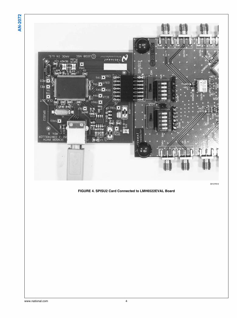
using the SPISU2 CardThe LMH6522_EVAL board can easily be controlled in theserial mode using National Semiconductor®'s SPISU2 USBto SPI controller card. This card and the required software areavailable on the National Semiconductor website. Directionsfor installing the USB control software and evaluation boarddrivers are in the user's guide available on the National Semi-conductor website.
To use the SPI card, the LMH6522 DVGA must be put intoserial mode. This is done by placing a shorting block on theMODE jumper pins which are located near the power con-nectors in the center of the board. Once this shorting block isin place the switches on the SWA switch block all need to beput in the OFF position. If the switches are in the ON positionthe digital lines will be grounded and the SPISU2 card will notbe able to communicate with the DVGA.
Once the SPUSI2 board drivers and TinyI2CSPI software areinstalled, connect the SPUSI2 board directly onto theLMH6522_EVAL double-row header (J1) by aligning pin 1 asshown in Figure 4. Plug the USB cable into the SPISU2 cardand the host PC. Start the TinyI2CSPI software and load theLMH6522 profile as shown in Figure 5. Additional commandscan be generated by changing the data in the MOSI column.Check the LMH6522 datasheet for details on the data to besent to the DVGA registers. The example SPI commands area good starting point for generating the desired commands.
SPISU2 Header Pins Serial Function
1 Chip Select
2 Ground
3 Clock
4 N/A
5 Serial Data Out (MISO)
6 N/A
7 Serial Data IN (MOSI)
8 — 14 N/A
3 www.national.com
AN
-2072
30127812
FIGURE 4. SPISU2 Card Connected to LMH6522EVAL Board
www.national.com 4
AN
-2072

30127813
FIGURE 5. TinyI2CSPI Settings
Board LayoutThe LMH6522EVAL board has been designed to provide ex-cellent signal integrity and has been thermally enhanced toprovide for excellent heat dissipation. The LMH6522EVALboard has balanced differential signal traces as well as pro-vision for using single ended test equipment.
The LMH6522 DVGA dissipates approximately 2.4W of pow-er. To keep the amplifier cool the LMH6522EVAL board uses8 layers of copper, many of which are solid gound planesconnected directly to the LMH6522 exposed thermal pad.This provides excellent heat dissipation and eliminates theneed for a heat sink. The board design files (in GERBER)format are available upon request.
5 www.national.com
AN
-2072

30127803
FIGURE 6. Evaluation Board Top Layer
30127814
FIGURE 7. Layout Layer 2. Showing Metal Removed from under Input and Output Pins.
www.national.com 6
AN
-2072

30127804
FIGURE 8. Evaluation Board Bottom Layer
30127810
FIGURE 9. Logic Header Schematic
7 www.national.com
AN
-2072

30127807
FIG
UR
E 1
0.
Sig
na
l P
ath
Sc
he
ma
tic
www.national.com 8
AN
-2072

Additional Design ToolsThe RD-179: High-IF Sub-sampling Receiver Subsysemboard (SP16160CH1RB) is also available. This reference de-sign includes the ADC16DV160 ADC, the LMH6517 DVGA,
and the LMK04031B precision clock conditioner. Power reg-ulation, filters and controlled impedance board layout are allprovided in this reference design. Please visit the NationalSemiconductor website for further details.
9 www.national.com
AN
-2072

NotesA
N-2
072
LM
H6522 E
valu
ati
on
Bo
ard
For more National Semiconductor product information and proven design tools, visit the following Web sites at:
www.national.com
Products Design Support
Amplifiers www.national.com/amplifiers WEBENCH® Tools www.national.com/webench
Audio www.national.com/audio App Notes www.national.com/appnotes
Clock and Timing www.national.com/timing Reference Designs www.national.com/refdesigns
Data Converters www.national.com/adc Samples www.national.com/samples
Interface www.national.com/interface Eval Boards www.national.com/evalboards
LVDS www.national.com/lvds Packaging www.national.com/packaging
Power Management www.national.com/power Green Compliance www.national.com/quality/green
Switching Regulators www.national.com/switchers Distributors www.national.com/contacts
LDOs www.national.com/ldo Quality and Reliability www.national.com/quality
LED Lighting www.national.com/led Feedback/Support www.national.com/feedback
Voltage References www.national.com/vref Design Made Easy www.national.com/easy
PowerWise® Solutions www.national.com/powerwise Applications & Markets www.national.com/solutions
Serial Digital Interface (SDI) www.national.com/sdi Mil/Aero www.national.com/milaero
Temperature Sensors www.national.com/tempsensors SolarMagic™ www.national.com/solarmagic
PLL/VCO www.national.com/wireless PowerWise® DesignUniversity
www.national.com/training
THE CONTENTS OF THIS DOCUMENT ARE PROVIDED IN CONNECTION WITH NATIONAL SEMICONDUCTOR CORPORATION(“NATIONAL”) PRODUCTS. NATIONAL MAKES NO REPRESENTATIONS OR WARRANTIES WITH RESPECT TO THE ACCURACYOR COMPLETENESS OF THE CONTENTS OF THIS PUBLICATION AND RESERVES THE RIGHT TO MAKE CHANGES TOSPECIFICATIONS AND PRODUCT DESCRIPTIONS AT ANY TIME WITHOUT NOTICE. NO LICENSE, WHETHER EXPRESS,IMPLIED, ARISING BY ESTOPPEL OR OTHERWISE, TO ANY INTELLECTUAL PROPERTY RIGHTS IS GRANTED BY THISDOCUMENT.
TESTING AND OTHER QUALITY CONTROLS ARE USED TO THE EXTENT NATIONAL DEEMS NECESSARY TO SUPPORTNATIONAL’S PRODUCT WARRANTY. EXCEPT WHERE MANDATED BY GOVERNMENT REQUIREMENTS, TESTING OF ALLPARAMETERS OF EACH PRODUCT IS NOT NECESSARILY PERFORMED. NATIONAL ASSUMES NO LIABILITY FORAPPLICATIONS ASSISTANCE OR BUYER PRODUCT DESIGN. BUYERS ARE RESPONSIBLE FOR THEIR PRODUCTS ANDAPPLICATIONS USING NATIONAL COMPONENTS. PRIOR TO USING OR DISTRIBUTING ANY PRODUCTS THAT INCLUDENATIONAL COMPONENTS, BUYERS SHOULD PROVIDE ADEQUATE DESIGN, TESTING AND OPERATING SAFEGUARDS.
EXCEPT AS PROVIDED IN NATIONAL’S TERMS AND CONDITIONS OF SALE FOR SUCH PRODUCTS, NATIONAL ASSUMES NOLIABILITY WHATSOEVER, AND NATIONAL DISCLAIMS ANY EXPRESS OR IMPLIED WARRANTY RELATING TO THE SALEAND/OR USE OF NATIONAL PRODUCTS INCLUDING LIABILITY OR WARRANTIES RELATING TO FITNESS FOR A PARTICULARPURPOSE, MERCHANTABILITY, OR INFRINGEMENT OF ANY PATENT, COPYRIGHT OR OTHER INTELLECTUAL PROPERTYRIGHT.
LIFE SUPPORT POLICY
NATIONAL’S PRODUCTS ARE NOT AUTHORIZED FOR USE AS CRITICAL COMPONENTS IN LIFE SUPPORT DEVICES ORSYSTEMS WITHOUT THE EXPRESS PRIOR WRITTEN APPROVAL OF THE CHIEF EXECUTIVE OFFICER AND GENERALCOUNSEL OF NATIONAL SEMICONDUCTOR CORPORATION. As used herein:
Life support devices or systems are devices which (a) are intended for surgical implant into the body, or (b) support or sustain life andwhose failure to perform when properly used in accordance with instructions for use provided in the labeling can be reasonably expectedto result in a significant injury to the user. A critical component is any component in a life support device or system whose failure to performcan be reasonably expected to cause the failure of the life support device or system or to affect its safety or effectiveness.
National Semiconductor and the National Semiconductor logo are registered trademarks of National Semiconductor Corporation. All otherbrand or product names may be trademarks or registered trademarks of their respective holders.
Copyright© 2011 National Semiconductor Corporation
For the most current product information visit us at www.national.com
National SemiconductorAmericas TechnicalSupport CenterEmail: [email protected]: 1-800-272-9959
National Semiconductor EuropeTechnical Support CenterEmail: [email protected]
National Semiconductor AsiaPacific Technical Support CenterEmail: [email protected]
National Semiconductor JapanTechnical Support CenterEmail: [email protected]
www.national.com
IMPORTANT NOTICE
Texas Instruments Incorporated and its subsidiaries (TI) reserve the right to make corrections, modifications, enhancements, improvements,and other changes to its products and services at any time and to discontinue any product or service without notice. Customers shouldobtain the latest relevant information before placing orders and should verify that such information is current and complete. All products aresold subject to TI’s terms and conditions of sale supplied at the time of order acknowledgment.
TI warrants performance of its hardware products to the specifications applicable at the time of sale in accordance with TI’s standardwarranty. Testing and other quality control techniques are used to the extent TI deems necessary to support this warranty. Except wheremandated by government requirements, testing of all parameters of each product is not necessarily performed.
TI assumes no liability for applications assistance or customer product design. Customers are responsible for their products andapplications using TI components. To minimize the risks associated with customer products and applications, customers should provideadequate design and operating safeguards.
TI does not warrant or represent that any license, either express or implied, is granted under any TI patent right, copyright, mask work right,or other TI intellectual property right relating to any combination, machine, or process in which TI products or services are used. Informationpublished by TI regarding third-party products or services does not constitute a license from TI to use such products or services or awarranty or endorsement thereof. Use of such information may require a license from a third party under the patents or other intellectualproperty of the third party, or a license from TI under the patents or other intellectual property of TI.
Reproduction of TI information in TI data books or data sheets is permissible only if reproduction is without alteration and is accompaniedby all associated warranties, conditions, limitations, and notices. Reproduction of this information with alteration is an unfair and deceptivebusiness practice. TI is not responsible or liable for such altered documentation. Information of third parties may be subject to additionalrestrictions.
Resale of TI products or services with statements different from or beyond the parameters stated by TI for that product or service voids allexpress and any implied warranties for the associated TI product or service and is an unfair and deceptive business practice. TI is notresponsible or liable for any such statements.
TI products are not authorized for use in safety-critical applications (such as life support) where a failure of the TI product would reasonablybe expected to cause severe personal injury or death, unless officers of the parties have executed an agreement specifically governingsuch use. Buyers represent that they have all necessary expertise in the safety and regulatory ramifications of their applications, andacknowledge and agree that they are solely responsible for all legal, regulatory and safety-related requirements concerning their productsand any use of TI products in such safety-critical applications, notwithstanding any applications-related information or support that may beprovided by TI. Further, Buyers must fully indemnify TI and its representatives against any damages arising out of the use of TI products insuch safety-critical applications.
TI products are neither designed nor intended for use in military/aerospace applications or environments unless the TI products arespecifically designated by TI as military-grade or "enhanced plastic." Only products designated by TI as military-grade meet militaryspecifications. Buyers acknowledge and agree that any such use of TI products which TI has not designated as military-grade is solely atthe Buyer's risk, and that they are solely responsible for compliance with all legal and regulatory requirements in connection with such use.
TI products are neither designed nor intended for use in automotive applications or environments unless the specific TI products aredesignated by TI as compliant with ISO/TS 16949 requirements. Buyers acknowledge and agree that, if they use any non-designatedproducts in automotive applications, TI will not be responsible for any failure to meet such requirements.
Following are URLs where you can obtain information on other Texas Instruments products and application solutions:
Products Applications
Audio www.ti.com/audio Communications and Telecom www.ti.com/communications
Amplifiers amplifier.ti.com Computers and Peripherals www.ti.com/computers
Data Converters dataconverter.ti.com Consumer Electronics www.ti.com/consumer-apps
DLP® Products www.dlp.com Energy and Lighting www.ti.com/energy
DSP dsp.ti.com Industrial www.ti.com/industrial
Clocks and Timers www.ti.com/clocks Medical www.ti.com/medical
Interface interface.ti.com Security www.ti.com/security
Logic logic.ti.com Space, Avionics and Defense www.ti.com/space-avionics-defense
Power Mgmt power.ti.com Transportation and Automotive www.ti.com/automotive
Microcontrollers microcontroller.ti.com Video and Imaging www.ti.com/video
RFID www.ti-rfid.com
OMAP Mobile Processors www.ti.com/omap
Wireless Connectivity www.ti.com/wirelessconnectivity
TI E2E Community Home Page e2e.ti.com
Mailing Address: Texas Instruments, Post Office Box 655303, Dallas, Texas 75265Copyright © 2011, Texas Instruments Incorporated