application note 28 thermocouple measurement · temperature is easily the most commonly measured...
TRANSCRIPT
Application Note 28
AN28-1
an28f
February 1988
Thermocouple MeasurementJim Williams
Introduction
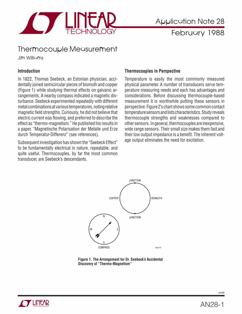
In 1822, Thomas Seebeck, an Estonian physician, acci-dentally joined semicircular pieces of bismuth and copper (Figure 1) while studying thermal effects on galvanic ar-rangements. A nearby compass indicated a magnetic dis-turbance. Seebeck experimented repeatedly with different metal combinations at various temperatures, noting relative magnetic fi eld strengths. Curiously, he did not believe that electric current was fl owing, and preferred to describe the effect as “thermo-magnetism.” He published his results in a paper, “Magnetische Polarisation der Metalle und Erze durch Temperatur-Differenz” (see references).
Subsequent investigation has shown the “Seebeck Effect” to be fundamentally electrical in nature, repeatable, and quite useful. Thermocouples, by far the most common transducer, are Seebeck’s descendants.
Thermocouples in Perspective
Temperature is easily the most commonly measured physical parameter. A number of transducers serve tem-perature measuring needs and each has advantages and considerations. Before discussing thermocouple-based measurement it is worthwhile putting these sensors in perspective. Figure 2’s chart shows some common contact temperature sensors and lists characteristics. Study reveals thermocouple strengths and weaknesses compared to other sensors. In general, thermocouples are inexpensive, wide range sensors. Their small size makes them fast and their low output impedance is a benefi t. The inherent volt-age output eliminates the need for excitation.
N
JUNCTION
JUNCTION
COPPER BISMUTH
S
COMPASS AN28 F01
W E
•
•
Figure 1. The Arrangement for Dr. Seebeck’s Accidental Discovery of “Thermo-Magnetism”

Application Note 28
AN28-2
an28f
TYPE
RANG
E OF
OP
ERAT
ION
SENS
ITIV
ITY
AT
25°C
ACCU
RACY
LINE
ARIT
Y SP
EED
IN
STIR
RED
OIL
SIZE
PACK
AGE
COST
COM
MEN
TS
Ther
moc
oupl
es
(All
Type
s)–2
70°C
to
1800
°CTy
pica
lly L
ess
Than
50μ
V/°C
±0.5
°C w
ith
Refe
renc
ePo
or O
ver W
ide
Rang
e, B
ette
r Ov
er ≈
100°
C
Typi
cally
1 S
ec.
Som
e Ty
pes
are
Fast
er
0.02
In. B
ead
Typi
cal.
0.00
05
In. U
nits
are
Av
aila
ble
Met
allic
Be
ad, V
arie
ty
of P
robe
s Av
aila
ble
$1 to
$50
De
pend
ing
On T
ype,
Sp
ecifi
catio
ns
and
Pack
age
Requ
ires
Refe
renc
e. L
ow
Leve
l Out
put R
equi
res
Stab
le S
igna
l Con
ditio
ning
Co
mpo
nent
s
Ther
mis
tors
an
d Th
erm
isto
r Co
mpo
site
s
–100
°C to
45
0°C
≈5%
/°C
for
Ther
mis
tors
. ≈0
.5%
/°C
for
Line
arize
d Un
its
±0.1
°C S
tand
ard
from
–40
°C to
10
0°C;
±0.
01°C
fro
m 0
°C to
60°
C Av
aila
ble
±0.2
°C fo
r Li
near
ized
Com
posi
te U
nits
Ov
er 1
00°C
Ra
nges
1 to
10
Sec.
is
Stan
dard
; 3m
s to
100
ms
Type
s ar
e Av
aila
ble
Bead
s Ca
n be
as
Smal
l as
0.00
5 In
., Bu
t 0.0
4 to
0.
1 In
. is
Typi
cal.
“Fla
ke” T
ypes
are
On
ly 0
.001
In.
Thic
k
Glas
s,
Epox
y, Te
fl on
Enca
psul
ated
, M
etal
Ho
usin
g, E
tc.
$2 to
$10
fo
r Sta
ndar
d Un
its. $
10
to $
350
for
High
Pre
cisi
on
Type
s an
d Sp
ecia
ls
High
est T
empe
ratu
re
Sens
itivi
ty o
f Any
Com
mon
Se
nsor
. Spe
cial
Uni
ts
Requ
ired
for L
ong-
Term
St
abili
ty A
bove
100
°C
Plat
inum
Re
sist
ance
Wire
–250
°C to
90
0°C
Appr
oxim
atel
y 0.
5%/°
C±0
.1°C
Rea
dily
Av
aila
ble.
±0.
01°C
in
Pre
cisi
on
Stan
dard
s—La
b Un
its
Near
ly L
inea
r Ov
er L
arge
Sp
ans;
Typ
ical
ly
With
in 1
° Ove
r 20
0°C
Rang
es
Typi
cally
Se
vera
l Se
cond
s
1/8
to 1
/4 In
. Ty
pica
l. Sm
alle
r Si
zes
Avai
labl
e
Glas
s, E
poxy
, Ce
ram
ic,
Tefl o
n, M
etal
, Et
c.
$25
to $
1000
De
pend
ing
On
Spec
s; M
ost
Indu
stria
l Ty
pes
Belo
w
$100
Sets
Sta
ndar
d fo
r Sta
bilit
y Ov
er L
ong
Term
. Has
Wid
er
Tem
pera
ture
Ran
ge T
han
Ther
mis
tor,
but L
ower
Se
nsiti
vity
Diod
es a
nd
Tran
sist
ors
–270
°C to
17
5°C
–2.2
mV/
°C
(App
rox.
0.
33%
/°C)
±2°C
to ±
5°C
Over
–5
5°C
to 1
25°C
With
in 2
° Ove
r Op
erat
ing
Rang
e1
to 1
0 Se
c. is
St
anda
rd. S
mal
l Di
ode
Pack
ages
Pe
rmit
Spee
ds
in m
s Ra
nge
Stan
dard
Dio
de
and
Tran
sist
or
Case
Size
s. G
lass
Pa
ssiv
ated
Chi
ps
Perm
it Ex
trem
ely
Smal
l Size
s
Glas
s, M
etal
Belo
w 5
0¢.
Cryo
geni
c Un
its M
ore
Expe
nsiv
e
Requ
ire In
divi
dual
Ca
libra
tion.
Mus
t be
Driv
en
from
Cur
rent
Sou
rce
for
Optim
um P
erfo
rman
ce.
Extre
mel
y In
expe
nsiv
e.
Calib
rate
d Cr
yoge
nic
Type
s Av
aila
ble
Inte
grat
ed C
ircui
t–8
5°C
to
125°
C Ty
pica
l
0.4%
/°C
Typi
cal
Over
–55
°C to
12
5°C
With
in 1
° (0.
2°
from
0°C
to
70°C
) Typ
ical
Seve
ral
Seco
nds
TO-1
8 Tr
ansi
stor
Pa
ckag
e Si
ze.
Also
Min
iDIP
Met
al, P
last
ic$1
to $
10Cu
rren
t and
Vol
tage
Out
puts
Av
aila
ble
Figu
re 2
. Cha
ract
eris
tics
of S
ome
Cont
act T
empe
ratu
re S
enso
rs (C
hart
Adap
ted
from
Ref
eren
ce 2
)

Application Note 28
AN28-3
an28f
Signal Conditioning Issues
Potential problems with thermocouples include low level outputs, poor sensitivity and nonlinearity (see Figures 3 and 4). The low level output requires stable signal condi-tioning components and makes system accuracy diffi cult to achieve. Connections (see Appendix A) in thermocouple systems must be made with great care to get good accuracy. Unintended thermocouple effects (e.g., solder and copper create a 3μV/°C thermocouple) in system connections make “end-to-end” system accuracies better than 0.5°C diffi cult to achieve.
0°C in an ice bath. Ice baths, while inherently accurate, are impractical in most applications. Another approach servo controls a Peltier cooler, usually at 0°C, to electronically simulate the ice bath (Figure 6). This approach* eliminates ice bath maintenance, but is too complex and bulky for most applications.*A practical example of this technique appears in LTC Application Note AN-25, “Switching Regulators for Poets.”
JUNCTION MATERIALS
APPROXIMATE SENSITIVITY IN μV/°C AT 25°C USEFUL TEMPERATURE RANGE (°C)
APPROXIMATE VOLTAGE SWING OVER
RANGE LETTER DESIGNATION
Copper—ConstantanIron—ConstantanChromel—AlumelChromel—ConstantanPlatinum 10%—Rhodium/PlatinumPlatinum 13%—Rhodium/Platinum
40.651.7040.660.96.06.0
–270 to 600–270 to 1000–270 to 1300–270 to 1000
0 to 15500 to 1600
25.0mV60.0mV55.0mV75.0mV16.0mV19.0mV
TJKESR
Figure 3. Temperature vs Output for Some Thermocouple Types
TEMPERATURE (°C)0
ERRO
R FO
R TY
PE E
AND
T (°
C)
ERROR FOR TYPE J AND K (°C)
20.0
15.0
12.5
10.0
5.0
100 200 250
AN28 F04
17.5
2.5
0
7.5
8
6
5
4
2
7
1
0
3
50 150 300 350 400
K SCALE
J SCALE
SCALE T
SCALE E
Figure 4. Thermocouple Nonlinearity for Types J, K, E and T Over 0°C to 400°C. Error Increases Over Wider Temperature Ranges
Cold Junction Compensation
The unintended, unwanted and unavoidable parasitic ther-mocouples require some form of temperature reference for absolute accuracy. (See Appendix A for a discussion on minimizing these effects). In a typical system, a “cold junction” is used to provide a temperature reference (Figure 5). The term “cold junction” derives from the historical practice of maintaining the reference junction at
MEASUREMENTTHERMOCOUPLE
“COLDJUNCTION”
THERMOCOUPLE
ICE BATH(0°C)
AN28 F05
VOUTPUT =VMEASUREMENT –VCOLDJUNCTION
+
+
–
–
–
+
+
+
–
–
PELTIERCOOLER
POWERSTAGE
VOUTPUT = VMEASUREMENT –VCOLDJUNCTION
SERVOAMPLIFIER
AN28 F06
+V
+VTEMPERATURE
SENSOR MATED TOPELTIER COOLER
MEASUREMENTTHERMOCOUPLE
Figure 5. Ice Bath Based Cold Junction Compensator
Figure 6. A 0°C Reference Based on Feedback Control of a Peltier Cooler (Sensor is Typically a Platinum RTD)

Application Note 28
AN28-4
an28f
Figure 7 conveniently deals with the cold junction require-ment. Here, the cold junction compensator circuitry does not maintain a stable temperature but tracks the cold junction. This temperature tracking, subtractive term has the same effect as maintaining the cold junction at constant temperature, but is simpler to implement. It is designed to produce 0V output at 0°C and have a slope equal to the thermocouple output (Seebeck coeffi cient) over the expected range of cold junction temperatures. For proper operation, the compensator must be at the same temperature as the cold junction.
Figure 8 shows a monolithic cold junction compensator IC, the LT®1025. This device measures ambient (e.g., cold junction) temperature and puts out a voltage scaled for use with the desired thermocouple. The low supply cur-rent minimizes self-heating, ensuring isothermal operation with the cold junction. It also permits battery or low power operation. The 0.5°C accuracy is compatible with overall achievable thermocouple system performance. Various compensated outputs allow one part to be used with many thermocouple types. Figure 9 uses an LT1025 and an amplifi er to provide a scaled, cold junction compensated output. The amplifi er provides gain for the difference between the LT1025 output and the type J thermocouple. C1 and C2 provide fi ltering, and R5 trims gain. R6 is a typical value, and may require selection to accommodate R5’s trim range. Alternately, R6 may be re-scaled, and R5 enlarged, at some penalty in trim resolution. Figure 10 is similar, except that the type K thermocouple subtracts from the LT1025 in series-opposed fashion, with the residue fed to the amplifi er. The optional pull-down resistor allows readings below 0°C.
TEMPERATURETO BE
MEASURED
THERMOCOUPLE
COLDJUNCTION
THERMOCOUPLEWIRES
(e.g., IRON-CONSTANTAN, ETC.)
COPPERWIRES
COMPENSATEDOUTPUT
AN28 F07
COLDJUNCTION
COMPENSATIONCIRCUITRY
AMBIENTTEMPERATURE
SENSOR
Figure 7. Typical Cold Junction Compensation Arrangement. Cold Junction and Compensation Circuitry Must be Isothermal
–
+BUFFER
VIN
E60.9μV/°C
J51.7μV/°C
K, T40.6μV/°C
R, S6μV/°C
AN28 F08
RESISTORCOMMON
0.5°C ACCURACY4V TO 36V OPERATION80μA SUPPLY CURRENTCOMPATIBLE WITH TYPE E, J, K, R, S AND T THERMOCOUPLESAUXILIARY 10mV/°C OUTPUT
VO10mV/°C
GND
10mV/°CTEMPERATURE
SENSOR
10mV/°COUTPUT
Figure 8. LT1025 Thermocouple Cold Junction Compensator
–
+LT1001
C20.01
R76.8k
R110k1%
R31M1%
V+
C10.01μF R6
8.4k
VOUT10mV/°C
AN28 F09
R410k
R52k
FULL-SCALEADJUST
V–
JGND
LT1025
VIN
V+ TYPE J
+ –
R–
Figure 9. LT1025 Cold Junction Compensates a Type J Thermocouple. The Op Amp Provides the Amplifi ed Difference Between the Thermocouple and the LT1025 Cold Junction Output

Application Note 28
AN28-5
an28f
Amplifi er Selection
The operation of these circuits is fairly straightforward, although amplifi er selection requires care.
Thermocouple amplifi ers need very low offset voltage and drift, and fairly low bias current if an input fi lter is used. The best precision bipolar amplifi ers should be used for type J, K, E and T thermocouples which have Seebeck coeffi cients to 40μV/°C to 60μV/°C. In particularly critical applications, or for R and S thermocouples (6μV/°C to 15μV/°C), a chopper-stabilized amplifi er is required. Linear Technology offers two amplifi ers specifi cally tailored for thermocouple applications. The LTKA0x is a bipolar design with extremely low offset (30μV), low drift (1.5μV/°C), very low bias current (1nA), and almost negligible warm-up drift (supply current is 400μA).
For the most demanding applications, the LTC®1052 CMOS chopper-stabilized amplifi er offers 5μV offset and 0.05μV/°C drift. Input bias current is 30pA, and gain is typi-cally 30 million. This amplifi er should be used for R and S thermocouples, especially if no offset adjustments can be tolerated, or where a large ambient temperature swing is expected. Alternatively, the LTC1050, which has similar drift and slightly higher noise can be used. If board space is at a premium, the LTC1050 has the capacitors internally.
Regardless of amplifi er type, for best possible performance dual-in-line (DIP) packages should be used to avoid thermocouple effects in the kovar leads of TO-5 metal can packages. This is particularly true if amplifi er supply
current exceeds 500μA. These leads can generate both DC and AC offset terms in the presence of thermal gradients in the package and/or external air motion.
In many situations, thermocouples are used in high noise environments, and some sort of input fi lter is required. To reject 60Hz pick-up with reasonable capacitor values, input resistors in the 10k to 100k range are needed. Under these conditions, bias current for the amplifi er needs to be less than 1nA to avoid offset and drift effects.
To avoid gain error, high open-loop gain is necessary for single-stage thermocouple amplifi ers with 10mV/°C or higher outputs. A type K amplifi er, for instance, with 100mV/°C output, needs a closed-loop gain of 2,500. An ordinary op amp with a minimum loop of 50,000 would have an initial gain error of (2,500)/(50,000) = 5%! Although closed-loop gain is commonly trimmed, temperature drift of open-loop gain will have a deleterious effect on output accuracy. Minimum suggested loop gain for type E, J, K and T thermocouples is 250,000. This gain is adequate for type R and S if output scaling is 10mV/°C or less.
Additional Circuit Considerations
Other circuit considerations involve protection and com-mon mode voltage and noise. Thermocouple lines are often exposed to static and accidental high voltages, necessitating circuit protection. Figure 11 shows two suggested approaches. These examples are designed to prevent excessive overloads from damaging circuitry. The added series resistance can serve as part of a fi lter. Effects of the added components on overall accuracy should be evaluated. Diode clamping to supply lines is effective, but leakage should be noted, particularly when large current limiting resistors are used. Similarly, IC bias currents combined with high value protection resistors can generate apparent measurement errors. Usually, a favorable compromise is possible, but sometimes the circuit confi guration will be dictated by protection or noise rejection requirements.
Differential Thermocouple Amplifi ers
Figure 12a shows a way to combine fi ltering and full dif-ferential sensing. This circuit features 120dB DC common mode rejection if all signals remain within the LTC1043 supply voltage range. The LTC1043, a switched-capaci-tor building block, transfers charge between the input
–
+LTKA0x
C10.1μF
R4*
R2100Ω
FULL-SCALETRIM
R3255k1%
R11k1%
V+
C20.1μF
VOUT10mV/°C
AN28 F10
V–
VO
K
GND
LT1025
VIN
V+
V–
TYPE K
+–
R– V–
30μA*R4 ≤ . R4 IS NOT REQUIRED (OPEN)
FOR LT1025 TEMPERATURES ≥ 0°C
Figure 10. LT1025 Compensates a Type K Thermocouple. The Amplifi er Provides Gain for the LT1025-Thermocouple Difference

Application Note 28
AN28-6
an28f
“fl ying” capacitor and the output capacitor. The LTC1043’s commutating frequency, which is settable, controls rate of charge transfer, and hence overall bandwidth. The dif-ferential inputs reject noise and common mode voltages inside the LTC1043’s supply rails. Excursions outside these limits require protection networks, as previously discussed. As in Figure 9, an optional resistor pull-down permits negative readings. The 1M resistor provides a bias path for the LTC1043’s fl oating inputs. Figure 12b, for use with grounded thermocouples, subtracts sensor output from the LT1025.
Isolated Thermocouple Amplifi ers
In many cases, protection networks and differential operation are inadequate. Some applications require continuous operation at high common mode voltages with severe noise problems. This is particularly true in industrial environments, where ground potential differ-ences of 100V are common. Under these conditions the thermocouple and signal conditioning circuitry must be completely galvanically isolated from ground. This requires a fully isolated power source and an isolated
CIRCUITRY
RLIMIT
OPTIONALFILTER ACCEPTABLE WHERE
GROUND INTEGRITY ISASSURED OR FOR
BATTERY OPERATION
CIRCUITRY
AN28 F11
+VS
–VSOPTIONAL
FILTEROPTIONALFILTER
USEFUL WHERE GROUND INTEGRITY IS UNCERTAIN.INCLUDING OPEN THERMOCOUPLE LINE
Figure 11. Input Protection Schemes
5
15
3
2
1μF
1M
9.1k1k*
470k
OUTPUT10mV/°C
TYPE K
0.01μF
1/2 LTC10436
18
16
1μF * = METAL FILM† = LTC1050 CAN BE USED
5V
0.1μF
100Ω 255k*
–5V
–
+LTKA0x†
R––15V
AN28 F12a
GND
LT1025
+V
VINVO
Figure 12a. Full Differential Input Thermocouple Amplifi ers

Application Note 28
AN28-7
an28f
signal transmission path to the ground referred output. Thermocouple work allows bandwidth to be traded for DC accuracy. With careful design, a single path can transfer fl oating power and isolated signals. The output may be either analog or digital, depending on requirements.
Figure 13 shows an isolated thermocouple signal condi-tioner which provides 0.25% accuracy at 175V common mode. A single transformer transmits isolated power and data. 74C14 inverter I1 forms a clock (Trace A, Figure 14). I2, I3 and associated components deliver a stretched pulse to the 2.2k resistor (Trace B). The amplitude of this pulse is stabilized because A1’s fi xed output supplies 74C14 power. The resultant current through the 2.2k resistor drives L1’s primary (Trace E). A pulse appears at L1’s secondary (Trace F, Q2’s emitter). A2 compares this amplitude with A5’s signal conditioned thermocouple voltage. To close its loop, A2’s output (Trace G) drives Q2’s base to force L1’s secondary (Pins 3 to 6) to clamp at A5’s output value. Q2 operates in inverted mode, permitting clamping action even for very low A5 outputs. When L1’s secondary (Trace F) clamps, its primary (Trace E) also clamps. After A2
settles, the clamp value is stable. This stable clamp value represents A5’s thermocouple related information. Inverter I4 generates a clock delayed pulse (Trace C) which is fed to A3, a sample-hold amplifi er. A3 samples L1’s primary winding clamp value. A4 provides gain scaling and the LT1004 and associated components adjust offset. When the clock pulse (Trace A) goes low, sampling ceases. When Trace B’s stretched clock pulse goes low, the I5-I6 inverter chain output (Trace D) is forced low by the 470k-75pF differentiator’s action. This turns on Q1, forcing substantial energy into L1’s primary (Trace E). L1’s secondary (Trace F) sees large magnetic fl ux. A2’s output (Trace G) moves as it attempts to maintain its loop. The energy is far too great, however, and A2 rails. The excess energy is dumped into the Pin 1-Pin 4 winding, placing a large current pulse (Trace H) into the 22μF capacitor. This current pulse occurs with each clock pulse, and the capacitor charges to a DC voltage, furnishing the circuit’s isolated supply. When the 470k-75pF differentiator times out, the I5-I6 output goes high, shutting off Q1. At the next clock pulse the entire cycle repeats.
5
15
3
2
1μF
R11k
VOUT10mV/°C
TYPE J
0.01μF
1/2 LTC10436
18
16
1μF
*LTC1050 CAN BE USED
5V
0.1μF
R2100Ω
FULL-SCALE TRIMR3
255k
–5V
–
+LTKA0x*
R– AN28 F12bGND
LT1025
V+
VIN
J
Figure 12b

Application Note 28
AN28-8
an28f
– +
–+
A11/
2 LT
1013
A3LT
398A
– +
A21/
2 LT
1013
15V
LT10
042.
5V
430k
*
100k
*
30k
430k
*50
mV
TRIM
1.2M
*(T
YPIC
ALSE
E TE
XT)
20k–1
5V
6.2k
470k
2.2k
*
I 6I 5
I 4
I 3I 2
I 1
+VRE
G
+VRE
G
Q1 2N39
06Q2
2N39
04
20k
78
4.99
k
OUTP
UT0V
DC T
O 5V
DC
20k
F. S.
TRI
M
330k
+VRE
G
10k
100k
*
523
39pF
75pF
4.7k
470k
+VRE
G≈1
0.7V
150p
F15
0pF
6 1 422
+VIS
OL(≈
10V)
+VIS
OL
– +
A51/
2 LT
1013
+VIS
OL
0.1
0.1
TYPE
K
+ –
4.7k
1k*
2k
•
–15V
–15V
15V
150p
F
0.01
••
= FL
OATI
NG C
OMM
ON
= 1N
4148
= 74
C14
L1 =
PC-
SSO-
32 (U
TC)
* =
1% F
ILM
RES
ISTO
R
+
R–
AN28
F13K
GNDLT
1025
V IN
V ISO
L
0.02
A41/
2 LT
101339
0k
15k
Figu
re 1
3. 0
.25%
The
rmoc
oupl
e Is
olat
ion
Ampl
ifi er

Application Note 28
AN28-9
an28f
Proper operation of this circuit relies on several con-siderations. Achievable accuracy is primarily limited by transformer characteristics. Current during the clamp interval is kept extremely low relative to transformer core capacity. Additionally, the clamp period must also be short relative to core capacity. The clamping scheme relies on avoiding core saturation. This is why the power refresh pulse occurs immediately after data transfer, and not before. The transformer must completely reset before the next data transfer. A low clock frequency (350Hz) ensures adequate transformer reset time. This low clock frequency limits bandwidth, but the thermocouple data does not require any speed.
Gain slope is trimmed at A5, and will vary depending upon the desired maximum temperature and thermocouple type. The “50mV” trim should be adjusted with A5’s output at 50mV. The circuit cannot read A5 outputs below 20mV (0.5% of scale) due to Q2’s saturation limitations.
Drift is primarily due to the temperature dependence of L1’s primary winding copper. This effect is swamped by the 2.2k series value with the 60ppm/°C residue partially compensated by I3’s saturation resistance tempco. Over-all tempco, including the LT1004, is about 100ppm/°C. Increased isolation voltages are possible with higher transformer breakdown ratings.
Figure 15’s thermocouple isolation amplifi er is somewhat more complex, but offers 0.01% accuracy and typical drift of 10ppm/°C. This level of performance is useful in servo systems or high resolution applications. As in Figure 13, a single transformer provides isolated data and power transfer. In this case the thermocouple informa-tion is width modulated across the transformer and then
demodulated back to DC. I1 generates a clock pulse (Trace A, Figure 16). This pulse sets the 74C74 fl ip-fl op (Trace B) after a small delay generated by I2, I3 and associ-ated components. Simultaneously, I4, I5 and Q1 drive L1’s primary (Trace C). This energy, received by L1’s secondary (Trace H), is stored in the 47μF capacitor and serves as the circuit’s isolated supply. L1’s secondary pulse also clocks a closed-loop pulse width modulator composed of C1, C2, A3 and A4. A4’s positive input receives A5’s LT1025-based thermocouple signal. A4 servo-biases C2 to produce a pulse width each time C1 allows the 0.003μF capacitor (Trace E) to receive charge via the 430k resistor. C2’s output width is inverted by I6 (Trace F), integrated to DC by the 47k-0.68μF fi lter and fed back to A4’s negative input. The 0.68μF capacitor compensates A4’s feedback loop. A4 servo controls C2 to produce a pulse width that is a function of A5’s thermocouple related output. I6’s low loss MOS switching characteristics combined with A3’s supply stabilization ensure precise control of pulse width by A4. Operating frequency, set by the I1 oscillator on L1’s primary side, is normally a stability concern, but ratios out because it is common to the demodulation scheme, as will be shown.
I6’s output width’s (Trace F) negative-going edge is dif-ferentiated and fed to I7. I7’s output (Trace G) drives Q3. Q3 puts a fast spike into L1’s secondary (Trace H). “Sing around” behavior by C1 is gated out by the diode at C2’s positive input. Q3’s spike is received at L1’s primary, Pins 7 and 3. Q2 serves as a clocked synchronous demodulator, pulling its collector low (Trace D) only when its base is high and its emitter is low (e.g., when L1 is transferring data, not power). Q2’s collector spike resets the 74C74 fl ip-fl op. The MOS fl ip-fl op is driven from a stable source (A1) and it is also clocked at the same frequency as the pulse-width modulator. Because of this, the DC average of its Q output depends on A5’s output. Variations with supply, temperature and I1 oscillator frequency have no effect. A2 and its associated components extract the DC average by simple fi ltering. The 100k potentiometer per-mits desired gain scaling. Because this scheme depends on edge timing at the fl ip-fl op, the delay in resetting the 0.003μF capacitor causes a small offset error. This term is eliminated by matching this delay in the 74C74 “set” line with the previously mentioned I2-I3 delay network. This delay is set so that the rising edge of the fl ip-fl op output (Trace B) corresponds to I6’s rising edge. No such
Figure 14. Waveforms for Figure 13’s Thermocouple Isolation Amplifi er
A = 50V/DIVB = 50V/DIVC = 50V/DIVD = 50V/DIV
E = 10V/DIV
F = 10V/DIV
G = 10V/DIV
H = 50mA/DIV
HORIZ = 50μs/DIV AN28 F14

Application Note 28
AN28-10
an28f
– +
0.1A5
LT10
06†
+VIS
OL
+VIS
OL
+VIS
OL
+VIS
OL
+VIS
O
15V
0.68
0.00
3
1k*
TYPE
K
–+
R–
AN28
F15K
GNDLT
1025
V IN
+VIS
OL
430k
LT10
342.
5V100k
10k
HP-5
082-
2810
I 6I 7
I 4 I 5
I 2
I 1
I 3
33k
15k
3.8k
*10
k15
V
+VRE
G
1k*
47k
100p
F
1k
3k
+VRE
G
47k
47μF
68k*
100k
*
10k
47k
10k
330
10k
510p
F
+VRE
G
270k
12k
0.01
5
0.6820
0k10
0k
15V
OUT
510p
F
0.01
0.68
0.1
1.2M
*(T
YPIC
AL)
–+
A41/
2 LT
1013
– +
– +
– +
A31/
2 LT
1013
– + – +
C21/
2 LT
1018
C11/
2 LT
1018
+
Q3 L12 6
1 57 3
•
• •Q1
Q2R Q
+V
+VRE
G
74C7
4D
S C
A11/
2 LT
1013
LT10
342.
5V
A21/
2 LT
1013
= 2N
3904
= FL
OATI
NG C
OMM
ON
= 1N
4148
= 74
C14
† =
A5 C
AN A
LSO
BE L
TC10
50
L1 =
PC-
SSO-
32 (U
TC)
* =
1% M
ETAL
FIL
M T
RW M
AR-6
Figu
re 1
5. 0
.01%
The
rmoc
oupl
e Is
olat
ion
Ampl
ifi er

Application Note 28
AN28-11
an28f
compensation is required for falling edge data because circuit elements in this path (I7, Q3, L1 and Q2) are wideband. With drift matched LT1034s and the specifi ed resistors, overall drift is typically 10ppm/°C with 0.01% linearity.
Digital Output Thermocouple Isolator
Figure 17 shows another isolated thermocouple signal conditioner. This circuit has 0.25% accuracy and features a digital (pulse width) output. I1 produces a clock pulse (Trace A, Figure 18). I2-I5 buffers this pulse and biases Q1 to drive L1. Concurrently, the 680pF-10k values provide a differentiated spike (Trace B), setting the 74C74 fl ip-fl op (Trace C). L1’s primary drive is received at the secondary.
Figure 16. Pulse-Width-Modulation Based Thermocouple Isolation Amplifi er Waveforms
1
3
4
+VISOL
10μF
100pF
150pF
AN28 F17
0.05POLYSTYRENE
LT10042.5V
301k*
100k*
+VISOL
74C906
+VISOL
833k
7
5
0.01 680pFI11
I6
I5 I1
I4
I3
I2
I7I8
•
•
I10I9
+VISOL
1.2M*
0.1
0.1
TYPE K
+VISOL
+VISO
–
+C1
1/2 LT1017
(ALL SECTIONSPARALLELED)
+10k
1k*
Q3Q2
–
+A1
LT1006K
LT1025
VIN
GND R–
1k
2kQ4
15V
15V
74C74
100k
10k
15V
330
15V 1.5M
7.5k
R
Q5
S WIDTHOUTPUTQ
D
C
0.01
= 1N4148
= 74C14
L1 = PC-SSO-19 (UTC)
* = 1% METAL FILMPNP = 2N3809 DUALNPN = 2N3904
Q1
Figure 17. Digital Output Thermocouple Isolator
A = 20V/DIV
B = 20V/DIV
C = 10V/DIV
D = 20V/DIV
E = 2V/DIV
F = 10V/DIVG = 10V/DIVH = 20V/DIV
HORIZ = 50μs/DIV AN28 F16

Application Note 28
AN28-12
an28f
The 10μF capacitor charges to DC, supplying isolated power. The pulse received at L1’s secondary also resets the 0.05μF capacitor (Trace D) via the inverters (I6, I7, I8) and the 74C906 open-drain buffer. When the received pulse ends, the 0.05μF capacitor charges from the Q2-Q3 current source. When the resultant ramp crosses C1’s threshold (A1’s thermocouple related output voltage) C1 switches high, tripping the I9-I11 inverter chain. I11 (Trace E) drives L1’s secondary via the 0.01μF capacitor (Trace F). The 33k-100pF fi lter prevents regenerative “sing around”. The resultant negative-going spike at L1’s primary biases Q4, causing its collector (Trace G) to go low. Q4 and Q5 form a clocked synchronous demodulator which can pull the 74C74 reset pin low only when the clock
is low. This condition occurs during data transfer, but not during power transfer. The demodulated output (Trace H) contains a single negative spike synchronous with C1’s (e.g., I11’s) output transition. This spike resets the fl ip-fl op, providing the circuit output. The 74C74’s width output thus varies with thermocouple temperature.
Linearization Techniques
It is often desirable to linearize a thermocouple-based signal. Thermocouples’ signifi cant nonlinear response requires design effort to get good accuracy. Four tech-niques are useful. They include offset addition, breakpoints, analog computation, and digital correction. Offset addi-tion schemes rely on biasing the nonlinear “bow” with a constant term. This results in the output being high at low scale and low at high scale with decreased errors between these extremes (Figure 19). This compromise reduces overall error. Typically, this approach is limited to slightly nonlinear behavior over wide ranges or larger nonlinearity over narrow ranges.
Figure 20 shows a circuit utilizing offset linearization for a type S thermocouple. The LT1025 provides cold junc-tion compensation and the LTC1052 chopper-stabilized amplifi er is used for low drift. The type S thermocouple output slope varies greatly with temperature. At 25°C it
Figure 18. Waveforms for Digital-Output Thermocouple Isolator
TEMPERATURE (°C)0
OUTP
UT (V
)
VL
VH
AN28 F19
T1/6 THTL TM T5/6
ERROR BEFORE OFFSETTING
ERROR AFTER OFFSETTING
OFFSET AMPLIFIER
THERMOCOUPLE
SIMPLEAMPLIFIER
Figure 19. Offset Curve Fitting
–
+LTC1052*
V+
15V
–15V
TYPE S
V+
0.1μF
R3909k1%
R612k
R7750k
R11k1% R4
2.7k
R510kOFFSETTRIM
R41.37M
1%
LT10092.5V
R2100Ω
FULL-SCALETRIM
V–
0.1μF
AN28 F20
*LTC1050 CAN BE USED
VOUT10mV/°C800°C TO 1200°C
14
8
6
72
5
3
0.1μF
1μF+–
VIN
GND R–VO
R,S
LT1025
Figure 20. Offset-Based Linearization
A = 20V/DIV
B = 20V/DIV
C = 20V/DIV
D = 0.05V/DIV
E = 20V/DIV
F = 20V/DIV
G = 50V/DIV
H = 20V/DIV
HORZ = 50μs/DIV AN28 F18

Application Note 28
AN28-13
an28f
is 6μV/°C, with an 11μV/°C slope at 1000°C. This circuit gives 3°C accuracy over the indicated output range. The circuit, similar to Figure 10, is not particularly unusual except for the offset term derived from the LT1009 and applied through R4. To calibrate, trim R5 for VOUT = 1.669 at VIN = 0.000mV. Then, trim R2 for VOUT = 9.998V at T = 1000°C or for VIN (+ input) = 9.585mV.
Figure 21, an adaption of a confi guration shown by She-ingold (reference 3), uses breakpoints to change circuit gain as input varies. This method relies on scaling of the input and feedback resistors associated with A2-A6 and A7’s reference output. Current summation at A8 is linear with the thermocouple’s temperature. A3-A6 are the breakpoints, with the diodes providing switching when the respective summing point requires positive bias. As shown, typical accuracy of 1°C is possible over a 0°C to 650°C sensed range.
Figure 22, derived from Villanucci (reference 8), yields similar performance but uses continuous function analog computing to replace breakpoints, minimizing amplifi ers and resistors. The AD538 combines with appropriate scal-ing to linearize response. The causality of this circuit is similar to Figure 22; the curve fi t mechanism (breakpoint vs continuous function) is the primary difference.
Digital techniques for thermocouple linearization have become quite popular. Figure 23, developed by Guy M. Hoover and William C. Rempfer, uses a microproces-sor fed from a digitized thermocouple output to achieve linearization. The great advantage of digital techniques is elimination of trimming. In this scheme a large number of breakpoints are implemented in software.
The 10-bit LTC1091A A/D gives 0.5°C resolution over a 0°C to 500°C range. The LTC1052 amplifi es and fi lters the thermocouple signal, the LT1025A provides cold junction compensation and the LT1019A provides an accurate refer-ence. The J type thermocouple characteristic is linearized digitally inside the processor. Linear interpolation between known temperature points spaced 30°C apart introduces less than 0.1°C error. The 1024 steps provided by the LTC1091 (24 more that the required 1000) ensure 0.5°C resolution even with the thermocouple curvature.
Offset error is dominated by the LT1025 cold junction compensator which introduces 0.5°C maximum. Gain
error is 0.75°C max because of the 0.1% gain resistors and, to a lesser extent, the output voltage tolerance of the LT1019A and the gain error of the LTC1091A. It may be reduced by trimming the LT1019A or gain resistors. The LTC1091A keeps linearity better than 0.15°C. The LTC1052’s 5μV offset contributes negligible error (0.1°C or less). Combined errors are typically inside 0.5°C. These errors don’t include the thermocouple itself. In practice, connec-tion and wire errors of 0.5°C to 1°C are not uncommon. With care, these errors can be kept below 0.5°C.
The 20k-10k divider on CH1 of the LTC1091 provides low supply voltage detection (the LT1019A reference requires a minimum supply of 6.5V to maintain accuracy). Remote location is possible with data transferred from the MCU to the LTC1091 via the 3-wire serial port.
Figure 24 is a complete software listing* of the code required for the 68HC05 processor. Preparing the circuit involves loading the software and applying power. No trimming is required.*Including of a software-based circuit was not without attendant conscience searching and pain on the author’s part. Hopefully, the Analog Faithful will tolerate this transgression ...I’m sorry everybody, it just works too well!
References
1. Seebeck, Thomas Dr., “Magnetische Polarisation der Metalle und Erze durch Temperatur-Differenz”, Abhaand-lungen der Preussischen Akademic der Wissenschaften (1822-1823), pg. 265-373.
2. Williams, J., “Designer’s Guide to Temperature Sensors”, EDN, May 5, 1977.
3. Sheingold, D.H., “Nonlinear Circuits Handbook”, Analog Devices, Inc., pg. 92-97.
4. “Omega Temperature Measurement Handbook”, Omega Engineering, Stamford Connecticut.
5. “Practical Temperature Measurements”, Hewlett-Pack-ard Applications Note #290, Hewlett-Packard.
6. Thermocouple Reference Tables, NBS Monograph 125, National Bureau of Standards.
7. Manual on the Use of Thermocouples in Temperature Measurement, ASTM Special Publication 470A.
8. Villanucci, Robert S., “Calculator and IC Simplify Linearization”, EDN, January 21, 1991.

Application Note 28
AN28-14
an28f
–
+
R R 11.111R
16.30R
33.44R
OP AMPS = 2 LT1014 QUAD* = 0.1% METAL FILM“R” ANNOTATED VALUES ARE IDEAL TARGET VALUESR = 10k
100k*15V
LT102110V
100k*
A6
AN28 F21A7
–
+
R R 8.826R
7.918R
A5
–
+
R R 12.74R
3.726R
A4
–
+
R
R199k*
1k*0.47μF
R
R
20.45R
1.0464R 0.65R
2.174R
A3
–
+A1
–
+A2
OUTPUT10mV/°C
–
+A8
15V
VIN
GND R
ELT1025
TYPE E
= 1N4148
Figure 21. Breakpoint-Based Linearization (See Reference 3)

Application Note 28
AN28-15
an28f
+
E 1
VC
–
+
+
–
2
3
2 7
R298.8k
R11k
C10.1μF
6
VT100Vm4
V–
V–
R35k
V+
2V10V
78
V+
4 5
COPPER
THERMOCOUPLE AMPLIFIER VOUT = 1.513 VT0.917
COPPERCHROMEL
CONSTANTAN
NOTES: 1. ALL FIXED RESISTORS ARE METAL FILM 2. 150 < (R4 + R5) < 200
VR
V+
Tm(0°C TO650°C)
VCC
GND R–
IC1LT1025C
VX
VC
VY
1V
VY = 1.513V
23456
1413
121110
VZ
R61k
R71k
R416.2Ω
R5180ΩAN28 F22
10mV°C
VOUT = Tm
1N914
VB
1μF
IC3AD538
–
+IC2
LT1097
1μF
THERMO-COUPLE
TYPE
EJ
K, TR, S
SEEBECKCOEFFICIENT
(μV/°C)
60.951.740.65.95
IC1PIN
1876
Figure 22. Continuous Function Linearization (See Reference 8)
+
–
+LTC1052*
0.33μF1k0.1%
47Ω
COMMON
LT1025AJ–
+4
2
8
VIN
GND
3.4k1%
178k0.1%
0.1μF 0.1μF
1μF
1μF
5VAN28 F23
10k
*LTC1050 CAN BE USED
20k1N4148
14
8
6
73
2
0.1μF
9V2 6
4
10μF
5
J TYPE
LT1091ACS
CH0CH1GND
SCKMIS0MOSISS
C0
VCCCLK
DOUTDIN
LT1019A-5
MC68HC05
Figure 23. Processor-Based Linearization

Application Note 28
AN28-16
an28f
* TYPE J THERMOCOUPLE LINEARIZATION PROGRAM * WRITTEN BY GUY HOOVER LINEAR TECHNOLOGY CORPORATION * REV 1 10/4/87 * N IS NUMBER OF SEGMENTS THAT THERMOCOUPLE RESPONSE IS DIVIDED INTO * TEMPERATURE (°C)=M•X+B * M IS SLOPE OF THERMOCOUPLE RESPONSE FOR A GIVEN SEGMENT * X IS A/D OUTPUT—SEGMENT END POINT * B IS SEGMENT START POINT IN DEGREES (°C • 2) ORG $1000 FDB $00,$39,$74,$B0,$EE,$12B,$193,$262,$330,$397 TABLE FOR X ORG $1020 FDB $85DD,$823A,$7FB4,$7DD4,$7CAF,$7BC3,$7B8A,$7C24,$7C1F,$7B3A TABLE FOR M ORG $1040 FDB $00,$3C,$78,$B4,$F0,$12C,$190,$258,$320,$384 TABLE FOR B ORG $10FF FCB $13 N • 2 ORG $0100 OPT ] STA $0A LOAD CONFIGURATION DATA INTO $0A LDA #$00 CONFIGURATION DATA FOR PORT A DDR STA $04 LOAD CONFIGURATION DATA INTO PORT A LDA #$FF CONFIGURATION DATA FOR PORT B DDR STA $05 LOAD CONFIGURATION DATA INTO PORT B LDA #$F7 CONFIGURATION DATA FOR PORT C DDR STA $06 LOAD CONFIGURATION DATA INTO PORT C JSR HOUSEKP INITIALIZE ASSORTED REGISTERSMES92L NPO JSR CHECK LDA #$6F DIN WORD FOR LTC1091 CH0, W/RESPECT TO GND, MSB FIRST STA $50 STORE IN DIN BUFFER JSR READ91 READ LTC1091LINEAR LDX $10FF LOAD SEGMENT COUNTER INTO XDOAGAIN LDA $1000,X LOAD LSBs OF SEGMENT N STA $55 STORE LSBs IN $55 DECX DECREMENT X LDA $1000,X LOAD MSBs OF SEGMENT N STA $54 STORE MSBs IN $54 JSR SUBTRCT BPL SEGMENT JSR ADDB DECX DECREMENT X JMP DOAGAIN SEGMENT LDA $1020,X LOAD MSBs OF SLOPE STA $54 STORE MSBs IN $54 INCX INCREMENT X LDA $1020,X LOAD LSBs OF SLOPE STA $55 STORE LSBs IN $55 JSR TBMULT RETURNS RESULT IN $61 AND $62 LDA $1040,X LOAD LSBs OF BASE TEMP STA $55 STORE LSBs IN $55 DECX DECREMENT X LDA $1040,X LOAD MSBs OF BASE TEMP STA $54 JSR ADDBCHECK LDA #S7F DIN WORD FOR CH1 STA $50 LOAD DIN WORD INTO $50 JSR READ91 READ BATTERY VOLTAGE LDA #$02 LOAD MSB OF MIN BATT VOLTAGE STA $54 PUT IN MSB OF SUBTRACT BUFFER LDA #$CC LOAD LSB OF MIN BATT VOLTAGE STA $55 PUT IN LSB OF SUBTRACT BUFFER JSR SUBTRCT COMPARE BATT VOLTAGE WITH MINIMUM BPL NOPROB IF BATT OK GOTO NOPROB
Figure 24. Code for Processor-Based Linearization

Application Note 28
AN28-17
an28f
JSR ADDB LDA #$01 STA $56 SET BATTERY LOW FLAG RTSNOPROB JSR ADDB CLR $56 CLEAR LOW BATTERY FLAG RTSREAD91 LDA #$50 CONFIGURATION DATA FOR SPCR STA $0A LOAD CONFIGURATION DATA LDA $50 BCLR 2,$02 BIT 0 PORT C GOES LOW (CS GOES LOW) STA $0C LOAD DIN INTO SP1 DATA REG. START TRANSFERBACK91 TST $0B TEST STATUS OF SPIF BPL BACK91 LOOP TO PREVIOUS INSTRUCTION IF NOT DONE LDA $0C LOAD CONTENTS OF SPI DATA REG. INTO ACC STA $0C START NEXT CYCLE AND #$03 CLEAR 6 MSBs OF FIRST DOUT STA $61 STORE MSBs IN $61BACK92 TST $0B TEST STATUS OF SPIF BPL BACK92 LOOP TO PREVIOUS INSTRUCTION IF NOT DONE BSET 2,$02 SET BIT 0 PORT C (CS GOES HIGH) LDA $0C LOAD CONTENTS OF SPI DATA INTO ACC STA $62 STORE LSBs IN $62 RTS
SUBTRCT LDA $62 LOAD LSBs SUB $55 SUBTRACT LSBs STA $62 STORE REMAINDER LDA $61 LOAD MSBs SBC $54 SUBTRACT W/CARRY MSBs STA $61 STORE REMAINDER RTSADDB LDA $62 LOAD LSBs ADD $55 ADD LSBs STA $62 STORE SUM LDA $61 LOAD MSBs ADC $54 ADD W/CARRY MSBs STA $61 STORE SUM RTSTBMULT CLR $68 CLR $69 CLR $6A CLR $6B STX $58 STORE CONTENTS OF X IN $58 LSL $62 MULTIPLY LSBs BY 2 ROL $61 MULTIPLY MSBs BY 2 LDA $62 LOAD LSBs OF LTC1091 INTO ACC LDX $55 LOAD LSBs OF M INTO X MUL MULTIPLY LSBs STA $6B STORE LSBs IN $6B STX $6A STORE IN $6A LDA $62 LOAD LSBs OF LTC1091 INTO ACC LDX $54 LOAD MSBs OF M INTO X MUL ADD $6A ADD NEXT BYTE STA $6A STORE BYTE TXA TRANSFER X TO ACC ADC $69 ADD NEXT BYTE STA $69 STORE BYTE LDA $61 LOAD MSBs OF LTC1091 INTO ACC LDX $55 LOAD LSBs OF M INTO X
Figure 24. Code for Processor-Based Linearization (Continued)

Application Note 28
AN28-18
an28f
MUL ADD $6A ADD NEXT BYTE STA $6A STORE BYTE TXA TRANSFER X TO ACC ADC $69 ADD NEXT BYTE STA $69 STORE BYTE LDA $61 LOAD MSBs OF LTC1091 INTO ACC LDX $54 LOAD MSBs OF M INTO X MUL ADD $69 ADD NEXT BYTE STA $69 STORE BYTE TXA TRANSFER X TO ACC ADC $68 ADD NEXT BYTE STA $68 STORE BYTE LDA $6A LOAD CONTENTS OF $6A INTO ACC BPL NNN LDA $69 LOAD CONTENTS OF $69 INTO ACC ADD #$01 ADD 1 TO ACC STA $69 STORE IN $69 LDA $68 LOAD CONTENTS OF $68 INTO ACC ADC #$00 FLOW THROUGH CARRY STA $68 STORE IN $68NNN LDA $68 LOAD CONTENTS OF $68 INTO ACC STA $61 STORE MSBs IN $61 LDA $69 LOAD CONTENTS OF $69 INTO ACC STA $62 STORE IN $62 LDX $58 RESTORE X REGISTER RTS RETURNHOUSEKP BSET 0,$02 SET B0 PORT C BSET 2,$02 SET B2 PORT C RTS
Figure 24. Code for Processor-Based Linearization (Continued)
APPENDIX A
Error Sources in Thermocouple Systems
Obtain good accuracy in thermocouple systems mandates care. The small thermocouple signal voltages require careful consideration to avoid error terms when signal processing. In general, thermocouple system accuracy better than 0.5°C is diffi cult to achieve. Major error sources include connection wires, cold junction uncertainties, amplifi er error and sensor placement.
Connecting wires between the thermocouple and con-ditioning circuitry introduce undesired junctions. These junctions form unintended thermocouples. The number of junctions and their effects should be minimized, and kept isothermal. A variety of connecting wires and accessories are available from manufacturers and their literature should be consulted (reference 4).
Thermocouple voltages are generated whenever dis-similar materials are joined. This includes the leads of IC packages, which may be kovar in TO-5 cans, alloy 42 or copper in dual-in-line packages, and a variety of other materials in plating fi nishes and solders. The net effect of these thermocouples is “zero” if all are at exactly the same temperature, but temperature gradients exist within IC packages and across PC boards whenever power is dissipated. For this reason, extreme care must be used to ensure that no temperature gradients exist in the vicinity of the thermocouple terminations, the cold junction com-pensator (e.g., LT1025) or the thermocouple amplifi er. If a gradient cannot be eliminated, leads should be positioned isothermally, especially the LT1025 R– and appropriate output pins, the amplifi er input pins, and the gain setting resistor leads. An effect to watch for is amplifi er offset voltage warm-up drift caused by mismatched thermo-couple materials in the wire-bond/lead system of the IC

Application Note 28
AN28-19
an28f
Information furnished by Linear Technology Corporation is believed to be accurate and reliable. However, no responsibility is assumed for its use. Linear Technology Corporation makes no representa-tion that the interconnection of its circuits as described herein will not infringe on existing patent rights.
package. This effect can be as high as tens of microvolts in TO-5 cans with kovar leads. It has nothing to do with the actual offset drift specifi cation of the amplifi er and can occur in amplifi ers with measured “zero” drift. Warm-up drift is directly proportional to amplifi er power dissipation. It can be minimized by avoiding TO-5 cans, using low supply current amplifi ers, and by using the lowest pos-sible supply voltages. Finally, it can be accommodated by calibrating and specifying the system after a fi ve minute warm-up period.
A signifi cant error source is the cold junction. The error takes two forms. The subtractive voltage produced by the cold junction must be correct. In a true cold junction (e.g., ice point reference) this voltage will vary with inability to maintain the desired temperature, introducing error. In a cold junction compensator like the LT1025, error occurs with inability to sense and track ambient temperature. Mini-mizing sensing error is the manufacturer’s responsibility (we do our best!), but tracking requires user care. Every effort should be made to keep the LT1025 isothermal with the cold junction. Thermal shrouds, high thermal capacity blocks and other methods are commonly employed to ensure that the cold junction and the compensation are at the same temperature.
Amplifi er offset uncertainties and, to a lesser degree, bias currents and open-loop gain should be considered. Amplifi er selection criteria is discussed in the text under “Amplifi er Selection.”
A fi nal source of error is thermocouple placement. Remem-ber that the thermocouple measures its own temperature. In fl owing or fl uid systems, remarkably large errors can be generated due to effects of laminar fl ow or eddy cur-rents around the thermocouple. Even a “simple” surface measurement can be wildly inaccurate due to thermal conductivity problems. Silicone thermal grease can reduce this, but attention to sensor mounting is usually required. As much of the sensor surface as possible should be mated to the measured surface. Ideally, the sensor should be tightly mounted in a drilled recess in the surface. Keep in mind that the thermocouple leads act as heat pipes, providing a direct thermal path to the sensor. With high thermal capacity surfaces this may not be a problem, but other situations may require some thought. Often, thermally mating the lead wire to the surface or coiling the wire in the environment of interest will minimize heat piping effects.
As a general rule, skepticism is warranted, even in the most “obviously simple” situations. Experiment with ser-eral sensor positions and mounting options. If measured results agree, you’re probably on the right track. If not, rethink and try again.

Application Note 28
AN28-20
an28f
Linear Technology Corporation1630 McCarthy Blvd., Milpitas, CA 95035-7417 (408) 432-1900 ● FAX: (408) 434-0507 ● www.linear.com © LINEAR TECHNOLOGY CORPORATION 1990
IM/GP 290 2K • PRINTED IN USA