application note an42
TRANSCRIPT

Tel: 858-731-9400 Fax: 858-731-9499 www.psemi.com 9380 Carroll Park Drive San Diego, CA 92121, USA
Application Note
Page 1 of 10
Document No. DOC-64793-1 www.psemi.com
©2015 Peregrine Semiconductor Corp. All rights reserved.
For applications support, please visit www.psemi.com
AN42
The PE42524 40 GHz SPDT Substrate Carrier Assembly Guide
Summary
Enables 2 dB insertion loss and >45 dB isolation @ 30 GHz
Recommended landing patterns Assembly details Measurement summary
Introduction
The PE42524 is the first microwave switch to be offered by Peregrine Semiconductor. It harnesses the high frequency performance of UltraCMOS® with monolithic microwave integrated circuit (MMIC) design techniques to yield unprecedented performance in the K and Ka microwave bands. Achieving 2 dB of insertion loss and greater than 45 dB of isolation at 30 GHz, the PE42524 reflective single pole double throw (SPDT) also brings to this frequency range the same high power and high linearity performance for which Peregrine’s UltraCMOS technology is historically known. To achieve this performance level, nothing can be taken for granted in the assembly of the PE42524 into higher-level assemblies. This application note provides design details related to the recommended landing pattern and the assembly process for obtaining the peak performance of PE42524.
Product Overview
The PE42524 is a flip-chip SPDT that utilizes lead-free solder ball technology to provide the signal and ground interconnect. Solder reflow profiles common to lead-free surface-mount device (SMD) assembly can readily be used to achieve uniform and reliable attachment. Since the material composition of sapphire is identical to alumina, Al2O3 aluminum oxide, the coefficients of thermal expansion for the two materials is a nearly identical 5–7 ppm / °C (or 5–7 × 10⁻⁶ / °K) resulting in a mechanically reliable and robust interconnect.
Application Note AN42
Page 2 of 10 ©2015 Peregrine Semiconductor Corp. All rights reserved.
Document No. DOC-64793-1 UltraCMOS® RFIC Solutions For applications support, please visit www.psemi.com
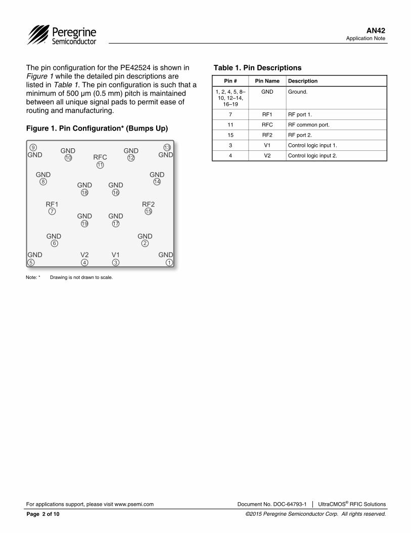
The pin configuration for the PE42524 is shown in Figure 1 while the detailed pin descriptions are listed in Table 1. The pin configuration is such that a minimum of 500 µm (0.5 mm) pitch is maintained between all unique signal pads to permit ease of routing and manufacturing.
Figure 1. Pin Configuration* (Bumps Up)
Table 1. Pin Descriptions
Pin # Pin Name Description
1, 2, 4, 5, 8–10, 12–14,
16–19
GND Ground.
7 RF1 RF port 1.
11 RFC RF common port.
15 RF2 RF port 2.
3 V1 Control logic input 1.
4 V2 Control logic input 2.
Note: * Drawing is not drawn to scale.
1345
9 13
15
14
1618
1719
1210
8
7
6
11
2
GNDV1V2GND
GND GND
GND
GND GND
GNDGND GND
GND
RF1 RF2
GND
GNDRFC GND

Application Note AN42
Page 3 of 10
Document No. DOC-64793-1 www.psemi.com
©2015 Peregrine Semiconductor Corp. All rights reserved.
For applications support, please visit www.psemi.com
Landing Patterns
The PE42524 is configured with a 0.5 mm, or 500 µm, minimum ball pitch. Thin film technologies can readily meet the line width and spacing critical dimensions (CD) of 100 µm or less, but other thick film and PCB processes generally require far less stringent CDs to reach reasonable and consistent manufacturing yields. The comparatively wide 500 µm ball pitch is intended to support the larger CD requirements and enable assembly of the die directly to RF PCB boards. To obtain the best microwave performance, specific metallization and via patterns have been defined and implemented to provide measured results for the PE42524. These recommended layouts can be downloaded from the Peregrine Semiconductor website.
Alumina Substrate
Figure 2 depicts two recommended metallization patterns and via placements for alumina substrate carriers on which the PE42524 is assembled. The first substrate carrier shown in Figure 2a uses an alumina thickness of 10 mil with 8 mil diameter vi-as. The 50Ω coplanar waveguide with ground (CPWG) transmission line width and spacing di-mensions are 5.13 and 3.54 mil, respectively. Addi-tionally, an important CPWG line dimension at the RF common port (RFC) uses a line length and width of 17.5 and 2.8 mil, respectively. This sub-strate carrier is referenced as PRT58123 and is used for the sampling and the characterization of the PE42524 SPDT. A second substrate carrier al-so uses 10 mil alumina but has an increased num-ber of filled vias. The PRT60965, shown in Figure 2b, has 28 vias compared to 18 vias in the PRT58123 version. In general, should the end application need to use a different thickness alumina between 5–10 mil, the critical dimensions of line width and spacing and via diameter can be readily scaled to accommodate the specific thickness requirements.
Figure 2a. PRT58123 10 mil Alumina Substrate Metallization and Via Pattern Used for Characterization and Sample Units
Figure 2b. PRT60965 10 mil Alumina Substrate Metallization and Via Pattern Recommended for Maximum Isolation
Substrate OutlineMetalization PatternVia Locations
Solder MaskBall Center PointPE42524 Die Outline
Substrate OutlineMetalization PatternVia Locations
Solder MaskBall Center PointPE42524 Die Outline

Application Note AN42
Page 4 of 10 ©2015 Peregrine Semiconductor Corp. All rights reserved.
Document No. DOC-64793-1 UltraCMOS® RFIC Solutions For applications support, please visit www.psemi.com
As mentioned earlier, RF performance can be af-fected by the specifics of the metallization and via patterns. This is shown in Figure 3, which depicts the changes in isolation levels due to differences in the number of vias and minor changes in the metal pattern. The best isolation is achieved using the PRT60965 design. In comparison, the substrate used for sampling and characterizing the PE42524, PRT58123, is also shown.
Figure 3. Isolation Performance Comparison Between 10 mil Alumina Substrate Carriers PRT58123 and PRT60965 Metallization and Via Patterns*
Note: * The PRT60965 is the recommended pattern for maximum isolation. Isolation for the 8 mil Rogers 4003 (PRT44405) substrate carrier is also shown.
The isolation of the PRT58123 substrate carrier at 40 GHz degrades to 35 dB while the PRT60965 ver-sion has greater than 40 dB across the entire range. Isolation performance for the Rogers 4003 PCB sub-strate (PRT44405) is also shown in Figure 3. The PCB vias are located on entirely different coordi-nates, since the substrate material gives different trace patterns compared to the alumina versions.
-80
-70
-60
-50
-40
-30
0 5 10 15 20 25 30 35 40
Isol
atio
n (d
B)
Freq (GHz)
10mil PRT58123Isolation (dB)
10mil PRT60965Isolation (dB)
8mil Rogers 4003Isolation (dB)

Application Note AN42
Page 5 of 10
Document No. DOC-64793-1 www.psemi.com
©2015 Peregrine Semiconductor Corp. All rights reserved.
For applications support, please visit www.psemi.com
Figure 4. Assembled PE42524 on Alumina Substrate PRT58123
To minimize unwanted wicking of individual solder balls from the local connection point, some form of solder stop is strongly recommended. This could be a marking or protective polymer layer, or some oth-er material that the substrate manufacturer may rec-ommend. The thickness of the solder stop is sug-gested to be in the 15–25 µm range to assure its effectiveness in stopping solder wicking while not touching the face of the PE42524 die. Finally, the line width and spacing at the edge of the RF lines in the landing pattern is configured for 150 µm pitch Ground-Signal-Ground (G-S-G) RF probes to facilitate accurate measurements. The user should feel free to modify and integrate the landing pattern anywhere outside the die outline to align with the higher level assembly and substrate design requirements.
RFC
Alumina substrate boardThickness: 0.01 in.
εR = 9.9
RF1
V1 V2
RF2PE42524
DIE

Application Note AN42
Page 6 of 10 ©2015 Peregrine Semiconductor Corp. All rights reserved.
Document No. DOC-64793-1 UltraCMOS® RFIC Solutions For applications support, please visit www.psemi.com
Rogers 4003 Printed Circuit Board
A metallization and via pattern PRT44405 has also been generated for a Rogers 4003 substrate. Fig-ure 5 shows the pattern that is designed for an 8 mil board thickness. This board layout is config-ured to work with high frequency SMA connectors, but the basic pattern can be used to create an RF-probable PCB. Such a PCB is shown in Figure 6. The measured performance of the PE42524, when assembled to the PCB and properly de-embedded, results in performance that is comparable to that achieved using the alumina-based design.
Important dimensions, in addition to the 50Ω trans-mission line width and spacing, include the dimen-sions of the thinner lines right at the PE42524 SPDT RF ports. The RF common port (RFC) uses a line length and width of 18 and 6 mil, respectively, and the two RF ports RF1 and RF2 use line length and width of 13 and 6 mil, respectively. Via diame-ters are 8 mil except in the region under the die, which uses 5 mil diameter.
Figure 5. PCB Rogers 4003 PRT44405 Metallization and Via Patterns
Figure 6. PCB Rogers 4003 Evaluation Board Based Upon the PRT44405 Metallization and Via Patterns
Substrate OutlineMetalization PatternVia Locations
Solder MaskBall Center PointPE42524 Die Outline
Application Note AN42
Page 7 of 10
Document No. DOC-64793-1 www.psemi.com
©2015 Peregrine Semiconductor Corp. All rights reserved.
For applications support, please visit www.psemi.com
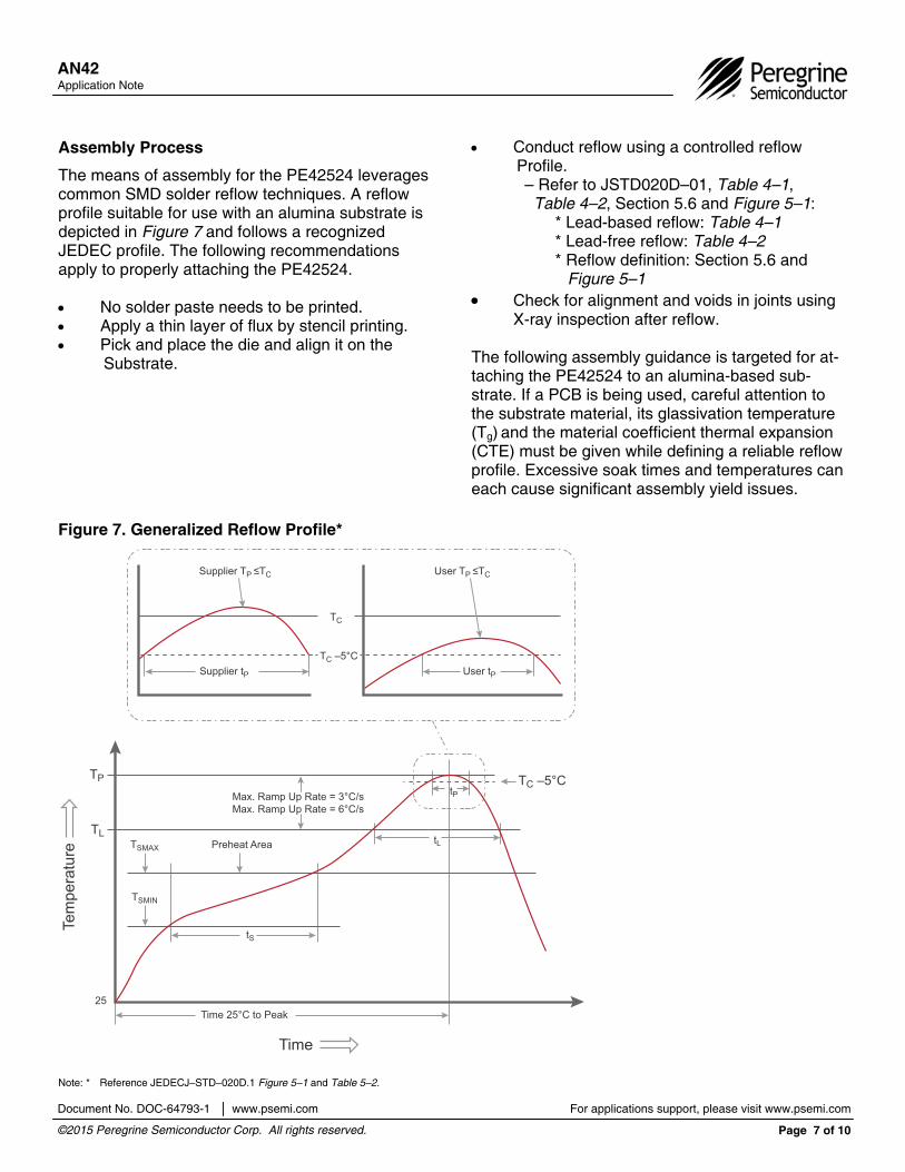
Assembly Process
The means of assembly for the PE42524 leverages common SMD solder reflow techniques. A reflow profile suitable for use with an alumina substrate is depicted in Figure 7 and follows a recognized JEDEC profile. The following recommendations apply to properly attaching the PE42524. No solder paste needs to be printed. Apply a thin layer of flux by stencil printing. Pick and place the die and align it on the Substrate.
Figure 7. Generalized Reflow Profile*
Note: * Reference JEDECJ–STD–020D.1 Figure 5–1 and Table 5–2.
Conduct reflow using a controlled reflow Profile. – Refer to JSTD020D–01, Table 4–1, Table 4–2, Section 5.6 and Figure 5–1: * Lead-based reflow: Table 4–1 * Lead-free reflow: Table 4–2 * Reflow definition: Section 5.6 and Figure 5–1 Check for alignment and voids in joints using
X-ray inspection after reflow. The following assembly guidance is targeted for at-taching the PE42524 to an alumina-based sub-strate. If a PCB is being used, careful attention to the substrate material, its glassivation temperature (Tg) and the material coefficient thermal expansion (CTE) must be given while defining a reliable reflow profile. Excessive soak times and temperatures can each cause significant assembly yield issues.
TC
Supplier tP User tP
User TP ≤TCSupplier TP ≤TC
TC –5°C
TC –5°C TP
TL
Time 25°C to Peak
Tem
pera
ture
Time
25
tLTSMAX Preheat Area
Max. Ramp Up Rate = 3°C/sMax. Ramp Up Rate = 6°C/s
TSMIN
tS
tP

Application Note AN42
Page 8 of 10 ©2015 Peregrine Semiconductor Corp. All rights reserved.
Document No. DOC-64793-1 UltraCMOS® RFIC Solutions For applications support, please visit www.psemi.com
Measured Performance
Figure 8 shows the insertion loss behavior to 40 GHz of the PE42524 when mounted to the PRT58123 alumina substrate carrier and measured in an RF probe configuration. Figure 9 shows the >45 dB of isolation at 30 GHz and the RFC and RF1 active port return losses.
Figure 8. Insertion Loss of PE42524 on 10 mil Alumina Substrate Carrier
Figure 9. Isolation and Return Loss of PE42524 on 10 mil Alumina Substrate Carrier
-6
-5
-4
-3
-2
-1
0
0 5 10 15 20 25 30 35 40
Inse
rtio
n Lo
ss (d
B)
Freq (GHz)
Insertion Loss (dB)
-80
-70
-60
-50
-40
-30
-20
-10
0
0 5 10 15 20 25 30 35 40
Isol
atio
n &
Ret
urn
Loss
(dB
)
Freq (GHz)
RFC (dB) RF1 (dB) Isolation (dB)
Application Note AN42
Page 9 of 10
Document No. DOC-64793-1 www.psemi.com
©2015 Peregrine Semiconductor Corp. All rights reserved.
For applications support, please visit www.psemi.com
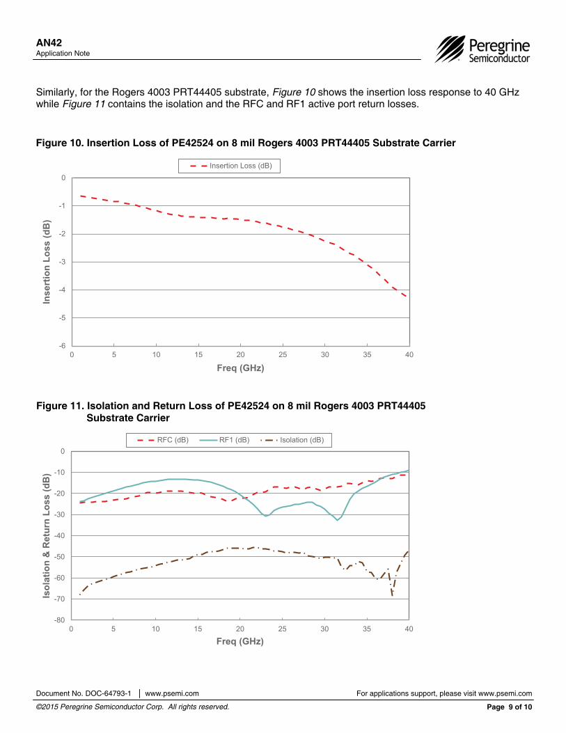
Figure 10. Insertion Loss of PE42524 on 8 mil Rogers 4003 PRT44405 Substrate Carrier
Similarly, for the Rogers 4003 PRT44405 substrate, Figure 10 shows the insertion loss response to 40 GHz while Figure 11 contains the isolation and the RFC and RF1 active port return losses.
Figure 11. Isolation and Return Loss of PE42524 on 8 mil Rogers 4003 PRT44405 Substrate Carrier
-6
-5
-4
-3
-2
-1
0
0 5 10 15 20 25 30 35 40
Inse
rtio
n Lo
ss (d
B)
Freq (GHz)
Insertion Loss (dB)
-80
-70
-60
-50
-40
-30
-20
-10
0
0 5 10 15 20 25 30 35 40
Isol
atio
n &
Ret
urn
Loss
(dB
)
Freq (GHz)
RFC (dB) RF1 (dB) Isolation (dB)
Application Note AN42
Page 10 of 10 ©2015 Peregrine Semiconductor Corp. All rights reserved.
Document No. DOC-64793-1 UltraCMOS® RFIC Solutions For applications support, please visit www.psemi.com
The information in this document is believed to be reliable. However, Peregrine assumes no liability for the use of this information. Use shall be entirely at the user’s own risk. No patent rights or licenses to any circuits described in this datasheet are implied or granted to any third party. Peregrine’s products are not designed or intended for use in devices or systems intended for surgical implant, or in other applications intended to support or sustain life, or in any application in which the failure of the Peregrine product could create a situation in which personal injury or death might occur. Peregrine assumes no liability for damages, including consequential or incidental damages, arising out of the use of its products in such applications. The Peregrine name, logo, UltraCMOS and UTSi are registered trademarks and HaRP, MultiSwitch and DuNE are trademarks of Peregrine Semiconductor Corp. All other trademarks mentioned herein are the property of their respective owners. Peregrine products are protected under one or more of the following U.S. Patents: http://patents.psemi.com.
Conclusion
The PE42524 is the first microwave switch to be offered by Peregrine Semiconductor. The PE42524 brings competitive insertion loss, exceptional isolation and the usual high linearity and power handling Peregrine is known for to a market that can benefit from the uniformity and availability that UltraCMOS affords to every market it enters. To achieve high performance at these frequencies, extreme care must be taken to eliminate any stray parasitics affecting the RF channel. This application note provides guidance necessary for achieving the optimum performance from the PE42524. Landing patterns in different substrate technologies have been described, all of which have shown comparable performance up to 40 GHz. Complete CAD files of the physical layouts are available from Pere-grine’s website to help facilitate the integration of the PE42524 into higher-level assemblies and systems.