application note rev1 - rs components
TRANSCRIPT
Application Note rev1.8
Samsung Electronics
LM231A (2323L)
Index
2
1. Introduction Page
1.1 Product Description
1.1.1 Compact & reliable light source (LM231A) 4
1.2 Product Information
1.2.1 Feature and dimension 5
1.2.2 Product code and binning 6
1.2.3 Beam angle vs. color shift (delta u’v’) 9
1.2.4 Polar Intensity diagram 9
2. Package Characteristics
2.1 Thermal Characteristics
2.1.1 Test DUT & thermal measurement point – Ts 10
2.1.2 Thermal resistance 11
2.2 Electrical Characteristics 12
2.3 Optical Characteristics
2.3.1 Luminous flux & efficacy ratio vs. current & Ts 13
2.3.2 Color shift vs. current & Ts 14
2.4 Mechanical Characteristics
2.4.1 Derating curve 15
3
2.5 Thermal simulations
2.5.1 Reference PCB modeling 18
2.5.2 PCB material effects 18
2.5.3 Via hole effects 19
2.5.4 Copper pad thickness effects 19
2.6 S.M.T Guide
2.6.1 Recommended land pattern & solder paste 20
2.6.2 Pick & Place 21
2.6.3 Reflow profile and conditions 22
2.7 Mechanical Consideration
2.7.1 Handling guide 23
3. Application
3.1 Kitting bin solution
3.1.1 Array solution for color uniformity 24
3.1.2 Implementation of kitting bin application 25
4. Revision History 27
4
1.1 Product Description
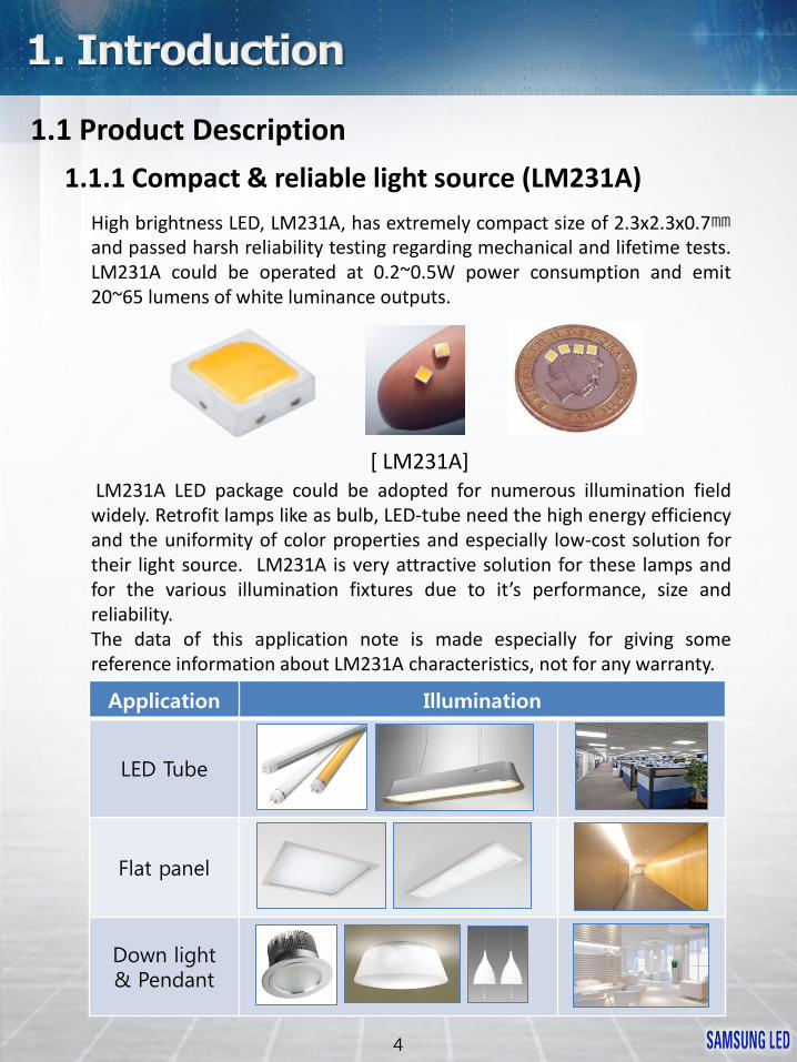
1.1.1 Compact & reliable light source (LM231A)
High brightness LED, LM231A, has extremely compact size of 2.3x2.3x0.7㎜ and passed harsh reliability testing regarding mechanical and lifetime tests. LM231A could be operated at 0.2~0.5W power consumption and emit 20~65 lumens of white luminance outputs.
[ LM231A] LM231A LED package could be adopted for numerous illumination field widely. Retrofit lamps like as bulb, LED-tube need the high energy efficiency and the uniformity of color properties and especially low-cost solution for their light source. LM231A is very attractive solution for these lamps and for the various illumination fixtures due to it’s performance, size and reliability. The data of this application note is made especially for giving some reference information about LM231A characteristics, not for any warranty.
Application Illumination
LED Tube
Flat panel
Down light & Pendant

5
1.2 Product Information
1.2.1 Feature and dimension
LM231A has a compact dimension. - SMD Type LED Package : 2.3 x 2.3 x 0.7t mm - Electrically cathode pad plays a key role as a main thermal pad
[ LM231A Package Dimension ]
LM231A is a very attractive solution for reliability. - GaN / Al2O3 Chip & SMD type package - Robust of silicone mold material - Eco-friendly : RoHS compliant - Maximum compressing force is 15N on the silicone mold
Anode (+)
Cathode (-)
LED
Zener
Diode
Top View Bottom View Side View
Lead Frame
(Anode)
Mold (Silicone)
Lead Frame
(Cathode)
Cathode Mark
Phosphor & Resin
Unit : ㎜ Tolerance : ±0.1
6
1.2 Product Information
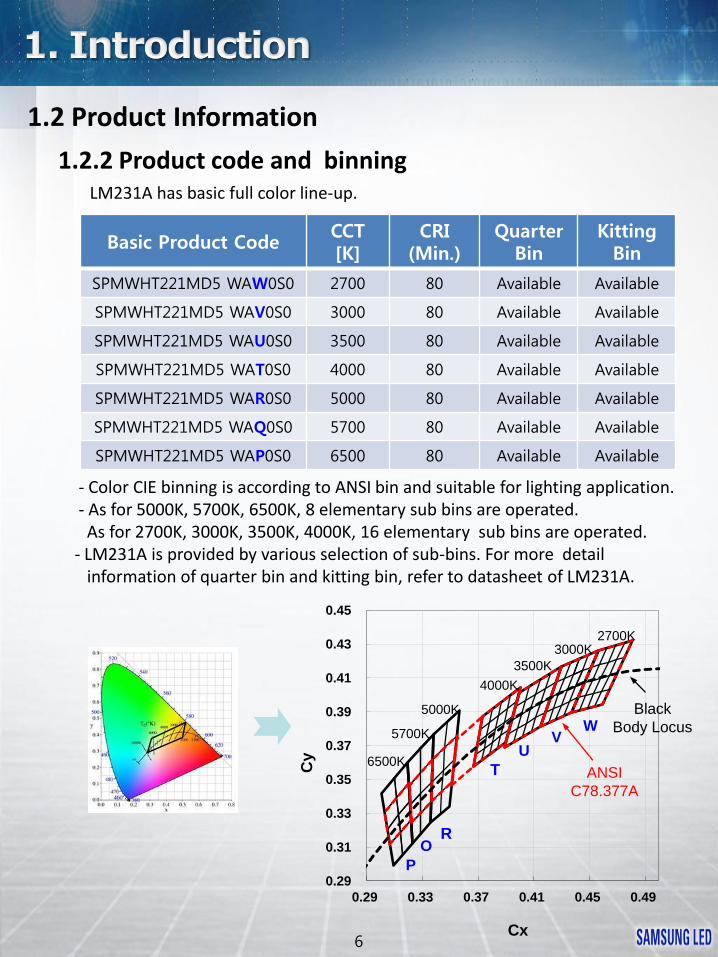
1.2.2 Product code and binning LM231A has basic full color line-up.
Basic Product Code CCT [K]
CRI (Min.)
Quarter Bin
Kitting Bin
SPMWHT221MD5 WAW0S0 2700 80 Available Available
SPMWHT221MD5 WAV0S0 3000 80 Available Available
SPMWHT221MD5 WAU0S0 3500 80 Available Available
SPMWHT221MD5 WAT0S0 4000 80 Available Available
SPMWHT221MD5 WAR0S0 5000 80 Available Available
SPMWHT221MD5 WAQ0S0 5700 80 Available Available
SPMWHT221MD5 WAP0S0 6500 80 Available Available
- Color CIE binning is according to ANSI bin and suitable for lighting application. - As for 5000K, 5700K, 6500K, 8 elementary sub bins are operated. As for 2700K, 3000K, 3500K, 4000K, 16 elementary sub bins are operated. - LM231A is provided by various selection of sub-bins. For more detail information of quarter bin and kitting bin, refer to datasheet of LM231A.
0.29
0.31
0.33
0.35
0.37
0.39
0.41
0.43
0.45
0.29 0.33 0.37 0.41 0.45 0.49
Cy
Cx
R
T
P
U V
Q
W
6500K
5700K
5000K
4000K
3500K
3000K 2700K
ANSI
C78.377A
Black
Body Locus
7
@If=65mA Ts=25℃
Lum
ino
us
Flu
x [l
m]
LM231A has 3 kinds of fundamental binning, - Voltage, Flux, Color - Luminous flux (Iv (Φv)) is divided by 3 rank – S1, S2, S3 - sorting current and ambient temperature is 65mA and 25℃ respectively.
Lum
ino
us
Effi
cacy
[lm
/W]
@If=65mA Ts=25℃
With the same typical forward voltage,2.95V, luminous efficacy (lm/W) at each flux rank are shown in below graph. From datasheet, highest and lowest luminous efficacy could be expected by considering highest luminous rank with lowest forward voltage rank and vice versa.
18
20
22
24
26
28
30
32
W0-2
700K
(80Ra)
V0-3
000K
(80Ra)
U0-3
500K
(80Ra)
T0-4
000K
(80Ra)
R0-5
000K
(80Ra)
Q0-5
700K
(80Ra)
P0-6
500K
(80Ra)
Luminous Flux Rank - S1. S2,S3
S3
S2
S1
80
90
100
110
120
130
140
150
160
170
180
W0-2
700K
(80Ra)
V0-3
000K
(80Ra)
U0-3
500K
(80Ra)
T0-4
000K
(80Ra)
R0-5
000K
(80Ra)
Q0-5
700K
(80Ra)
P0-6
500K
(80Ra)
Luminous Efficacy @65mA
Max.
S3
S2
S1
Min.

8
- Forward voltage(VF) is divided to 5 rank - A1,A2,A3,A4,A5
AZ A1 A2 A3 A4
2.6 2.7 2.8 2.9 3 3.1 3.2 3.3
Forward Voltage [V]
Lum
ino
us
Effi
cacy
[lm
/W]
@If=100mA Ts=25℃
Lum
ino
us
Effi
cacy
[lm
/W] @If=150mA
Ts=25℃
80
90
100
110
120
130
140
150
160
170
180
W0-2
700K
(80Ra)
V0-3
000K
(80Ra)
U0-3
500K
(80Ra)
T0-4
000K
(80Ra)
R0-5
000K
(80Ra)
Q0-5
700K
(80Ra)
P0-6
500K
(80Ra)
Luminous Efficacy @100mA
Max.
S3
S2
S1
Min.
80
90
100
110
120
130
140
150
160
170
180
W0-2
700K
(80Ra)
V0-3
000K
(80Ra)
U0-3
500K
(80Ra)
T0-4
000K
(80Ra)
R0-5
000K
(80Ra)
Q0-5
700K
(80Ra)
P0-6
500K
(80Ra)
Luminous Efficacy @150mA
Max.
S3
S2
S1
Min.

9
1.2 Product Information
1.2.3 Beam angle vs. color shift (delta u’v’)
1.2.4 Polar intensity diagram
Optical spectra of LM231A are shown like as below graph at each CCT 3000K and 5000K. Measured data is just for representative reference only.
Viewing angle describes the spatial distribution and the value is 120°(FWHM, Full width at half maximum), FWHM is the difference between the angles corresponding to 50% of the maximum intensity.
0.00
0.01
0.02
0.03
0.04
0.05
-90 -75 -60 -45 -30 -15 0 15 30 45 60 75 90
Delta u
'v'
Angle (degree)
3000K
5000K
-90
+90
10
2.1 Thermal Characteristics
The typical value of LM231A is well presented on datasheet. But in case of the real design domain, typical value might be changeable as to operating conditions(current, voltage), product structure (Effects on thermal dissipation) and environment conditions. And performance objectives in product newly developed should be considered in various point of important factors. Most of all design factor, the thermal factor is the main key of expecting the target of LED performance. Basically the main LED properties of luminous flux(lm), forward voltage(VF) and color (Cx, Cy chromaticity) is depending on the thermal condition. In this note, we show that how the characteristics of LED is changed with variation of temperature. First, the reference temperature should be clearly defined as solder temperature of cathode pad, which is expressed as ‘Ts’ and is measurement point for a reference temperature. LED chip is usually mounted on cathode side where the most of heat can release. For measuring ‘Ts’, the thermo couple cable have to be connected with the cathode pad as shown in above figure.
Ts point
2.1.1 Test DUT & thermal measurement point - Ts
Copper electro-thermal pad (Cathode)
- condition : 50mA, 25℃ - Cu pad of Cathode : 44,400 W/㎡ (99.5%) - Cu pad of Anode : 210 W/㎡ (0.5%) Cathode
Anode
Cathode mark
Recommended measuring site
[ DUT (Device under Test) & Ts point ]
High heat density (W/ ㎡)
Low heat density (W/ ㎡)
[ Heat dissipation simulation ]

11
2.1 Thermal Characteristics
It is not easy to measure LED chip temperature, TJ, directly. But most of lighting designer need LED chip temperature information to confirm their final product reliability. For these reason, designer use thermal resistance of LED package, RTH , to estimate chip temperature. Solder temperature, TS, of Led package could be easily measured and then add delta temperature between solder and chip, RTH (J-S) x PLED , on TS. See equation (1), (2). Finally designer could recognize how degree LED junction temperature can rise-up from these steps.
2.1.2 Thermal resistance
Aluminium Plate
PCB Dielectric layerPCB Solder Pads
Classical TIM to heat-sink
Heat Sink
Solder to PCB
Molding
Chip attach material to substrate
LED Chip Phosphor
Bonding wire
TJ : Junction Temp.
TS : Solder Temp.
TB : Board Temp.
RJ-LFTLF : Lead Frame substrate
Lead-Frame (substrate)
TC : Case Temp.
TA : Ambient Temp.
RJS : Junction-SolderRLF-S
RSB : Solder to Board
RBC : Board to Case
RCA : Case to Air
PLED : Thermal Source
Tambient : Thermal Ground
RTH is measured according to JEDEC Standards, JESD51-1, 51-14. We use T3Ster to evaluate thermal resistance.
Average value of RTH (J-S) : 18.8 - Number of samples : 11ea - sigma value : 1.5
[ Thermal system - vertical diagram ]
RT T
PowerTH
J S
LED
T T R PowerJ S TH LED *------ (1) ------ (2)
1.00E-05
1.00E-04
1.00E-03
1.00E-02
1.00E-01
1.00E+00
1.00E+01
1.00E+02
1.00E+03
0 5 10 15 20 25 30 35 40
k(W
2s/
K2)
Rth(K/W)
Chip
2~3℃/W
Die Bonding
Epoxy
13℃/W
RTH(J-S) L/F
18~19℃/W McPCB
25℃/W

12
2.2 Electrical Characteristics If constant current is driven into LED package, forward voltage of the LED would be dropped as temperature goes up, therefore IV curve would shift to the left side. In right side graph, IV curve of LM231A is shown at various TS temperature. Let us consider about power consumption. From IV curve, power consumption could be represented by forward current or forward voltage. Below two graphs show these relations. And these graphs show very meaningful point of LED operation.
As shown in below figure, If driving mode is set by constant current(C-C) mode, the variation of power consumption becomes more less than constant voltage (C-V) mode over Ts temperature. In order to get stable lighting output, LED should be driven by constant current driving method.
[Power consumption with constant current mode]
[Power consumption with constant voltage mode]
[Forward Current vs. Forward Voltage]
40
60
80
100
120
140
160
2.7 2.8 2.9 3.0 3.1 3.2 3.3 F
orw
ard
Cu
rre
nt (m
A)
Forward Voltage (V)
25℃
50℃
75℃
90℃
40
60
80
100
120
140
160
0.0 0.1 0.2 0.3 0.4 0.5 0.6
Forw
ard
Cu
rre
nt (m
A)
Power Consumption (W)
Forward Current vs. Power Consumption
25℃
50℃
75℃
90℃
2.7
2.8
2.9
3.0
3.1
3.2
3.3
0.0 0.1 0.2 0.3 0.4 0.5 0.6
Forw
ard
Vo
lta
ge
(V
)
Power Consumption (W)
Forward Voltage vs. Power Consumption
25℃
50℃
75℃
90℃
13
2.3 Optical Characteristics
2.3.1 Luminous flux & efficacy ratio vs. current & Ts
At datasheet, luminous flux of each rank is presented in detail. In left graph, relative luminous flux ratio is presented depending on each TS temperature. Each color CCT has similar flux ratio between 2700K and 5000K. The reference point of flux ratio is set at the operation current of 65mA. Therefore we can estimate 185% luminous flux ratio at 140mA and Ts of 75 ℃ respectively.
Voltage binning is also presented at datasheet. If under the same typical voltage of 2.95V, relative luminous efficacy ratio could be presented like as right side graph. At Ts of 75℃, and driving current of 100mA, efficacy ratio of 89% could be roughly expected.
[Relative Luminous Flux Ratio vs. Forward Current]
[Relative Efficacy Ratio vs. Forward Current]
40%
50%
60%
70%
80%
90%
100%
110%
120%
130%
140%
150%
160%
170%
180%
190%
200%
210%
220%
40 50 60 70 80 90 100 110 120 130 140 150
Re
lative
Lu
min
ou
s F
lux R
atio (
%)
Forward Current (mA)
25℃
50℃
75℃
90℃
70%
75%
80%
85%
90%
95%
100%
105%
110%
40 50 60 70 80 90 100 110 120 130 140 150
Re
lative
Eff
ica
cy R
atio (
%)
Forward Current (mA)
25℃
50℃
75℃
90℃
0.32
0.33
0.34
0.35
0.36
0.37
0.38
0.39
0.33 0.34 0.35 0.36
Cy
Cx
ANSI
C78.377A
Black
Body Locus
R1
R2
R7
R8 R3
R4 R5
R6 R9
RA
0.339
0.341
0.343
0.345
0.347
0.349
0.351
0.353
0.355
0.357
0.359
0.334 0.336 0.338 0.340 0.342 0.344
Cy
Cx
65mA
100mA
150mA
0.38
0.39
0.40
0.41
0.42
0.43
0.44
0.43 0.44 0.45 0.46 0.47 0.48 0.49
Cy
Cx
Black
Body Locus
ANSI
C78.377A
W1 W4
WG WD
0.407
0.409
0.411
0.413
0.415
0.458 0.460 0.462 0.464 0.466
Cy
Cx
65mA
100mA
150mA
14
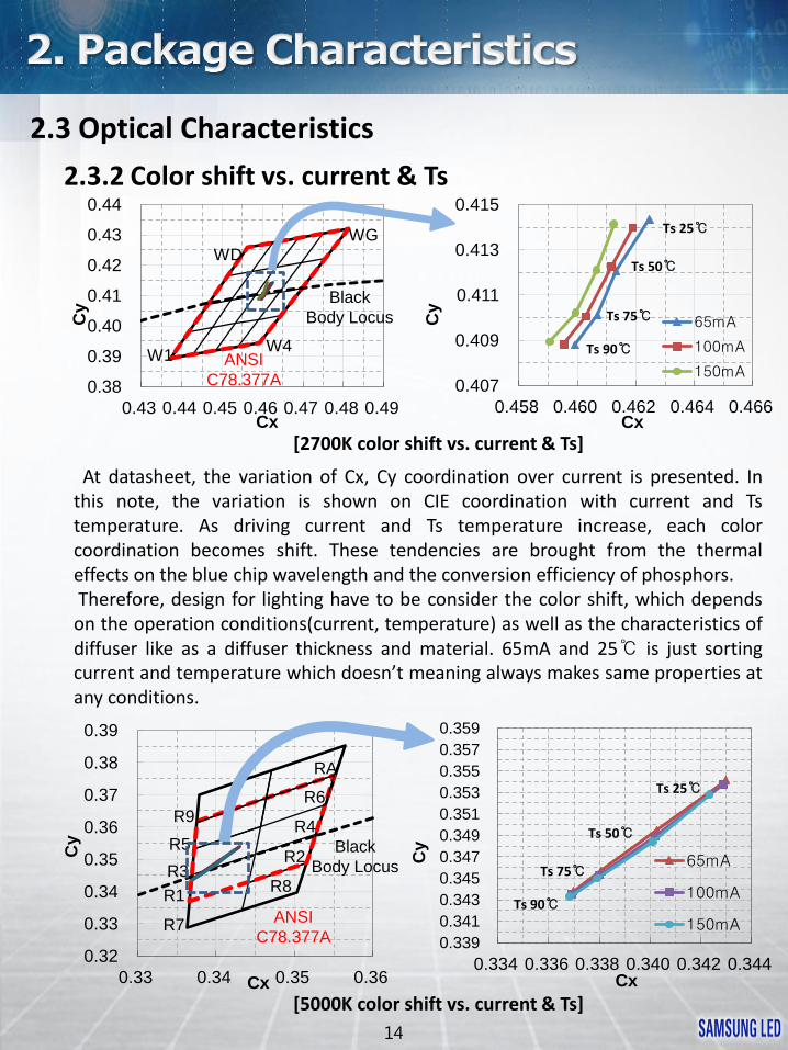
2.3 Optical Characteristics
2.3.2 Color shift vs. current & Ts
At datasheet, the variation of Cx, Cy coordination over current is presented. In this note, the variation is shown on CIE coordination with current and Ts temperature. As driving current and Ts temperature increase, each color coordination becomes shift. These tendencies are brought from the thermal effects on the blue chip wavelength and the conversion efficiency of phosphors. Therefore, design for lighting have to be consider the color shift, which depends on the operation conditions(current, temperature) as well as the characteristics of diffuser like as a diffuser thickness and material. 65mA and 25℃ is just sorting current and temperature which doesn’t meaning always makes same properties at any conditions.
Ts 90℃
[2700K color shift vs. current & Ts]
[5000K color shift vs. current & Ts]
Ts 25℃
Ts 50℃
Ts 75℃
Ts 90℃
Ts 25℃
Ts 50℃
Ts 75℃
0
25
50
75
100
125
150
175
200
0 10 20 30 40 50 60 70 80 90
Forw
ard
curr
ent
[mA
]
Ambient Temperature [℃]
Derating Curve
Rth(j-a) 50″/W
Rth(j-a) 100″/W
Rth(j-a) 150″/W
Rth(j-a) 200″/W
Rth(j-a) 300″/W
15
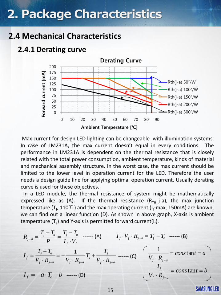
2.4 Mechanical Characteristics
2.4.1 Derating curve
Max current for design LED lighting can be changeable with illumination systems. In case of LM231A, the max current doesn’t equal in every conditions. The performance in LM231A is dependent on the thermal resistance that is closely related with the total power consumption, ambient temperature, kinds of material and mechanical assembly structure. In the worst case, the max current should be limited to the lower level in operation current for the LED. Therefore the user needs a design guide line for applying optimal operation current. Usually derating curve is used for these objectives. In a LED module, the thermal resistance of system might be mathematically expressed like as (A). If the thermal resistance (RTH j-a), the max junction temperature (TJ, 110℃) and the max operating current (If-max, 150mA) are known, we can find out a linear function (D). As shown in above graph, X-axis is ambient temperature (Ta) and Y-axis is permitted forward current(If).
RT T
P
T T
I Vj a
j a j a
f f
I V R T Tf f j a f a
IT T
V R V RT
T
V Rf
j a
f j a f j a
a
j
f j a
1 1
V Rcons t a
f j a
tan
T
V Rcons t b
j
f j a
tanI a T bf a
------ (A) ------ (B)
------ (C)
------ (D)
16
Case IF[mA]/LED P[W]/LED TJ[℃] Ts[℃] Ta[℃] RJ-a [℃/W]
① 30 0.08 49 47.4 25 300 ② 65 0.19 82 78.2 25 300 ③ 100 0.3 115 109 25 300
0 25 50 75
100 125 150 175 200
0 10 20 30 40 50 60 70 80 90 Forw
ard
curr
ent
[mA
] Ambient Temperature [℃]
Rth(j-a) 50″/W
Rth(j-a) 100″/W
Rth(j-a) 150″/W
Rth(j-a) 200″/W
Rth(j-a) 300″/W
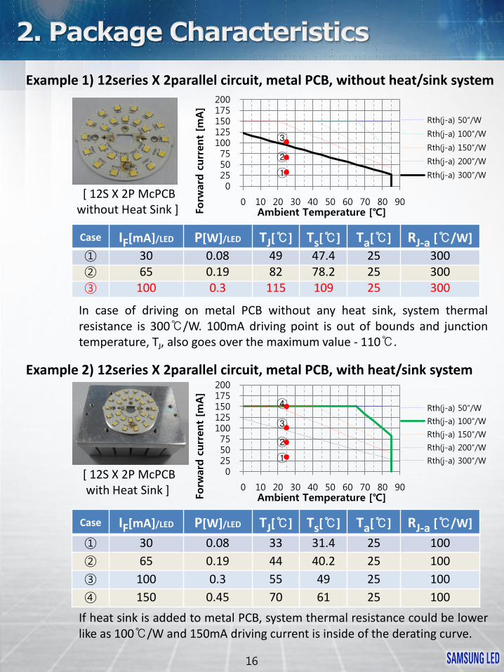
[ 12S X 2P McPCB without Heat Sink ]
Example 1) 12series X 2parallel circuit, metal PCB, without heat/sink system
Example 2) 12series X 2parallel circuit, metal PCB, with heat/sink system
Case IF[mA]/LED P[W]/LED TJ[℃] Ts[℃] Ta[℃] RJ-a [℃/W]
① 30 0.08 33 31.4 25 100
② 65 0.19 44 40.2 25 100
③ 100 0.3 55 49 25 100
④ 150 0.45 70 61 25 100
[ 12S X 2P McPCB with Heat Sink ]
0 25 50 75
100 125 150 175 200
0 10 20 30 40 50 60 70 80 90
Forw
ard
curr
ent
[mA
]
Ambient Temperature [℃]
Rth(j-a) 50″/W
Rth(j-a) 100″/W
Rth(j-a) 150″/W
Rth(j-a) 200″/W
Rth(j-a) 300″/W
①
②
③
①
②
③
④
In case of driving on metal PCB without any heat sink, system thermal resistance is 300℃/W. 100mA driving point is out of bounds and junction temperature, TJ, also goes over the maximum value - 110℃.
If heat sink is added to metal PCB, system thermal resistance could be lower like as 100℃/W and 150mA driving current is inside of the derating curve.
17
0 25 50 75
100 125 150 175 200
0 10 20 30 40 50 60 70 80 90 Forw
ard
curr
ent
[mA
] Ambient Temperature [℃]
Rth(j-a) 50″/W
Rth(j-a) 100″/W
Rth(j-a) 150″/W
Rth(j-a) 200″/W
Rth(j-a) 300″/W
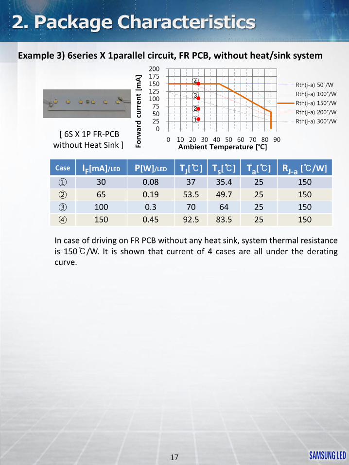
[ 6S X 1P FR-PCB without Heat Sink ]
Example 3) 6series X 1parallel circuit, FR PCB, without heat/sink system
①
②
③
In case of driving on FR PCB without any heat sink, system thermal resistance is 150℃/W. It is shown that current of 4 cases are all under the derating curve.
Case IF[mA]/LED P[W]/LED TJ[℃] Ts[℃] Ta[℃] RJ-a [℃/W]
① 30 0.08 37 35.4 25 150
② 65 0.19 53.5 49.7 25 150
③ 100 0.3 70 64 25 150
④ 150 0.45 92.5 83.5 25 150
④

Material CEM-1 FR-4 McPCB
Cu 1.0 ounce 2-layer PCB 1.0t
No via hole 65mA driving
RTH 22.0℃/W 17.8℃/W 6.3℃/W
TC 69.3℃ 65.0℃ 47.8℃
Cu clad
Prepreg
LED
Copper
Copper
Aluminum Heat Sink
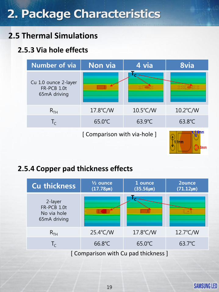
2.5 Thermal Simulations
2.5.1 Reference PCB modeling
18
Through the thermal simulation of LM231A, we can consider how the PCB structure shall influence on TC (PCB case temperature). If TC is high, then we can expect high TJ and the rapid degradation of luminous flux. And modeling DUT is bar-type PCB which is assembled on aluminum heat sink. In this note, we simulated thermal behaviors with 3kinds of PCBs. The key variables are the kinds of PCB material, the existence of via hole and copper pad thickness in PCB. First of all, the effects of PCB material is the dominant factor for TC in high power applications, which can generate large heat. for example. For example, For LED bulb(which can replace 60W incandescent lamp), it should be recommended for using metal-core PCB board for normal operation condition.
[Reference PCB shape] Top view Side view
2.5.2 PCB material effects
[ Comparison with PCB materials ]
TC
TC
19
2.5 Thermal Simulations
2.5.3 Via hole effects
Cu thickness ½ ounce (17.78㎛)
1 ounce (35.56㎛)
2ounce (71.12㎛)
2-layer FR-PCB 1.0t No via hole
65mA driving
RTH 25.4℃/W 17.8℃/W 12.7℃/W
TC 66.8℃ 65.0℃ 63.7℃
2.5.4 Copper pad thickness effects
[ Comparison with Cu pad thickness ]
Number of via Non via 4 via 8via
Cu 1.0 ounce 2-layer FR-PCB 1.0t
65mA driving
RTH 17.8℃/W 10.5℃/W 10.2℃/W
TC 65.0℃ 63.9℃ 63.8℃
[ Comparison with via-hole ]
TC
TC
( O ) ( X )
20
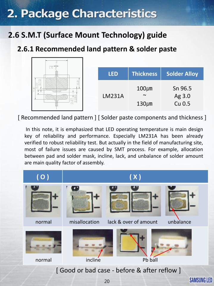
[ Recommended land pattern ]
2.6 S.M.T (Surface Mount Technology) guide
2.6.1 Recommended land pattern & solder paste
LED Thickness Solder Alloy
LM231A 100㎛
~ 130㎛
Sn 96.5 Ag 3.0 Cu 0.5
[ Solder paste components and thickness ]
In this note, it is emphasized that LED operating temperature is main design key of reliability and performance. Especially LM231A has been already verified to robust reliability test. But actually in the field of manufacturing site, most of failure issues are caused by SMT process. For example, allocation between pad and solder mask, incline, lack, and unbalance of solder amount are main quality factor of assembly.
[ Good or bad case - before & after reflow ]
normal misallocation lack & over of amount unbalance
normal incline Pb ball

- SMT Equipment process and its conditions
21
- Pick up tool (Collet)
. LM231A PKG pick up section Outside diameter : φ 2mm Inside Diameter : φ 1.2mm
※ These reference value is information only and could be changeable with condition of assembly.
※ Samsung SM411 mounter
2.6.2 Pick & Place
2.6 S.M.T guide
Process Definition Time (msec) Pressure
(mmhg) Sample Mass Production
Pick-up Pick-up PKG
from taping reel 70 30 500
Place Place PKG to PCB 40 30 60
Blow Press the PKG
for fixing stably 20 10 -
Dump Dump the faulty
PKG 50 50 -
22
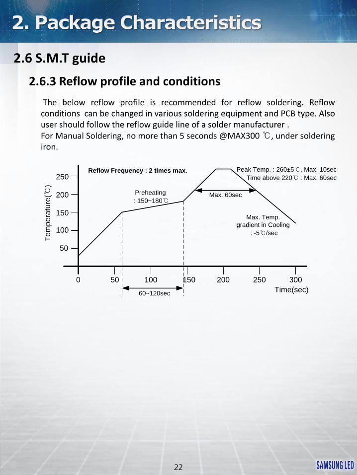
2.6 S.M.T guide
2.6.3 Reflow profile and conditions
The below reflow profile is recommended for reflow soldering. Reflow conditions can be changed in various soldering equipment and PCB type. Also user should follow the reflow guide line of a solder manufacturer . For Manual Soldering, no more than 5 seconds @MAX300 ℃, under soldering iron.
50
100
150
200
250
Te
mp
era
ture
(℃)
0 50 100 150 200 250 300
Time(sec)60~120sec
Preheating
: 150~180℃Max. 60sec
Max. Temp.
gradient in Cooling
: -5℃/sec
Peak Temp. : 260±5℃, Max. 10sec
Time above 220℃ : Max. 60secReflow Frequency : 2 times max.

23
2.7 Mechanical consideration
Please use tweezers to grab LM231A at the base. Do not touch the silicon mold side with the tweezers or fingers and the maximum compressing force is 15N on the silicone mold compound. Also don’t place pressure on the encapsulation resin – phosphor.
Correct Handling
Incorrect Handling
2.7.1 Handling guide

Samsung Kitting-Bin is purposed to maximize effective utilization in the production of Lighting applications. It is convenient to assemble LED modules in according to kitting-bin guide line. For more information about kitting bin operation, refer to LM231A datasheet.
[ 5000K, 5700K 6500K Sub-bin ]
[ 2700K, 3000K 3500K, 4000K Sub-bin ]
[SMT Pairing on board]
VE
V3
VE
V3
VE
V3
VE
V3
V3
VE
V3
VE
V3
VE
V3
VE
3.1 Kitting bin solution
3.1.1 Array solution for color uniformity
24
[Logic example] Basic Array Methods on PCB of LEDs For target bin (green line) - Cool white : one LED in 4 upper bin(3,4,7,8) could be paired with any LED in 4 lower bins(1,2,5,6) - Warm white : one LED in 4 bins(B,C,F,G) could be paired with any LEDs in diagonal 4 bins(1,2,5,6)
pair
PCB
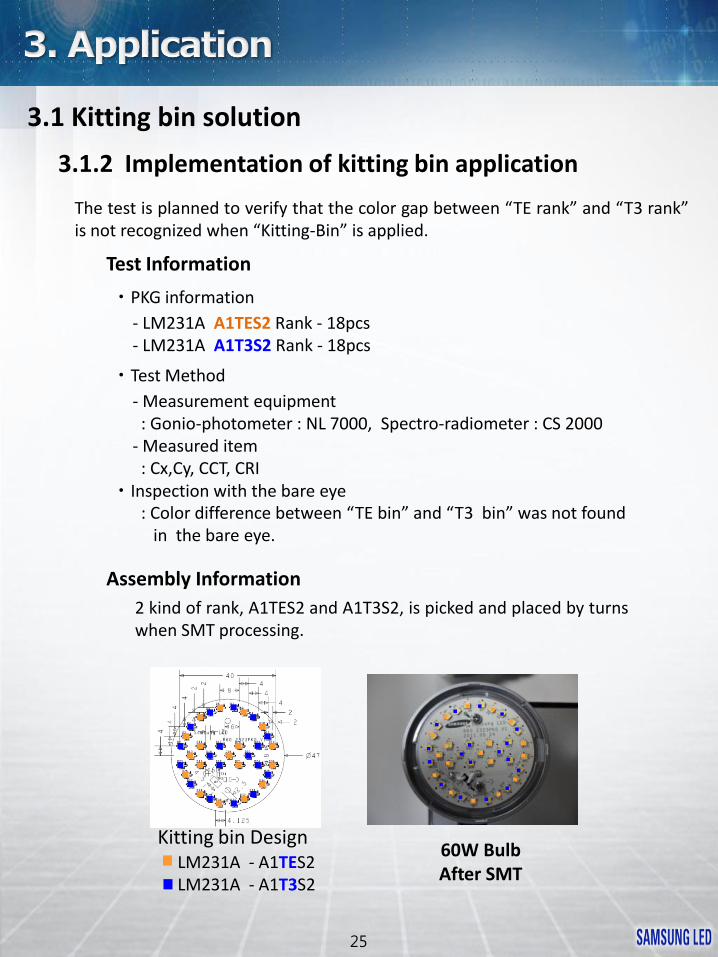
ㆍPKG information
- LM231A A1TES2 Rank - 18pcs - LM231A A1T3S2 Rank - 18pcs
ㆍTest Method
- Measurement equipment : Gonio-photometer : NL 7000, Spectro-radiometer : CS 2000 - Measured item : Cx,Cy, CCT, CRI ㆍInspection with the bare eye : Color difference between “TE bin” and “T3 bin” was not found in the bare eye.
The test is planned to verify that the color gap between “TE rank” and “T3 rank” is not recognized when “Kitting-Bin” is applied.
Test Information
LM231A - A1TES2 LM231A - A1T3S2
Kitting bin Design
3.1 Kitting bin solution
25
3.1.2 Implementation of kitting bin application
60W Bulb After SMT
Assembly Information
2 kind of rank, A1TES2 and A1T3S2, is picked and placed by turns when SMT processing.

[ Target color of bulb at chromaticity diagram ]
Target color of Bulb used “Kitting-Bin”
T1 T2
T3 T4
T5 T6 T7
T8 T9
TA
TB TC
TD TE
TF TG
26
Results
In inspection with bare eye, color difference between “TE bin” and “T3 bin” was not found out. The measured optical properties show that the color target of bulb is located within MacAdam 3 step binning.
Set Current
(A) Voltage
(Vac) Cx Cy CCT(K) CRI (Ra)
Bulb 0.065 220 0.385 0.379 3900K 83
27
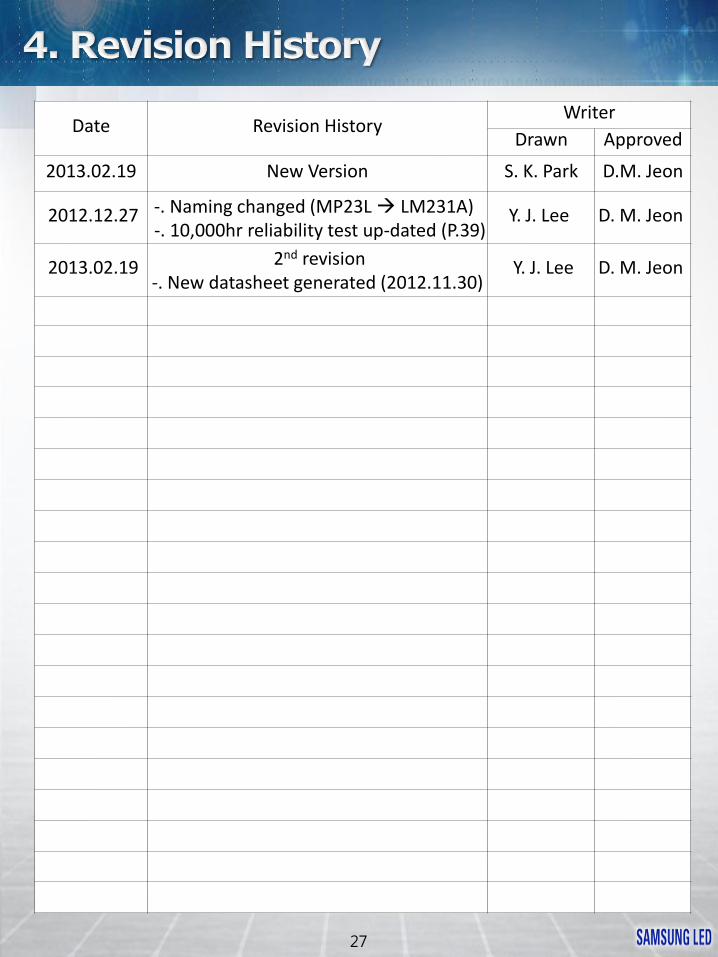
Date Revision History Writer
Drawn Approved
2013.02.19 New Version S. K. Park D.M. Jeon
2012.12.27 -. Naming changed (MP23L LM231A) -. 10,000hr reliability test up-dated (P.39)
Y. J. Lee D. M. Jeon
2013.02.19 2nd revision -. New datasheet generated (2012.11.30)
Y. J. Lee D. M. Jeon