application research at the nano and advanced materials institute
TRANSCRIPT

TTHIS ARTICLE DESCRIBES THEnanomaterials and technology applica-tion research being performed by theNano and Advanced Materials Institute(NAMI) in Hong Kong. Five focusedmarket sectors are identified where
nanomaterials and technologies canadd significant value in Hong Kongand the surrounding Pearl River Delta(PRD) region. The five areas are sus-tainable energy, display and solid-statelighting, building/construction mate-
rials, environmental technologies, andmedical and health care products.Application research undertaken byNAMI in these areas will be described.The ultimate objective of this researchis to commercialize innovative products,
Digital Object Identifier 10.1109/MNANO.2011.940949
Date of publication: 27 May 2011
P.S. CHAN, CHENMIN LIU, S.W. LIN, W.K. HO,K.W. WONG, C.Y. KWONG, K.K. HO, AND PETER W. LEE
Market-driven application research ofnanomaterials and technology.
©IN
GR
AM
PU
BLI
SH
ING
1932-4510/11/$26.00©2011IEEE JUNE 2011 | IEEE NANOTECHNOLOGY MAGAZINE | 13
and examples of these products will alsobe presented.
NAMI, a Hong Kong government-funded nonprofit company hosted bythe Hong Kong University of Scienceand Technology, was set up in 2006to conduct market-driven applicationresearch of nanomaterials and technol-ogy and also develop infrastructure anda platform in Hong Kong that can leadto a wide spectrum of innovative prod-ucts. Even though NAMI is located inand hosted by the Hong Kong Univer-sity of Science and Technology, its mis-sion is very different from a typicaluniversity. Instead of focusing on funda-mental research, NAMI aims at con-ducting market demand-led applicationresearch that can lead to market-com-petitive products in a relatively shorttime to benefit the local PRD commu-nity. NAMI collaborates with all themajor academia in Hong Kong to prolif-erate their technologies to the market-place. A substantial part of NAMI’sproject funding, roughly 40%, is fromindustrial partners. These industrial part-ners are mostly not only from HongKong and the PRD areas but also includesome international companies aiming atentering the local Hong Kong and Chi-nese markets with innovative products.
Five key market areas are targetedin NAMI’s technology roadmap. Theyinclude
u sustainable energyu display and solid-state lightingu building/construction materialsu environmental technologiesu medical and health-care products.These are the biggest market sectors in
the PRD regions to which nanomaterialsand technologies can add market-chang-ing competitiveness. Industrial partnerssponsor projects either individually in col-laborative projects or with multiple part-ners in platform projects. We will discussthe highlights of NAMI’s key technolo-gies in these areas.
SUSTAINABLE ENERGY RESEARCHAND THIN-FILM PHOTOVOLTAICPhotovoltaic (PV) is the most heavilyinvested area in NAMI’s advanced andnanomaterial research. Sustainable ener-gy research is essential to the development
of affordable and perpetual energy resour-ces for our present and future generations.It also helps to alleviate global warming byreducing green house gas emission fromcombustion of fossil fuel. Even thoughthe initial push for PV energy was fromdeveloped countries in Europe, followedby North America, China has become thefastest growing region in this area and ispoised to be in the leading PV market.China has also committed to curb 40–45%carbon emission and increase from 10% to15% the amount of total energy generatedby renewable sources by 2020. This pres-ents a big market opportunity for PVmanufacturers from Hong Kong andits surrounding PRD area.
Even though more than 80% ofworldwide PV modules installed aremade of crystalline silicon (c-Si), thin-film(TF) PV is rapidly gaining market shares.One of the main drawbacks of c-Si mod-ules is its high cost due to expensive rawmaterial, complicated manufacturing pro-cesses, and sophisticated equipment. Onthe other hand, TF PV is more promisingin achieving grid parity because of thelower costs in per watt basis, especially onthe much lower use of the critical light-absorbing materials. NAMI is currentlyconducting PV research on three majorTF technologies, namely amorphous sili-con (a-Si), copper indium gallium disele-nide (CIGS), and organic photovoltaic(OPV). The research focuses on the keysto fabricate low-cost TF solar cell, whichinclude controlling the microstructure,morphology, and composition of the TFsand their interfaces. These solar technolo-gies are complementary rather than exclu-sive to each other. Each fulfills the differentrequirements from different markets,applications, and regions. In addition, thecritical mass created by this solar researchwill help generate more opportunities inthe technical industries in Hong Kong.
Based on the study conducted by theElectrical and Mechanical Services Depart-ment of Hong Kong and the consultingfirm CDM in early 2000, solar PV wasselected as one of the few viable renew-able energy sources for Hong Kong.NAMI aims to help the Hong Kong solarindustry manufacture TF PV productsthat will not only encourage the use ofrenewable energy in Hong Kong but also
give fresh impetus to the solar industry inMainland China.
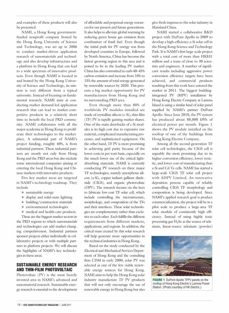
NAMI started a collaborative R&Dproject with DuPont Apollo in 2009 todevelop a high-efficiency a-Si solar cell inthe Hong Kong Science and TechnologyPark. It is NAMI’s first large-scale projectwith a total cost of more than HK$31million and a team of close to 30 scien-tists and engineers. A number of signifi-cant results including aggressive powerconversion efficiency targets have beenachieved, and commercial productsresulting from this work have entered themarket in 2011. The biggest building-integrated PV (BIPV) installation byHong Kong Electric Company at LammaIsland is using a similar kind of solar panelsupplied by NAMI’s partner DuPontApollo. Since June 2010, the PV systemhas produced about 88,000 kWh ofelectrical power per month. Figure 1shows the PV module installed on therooftop of one of the buildings fromHong Kong Electric Company.
Among all the second-generation TFsolar cell technologies, the CIGS cell isarguably the most promising due to itshigher conversion efficiency, lower toxic-ity, and lower cost of manufacturing thana-Si and Cd-Te cells. NAMI has started alarge-scale CIGS TF solar cell projectwith ADPV Limited. An innovativedeposition process capable of reliablycontrolling CIGS TF morphology andcomposition is being developed. SinceNAMI’s applied research goal is productcommercialization, the project will be in apilot scale to produce a large-area TFsolar module of consistently high effi-ciency. Instead of using highly toxicprocessing gas H2Se as the source of sele-nium, linear-source selenium (powder)
FIGURE 1 DuPont Apollo TFPV panels on therooftop of Hong Kong Electric’s Lamma PowerStation. (Photo courtesy of HK Electric.)
14 | IEEE NANOTECHNOLOGY MAGAZINE | JUNE 2011
evaporation will be used. Large areapurge flow control evaporation chamberwill be designed in conjunction withadvanced rapid thermal process and pre-cise chemical bath deposition of barrierlayer for large area uniformity control.
NAMI is also developing a third-generation TF technology—the organicPV cell fabricated by a roll-to-roll process.Although the conversion efficiency ofOPV is still low, it has a high potential tobring affordable solar energy to differentmarkets as it involves simple processingand equipment. High purity phenyl-C60-butyric-acid (PCBM) and low-costnovel donor materials will be evaluated.Process optimization concentrates oncontrolling the microstructure morphol-ogy and composition for maximizingconversion efficiency. Besides conversionefficiency improvement, NAMI is alsoworking on the reliability of the OPV cell.Again, low-cost manufacturing is theultimate goal, and a pilot roll-to-rollmanufacturing line will be established todemonstrate feasible commercial OPVproducts in the marketplace.
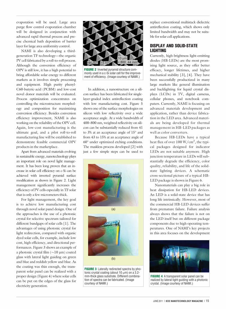
Apart from advanced materials evolvingin sustainable energy, nanotechnology playsan important role on novel light manage-ment. It has been long proven that an in-crease in solar cell efficiency on c-Si can beachieved with inverted pyramid surfacemodification as shown in Figure 2. Lightmanagement significantly increases theefficiency of PV cells especially in TF solarthat is only a few micrometers thick.
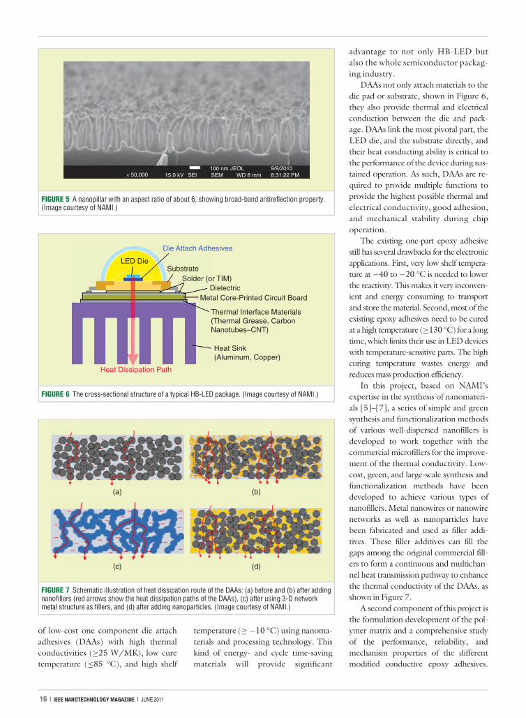
For light management, the key goalis to achieve low manufacturing costthrough novel solar panel design. One ofthe approaches is the use of a photoniccrystal for selective spectrum tailored fordifferent bandgaps of solar cells [1]. Theadvantages of using photonic crystal forlight redirection, compared with organicdyed solar cells, for example, include lowcost, high efficiency, and directional per-formances. Figure 3 shows an example ofa photonic crystal film (�10 lm) coatedglass with lateral light guiding on greenand blue and reddish yellow and blue. Asthe coating was thin enough, the trans-parent solar panel can be realized with aproper design (Figure 4) where solar cellscan be put on the edges of the glass forelectricity generation.
In addition, a nanostructure on a sili-con surface has been fabricated for single-layer-graded index antireflection coatingwith low manufacturing cost. Figure 5shows one of the surface morphologies onsilicon with low reflectivity over a wideacceptance angle. At a wide bandwidth of400–800 nm, weighted reflectivity on sili-con can be substantially reduced from 41to 3% at an acceptance angle of 15� andfrom 43 to 15% at an acceptance angle of60� under optimized etching conditions.The maskless process developed [2] withjust a few simple steps can be used to
replace conventional multistack dielectricantireflection coating, which shows onlylimited bandwidth and may not be suita-ble for solar cell applications.
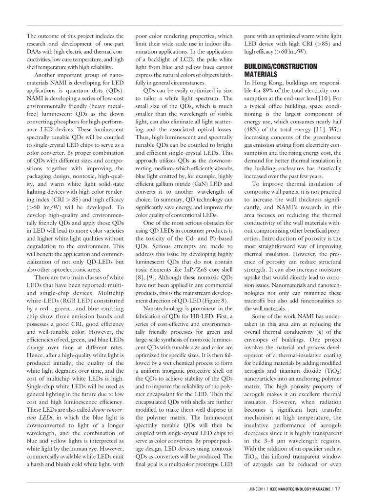
DISPLAY AND SOLID-STATELIGHTINGCurrently, high-brightness light-emittingdiodes (HB-LEDs) are the most prom-ising light source, as they offer betterefficacy, longer lifetimes, and highermechanical stability [3], [4]. They havebeen successfully productized in manylarge markets like general illuminationand backlighting for liquid crystal dis-plays (LCDs) in TV, digital cameras,cellular phones, and notebook com-puters. Currently, NAMI is focusing onadvanced materials development andapplication, rather than device fabrica-tion in the LED area. Advanced materi-als are being developed for thermalmanagement in HB-LED packages aswell as color converters.
Because HB-LEDs have a typicalheat flux of over 100 W/cm2, the typi-cal packages designed for indicatorLEDs are not suitable anymore. Highjunction temperature in LEDs will sub-stantially degrade the efficiency, colorquality, reliability, and life of the solid-state lighting devices. A schematiccross-sectional picture of a typical HB-LED package is shown in Figure 6.
Nanomaterials can play a big role inheat dissipation for HB-LED devices.An LED is a solid-state device that haslong life intrinsically. However, most ofthe commercial HB-LED devices sufferfrom premature failure. Failure analysisalways shows that the failure is not onthe LED itself but on different packagecomponents due to high operating tem-peratures. One of NAMI’s key projectsin this area focuses on the development
(a)
(b)
FIGURE 3 Laterally redirected spectra by pho-tonic crystal coating (about 10 lm) on a 3.2-mm-thick glass substrate. Different combina-tion of spectra can be fabricated. (Imagecourtesy of NAMI.)
FIGURE 4 A transparent solar panel can berealized by lateral light guiding with a photoniccrystal. (Image courtesy of NAMI.)
HKUST 15 kV10 µm× 800 44 mm
FIGURE 2 Inverted pyramid structure com-monly used in a c-Si solar cell for the improve-ment of efficiency. (Image courtesy of NAMI.)
JUNE 2011 | IEEE NANOTECHNOLOGY MAGAZINE | 15
of low-cost one component die attachadhesives (DAAs) with high thermalconductivities (�25 W/MK), low curetemperature (�85 �C), and high shelf
temperature (��10 �C) using nanoma-terials and processing technology. Thiskind of energy- and cycle time-savingmaterials will provide significant
advantage to not only HB-LED butalso the whole semiconductor packag-ing industry.
DAAs not only attach materials to thedie pad or substrate, shown in Figure 6,they also provide thermal and electricalconduction between the die and pack-age. DAAs link the most pivotal part, theLED die, and the substrate directly, andtheir heat conducting ability is critical tothe performance of the device during sus-tained operation. As such, DAAs are re-quired to provide multiple functions toprovide the highest possible thermal andelectrical conductivity, good adhesion,and mechanical stability during chipoperation.
The existing one-part epoxy adhesivestill has several drawbacks for the electronicapplications. First, very low shelf tempera-ture at�40 to�20 �C is needed to lowerthe reactivity. This makes it very inconven-ient and energy consuming to transportand store the material. Second, most of theexisting epoxy adhesives need to be curedat a high temperature (�130 �C) for a longtime, which limits their use in LED deviceswith temperature-sensitive parts. The highcuring temperature wastes energy andreduces mass production efficiency.
In this project, based on NAMI’sexpertise in the synthesis of nanomateri-als [5]–[7], a series of simple and greensynthesis and functionalization methodsof various well-dispersed nanofillers isdeveloped to work together with thecommercial microfillers for the improve-ment of the thermal conductivity. Low-cost, green, and large-scale synthesis andfunctionalization methods have beendeveloped to achieve various types ofnanofillers. Metal nanowires or nanowirenetworks as well as nanoparticles havebeen fabricated and used as filler addi-tives. These filler additives can fill thegaps among the original commercial fill-ers to form a continuous and multichan-nel heat transmission pathway to enhancethe thermal conductivity of the DAAs, asshown in Figure 7.
A second component of this project isthe formulation development of the pol-ymer matrix and a comprehensive studyof the performance, reliability, andmechanism properties of the differentmodified conductive epoxy adhesives.
Die Attach Adhesives
SubstrateLED Die
Solder (or TIM)Dielectric
Metal Core-Printed Circuit Board
Thermal Interface Materials(Thermal Grease, CarbonNanotubes–CNT)
Heat Sink(Aluminum, Copper)
Heat Dissipation Path
FIGURE 6 The cross-sectional structure of a typical HB-LED package. (Image courtesy of NAMI.)
× 50,000 15.0 kV SEI100 nm JEOLSEM WD 8 mm
9/9/20106:31:22 PM
FIGURE 5 A nanopillar with an aspect ratio of about 6, showing broad-band antireflection property.(Image courtesy of NAMI.)
(a) (b)
(c) (d)
FIGURE 7 Schematic illustration of heat dissipation route of the DAAs: (a) before and (b) after addingnanofillers (red arrows show the heat dissipation paths of the DAAs), (c) after using 3-D networkmetal structure as fillers, and (d) after adding nanoparticles. (Image courtesy of NAMI.)
16 | IEEE NANOTECHNOLOGY MAGAZINE | JUNE 2011
The outcome of this project includes theresearch and development of one-partDAAs with high electric and thermal con-ductivities, low cure temperature, and highshelf temperature with high reliability.
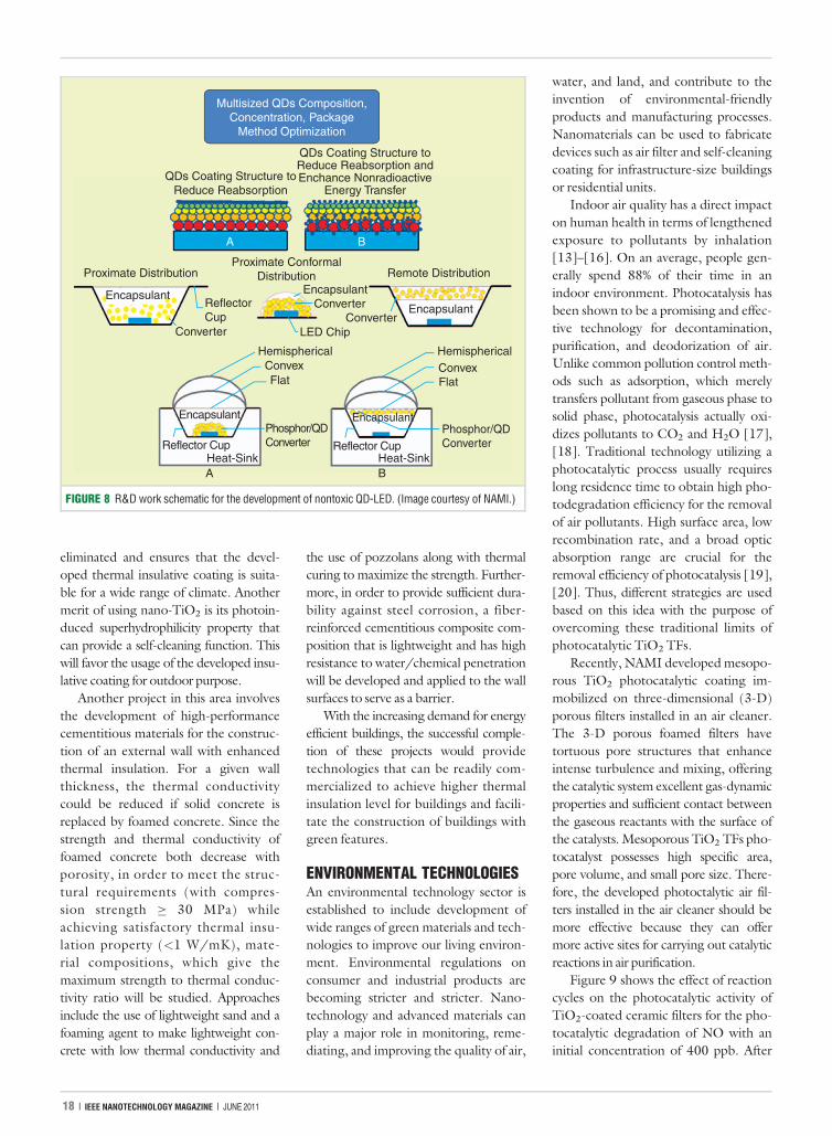
Another important group of nano-materials NAMI is developing for LEDapplications is quantum dots (QDs).NAMI is developing a series of low-costenvironmentally friendly (heavy metal-free) luminescent QDs as the downconverting phosphors for high-perform-ance LED devices. These luminescentspectrally tunable QDs will be coupledto single-crystal LED chips to serve as acolor converter. By proper combinationof QDs with different sizes and compo-sitions together with improving thepackaging design, nontoxic, high-qual-ity, and warm white light solid-statelighting devices with high color render-ing index (CRI > 85) and high efficacy(>60 lm/W) will be developed. Todevelop high-quality and environmen-tally friendly QDs and apply those QDsin LED will lead to more color varietiesand higher white light qualities withoutdegradation to the environment. Thiswill benefit the application and commer-cialization of not only QD-LEDs butalso other optoelectronic areas.
There are two main classes of whiteLEDs that have been reported: multi-and single-chip devices. Multichipwhite-LEDs (RGB LED) constitutedby a red-, green-, and blue-emittingchip show three emission bands andpossesses a good CRI, good efficiencyand well-tunable color. However, theefficiencies of red, green, and blue LEDschange over time at different rates.Hence, after a high-quality white light isproduced initially, the quality of thewhite light degrades over time, and thecost of multichip white LEDs is high.Single-chip white LEDs will be used asgeneral lighting in the future due to lowcost and high luminescence efficiency.These LEDs are also called down-conver-sion LEDs, in which the blue light isdownconverted to light of a longerwavelength, and the combination ofblue and yellow lights is interpreted aswhite light by the human eye. However,commercially available white LEDs emita harsh and bluish cold white light, with
poor color rendering properties, whichlimit their wide-scale use in indoor illu-mination applications. In the applicationof a backlight of LCD, the pale whitelight from blue and yellow hues cannotexpress the natural colors of objects faith-fully in general circumstances.
QDs can be easily optimized in sizeto tailor a white light spectrum. Thesmall size of the QDs, which is muchsmaller than the wavelength of visiblelight, can also eliminate all light scatter-ing and the associated optical losses.Thus, high luminescent and spectrallytunable QDs can be coupled to brightand efficient single-crystal LEDs. Thisapproach utilizes QDs as the downcon-verting medium, which efficiently absorbsblue light emitted by, for example, highlyefficient gallium nitride (GaN) LED andconverts it to another wavelength ofchoice. In summary, QD technology cansignificantly save energy and improve thecolor quality of conventional LEDs.
One of the most serious obstacles forusing QD LEDs in consumer products isthe toxicity of the Cd- and Pb-basedQDs. Serious attempts are made toaddress this issue by developing highlyluminescent QDs that do not containtoxic elements like InP/ZnS core shell[8], [9]. Although these nontoxic QDshave not been applied in any commercialproducts, this is the mainstream develop-ment direction of QD-LED (Figure 8).
Nanotechnology is prominent in thefabrication of QDs for HB-LED. First, aseries of cost-effective and environmen-tally friendly processes for green andlarge-scale synthesis of nontoxic lumines-cent QDs with tunable size and color areoptimized for specific sizes. It is then fol-lowed by a wet chemical process to forma uniform inorganic protective shell onthe QDs to achieve stability of the QDsand to improve the reliability of the poly-mer encapsulant for the LED. Then theencapsulated QDs with shells are furthermodified to make them well disperse inthe polymer matrix. The luminescentspectrally tunable QDs will then becoupled with single-crystal LED chips toserve as color converters. By proper pack-age design, LED devices using nontoxicQDs as converters will be produced. Thefinal goal is a multicolor prototype LED
pane with an optimized warm white lightLED device with high CRI (>85) andhigh efficacy (>60 lm/W).
BUILDING/CONSTRUCTIONMATERIALSIn Hong Kong, buildings are responsi-ble for 89% of the total electricity con-sumption at the end-user level [10]. Fora typical office building, space condi-tioning is the largest component ofenergy use, which consumes nearly half(48%) of the total energy [11]. Withincreasing concerns of the greenhousegas emission arising from electricity con-sumption and the rising energy cost, thedemand for better thermal insulation inthe building enclosures has drasticallyincreased over the past few years.
To improve thermal insulation ofcomposite wall panels, it is not practicalto increase the wall thickness signifi-cantly, and NAMI’s research in thisarea focuses on reducing the thermalconductivity of the wall materials with-out compromising other beneficial prop-erties. Introduction of porosity is themost straightforward way of improvingthermal insulation. However, the pres-ence of porosity can reduce structuralstrength. It can also increase moistureuptake that would directly lead to corro-sion issues. Nanomaterials and nanotech-nologies not only can minimize thesetradeoffs but also add functionalities tothe wall materials.
Some of the work NAMI has under-taken in this area aim at reducing theoverall thermal conductivity (k) of theenvelopes of buildings. One projectinvolves the material and process devel-opment of a thermal-insulative coatingfor building materials by adding modifiedaerogels and titanium dioxide (TiO2)nanoparticles into an anchoring polymermatrix. The high porosity property ofaerogels makes it an excellent thermalinsulator. However, when radiationbecomes a significant heat transfermechanism at high temperature, theinsulative performance of aerogelsdecreases since it is highly transparentin the 3–8 lm wavelength regions.With the addition of an opacifier such asTiO2, this infrared transparent windowof aerogels can be reduced or even
JUNE 2011 | IEEE NANOTECHNOLOGY MAGAZINE | 17
eliminated and ensures that the devel-oped thermal insulative coating is suita-ble for a wide range of climate. Anothermerit of using nano-TiO2 is its photoin-duced superhydrophilicity property thatcan provide a self-cleaning function. Thiswill favor the usage of the developed insu-lative coating for outdoor purpose.
Another project in this area involvesthe development of high-performancecementitious materials for the construc-tion of an external wall with enhancedthermal insulation. For a given wallthickness, the thermal conductivitycould be reduced if solid concrete isreplaced by foamed concrete. Since thestrength and thermal conductivity offoamed concrete both decrease withporosity, in order to meet the struc-tural requirements (with compres-sion strength � 30 MPa) whileachieving satisfactory thermal insu-lation property (<1 W/mK), mate-rial compositions, which give themaximum strength to thermal conduc-tivity ratio will be studied. Approachesinclude the use of lightweight sand and afoaming agent to make lightweight con-crete with low thermal conductivity and
the use of pozzolans along with thermalcuring to maximize the strength. Further-more, in order to provide sufficient dura-bility against steel corrosion, a fiber-reinforced cementitious composite com-position that is lightweight and has highresistance to water/chemical penetrationwill be developed and applied to the wallsurfaces to serve as a barrier.
With the increasing demand for energyefficient buildings, the successful comple-tion of these projects would providetechnologies that can be readily com-mercialized to achieve higher thermalinsulation level for buildings and facili-tate the construction of buildings withgreen features.
ENVIRONMENTAL TECHNOLOGIESAn environmental technology sector isestablished to include development ofwide ranges of green materials and tech-nologies to improve our living environ-ment. Environmental regulations onconsumer and industrial products arebecoming stricter and stricter. Nano-technology and advanced materials canplay a major role in monitoring, reme-diating, and improving the quality of air,
water, and land, and contribute to theinvention of environmental-friendlyproducts and manufacturing processes.Nanomaterials can be used to fabricatedevices such as air filter and self-cleaningcoating for infrastructure-size buildingsor residential units.
Indoor air quality has a direct impacton human health in terms of lengthenedexposure to pollutants by inhalation[13]–[16]. On an average, people gen-erally spend 88% of their time in anindoor environment. Photocatalysis hasbeen shown to be a promising and effec-tive technology for decontamination,purification, and deodorization of air.Unlike common pollution control meth-ods such as adsorption, which merelytransfers pollutant from gaseous phase tosolid phase, photocatalysis actually oxi-dizes pollutants to CO2 and H2O [17],[18]. Traditional technology utilizing aphotocatalytic process usually requireslong residence time to obtain high pho-todegradation efficiency for the removalof air pollutants. High surface area, lowrecombination rate, and a broad opticabsorption range are crucial for theremoval efficiency of photocatalysis [19],[20]. Thus, different strategies are usedbased on this idea with the purpose ofovercoming these traditional limits ofphotocatalytic TiO2 TFs.
Recently, NAMI developed mesopo-rous TiO2 photocatalytic coating im-mobilized on three-dimensional (3-D)porous filters installed in an air cleaner.The 3-D porous foamed filters havetortuous pore structures that enhanceintense turbulence and mixing, offeringthe catalytic system excellent gas-dynamicproperties and sufficient contact betweenthe gaseous reactants with the surface ofthe catalysts. Mesoporous TiO2 TFs pho-tocatalyst possesses high specific area,pore volume, and small pore size. There-fore, the developed photoctalytic air fil-ters installed in the air cleaner should bemore effective because they can offermore active sites for carrying out catalyticreactions in air purification.
Figure 9 shows the effect of reactioncycles on the photocatalytic activity ofTiO2-coated ceramic filters for the pho-tocatalytic degradation of NO with aninitial concentration of 400 ppb. After
Multisized QDs Composition,Concentration, Package
Method Optimization
QDs Coating Structure toReduce Reabsorption
Proximate Distribution
Encapsulant
Encapsulant
Encapsulant
Encapsulant
Converter
ConverterConverter
LED Chip
HemisphericalConvexFlat
HemisphericalConvexFlat
ReflectorCup
Reflector Cup Reflector CupHeat-Sink Heat-Sink
Phosphor/QDConverter
Phosphor/QDConverter
Proximate ConformalDistribution Remote Distribution
QDs Coating Structure toReduce Reabsorption andEnchance Nonradioactive
Energy Transfer
A B
A B
Encapsulant
FIGURE 8 R&D work schematic for the development of nontoxic QD-LED. (Image courtesy of NAMI.)
18 | IEEE NANOTECHNOLOGY MAGAZINE | JUNE 2011
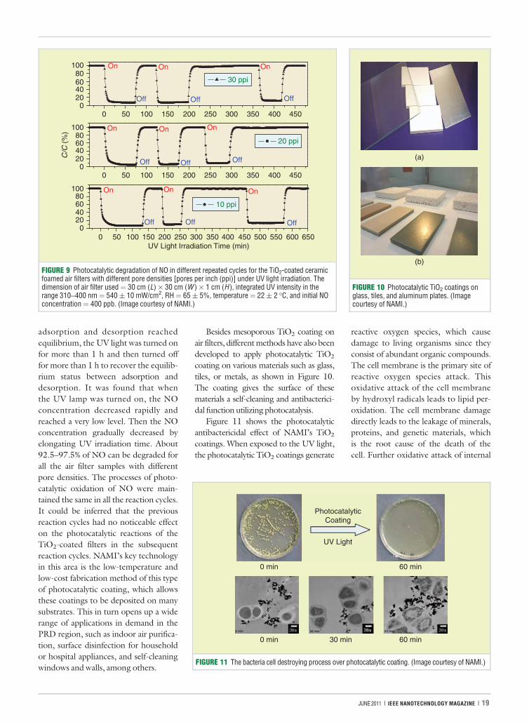
adsorption and desorption reachedequilibrium, the UV light was turned onfor more than 1 h and then turned offfor more than 1 h to recover the equilib-rium status between adsorption anddesorption. It was found that whenthe UV lamp was turned on, the NOconcentration decreased rapidly andreached a very low level. Then the NOconcentration gradually decreased byelongating UV irradiation time. About92.5–97.5% of NO can be degraded forall the air filter samples with differentpore densities. The processes of photo-catalytic oxidation of NO were main-tained the same in all the reaction cycles.It could be inferred that the previousreaction cycles had no noticeable effecton the photocatalytic reactions of theTiO2-coated filters in the subsequentreaction cycles. NAMI’s key technologyin this area is the low-temperature andlow-cost fabrication method of this typeof photocatalytic coating, which allowsthese coatings to be deposited on manysubstrates. This in turn opens up a widerange of applications in demand in thePRD region, such as indoor air purifica-tion, surface disinfection for householdor hospital appliances, and self-cleaningwindows and walls, among others.
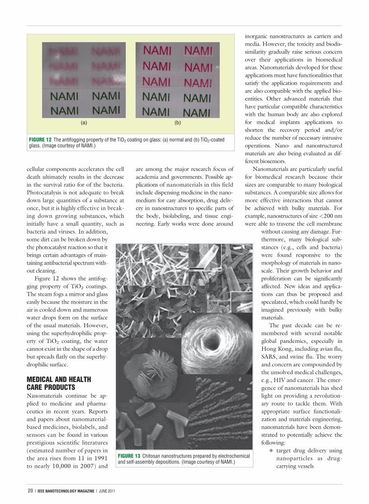
Besides mesoporous TiO2 coating onair filters, different methods have also beendeveloped to apply photocatalytic TiO2
coating on various materials such as glass,tiles, or metals, as shown in Figure 10.The coating gives the surface of thesematerials a self-cleaning and antibacterici-dal function utilizing photocatalysis.
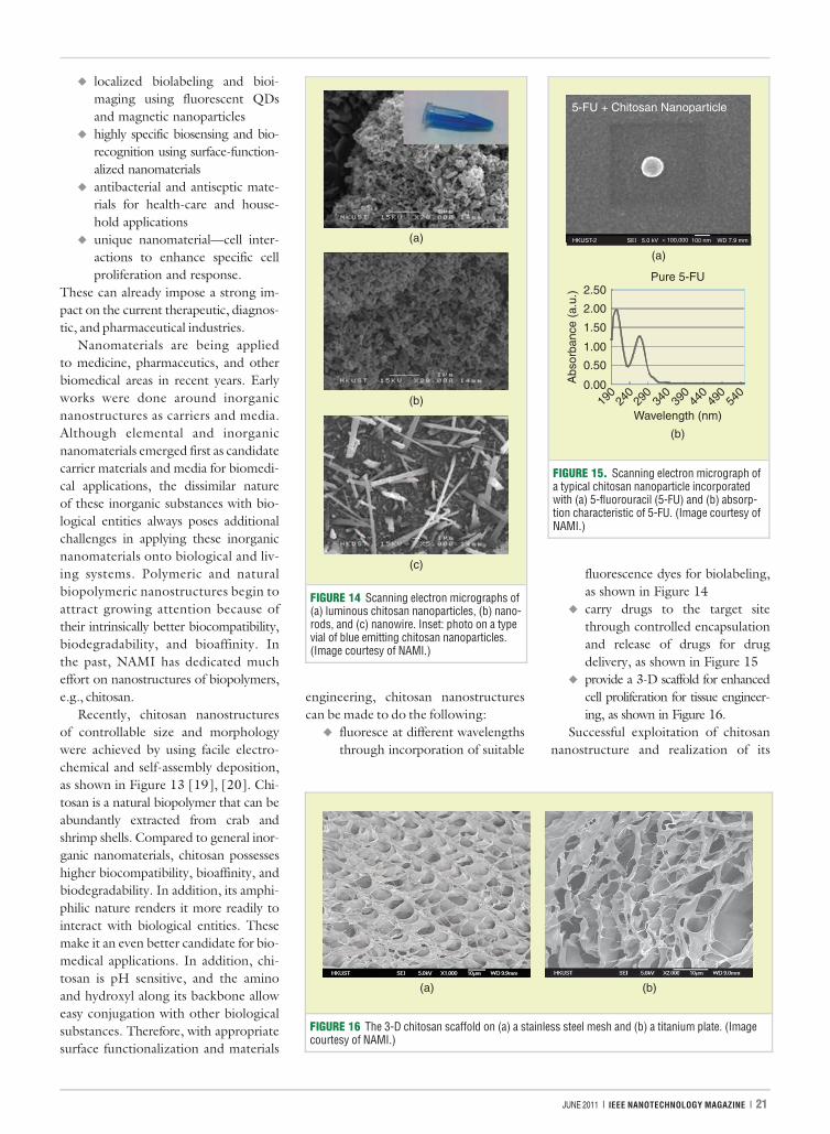
Figure 11 shows the photocatalyticantibactericidal effect of NAMI’s TiO2
coatings. When exposed to the UV light,the photocatalytic TiO2 coatings generate
reactive oxygen species, which causedamage to living organisms since theyconsist of abundant organic compounds.The cell membrane is the primary site ofreactive oxygen species attack. Thisoxidative attack of the cell membraneby hydroxyl radicals leads to lipid per-oxidation. The cell membrane damagedirectly leads to the leakage of minerals,proteins, and genetic materials, whichis the root cause of the death of thecell. Further oxidative attack of internal
(a)
(b)
FIGURE 10 Photocatalytic TiO2 coatings onglass, tiles, and aluminum plates. (Imagecourtesy of NAMI.)
PhotocatalyticCoating
UV Light
0 min 60 min
0 min 30 min 60 min
FIGURE 11 The bacteria cell destroying process over photocatalytic coating. (Image courtesy of NAMI.)
On
Off Off Off
OffOff Off
OffOffOff
On On
OnOn On
OnOnOn100806040200
0 50 100 150 200 250 300 350 400 450
100
100806040200
0 50 100 150 200 250 300 350 400 450 500 550 600 650UV Light Irradiation Time (min)
C/C
(%
) 806040200
0 50 100 150 200 250 300 350 400 450
30 ppi
20 ppi
10 ppi
FIGURE 9 Photocatalytic degradation of NO in different repeated cycles for the TiO2-coated ceramicfoamed air filters with different pore densities [pores per inch (ppi)] under UV light irradiation. Thedimension of air filter used¼ 30 cm (L) 3 30 cm (W ) 3 1 cm (H ), integrated UV intensity in therange 310–400 nm¼ 540� 10 mW/cm2, RH¼ 65� 5%, temperature¼ 22� 2 �C, and initial NOconcentration¼ 400 ppb. (Image courtesy of NAMI.)
JUNE 2011 | IEEE NANOTECHNOLOGY MAGAZINE | 19
cellular components accelerates the celldeath ultimately results in the decreasein the survival ratio for of the bacteria.Photocatalysis is not adequate to breakdown large quantities of a substance atonce, but it is highly effective in break-ing down growing substances, whichinitially have a small quantity, such asbacteria and viruses. In addition,some dirt can be broken down bythe photocatalyst reaction so that itbrings certain advantages of main-taining antibacterial spectrum with-out cleaning.
Figure 12 shows the antifog-ging property of TiO2 coatings.The steam fogs a mirror and glasseasily because the moisture in theair is cooled down and numerouswater drops form on the surfaceof the usual materials. However,using the superhydrophilic prop-erty of TiO2 coating, the watercannot exist in the shape of a dropbut spreads flatly on the superhy-drophilic surface.
MEDICAL AND HEALTHCARE PRODUCTSNanomaterials continue be ap-plied to medicine and pharma-ceutics in recent years. Reportsand papers about nanomaterial-based medicines, biolabels, andsensors can be found in variousprestigious scientific literatures(estimated number of papers inthe area rises from 11 in 1991to nearly 10,000 in 2007) and
are among the major research focus ofacademia and governments. Possible ap-plications of nanomaterials in this fieldinclude dispensing medicine in the nano-medium for easy absorption, drug deliv-ery in nanostructures to specific parts ofthe body, biolabeling, and tissue engi-neering. Early works were done around
inorganic nanostructures as carriers andmedia. However, the toxicity and biodis-similarity gradually raise serious concernover their applications in biomedicalareas. Nanomaterials developed for theseapplications must have functionalities thatsatisfy the application requirements andare also compatible with the applied bio-entities. Other advanced materials thathave particular compatible characteristicswith the human body are also exploredfor medical implants applications toshorten the recovery period and/orreduce the number of necessary intrusiveoperations. Nano- and nanostructuredmaterials are also being evaluated as dif-ferent biosensors.
Nanomaterials are particularly usefulfor biomedical research because theirsizes are comparable to many biologicalsubstances. A comparable size allows formore effective interactions that cannotbe achieved with bulky materials. Forexample, nanostructures of size<200 nmwere able to traverse the cell membrane
without causing any damage. Fur-thermore, many biological sub-stances (e.g., cells and bacteria)were found responsive to themorphology of materials in nano-scale. Their growth behavior andproliferation can be significantlyaffected. New ideas and applica-tions can thus be proposed andspeculated, which could hardly beimagined previously with bulkymaterials.
The past decade can be re-membered with several notableglobal pandemics, especially inHong Kong, including avian flu,SARS, and swine flu. The worryand concern are compounded bythe unsolved medical challenges,e.g., HIV and cancer. The emer-gence of nanomaterials has shedlight on providing a revolution-ary route to tackle them. Withappropriate surface functionali-zation and materials engineering,nanomaterials have been demon-strated to potentially achieve thefollowing:
u target drug delivery usingnanoparticles as drug-carrying vessels
(a) (b)
FIGURE 12 The antifogging property of the TiO2 coating on glass: (a) normal and (b) TiO2-coatedglass. (Image courtesy of NAMI.)
FIGURE 13 Chitosan nanostructures prepared by electrochemicaland self-assembly depositions. (Image courtesy of NAMI.)
20 | IEEE NANOTECHNOLOGY MAGAZINE | JUNE 2011
u localized biolabeling and bioi-maging using fluorescent QDsand magnetic nanoparticles
u highly specific biosensing and bio-recognition using surface-function-alized nanomaterials
u antibacterial and antiseptic mate-rials for health-care and house-hold applications
u unique nanomaterial—cell inter-actions to enhance specific cellproliferation and response.
These can already impose a strong im-pact on the current therapeutic, diagnos-tic, and pharmaceutical industries.
Nanomaterials are being appliedto medicine, pharmaceutics, and otherbiomedical areas in recent years. Earlyworks were done around inorganicnanostructures as carriers and media.Although elemental and inorganicnanomaterials emerged first as candidatecarrier materials and media for biomedi-cal applications, the dissimilar natureof these inorganic substances with bio-logical entities always poses additionalchallenges in applying these inorganicnanomaterials onto biological and liv-ing systems. Polymeric and naturalbiopolymeric nanostructures begin toattract growing attention because oftheir intrinsically better biocompatibility,biodegradability, and bioaffinity. Inthe past, NAMI has dedicated mucheffort on nanostructures of biopolymers,e.g., chitosan.
Recently, chitosan nanostructuresof controllable size and morphologywere achieved by using facile electro-chemical and self-assembly deposition,as shown in Figure 13 [19], [20]. Chi-tosan is a natural biopolymer that can beabundantly extracted from crab andshrimp shells. Compared to general inor-ganic nanomaterials, chitosan possesseshigher biocompatibility, bioaffinity, andbiodegradability. In addition, its amphi-philic nature renders it more readily tointeract with biological entities. Thesemake it an even better candidate for bio-medical applications. In addition, chi-tosan is pH sensitive, and the aminoand hydroxyl along its backbone alloweasy conjugation with other biologicalsubstances. Therefore, with appropriatesurface functionalization and materials
engineering, chitosan nanostructurescan be made to do the following:
u fluoresce at different wavelengthsthrough incorporation of suitable
fluorescence dyes for biolabeling,as shown in Figure 14
u carry drugs to the target sitethrough controlled encapsulationand release of drugs for drugdelivery, as shown in Figure 15
u provide a 3-D scaffold for enhancedcell proliferation for tissue engineer-ing, as shown in Figure 16.
Successful exploitation of chitosannanostructure and realization of its
(a) (b)
FIGURE 16 The 3-D chitosan scaffold on (a) a stainless steel mesh and (b) a titanium plate. (Imagecourtesy of NAMI.)
(a)
(b)
(c)
FIGURE 14 Scanning electron micrographs of(a) luminous chitosan nanoparticles, (b) nano-rods, and (c) nanowire. Inset: photo on a typevial of blue emitting chitosan nanoparticles.(Image courtesy of NAMI.)
5-FU + Chitosan Nanoparticle
HKUST-2 SEI 5.0 kV × 100,000 100 nm WD 7.9 mm
2.50
2.00
1.50
1.00
0.50
0.00
190
240
290
340
390
440
490
540
Wavelength (nm)
Abs
orba
nce
(a.u
.)
Pure 5-FU
(a)
(b)
FIGURE 15. Scanning electron micrograph ofa typical chitosan nanoparticle incorporatedwith (a) 5-fluorouracil (5-FU) and (b) absorp-tion characteristic of 5-FU. (Image courtesy ofNAMI.)
JUNE 2011 | IEEE NANOTECHNOLOGY MAGAZINE | 21
potential in biomedical science requiresfurther cross-disciplinary R&D involv-ing chemistry, materials science, bio-chemistry, and engineering. Despitethe challenges ahead, it is worth dedi-cating substantial and continuous efforton this area considering the enormousimpact that can be made to biomedicalscience and applications. Works on chi-tosan demonstrate the potential ofnanomaterials from natural biosubstan-ces in various aspects. R&D on othernatural biomaterials is underway atNAMI, with a goal of generating moreversatile and multifunctional nanoma-terials for biomedical and health careapplications.
CONCLUSIONThe scope of nanomaterials and tech-nologies is very wide. Different typesof advanced technology organizationsin different regions will have to choosethe kind and area of research andapplications that can reap the mostbenefits for them. NAMI has identi-fied the five market sectors in which tofocus its application research, and theoverriding objective is to develop andcommercialize innovative products tobenefit the local Hong Kong and PRDregions.
ABOUT THE AUTHORSP.S. Chan ([email protected]) re-ceived the Ph.D. degree in electronicengineering in 2006 from the Chi-nese University of Hong Kong(CUHK). She joined NAMI in 2009and is a member of the IEEE Pho-tonic Society and the Optical Societyof America.
Chenmin Liu ([email protected]) received her Ph.D. degree witha major in material science from BeijingUniversity of Aeronautics and Astronautics
in March 2005. She is an assistanttechnical manager at NAMI. She is amember of the American Chemical Soci-ety and the Singapore Chemical Society.
S.W. Lin ([email protected])received the Ph.D. degree in chemicalengineering from the Hong KongUniversity of Science and Technology.She joined NAMI in 2010 as an assist-ant technical manager.
W.K. Ho ([email protected]) is anassistant technical manager at NAMIand his research interests focus on theapplication of nanomaterials for envi-ronmental purification.
K. W. Wong. ([email protected]) is the technical manager at NAMI.He has been involved in materials andsurface analysis since 1998.
C. Y. Kwong ([email protected])received his bachelor’s, master’s, andPh.D. degrees at the University ofHong Kong in 1999, 2002, and 2005,respectively. He joined NAMI in 2008as an assistant technical manager.
K. K. Ho ([email protected]) isthe director of research and develop-ment at NAMI. He is responsible forR&D work on renewable energy andenvironmental technology.
Peter W. Lee ([email protected])received his B.S. degree in chemicalengineering and materials science fromthe University of California at Berkeleyand his Ph.D. degree in chemical engi-neering from the University of Minne-sota. He joined NAMI in October2009 as a chief technology officer aftermore than 20 years of working in thesemiconductor and photovoltaic indus-tries in the United States.
REFERENCES[1] J. Hung, P. S. Chan, C. Sun, W. H. Choi,
and W. Y. Tam, ‘‘Doubly slanted layer struc-tures in holographic gelatin emulsions: Solarconcentrators,’’ J. Opt., vol. 12, 2010.
[2] K. M. Yeung, W. C. Luk, K. C. Tam, C. Y.Kwong, M. A. Tsai, H. C. Kuo, A. M. C. Ng,and A. B. Djurisic, ‘‘2-Step self-assemblymethod to fabricate broadband omnidirectionalantireflection coating in large scale,’’ Sol.Energy Mater. Sol. Cells, vol. 95, pp. 699–703,2011.
[3] T. L. Dawson, ‘‘Development of the efficientand durable source of white light,’’ Color Tech-nol., vol. 126, pp. 1–10, 2010.
[4] Arthur D. Little Inc., ‘‘Energy saving potentialof solid state lighting in general lighting applica-tions,’’ U.S. Dept. of Energy, Rep., 2001.
[5] C. Liu, L. Guo, R. Wang, Y. Deng, H. Xu,and S. Yang, ‘‘Magnetic nanochains of metalformed by assembly of small nanoparticles,’’Chem. Commun., pp. 2726–2727, 2004.
[6] C. Liu, L. Guo, H. Xu, Z. Wu, and J. Weber,‘‘Seed-mediated growth and properties of cop-per nanoparticles, nanoparticle 1D arrays andnanorods,’’ Microelectron. Eng., vol. 66,pp. 107–114, 2003.
[7] L. Guo, C. Liu, R. Wang, H. Xu, Z. Wu, andS. Yang, ‘‘Large-scale synthesis of uniformnanotubes of a nickel complex by a solutionchemical route,’’ J. Am. Chem. Soc., vol. 126,pp. 4530–4531, 2004.
[8] E. Ryu, S. Kim, E. Jang, S. Jun, H. Jang, B.Kim, and S-W. Kim, ‘‘Step-wise synthesis ofInP/ZnS core–shell quantum dots and the roleof zinc acetate,’’ Chem. Mater., vol. 21,pp. 573–575, 2009.
[9] S. Hussain, N. Won, J. Nam, J. Bang, H.Chung, and S. Kim, ‘‘One-pot fabrication ofhigh-quality InP/ZnS (core/shell) quantumdots and their application to cellular imag-ing,’’ Chemphys. Chem., vol. 10, pp. 1466–1470, 2009.
[10] Hong Kong Environmental Protection De-partment. (2011, Apr.). Climate Change: Build-ings [Online]. Available: http://www.epd.gov.hk/epd/english/climate_change/bldg.html
[11] Environmental Bureau, Electrical andMechanical Services Department, Hong KongSAR Government, ‘‘Consultation paper: Aproposal on the mandatory implementation ofthe building energy codes,’’ 2008.
[12] Hong Kong Observatory. (2011, Apr.).Climate of Hong Kong [Online]. Available:http://www.weather.gov.hk/cis/climahk_e.htm
[13] M. De, O. S. Ghosh, and V. M. Rotello,‘‘Applications of nanoparticles in biology,’’Adv. Mater., vol. 20, pp. 4225–4241, 2008.
[14] Available: http://www.zyvex.com/nanotech/feynman.html
[15] G. Binnig, H. Rohrer, Ch. Gerber, and E.Weibel, ‘‘Surface studies by scanning tunnelingmicroscopy,’’ vol. 49, no. 1, pp. 57–1982.
[16] H. W. Kroto, J. R. Heath, S. C. O’Brien, R.F. Curl, and R. E. Smalley, ‘‘C60: Buckminster-fullerene,’’ Nature, vol. 318, pp. 162–163, 1985.
[17] S. Iijima, ‘‘Helical microtubules of graphiticcarbon,’’ Nature, vol. 354, pp. 56–, 1991.
[18] J. D. Watson and F. H. C. Crick, ‘‘A struc-ture of deoxyribose nuclei acid,’’ Nature,vol. 171, p. 737, 1953.
[19] J. M. Gong, Z. J. Zhou, X. L. Hu, M. K.Wong, K. W. Wong, and Z. L. Du, ‘‘Self-assembled chitosan nanotemplates for biomi-neralization of controlled calcite nano-archi-tectures,’’ ACS Appl. Mater. Interfaces, vol. 1,p. 26, 2009.
[20] J. M. Gong, X. L. Hu, K. W. Wong, Z.Zheng, L. Yang, W. M. Lau, and R. Du,‘‘Chitosan nanostructures with controllablemorphology by a non-aqueous electrochemi-cal approach,’’ Adv. Mater., vol. 20, p. 2111,2008.
High-brightness light-emitting diodes are themost promising light source.
22 | IEEE NANOTECHNOLOGY MAGAZINE | JUNE 2011