applications of vapor deposition in microelectronics and
TRANSCRIPT

Applications of Vapor Deposition in Microelectronics and Dye-Sensitized Solar Cells
CitationWang, Xinwei. 2012. Applications of Vapor Deposition in Microelectronics and Dye-Sensitized Solar Cells. Doctoral dissertation, Harvard University.
Permanent linkhttp://nrs.harvard.edu/urn-3:HUL.InstRepos:9826895
Terms of UseThis article was downloaded from Harvard University’s DASH repository, and is made available under the terms and conditions applicable to Other Posted Material, as set forth at http://nrs.harvard.edu/urn-3:HUL.InstRepos:dash.current.terms-of-use#LAA
Share Your StoryThe Harvard community has made this article openly available.Please share how this access benefits you. Submit a story .
Accessibility

© 2012 - Xinwei Wang
All rights reserved.

iii
Dissertation advisor Author
Professor Roy G. Gordon Xinwei Wang
Applications of Vapor Deposition in Microelectronics and Dye-sensitized
Solar Cells
Abstract
Over the past decades, vapor deposition of thin films has gained wide interest in both industry and
academia, and a variety of its applications have been demonstrated. As one of the most promising vapor
deposition techniques, atomic layer deposition (ALD) and its applications in microelectronics and dye-
sensitized solar cells are extensively investigated in this dissertation. ALD has many distinct features
including low temperature processing, self-limiting growth, and precise control of film composition and
thickness. Thus, ALD is considered to be suitable for conformal coating of 3D nanostructures, such as
nanoporous structures, high aspect-ratio trench or hole structures, and so forth. Additionally, pulsed
chemical vapor deposition (CVD) and its applications in microelectronics are explored in this dissertation.
Ruthenium (Ru) is a promising electrode material for next generation microelectronic devices. The
ALD and pulsed CVD processes discussed in Chapter 2 provide several approaches to produce smooth,
conformal, pin-hole free Ru metal thin films. High-quality Ru films can be made under either oxidizing
ambient or reducing ambient, which provides more flexibility for applications in microelectronics.
Conductive ruthenium dioxide (RuO2) is also considered as a promising microelectrode material. Chapter
3 demonstrates a pulsed CVD process of depositing pure, smooth RuO2 films with reasonably low

iv
resistivity. Chapter 3 also demonstrates that RuO2 can be epitaxially grown on rutile TiO2(011) with a
high-quality coherent heteroepitaxy structure.
III-V MOSFET is now a very active area of growing interest to researchers and engineers in electronic
industry and academia. Applications of ALD WN and high-k oxide materials for GaAs and GaN based
devices are investigated in Chapters 4 and 5. Taking advantage of the conformal-coating feature of ALD,
a stack of gate dielectric and metal gate can be coated uniformly around suspended nanowire structures,
which is crucial for well-behaved gate-all-around MOSFETs. III-V MOSFETs also generally lack a suitable
dielectric layer that has low interface trap density (Dit). Epitaxial ALD high-k dielectric lanthanum yttrium
oxide, grown on GaAs(111)A, is found to have a fairly low Dit, and therefore, the electrical properties are
dramatically improved with its inclusion. This finding is very insightful for the applications of next
generation III-V MOSFETs. In addition, a few ALD processes of candidate dielectric materials for GaN
based devices are discussed.
Dye-sensitized solar cells have great potential to compete with conventional p-n junction solar cells
due to their relatively low cost. However, their efficiency is limited by the ease with which electrons
collected by the nanoparticle framework can recombine with ions in solution. As discussed in Chapter 6,
by depositing insulating and transparent SiO2 selectively onto the open areas of nanoparticulate TiO2
surface, while avoiding any deposition of SiO2 over or under the organic dye molecules, the solar cell
efficiency can be significantly improved.

v
Acknowledgments
First and foremost, I would like to present my sincere appreciation to my advisor Prof. Roy G. Gordon
for his support, patience and encouragement throughout my PhD life at Harvard. Roy’s enthusiasm and
passion in pursuing science has always been an inspiration to me. He is always very kind to share with
me his broad knowledge and experience in chemistry, physics, materials science and electronics. I have
benefited tremendously from a great number of instructive discussions with Roy over the past four
years.
I would also like to present my great appreciation to Prof. Frans Spaepen and Prof. Michael J. Aziz for
their great support over the past years. In particular, during the past two graduate advising committee
(GAC) meetings, Frans and Michael provided me plenty of insightful suggestions and comments on my
research, without which this thesis would not have been completed. In addition, Frans taught my first
course at Harvard (i.e. AP 282), which was found the most useful course for the following research.
I am grateful for working with all the previous and current Gordon Group members. In particular, I
would like to thank Dr. Hongtao Wang for mentoring me in the first a few months since I joined this
group. I am also indebted to Dr. Zhefeng Li, Dr. Sheng Xu, and Dr. Yiqun Liu for their invaluable support
and advice during my early years in this group. My appreciation also goes to Dr. Huazhi Li, Dr. Jun-Jieh
Wang, Dr. Youbo Lin, Dr. Harish B. Bhandari, Dr. Bin Xi, Dr. Yeung (Billy) Au, Prasert Sinsermsuksakul,
Leizhi Sun, and Jing Yang for their generous help for my research. Furthermore, I would like to
particularly thank my new collaborator, Xiabing Lou, for his diligence as a scientist. I also enjoyed
working with Dr. Jaeyeong Heo, Dr. Sang Bok Kim, Dr. Sang Woon Lee, Dr. Norifusa Satoh, Dr. Qiang
Chen, Helen Park, Lauren Hartle, Kecheng Li, Danny Chua, Ashwin Jayaraman, and Lu Sun in this group.
Finally, I would like give my special thanks to Rachel Heasley. She is very kind to help me edit this thesis.

vi
I would also like to thank a number of collaborators, Prof. Shriram Ramananthan and Dr. Yanjie Cui at
Harvard SEAS; Prof. Peide D. Ye, Jiangjiang Gu and Lin Dong at Purdue University; Prof. Tomás Palacios
and Omair I. Saadat at MIT; and Prof. Joseph T. Hupp, Dr. Ho-Jin Son and Dr. Chaiya Prasittichai at
Northwestern University. I have benefited so much from numerous informative discussions with these
collaborators who are experts in a variety of areas. In addition, I would also like to appreciate the
generous research technical support from Dr. Jiangdong Deng, Dr. Ling Xie, Adam Graham, Hao-Yu (Greg)
Lin at Harvard CNS, and Dr. Scott Speakman at MIT CMSE, as well as the administrative support from
Teri Howard and Marie Purcell.
Lastly, I would like to present my deepest thanks to my parents for their long-time remote support
over the years.

vii
Table of Contents
Chapter 1 Introduction ...................................................................................................................... 1
1.1 Overview ................................................................................................................................... 1
1.2 Atomic layer deposition (ALD) .................................................................................................. 4
1.3 Pulsed Chemical Vapor Deposition (Pulsed CVD) ..................................................................... 8
1.4 Atomic layer epitaxy (ALE) ........................................................................................................ 9
1.5 Thesis outline .......................................................................................................................... 10
1.6 References .............................................................................................................................. 12
Chapter 2 Vapor Deposition of Ruthenium ..................................................................................... 14
2.1 Introduction ............................................................................................................................ 14
2.2 ALD of Ru with O2 .................................................................................................................... 16
2.2.1 Further development of ALD Ru process ........................................................................ 16
2.2.2 Ru on W substrates ......................................................................................................... 19
2.2.3 Summary ......................................................................................................................... 25
2.3 Pulsed Chemical Vapor Deposition of Ruthenium in a Reducing Ambient ............................. 25
2.3.1 Pulsed CVD Ru process and film characterization methods ........................................... 26
2.3.2 Properties of pulsed CVD Ru films .................................................................................. 28
2.3.3 Conclusions ..................................................................................................................... 37
2.4 References .............................................................................................................................. 38
Chapter 3 Pulsed Chemical Vapor Deposition of Ruthenium Dioxide and Epitaxy Analysis ........... 39

viii
3.1 Pulsed CVD of RuO2 ................................................................................................................. 39
3.2 High quality epitaxy of RuO2 on TiO2 (011) ............................................................................. 42
3.2.1 Introduction .................................................................................................................... 42
3.2.2 Epitaxy analysis by HRXRD .............................................................................................. 44
3.2.3 Other measurements ...................................................................................................... 52
3.2.4 Conclusions ..................................................................................................................... 53
3.3 RuO2 bottom electrode for studying metal-insulator transition characteristics of VO2 ......... 54
3.3.1 Introduction .................................................................................................................... 54
3.3.2 Structural analysis of VO2 on Nb:STO and RuO2/TiO2 ..................................................... 55
3.3.3 Metal-insulator transition of VO2 on Nb:STO and RuO2/TiO2 ......................................... 58
3.3.4 XPS analysis of VO2 on Nb:STO and RuO2/TiO2 ............................................................... 60
3.3.5 Conclusions ..................................................................................................................... 64
3.4 Summary ................................................................................................................................. 64
3.5 References .............................................................................................................................. 65
Chapter 4 Applications of Atomic Layer Deposition for GaAs Based Devices ................................. 68
4.1 ALD WN for metal electrodes ................................................................................................. 68
4.2 Applications of ALD for III- V gate-all-around (GAA) nanowire MOSFETs............................... 74
4.2.1 ALD of Al2O3, LaAlO3 and WN for GAA devices ............................................................... 75
4.2.2 Device properties of GAA MOSFETs with ALD high-k oxides and ALD gate metal ......... 79
4.2.3 Summary and future prospects ...................................................................................... 89

ix
4.3 Applications of ALD high-k materials for GaAs MOSFETs ....................................................... 90
4.3.1 ALD of La2O3, Y2O3 and La2-xYxO3...................................................................................... 90
4.3.2 Epitaxy of La2O3, Y2O3 and La2-xYxO3 on GaAs (111)A ....................................................... 97
4.3.3 Electrical properties of La2-xYxO3/GaAs(111)A (x = 0.2 and 0.9) .................................... 106
4.3.4 Summary and future prospects .................................................................................... 110
4.4 References ............................................................................................................................ 112
Chapter 5 Vapor Deposition of High-k materials for GaN-Based HEMT Devices .......................... 114
5.1 ALD of AlN ............................................................................................................................. 115
5.2 ALD of MgO ........................................................................................................................... 122
5.3 ALD of Sc2O3 .......................................................................................................................... 126
5.4 Pulsed CVD of ScN ................................................................................................................. 136
5.5 Other oxides for GaN-based HEMT devices .......................................................................... 137
5.6 References ............................................................................................................................ 140
Chapter 6 Selective Silica Coating for Dye-sensitized Solar Cells .................................................. 143
6.1 Introduction .......................................................................................................................... 143
6.2 Experimental ......................................................................................................................... 145
6.3 Results and discussion .......................................................................................................... 148
6.4 Summary ............................................................................................................................... 156
6.5 References ............................................................................................................................ 158

1
Chapter 1 Introduction
1.1 Overview
As Milton Ohring comments in his book titled “Materials Science of Thin Films,” thin film technology
is simultaneously one of the oldest arts and one of the newest sciences.1 Dating back to the ancient
Egyptian dynasties, the early craftsmen started to make extraordinarily thin gold leaves for art by
probably the earliest thin film technology, hammering. This thinning technology has been continuously
practiced over the past several millennia, and enormous amount of artworks have been crafted with this
method. Nowadays, the traditional manual hammering has been largely replaced with more
sophisticated machine beating and rolling technology. But, amazingly, this physical-thinning-type
technology is still the prevalent approach to produce metal sheets, such as the daily-use aluminum foils.
On the other hand, not all thin films are suitable for physical thinning. Ceramics, for example, are
generally too brittle for machine rolling, and thin film coating can hardly be achieved by any physical
thinning methods. Therefore, to fabricate various types of thin films, many other modern thin film
technologies have been proposed and developed, such as electroplating, spin coating, vapor deposition,
and so forth. Aside from the technology aspect, thin film material itself is quite an enchanting subject.
As the film thickness shrinks down to the order of sub-micrometers, many of the material properties,
such as catalytic efficiency, mechanical strength, optical, electrical and magnetic properties, etc., start to
deviate from their bulk counterparts.1 Meanwhile, quite a few fascinating small-scale phenomena start
to become pronounced, especially when the film thickness approaches the order of nanometers.
Quantum tunneling is a good example of this, as it is only observable when the thickness of the barrier
layer reaches roughly 1 nm. A straightforward and intriguing application of this is to create new artificial
materials that consist of multilayers of nanometer thin films but carry additional useful functionality.2
Tremendous achievements have been accomplished in a variety of fields by taking advantage of these
2
unique properties of thin films. For example, in microelectronics and optoelectronics, thin film
technology has been proven to be essential by its explosive growth in the applications of
communications, information processing, storage, and display. These applications have dramatically
impacted our daily lives, and they are certainly the major driving force for the development of current
thin film technology.
As one of the modern thin film fabrication methods, vapor deposition has been playing an important
role in thin film technology for over a century. Compared with solution based methods, one of the
distinct features of vapor deposition is that it can avoid the formation of bubbles and voids in the films,
so that a smooth, dense and void-free film is easier to achieve. Vapor deposition is generally classified
into two categories: physical vapor deposition (PVD) and chemical vapor deposition (CVD). Typical PVD
processes include electron beam evaporation (EE), thermal evaporation (TE), sputtering, pulsed laser
deposition (PLD), and so forth. The common feature of these PVD methods is that only pure physical
processes are involved; films are deposited from the condensation of a vapor that consists of the
desired film material. On the other hand, CVD utilizes the chemical reactions occurring at the substrate
surface to produce films. CVD also has many variants, including atmospheric pressure (APCVD), low-
pressure (LPCVD), plasma-enhanced (PECVD), and laser-enhanced (LECVD) chemical vapor deposition. In
addition, there is a special vapor deposition process called atomic layer deposition (ALD), which also
utilizes the surface chemical reactions but in a rather different way. Contrary to CVD, which supplies the
metal precursor and the co-reactant gas simultaneously into the reactor chamber, ALD supplies the
metal precursor and the co-reactant gas in an alternating sequence. As will be discussed in the next
section, this alternating-delivery feature of ALD results in many unique features, such as smooth surface
morphology, full film coverage, high conformality, etc. Indeed, ALD was considered as a variant of CVD
when it was invented. However, due to many of its unique features, it has been widely applied in rather
different areas with respect to other conventional CVD processes. Therefore, ALD is now commonly

3
accepted as a special category of deposition in the vapor deposition community. Over the past decade,
especially during the past several years, there have been numerous applications of ALD particularly in
microelectronics.3, 4 As the microelectronics industry is one of the strongest technological drivers of our
economy, it boosts the follow-up research in this field. In this thesis, we continue exploring new
applications of ALD-based deposition technology in microelectronics. But as one might have noticed, we
used the term “vapor deposition,” rather than simply ALD, in the title of this thesis. This is because
during our research, we found that for some applications, neither ALD nor conventional CVD were able
to accomplish the deposition goals. With some modifications of the deposition process, good quality
films were successfully obtained, however, the modified deposition process no longer belongs to ALD or
CVD. One example is pulsed CVD, which will be discussed in detail in the following section. Unlike
conventional CVD, pulsed CVD only keeps the co-reactant gas flowing, but delivers the metal precursor
in a pulse mode, which resembles the alternating feature of ALD to some extent. An even more
complicated case is a process consisting of hybrid features of ALD and CVD, to be discussed in Chapter 2.
But the bottom line is that these modified processes did give us good quality films, and we believe this
will bring some new insights into the development of process designing.
In addition, solar energy harvesting is another important subject for the current research society. As
the population on the earth keeps increasing, our demand for energy also increases steeply. Solar
energy is considered to be a promising candidate to solve this energy crisis, as it is not only huge in
amount, but also renewable. Unfortunately, the state-of-the-art technology is still not able to give
satisfying economically favorable products. The current solar cells are either too expensive for large-
scale manufacturing or too low in light harvesting efficiency. Therefore, high-efficiency solar cells with
low cost are still greatly in need. We explore, to some extent, the applications of ALD in one popular
type of solar cell, i.e. dye-sensitized solar cells, in the last chapter. The research in this field is generally

4
in its early stages, as many problems are still unsolved. We hope the results presented in this thesis will
provide some valuable insights.
1.2 Atomic layer deposition (ALD)
Atomic layer deposition (ALD) is an advanced thin film deposition technique for various applications
in research and industry. This technique has been reviewed many times in the past, and very recently
quite a few extensive reviews have been published as well.3, 5-12 Contrary to CVD, which allows the
precursors react at the same time on the surface, an ALD process proceeds in a cyclic manner and within
each cycle the precursors are separately supplied in an alternating sequence. An ideal ALD growth cycle
typically includes the following steps:
(1) Expose the substrate surface to Precursor A and allow the surface reaction with Precursor A to
go to completion;
(2) Purge with inert gas to remove excess Precursor A and the byproducts of the surface reaction;
(3) Expose the surface to Precursor B and allow the surface reaction with Precursor B to go to
completion;
(4) Purge with inert gas to remove excess Precursor B and the byproducts of the surface reaction.
Ideally, the surface reactions involved in Steps (2) and (4) should be self-limiting, so that only one (or
a certain portion of a) monolayer of material is deposited within each cycle. This makes ALD a fairly
controllable thin film deposition process, as the final thin film thickness can be calculated by multiplying
the growth rate (thickness grown per cycle) by the total number of cycles. Also, because of the
saturation behavior of the surface reaction, ALD offers advantages for producing smooth, uniform,
dense and conformal films. In particular, conformal film coating is a unique feature of ALD, and it is

5
always considered the most important advantage of ALD. Whatever the substrate shape is, all the
exposed surface will be uniformly coated by an ideal ALD process.
However, many ALD processes are not ideal. One of the causes of non-ideality is the self-
decomposition of the precursor. When a precursor decomposes, it usually leads to non-self-limiting
behavior of the surface chemistry, and therefore the film conformality is likely to be compromised. Also,
if the precursor contains carbon as many of the organometallic precursors do, the decomposition of a
precursor may also increase the carbon impurity level in the film. Another cause for non-ideal growth
behavior of ALD is the low reactivity of the precursor with a substrate. When this occurs, the nucleation
of the film is often delayed by many cycles, and growth happens only sporadically and non-reproducibly
on defects on the substrate. A third cause for non-ideality is that when a precursor etches or reacts with
the film, a stable saturation can hardly be reached. The above three causes are all related to the
precursor design, which is one of the major research subjects of ALD.
A good precursor for ALD should have sufficient volatility, thermal stability and self-limited reactivity,
and the precursor should not etch the substrate or the deposited film.13 A liquid precursor is more
favorable than a solid precursor, as a liquid usually has a higher and steadier vaporization rate than a
solid. In addition, from a practical point of view, an ideal precursor should be non-flammable, non-
corrosive, non-toxic, non-hazardous, and simple and inexpensive to synthesize and purify. It is generally
difficult to find ideal precursors that satisfy all of these requirements. Many efforts have been devoted
to the development of better precursors. Every year, numerous new precursors are synthesized and
tested for ALD. Popular precursors include halide, alkyl, cyclopentadienyl, alkoxide, β-diketonate, amide,
imide, and amidinate compounds.13 A thorough discussion of these precursors is out of the scope of this
thesis; please refer to recent reviews on this subject for details. But we would like to discuss the

6
amidinate family of precursors a bit more, since we will use this type of precursor multiple times in the
following chapters.
Figure 1.1. Structure of a metal amidinate precursor.
An amidinate ligand is a bidentate ligand, and it forms a chelate complex with a metal center (Figure
1.1). The chelate effect means that metal amidinates are more thermally stable than metal amides. The
physical and chemical properties of metal amidinates can be engineered by varying the alkyl groups
attached to the two nitrogen atoms in the ligand (i.e. R1 and R2 in Figure 1.1). As a general rule of thumb,
in order to obtain the highest precursor volatility, the size of the side alkyl groups needs to be just large
enough to prevent oligomerization of the compound. Alkyl groups that are too bulky would result in low
reactivity because of the crowding of the ligands around the metal center. Compared with β-diketonate
precursors which have a similar chelate structure, the ligands in the amidinates are usually better
leaving groups in depositions. This is because metal-nitrogen bonds are usually weaker than metal-
oxygen bonds and, therefore, the metal-nitrogen bonds in amidinates are easier for NH3 or H2O to attack.
Consequently, fewer leftover ligands (impurities) remain in films produced from amidinate precursors.
In the later chapters of this thesis, we use multiple amidinate precursors to deposit ruthenium,
ruthenium dioxide, lanthanum oxide, yttrium oxide, scandium oxide, and magnesium oxide thin films.
ALD is considered the best technique for conformal coating. To achieve 100% of step coverage,
enough precursor vapor exposure needs to be supplied. The minimum requirement of the vapor
exposure is determined by both the precursor reactivity and the substrate structure. The precursor
7
reactivity determines the minimum local vapor exposure required to saturate a surface reaction. A fast
surface reaction usually needs just a few Langmuir of exposure (1 Langmuir = 10-6 Torr s) to saturate (e.g.
tetrakis(dimethylamino) hafnium reacts with H2O), and the corresponding precursor is considered highly
reactive. If the minimum required exposure exceeds 1 Torr s, the precursor may be difficult (though not
impossible) to use for ALD. The substrate structure is another important factor for conformality, as it
affects the diffusion of the precursor vapor to the surface. As an example, the step coverage in deep and
narrow holes has been studied by a kinetic model by Gordon et al.14 The model takes into account the
diffusion of the reactants from the opening end of a hole and concludes that, to achieve 100% step
coverage, the minimum exposure (Emin) is:
√ [
],
where S is the saturation dosage, m is the mass of the precursor molecule, kB is the Boltzmann constant,
T is the deposition temperature, and a is the aspect ratio defined as with L, p, and A being
the depth, perimeter, and cross-section area of the hole structure, respectively. This equation conveys
an important message for system scaling, as it reveals the fact that it is only the aspect ratio of a
structure that affects the minimum exposure. A later model proposed by Kim et al. takes into account
the effect of non-unity sticking probability, and extends the model applications to the non-saturation
region of ALD.15, 16
As ALD is an atomic-level layer-by-layer growth method, the major drawback is its low growth rate. A
typical growth rate is around 0.1 nm per ALD cycle, and one cycle takes about a few to several tens of
seconds to complete. A simple calculation would give us the following estimation that a micrometer-
thick film would take a few hours or days to finish, which is too slow for mass production. Therefore,
most of the ALD applications are generally based on nanometer-thick films. One the other hand, there is

8
a branch of ALD called rapid ALD in which the growth rate can increase to more than 16 nm per cycle.17,
18 A successful example is depositing SiO2 from tris(tert-butoxy) silanol (TBOS) and trimethylaluminum
(TMA).17 In this deposition, the silanol precursor polymerizes at the catalytic Lewis-acid aluminum
centers to form nanometer-long silicon-oxygen chains with tert-butoxy groups on the side. These silicon-
oxygen chains cross link to each other, forming a silicon-oxygen network (or equivalently SiO2) through
an elimination process of the side tert-butoxy groups. This silicon-oxygen network prevents the silanol
precursor from further diffusing through to reach aluminum centers, so that the polymerization stops at
a certain stage, and therefore a self-limiting growth of nanometer-thick SiO2 layer per cycle is achieved.
Indeed, the saturated SiO2 growth rate results from a delicate balance between the steps of diffusion,
polymerization, and cross-linking, and therefore this process is somewhat difficult to operate.
Regardless, the rapid ALD process is a promising technique for many applications. We will discuss one of
its applications in dye-sensitized solar cells in the last chapter of this thesis.
1.3 Pulsed Chemical Vapor Deposition (Pulsed CVD)
Pulsed chemical vapor deposition (pulsed CVD) derives from ALD and CVD, and it has both of their
features. In a pulsed CVD process, the co-reactant gas is usually kept flowing continuously, while a metal
precursor is delivered in a pulse mode. A comparison of the ALD, CVD, and pulsed CVD processes is
illustrated in Figure 1.2. Pulsed CVD is often applied in some cases where neither ALD nor CVD can be
used. An example is depositing RuO2 from bis(N,N’-di-tert-butylacetamidinato) ruthenium(II) dicarbonyl
and O2. The deposition cannot be run by an ALD process, since the Ru amidinate precursor can reduce
RuO2 to Ru metal. Therefore, the surface reaction of oxidizing Ru amidinate to RuO2 only occurs in an O2-
excess environment. But since the Ru amidinate is a solid precursor, the continuous steady flow of the
precursor needed in CVD is difficult to achieve. Fortunately, we found that pulsed CVD with continuously
flowing O2 and pulsing Ru amidinate was able to solve both problems at the same time, and good quality
RuO2 films were obtained. Details of the process and results will be discussed in Chapter 3 of this thesis.

9
Figure 1.2. Comparison of ALD, CVD and pulsed CVD.
The surface reaction is not self-limiting in pulsed CVD, and thus the deposited film is not strictly
conformal. However, as many of CVD reactions do exhibit somewhat saturation tendency,19, 20 if the
pulsed CVD process uses the right precursor, a fairly good step-coverage may still be achieved with
careful optimization of the deposition conditions. In fact, a good step-coverage was obtained in our
pulsed CVD process of Ru metal as will be shown in Chapter 2. Also in Chapter 2, an even more
complicated process which combines ALD and pulsed CVD is used. This hybrid process is particularly
interesting when a second co-reactant gas is needed but has an antagonistic effect with the first one.
Details can be found in Section 2.3.1.
1.4 Atomic layer epitaxy (ALE)
Atomic layer epitaxy (ALE) is actually an old name for atomic layer deposition (ALD) dating back to
1980s - 1990s, because most of the research of ALD at that time was devoted to the epitaxial growth of
10
III-V semiconductors.11 Traditional precursors, such as trimethylaluminum (TMA), trimethylgallium
(TMG), trimethylindium (TMI), PH3, and AsH3, have been extensively studied for growing epitaxial layers
of AlAs, GaAs, GaAlAs, GaP, InP, and InAs.12 However, the utility of ALE of these III-V compounds has
been limited due to the relatively narrow operating temperature window, low growth rate, and the
unintentional incorporation of high levels of carbon impurities.21 Obviously, one obstacle for ALE (or ALD)
of III-V compounds is the lack of suitable precursors.
Over the decades of research, the epitaxial growth community has extended their interest to the
epitaxy of oxides, which have exhibited many peculiar and intriguing properties.22 Meanwhile, many
new metal precursors, such as transition-metal and lanthanide-metal precursors, have been developed
during the past decades.23 Therefore, we believe it is a good time to reconsider the atomic layer epitaxy
of oxides. In this thesis, we will demonstrate two cases of heteroepitaxy, RuO2 on TiO2 in Chapter 3, and
lanthanum yttrium oxide on GaAs in Chapter 4. For consistency, we will use the term ALD, not ALE, in
the following discussion.
1.5 Thesis outline
The thesis is organized in the following way:
Chapter 1 reviews the basics of the ALD process and introduces the pulsed CVD process and
the ALE process. These processes will be discussed throughout the following chapters.
Chapter 2 investigates the growth of ruthenium metal thin films by several vapor deposition
approaches. High-quality ruthenium metal films can be made not only under oxidizing
ambient but also under reducing ambient, which provides more flexibility of process for its
applications in microelectronics.
Chapter 3 is dedicated to studying the deposition of conductive RuO2 thin films. Also, high-
quality coherent heteroepitaxial growth of RuO2 on rutile TiO2 is demonstrated.
11
Chapter 4 extends the applications of ALD to GaAs based devices. Incorporating an ALD metal
layer and/or an ALD high-k oxide layer into the devices can dramatically improve the
electrical properties of the device, which is very promising for applications in next generation
III-V MOSFETs.
Chapter 5 describes the depositions of several types of oxides that are considered to be
compatible for GaN based devices.
Chapter 6 applies the rapid ALD of SiO2 to dye-sensitized solar cells, which significantly
improves the solar cell efficiency.

12
1.6 References
1 M. Ohring, Materials science of thin films (Academic press, 2002).
2 H. N. Lee, H. M. Christen, M. F. Chisholm, C. M. Rouleau, and D. H. Lowndes, Nature 433, 395
(2005).
3 L. Niinisto, J. Paivasaari, J. Niinisto, M. Putkonen, and M. Nieminen, Phys. Status Solidi A-Appl.
Res. 201, 1443 (2004).
4 C. S. Hwang, in Atomic layer deposition of nanostructured materials, edited by N. K. Pinna, Mato
(Wiley-VCH, 2012).
5 S. M. George, Chem. Rev. 110, 111 (2010).
6 C. Marichy, M. Bechelany, and N. Pinna, Adv. Mater. 24, 1017 (2012).
7 C. Bae, H. Shin, and K. Nielsch, Mrs Bulletin 36, 887 (2011).
8 W. M. M. Kessels and M. Putkonen, Mrs Bulletin 36, 907 (2011).
9 J. W. Elam, N. P. Dasgupta, and F. B. Prinz, Mrs Bulletin 36, 899 (2011).
10 M. Leskela, M. Ritala, and O. Nilsen, Mrs Bulletin 36, 877 (2011).
11 G. N. Parsons, S. M. George, and M. Knez, Mrs Bulletin 36, 865 (2011).
12 R. L. Puurunen, J. Appl. Phys. 97 (2005).
13 M. Putkonen, in Atomic layer deposition of nanostructured materials, edited by N. K. Pinna,
Mato (Wiley-VCH, 2012).
14 R. G. Gordon, D. Hausmann, E. Kim, and J. Shepard, Chem. Vapor Depos. 9, 73 (2003).
15 J. Y. Kim, J. H. Ahn, S. W. Kang, and J. H. Kim, J. Appl. Phys. 101 (2007).
16 J. Y. Kim, J. H. Kim, J. H. Ahn, P. K. Park, and S. W. Kang, J. Electrochem. Soc. 154, H1008 (2007).
17 D. Hausmann, J. Becker, S. L. Wang, and R. G. Gordon, Science 298, 402 (2002).
18 B. B. Burton, M. P. Boleslawski, A. T. Desombre, and S. M. George, Chem. Mat. 20, 7031 (2008).

13
19 A. Yanguas-Gil, N. Kumar, Y. Yang, and J. R. Abelson, Journal of Vacuum Science & Technology A
27, 1244 (2009).
20 A. Yanguas-Gil, Y. Yang, N. Kumar, and J. R. Abelson, Journal of Vacuum Science & Technology A
27, 1235 (2009).
21 M. Leskela, in Atomic layer deposition of nanostructured materials, edited by N. K. Pinna, Mato
(Wiley-VCH, 2012).
22 S. A. Chambers, Adv. Mater. 22, 219 (2010).
23 B. S. Lim, A. Rahtu, and R. G. Gordon, Nature Materials 2, 749 (2003).

14
Chapter 2 Vapor Deposition of Ruthenium
2.1 Introduction
Ruthenium (Ru) metal has many unique properties. It has a relatively high work function, its oxide,
RuO2, is conductive, and it is compatible with many oxide high-k dielectric materials, such as SrTiO31 and
TiO2.2 Hence, Ru is being considered as electrodes for dynamic random access memories (DRAM)2 and
gate metal for metal-oxide-semiconductor-field-effect (MOSFET) transistors.3 Ru can also be used as a
seed layer for electrodeposition of copper interconnects.4 Many chemical processes use ruthenium as a
catalyst.5 Preparing thin Ru film with good properties, such as high density, low resistivity, and pinhole-
free smooth surface, has raised much interest in industry recently. Vapor deposition is a promising
approach to obtain thin Ru films with high quality and uniform thickness even inside narrow features.
Several Ru compounds have been studied as precursors for atomic layer deposition (ALD) and chemical
vapor deposition (CVD). But many of them, such as Ru(Cp)2 6 and Ru(thd)3 ,
7 need to react with O2 in
order to deposit Ru films. This may cause some unwanted oxidation of conductive substrates, such as
titanium nitride in DRAM electrodes or tantalum nitride diffusion barriers in microelectronic
interconnects. Our group has synthesized an amidinate Ru precursor, bis(N,N’-di-tert-
butylacetamidinato) ruthenium(II) dicarbonyl (Figure 2.1), which can react with either NH3 or O2 to
produce Ru film by atomic layer deposition (ALD).8-10 Therefore, Ru films can be prepared in either an
oxidizing ambient or a non-oxidizing ambient with this precursor.8, 10
The ALD process of Ru with amidinate Ru precursor and NH3 is described in a published reference.8 At
300 °C deposition temperature, the ALD process produced fairly conformal and smooth crystalline Ru
films. However, this ALD process was reported to be not self-limiting: more than 50% of the film growth
was due to its CVD component, and increasing the size of the vapor doses resulted in higher growth rate.

15
The lowest Ru film resistivity value by this process was reported to be around 30 μΩ cm for a 30 nm Ru
film. Even though the authors found this resistivity value was in line with the PVD Ru, it was still higher
than the value for bulk Ru, i.e. 7.1 μΩ cm. It might be due to the carbon impurities from the CVD
component of the process. Even though the impurity level of carbon was only ~0.05% according to their
secondary ion mass spectrometry (SIMS) measurement, the carbon impurities were found to
accumulate at the Ru grain boundaries in later studies,10 which could have a pronounced effect on
electron transport.
Figure 2.1. Molecular structure of Ru precursor.
Later, an ALD process using O2, instead of NH3, as the co-reactant gas was developed in our group.10
The growth temperature was at 325 °C for a growth rate of roughly 0.1 nm per cycle. The produced Ru
films had an equal-to-bulk density of 12.3 g/cm3, and a close-to-bulk resistivity (8.6 μΩ cm v.s. 7.1 μΩ cm
for bulk Ru), with a smooth surface. Moreover, the impurity level was fairly low: according to the
reported atom probe microscopy (APM) results, both the carbon and oxygen impurity levels were
around 0.3%. This was very encouraging, as oxygen was not incorporated in the films, despite that
oxygen was used as the co-reactant. However, one issue with this ALD process was that the oxygen
dosage was found to be an extremely critical factor. There was a fairly narrow window of oxygen

16
exposure in each ALD cycle (0.02 ~ 0.04 Torr s): the film quality was good if the oxygen exposure was
within the range, but the films would have high resistance if the oxygen was under-dosed; while the
films would peel off if the oxygen was over-dosed.
In this chapter, we report some additional results of the ALD Ru process with O2, including further
process modification, and film adhesion and coverage tests (Section 2.2). Then, the deposition behavior
of this amidinate Ru precursor in chemical vapor deposition (CVD) conditions is discussed in the
following. With NH3 and H2 as the co-reactant gases, high quality Ru metal films were successfully
deposited with a specially designed pulsed CVD method (Section 2.3). As this new process was run in a
reducing ambient, it could circumvent the issue of unwanted oxidation of conductive substrates as
previously mentioned.a
2.2 ALD of Ru with O2
2.2.1 Further development of ALD Ru process
As mentioned in Section 2.1, earlier studies of ALD Ru from the amidinate Ru precursor (Figure 2.1)
and O2 showed good film quality, if the oxygen exposure in each ALD cycle was within the 0.02 ~ 0.04
Torr s range (Figure 2.2).10 The produced Ru films had density equal to the bulk value of 12.3 g/cm3, a
low resistivity (8.6 μΩ cm v.s. 7.1 μΩ cm for bulk Ru), and a relatively smooth surface (1.9 nm of rms
roughness for a 35 nm-thick film). However, if the oxygen was under-dosed, the film resistivity went up
steeply and the growth rate dropped drastically; while if the oxygen was over-dosed, the films easily
peeled off during deposition (Figure 2.3). This narrow exposure window is one of the major drawbacks
of this ALD process, as it would need ultra-precise controlling of O2 dosage for further large-scale
applications. Another issue with this process is the relatively high deposition temperature (325°C), which
could limit potential industrial applications.
a A pulsed CVD process with oxygen will be discussed in Chapter 3.

17
In order to avoid those problems mentioned above, we investigated the deposition behavior at a
lower temperature. We kept most of the deposition conditions the same as before: the ALD was carried
out in the same home-built tube reactor as before; and the Ru precursor was placed in the same glass
bubbler in an oven at the same elevated temperature as before (i.e. 140 °C), which guaranteed the
precursor delivering amount in each cycle was the same as before. The only difference we made was
lowering the deposition temperature to 300 °C. But as shown in Table 2.1, the results were noticeably
different, even though there was only a difference of 25 °C in deposition temperatures. At the lower
temperature, the film growth rate was slightly lower, and the film smoothness was better (Figure 2.4),
but the film resistivity increased by a factor of 2. The increased resistivity could be due to the smaller
grain size formed at lower deposition temperature, and the smaller grains were more effective in
scattering electrons. We also noticed that, as contrary to the high deposition temperature case, in which
the films started to peel off when the O2 exposure exceeded 0.04 Torr s, the Ru films deposited at 300 °C
adhered very well to the SiO2 substrates, even with the highest O2 exposure we could achieve in our
reactor (i.e. 0.62 Torr s). These results were encouraging to us, as they suggested a direction for
developing a better deposition recipe, which does not need precise control of the O2 to retain the good
quality of the produced films.

18
Figure 2.2. Early studies of ALD Ru with O2 (See Reference 10 for details)
Figure 2.3. SEM image of a peeled-off Ru film, when the O2 exposure was beyond the optimal range.

19
Table 2.1. Quality of Ru thin films deposited with 100 ALD cycles at 300 °C
Deposition Temperature (°C)
O2 exposure (Torr s)
Growth rate
(nm/cyc)
Resistivity
(μΩ cm)
Rms rougness
(nm)
325 (Reference) 0.04 0.102 14.0 1.9
300 0.08 0.077 31.6 2.9
300 0.10 0.072 27.5 2.8
300 0.22 0.089 23.8 2.1
300 0.40 0.093 25.0 1.7
300 0.62 0.096 25.2 1.4
Figure 2.4. AFM of a 10 nm Ru film deposited at 300 °C. The rms roughness is 1.4 nm.
2.2.2 Ru on W substrates
We further studied the Ru films deposited on tungsten (W) substrates, since W is a common
electrode material used in semiconductor industry. We were particularly interested in the following
three aspects of this Ru/W structure: (1) since oxygen was involved in the ALD process of Ru, potential

20
oxidation of the conductive W substrates and the formation of a resistive interfacial oxide layer was one
of the major concerns; (2) the adhesion of the Ru films to the partially oxidized W substrates was
another concern, as Ru was known to have poor adhesion to many oxides, e.g. Ru films deposited on
thermal SiO2 could not pass the tape test, indicating the adhesion energy was below 3 J/m2; and (3) the
surface coverage of the deposited Ru films, or the pinhole density in the Ru thin films, was another
crucial criterion to evaluate the film quality.
The W substrates were prepared by sputtering W metal onto Si wafers. The substrates were later
transferred into our ALD reactor for Ru deposition with the optimized deposition recipe as mentioned
previously. Cross-sectional TEM was used to examine the Ru/W interface. As shown in Figure 2.5, the
TEM images clearly showed no visible interfacial oxide layer, which suggested that the small amount of
oxygen dosage introduced during deposition did not cause too much oxidation on the W substrates.b
The Morié fringes in the TEM images extended throughout the entire Ru layer, suggesting that the Ru
film was well crystallized. The lateral Ru grain size was around 30 nm. Further electrical measurements
showed that the Ru film was in good electrical contact with the W substrate, as the sheet resistance
remained the same before and after depositing the Ru layer.c
b We are prone to believe that there was no interfacial oxide layer formed even though O2 was involved in the
deposition process. The reason is that the amidinate Ru precursor is a reducing agent and it can effectively reduce the surface oxide whenever it is formed in the previous O2 half-cycle in the ALD process.
c The sheet resistance of Ru/W layer was dominated by the underneath thick W layer (Figure 2.5). Same sheet
resistance suggested that no thick insulating interfacial tungsten oxide was formed.

21
Figure 2.5. Cross-sectional TEM of Ru/W. No visible WOx layer observed.
As another concern was the adhesion of Ru film to W substrates, we studied the adhesion energy of
Ru/W bilayer by the four-point bend method.11-13 Before the measurement, samples were deposited
with 0.13 μm of sputtered aluminum, and then attached by high strength epoxy (EPO-TEK 353ND from
Expoxy Technology) to a piece of dummy silicon water. The bonded wafers were cut into 50 × 5 mm
beams. Then, a notch was scribed at the center of each beam to initiate a crack. Despite the fact that Ru
does not adhere very well to many oxides, e.g. thermal SiO2 and even its own oxide RuO2, the adhesion
between Ru and W (or with a possible ultra-thin WOx layer in between) was found to be very strong
(greater than 11 J/m2).d This strong adhesion energy will guarantee that this Ru/W bilayer structure
remains undamaged after most harsh follow-up processes, such as the chemical mechanical polishing
(CMP) process.
Film coverage is another crucial criterion to evaluate film quality. A film contains a high density of
pinholes is regarded as poor quality. The worst case is that the film is island-like and essentially
d We were not able to obtain the exact value of adhesion energy, as the samples cracked at the W/SiO2
interface, as opposed to the Ru/W interface. But this suggested that the adhesion energy of Ru/W should be greater than that of W/SiO2, which was measured to be 11 J/m
2.

22
discontinuous. The Ru films deposited by our recipe clearly showed continuous film features, and no
observable pinholes by AFM (Figure 2.4) and SEM. However, it might still be possible that those films
contained tiny pinholes, which were beyond the detection limit of AFM and SEM. In order to examine
those tiny pinholes, we applied an etching approach to enlarge the pinhole size to be observable by SEM.
10% H2O2 aqueous solution was used as the etchant for detecting pinholes in the Ru films deposited on
W substrates, since the H2O2 can selectively etch away W but not Ru. If there are any pinholes passing
through the Ru films, the H2O2 etchant can go through those pinholes and attack the underneath W layer.
As a result, sub-micro-size holes will be formed in the underneath W layer, and these holes are
resolvable by SEM. This etching process is schematically illustrated in Figure 2.6. A Ru-on-W sample,
where the Ru film thickness was 7.3 nm, was immersed in the H2O2 etching solution for 10 minutes.
Then, its surface morphology was captured by SEM as shown in Figure 2.7(a). The SEM image clearly
showed that pinholes existed in the Ru film, even though they were too small to be directly observed
without the etching process. Cross-sectional TEM provided further structural information of those
etched holes. As shown in Figure 2.7(b), a hole with lateral size of 330 nm was found in the W layer after
etching, while the overlying Ru film was still intact. Also under cross-sectional TEM, no pinholes in the Ru
film were observed, perhaps because of the small size of the pinholes or simply because there were so
few pinholes that the cross-section was not likely to cut through them. Nevertheless, the cross-sectional
TEM image of an etched film showed features similar to the etched holes that were observed by SEM,
supporting that our etching method is an effective approach to detect tiny pinholes.

23
Figure 2.6. Schematic illustration of enlarging pinholes by etching.
As one of our goals was to reduce the pinhole density, and eventually achieve pinhole-free Ru films,
we further investigated a variety of surface treatments to the W surface prior to the Ru deposition. We
found that a combined treatment of 5 min UV-ozone exposure followed by dipping into 2M KOH
aqueous solution could effectively alleviate the pinhole problem. As shown in Figure 2.7(c), a Ru film
deposited with the above surface pretreatment showed a very low density of pinholes after the etching
process. Therefore, we concluded that the previously observed pinholes were largely due to a surface
nucleation issue during the initial deposition stage. As the W substrates were exposed to the air for a
few days before deposition, there could be some native oxide as well as organic dirt on the surface,
which probably prevented Ru from nucleating, and eventually pinholes were formed on those sites.
With our surface pretreatment, in which UV-ozone oxidized the organic residue and KOH etched away
the surface oxide, the W surface was clean for Ru to nucleate uniformly. On the other hand, as one
might have already noticed, there were still a few pinholes sparsely distributed on the surface as shown
in Figure 2.7(c). The density of those pinholes was only about one per 100 μm2. This was believed due to
environmental dust deposited on the surface during the transfer of samples into the ALD reactor. We
believe that if the entire process is done in a cleanroom, a complete coverage of Ru film will eventually
be achieved.
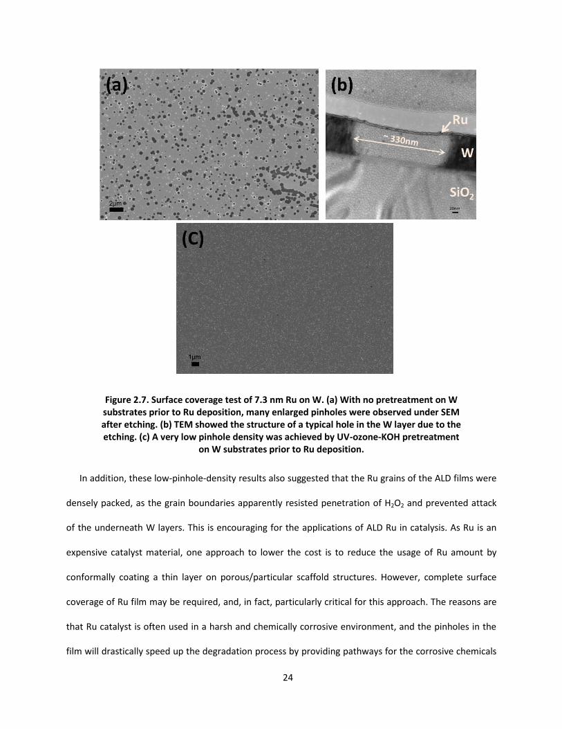
24
Figure 2.7. Surface coverage test of 7.3 nm Ru on W. (a) With no pretreatment on W substrates prior to Ru deposition, many enlarged pinholes were observed under SEM after etching. (b) TEM showed the structure of a typical hole in the W layer due to the etching. (c) A very low pinhole density was achieved by UV-ozone-KOH pretreatment
on W substrates prior to Ru deposition.
In addition, these low-pinhole-density results also suggested that the Ru grains of the ALD films were
densely packed, as the grain boundaries apparently resisted penetration of H2O2 and prevented attack
of the underneath W layers. This is encouraging for the applications of ALD Ru in catalysis. As Ru is an
expensive catalyst material, one approach to lower the cost is to reduce the usage of Ru amount by
conformally coating a thin layer on porous/particular scaffold structures. However, complete surface
coverage of Ru film may be required, and, in fact, particularly critical for this approach. The reasons are
that Ru catalyst is often used in a harsh and chemically corrosive environment, and the pinholes in the
film will drastically speed up the degradation process by providing pathways for the corrosive chemicals

25
to diffuse through and etch the underneath scaffold structure materials. Our surface pretreatment was
able to significantly reduce the pinhole density, but we have to admit that it seems difficult to achieve a
perfect 100% coverage without running the entire process in a cleanroom. On the bright side, the results
at least showed that the film quality will be good as long as a perfect nucleation layer is provided. In the
next section, we will discuss another approach to solve this problem, which is to in situ deposit two
layers without an air-break in between.
2.2.3 Summary
To sum up this section, we proceeded on the development of the ALD process of Ru with O2. A larger
O2 exposure window was achieved, which made this process less tricky to operate. Ru films grown on W
substrates were also investigated. No visible interfacial oxide layer was observed between Ru and W,
despite the fact that Ru films were deposited in an oxidizing ambient. The adhesion between Ru and W
was found to be very strong. An etching method was found to be effective for detecting small-size
pinholes in the Ru films. With the help of this technique, we found that nearly complete surface
coverage of Ru could be achieved by the correct surface pretreatments.
2.3 Pulsed Chemical Vapor Deposition of Ruthenium in a Reducing Ambient
In the previous section, we discussed an ALD process for Ru films from an amidinate precursor with
O2 as the co-reactant. Indeed, the Ru films had very good quality, but there were two major
disadvantages with that process. (1) Unwanted oxidation to conductive substrates is still a concern for a
process running in an oxidizing ambient. Even though we had proven that it was a fairly weak oxidizing
ambient, and the interfacial oxide layer, if there was any, did not cause any electrical problems under
optimal deposition conditions, we were still very interested in developing a process running in a
reducing ambient, so that the potential oxidation concern could be fundamentally circumvented. (2) As
ALD is known as a very slow process, a faster CVD process would be more promising for industrialization.

26
In this section, we discuss a pulsed CVD process of Ru from the same amidinate precursor (Figure 2.1),
but with NH3 and H2 gases as co-reactants. As it is a CVD process in a reducing ambient, it is considered
better for industrialization if it produces good quality of Ru films as well. Indeed, with this deposition
process, we were able to obtain low-resistance polycrystalline Ru films with bulk density, achieve good
adhesion to SiO2 substrates by introducing a thin layer of WN in between of the Ru and SiO2, and fully
cover the WN layer without any pinholes by only ~ 2 nm thick Ru films. Results of Ru film deposition
inside narrow holes also showed that good conformality was obtained by lowering the deposition
temperature. The surface of the deposited Ru films was fairly smooth, and the rms roughness value did
not increase significantly after rapid thermal annealing (RTA) at 700 °C.
2.3.1 Pulsed CVD Ru process and film characterization methods
Pulsed CVD of Ru was carried out in the same home-built tube reactor, with bis(N,N’-di-tert-
butylacetamidinato)ruthenium(II) dicarbonyl (Figure 2.1) as the Ru precursor and with NH3 and H2 gases
as co-reactants. The Ru precursor was placed in a glass bubbler in an oven at 140 °C or 150 °C, and it was
delivered by nitrogen carrier gas during each Ru pulse. NH3 gas flowed continuously at 2 Torr partial
pressure while the Ru precursor was delivered. After a fixed number of Ru precursor pulses, 3 Torr
hydrogen gas was supplied for one minute. The deposition procedure is schematically shown in Figure
2.8. We added these H2 steps because we found that they produced denser and more conductive Ru
films. We found that only supplying NH3 during deposition produced low-density Ru films, while only
supplying H2 did not even produce films, and if both NH3 and H2 were supplied simultaneously, the film
density was lower and the growth rate was also lower compared to the case of using only NH3. (See the
discussion of film density in Section 2.3.2 for more information.) The only way to achieve good film
quality was to add H2 steps in between two pulsed CVD cycles. Accordingly, we propose that the
mechanism of this deposition reaction consists of two steps: (1) NH3 reacts with the Ru precursor and
helps it stick on surface; and then (2) H2 helps remove the ligand and lower impurity level in film. We

27
would like to highlight this special process design, as it is de facto a hybrid process of pulsed CVD and
ALD. We believe that this special design will provide insights on making thin film materials that need
more than one co-reactant gas. If two co-reactant gases work synergistically in one reaction, those gases
can be supplied at the same time as a mixture gas, which is what people commonly use in CVD. However,
what if two gases need to do their own jobs separately, but work antagonistically when supplied
simultaneously? Our hybrid deposition procedure is designed to handle that case, as two gases are
separately provided during the deposition.
Figure 2.8. Schematic illustration of the pulsed CVD procedure with additional H2 intermediate steps.
Thermal SiO2 substrates were used for Ru deposition. They had 300 nm of thermal oxide on Si (100),
and were treated with UV/ozone for 5 minutes to remove surface organic contaminants before
deposition. Considering that Ru metal normally does not bond well to thermal oxide substrate due to
the relatively inert chemical property of thermal SiO2, an adhesion layer is necessary for those practical
applications that need some strength of adhesion. In our experiments, a thin layer of WN (typically 1 ~
10 nm) was introduced before Ru deposition in order to improve the adhesion. The deposition of WN
layers was carried out by ALD with bis(tert-butylimido)bis(dimethylamido)tungsten(VI) vapor and
ammonia gas. This WN ALD process was originally developed in our group,14 and some improvements

28
were developed as will be later discussed in Section 4.1. The as-deposited WN was amorphous, and its
surface is oxidized when exposed to air. In order to avoid oxidation of the WN, in situ Ru deposition was
followed right after the WN deposition in the same reactor without any air break.
The crystalline phase of deposited Ru films was evaluated by electron diffraction (ED) inside a
transmission electron microscope (TEM) (JEOL, Model JEL 2100). Film composition and number of atoms
per unit area were determined by Rutherford backscattering spectroscopy (RBS) and X-ray fluorescence
(XRF). Film thickness was measured by X-ray reflectometry (XRR) for relatively thick films (> 8nm), and
film density was calculated from the thickness and the number of atoms per unit area. For very thin
films, thickness cannot be directly measured by XRR. We assumed these films had the same density as
thick films that were deposited under the same conditions. Film chemical composition was also
evaluated by X-ray photoelectron spectroscopy (XPS) (ESCA, Model SSX-100). Film electrical sheet
resistance was measured by a four-point probe station (Veeco Instruments, Model FPP-100). Film
surface roughness was examined by atomic force microscopy (AFM) (Asylum, Model MFP-3D). The
adhesion energy of Ru/WN to SiO2 substrate was measured by four-point bend method. 11-13 Before the
measurement, samples were deposited with 0.13 μm of sputtered aluminum, and then attached by high
strength epoxy (EPO-TEK 353ND from Expoxy Technology) to a piece of dummy silicon water. The
bonded wafers were cut into 50 × 5 mm beams. Then, a notch was scribed at the center of each beam to
initiate a crack.
2.3.2 Properties of pulsed CVD Ru films
A 7 nm Ru film was deposited at 317 °C on a SiNx membrane TEM grid with 2 nm WN coating for
crystalline analysis. The TEM electron diffraction (ED) pattern (Figure 2.9) showed that all of the
observed rings belonged to the hexagonal Ru phase, which is also the stable phase of bulk Ru metal at
standard conditions. Another Ru film deposited on a planar substrate with the same deposition

29
conditions was examined by XPS for chemical composition analysis. The XPS spectrum (Figure 2.10)
showed that the Ru film was quite pure. Only Ru peaks were obviously observed in the spectrum, which
ruled out having nitrogen or oxygen incorporated in the film. (We could not draw conclusions on carbon,
since the C 1s peak overlaps with Ru 3d peaks.)
Figure 2.9. Electron diffraction pattern of a 7 nm Ru film on a SiNx membrane (50 nm) TEM grid with 2 nm amorphous WN deposited just before the Ru. The rings belong to hexagonal Ru phase, and the discrete spots came from Si substrate, which was used
for internal calibration.

30
Figure 2.10. XPS showing the Ru film was free of impurities. Notice that we could not draw conclusions on carbon since C 1s peak overlaps with Ru 3d peaks.
The film density was also evaluated with the atom areal density data measured by RBS or XRF, and
the thickness data measured by XRR. If only Ru/NH3 pulses were used, the film density was ~ 6 g/cm3, i.e.
only ~ 50% of the bulk value. Adding doses of hydrogen (H2) increased the film density up to the bulk
value. Films with bulk density were achieved if a hydrogen pulse was added after not more than about
0.1 nm of Ru growth. For example, in the case of depositing Ru at 317 °C, the growth rate was ~ 0.05
nm/pulse so a H2 pulse was added after every 2 Ru/NH3 pulses. This optimal condition was intuitively
reasonable, since 0.1 nm is about half the thickness of a monolayer, and the optimal condition
suggested that the rearrangement of surface Ru atoms was necessary before a monolayer of deposition
is completed. We tested Ru samples with different thicknesses (greater than 8 nm, so that reliable
thicknesses could be determined by XRR), and the density values were consistently around 12.13 g/cm3,
31
provided sufficiently frequent H2 doses were applied. These density values are very close to the bulk Ru
density value 12.18 g/cm3, which suggested that dense Ru films were obtained with our approach.
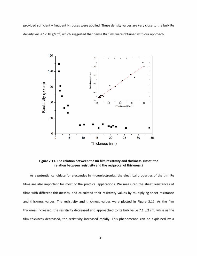
Figure 2.11. The relation between the Ru film resistivity and thickness. (Inset: the relation between resistivity and the reciprocal of thickness.)
As a potential candidate for electrodes in microelectronics, the electrical properties of the thin Ru
films are also important for most of the practical applications. We measured the sheet resistances of
films with different thicknesses, and calculated their resistivity values by multiplying sheet resistance
and thickness values. The resistivity and thickness values were plotted in Figure 2.11. As the film
thickness increased, the resistivity decreased and approached to its bulk value 7.1 μΩ cm; while as the
film thickness decreased, the resistivity increased rapidly. This phenomenon can be explained by a

32
scattering-induced-resistivity model, where the resistivity follows a linear relation with the reciprocal of
film thickness. The model can be expressed as 15
00 (1 )
t
t
,
where ρ is the thin film resistivity, ρ0 is the bulk resistivity taking into account the effect from impurity, t
is the film thickness, and t0 is a characteristic length, which is related to the electron mean free path and
scattering effects from grain boundaries, interfaces, surfaces and impurities. By plotting the resistivity
versus the reciprocal of thickness, and fitting with a linear model in the inset of Figure 2.11, we
extrapolated the film resistivity to a value ρ0 = 6.9 ± 1.9 μΩ cm, which is consistent with the bulk value of
pure Ru, 7.1 μΩ cm. The fitted t0 was 21 ± 6 nm.
Figure 2.12. AFM image of Ru/WN (~ 9nm/10nm) film on thermal SiO2 substrate. The rms roughness value is 0.28 nm.
The morphology of the film surface was also investigated. The AFM image (Figure 2.12) of a 9 nm
Ru film showed that the film surface was fairly smooth with an rms roughness value of 0.28 nm, or only
1.0
0.8
0.6
0.4
0.2
0.0
µm
1.00.80.60.40.20.0
µm
-400
-200
0
200
400
pm

33
3% of the film thickness. Since a small rms value does not guarantee that the film is pinhole-free, and
pinholes could cause problems in practice, we also examined pinholes by the etching method described
in Section 2.2.2. We used an etching solution that contained a mixture of H2O2, ammonia, and water
with a volumetric ratio of (30% H2O2):(concentrated NH3):H2O = 1:1:5. The etchant does not etch Ru
films, but when there are pinholes through a Ru film, the etchant can go through the pinholes and attack
the WN layer underneath. The place where the underlying WN is attacked by the etchant has a different
brightness under SEM. In order to have enough contrast under SEM, each of the samples here had a
relatively thick WN layer (~ 10 nm). Figure 2.13(a) shows a thin Ru film that did not fully cover the WN
layer, while Figure 2.13(b) shows that no pinholes were observed after a 10-minute etching of a thicker
Ru film. With this method, we were able to find the minimum thickness required for Ru to fully cover the
WN surface. Our results showed that many pinholes existed in a 1.3 nm Ru film (Figure 2.13(a)), but no
pinholes were observed in a 2.3nm Ru film (Figure 2.13(b)), which shows that only about 2 nm (~ 10
monolayers) of Ru is enough to fully cover the WN substrate. As compared with the coverage obtained
in Section 2.2.2, where ex situ prior-to-deposition surface cleaning was used, this in situ method
provided a much more effective way in avoiding the pinhole formation during the deposition.
Furthermore, the adhesion improvement by introducing a WN adhesion layer was confirmed by
four-point bend measurements. For a typical ~ 10 nm Ru film with thermal oxide as the substrate, 6.0
J/m2 of adhesion energy was observed with a 10 nm WN adhesion layer, comparing to only 0.8 J/m2
without the WN layer. Also, the delaminating interface was found at the WN/SiO2 interface, which
suggested that the adhesion energy between Ru and WN should be even greater than 6.0 J/m2. If
stronger adhesion is needed, one should focus on improving the strength of the WN/SiO2 interface.

34
Figure 2.13. SEM images of Ru/WN samples after 10-minute etching in H2O2/NH3, which dissolves WN but not Ru. The sample with (a) 1.3 nm Ru on 10 nm WN showed
many pinholes, while the sample with (b) 2.3 nm Ru on 10 nm WN did not have pinholes.
Step coverage is another important criterion for some applications of Ru films. One of the most
important potential applications is the electrode material in DRAM structures, where the metal needs to
be deposited inside hole structures.1 In order to obtain highly conformal deposition, lower deposition
temperature and higher precursor vapor pressure are usually needed.16 Therefore, we examined the
temperature dependence of the deposition rate as shown in Figure 2.14. The data (black filled squares)
suggested a typical CVD behavior. In the low temperature region (below 270 °C), the deposition rate was
limited by the surface reaction rate, and the logarithm of deposition rate followed a linear relation with
the reciprocal of temperature; at higher temperatures, the deposition rate drops below the linear curve
because diffusion starts to limit the growth rate. We also increased the precursor bubbler temperature
from 140 °C to 150 °C in order to get higher vapor pressure. A similar temperature dependence behavior
was obtained for deposition rate (green open squares in Figure 2.14), but with a higher deposition rate
above 270 °C. Below 270 °C, a higher bubbler temperature did not increase the deposition rate,

35
suggesting that the surface reaction rate had already reached saturation with vapor from the bubbler at
140 oC.
Figure 2.14. The relation of Ru deposition rate and deposition temperature. Black filled squares, and green open squares correspond to different bubbler temperatures,
i.e. 140 °C and 150 °C, respectively.
With the guidance of above observations, we deposited Ru inside narrow holes with an aspect ratio
(AR) of 40 (AR is defined as the ratio of depth to the diameter of each hole). The diameter and the depth
of each hole are 0.2 m and 8 μm, respectively. ~ 2 nm of WN was deposited before Ru deposition to
improve adhesion, since strong film-to-wall adhesion is preferred in practice for further fabrication steps,
such as chemical mechanical polishing (CMP). We chose to set 150 °C as the bubbler temperature, and
lowered the deposition temperature. We found that depositing at 317 °C did not give any film growth on
the bottom of the holes, but as we decreased deposition temperature, films became more and more

36
conformal. And eventually the film deposited at 242 °C gave fairly good conformality as shown in its
cross-sectional SEM image in Figure 2.15.
Figure 2.15. Cross-sectional SEM showing the conformality of Ru deposition. The holes are 0.2 μm in diameter and 8 μm in depth (aspect ratio is 40:1). 2 nm of highly
conformal WN was deposited first, and then followed with Ru deposition at 242°C. Values in parentheses are the film thicknesses at corresponding depths along the hole.
There are also some applications where Ru films have to experience a high temperature annealing
process.1 During the annealing process, agglomeration could roughen the surface of the films. Therefore,
we also measured the surface roughness of a Ru/WN film before and after rapid thermal annealing

37
(RTA). The thicknesses of Ru and WN layers were 13 nm, and 3 nm, respectively, and the RTA was
performed at 700 °C for 2 min. The surface morphology was examined by AFM (Figure 2.16), showing
that the rms roughness value increased from 0.5 nm to 1.4 nm after RTA. Considering that the rms value
after annealing was still much smaller than the film thickness, a slight increase in surface roughness may
be acceptable for practical applications.
Figure 2.16. AFM images of Ru/WN (13nm/3nm) film on thermal SiO2 substrate. The rms roughness values for (a) as-deposited film, and (b) 2 min 700 °C RTA film were 0.5
nm, and 1.4 nm, respectively.
2.3.3 Conclusions
With our newly developed pulsed CVD process, we were able to grow Ru thin films with bulk
density, low resistivity, and smooth surface morphology. Depositing a thin layer of WN before Ru
deposition greatly increased the adhesion of the Ru film to SiO2 substrate. Only ~ 2 nm of Ru film was
needed to fully cover the WN layer without any pinholes. Deposition of Ru inside narrow holes was also
investigated. Fairly good conformality was obtained by lowering the deposition temperature. Film
roughness did not increase too much after 700 °C RTA. The properties we obtained above would satisfy
many requirements for potential applications of Ru thin films. As it is a CVD process in a reducing
ambient, we believe it is promising for industrialization.

38
2.4 References
1 S. K. Kim, S. W. Lee, J. H. Han, B. Lee, S. Han, and C. S. Hwang, Adv. Funct. Mater. 20, 2989 (2010).
2 S. K. Kim, G. J. Choi, S. Y. Lee, M. Seo, S. W. Lee, J. H. Han, H. S. Ahn, S. Han, and C. S. Hwang,
Advanced Materials 20, 1429 (2008).
3 V. Misra, G. Lucovsky, and G. N. Parsons, MRS Bull. 27, 212 (2002).
4 O. K. Kwon, J. H. Kim, H. S. Park, and S. W. Kang, J. Electrochem. Soc. 151, G109 (2004).
5 A. Ozaki, Accounts Chem. Res. 14, 16 (1981).
6 T. Aaltonen, P. Alen, M. Ritala, and M. Leskela, Chem. Vapor Depos. 9, 45 (2003).
7 T. Aaltonen, M. Ritala, K. Arstila, J. Keinonen, and M. Leskela, Chem. Vapor Depos. 10, 215
(2004).
8 B. S. Kang, et al., Appl. Phys. Lett. 91 (2007).
9 H. Z. Li, T. Aaltonen, Z. W. Li, B. S. Lim, and R. G. Gordon, Open Inorg. Chem. J. 2, 11 (2008).
10 H. T. Wang, R. G. Gordon, R. Alvis, and R. M. Ulfig, Chem. Vapor Depos. 15, 312 (2009).
11 R. Dauskardt, M. Lane, Q. Ma, and N. Krishna, Eng. Fract. Mech. 61, 141 (1998).
12 M. Lane, R. H. Dauskardt, A. Vainchtein, and H. J. Gao, J. Mater. Res. 15, 2758 (2000).
13 Y. Lin, J. J. Vlassak, T. Y. Tsui, and A. J. Mckerrow, Mat. Res. Soc. Symp. Proc. 795, 93 (2004).
14 J. S. Becker, S. Suh, S. L. Wang, and R. G. Gordon, Chem. Mat. 15, 2969 (2003).
15 S. M. Rossnagel and T. S. Kuan, J. Vac. Sci. Technol. B 22, 240 (2004).
16 A. Yanguas-Gil, Y. Yang, N. Kumar, and J. R. Abelson, Journal of Vacuum Science & Technology A
27, 1235 (2009).

39
Chapter 3 Pulsed Chemical Vapor Deposition of
Ruthenium Dioxide and Epitaxy Analysis
3.1 Pulsed CVD of RuO2
Ruthenium dioxide (RuO2) has many unique properties. RuO2 has metallic conductivity at room
temperature and good thermal stability, which make it suitable as an electrode material for field
emission cathodes1 and dynamic random access memory (DRAM).2 Due to its good redox properties,
RuO2 has been made into electrodes for supercapacitors.3-5 The high work function of RuO2 makes these
capacitors have low leakage current. Also, RuO2 has a relatively small magneto-resistance, and therefore
it has been used in cryogenic temperature sensors.6, 7 Moreover, RuO2 has been extensively studied as a
catalyst for oxidation of CO8-10 and HCl,11 as well as an electrocatalyst of chlorine evolution12, 13 and
oxygen evolution14 in electrolysis. In industry, RuO2 is the main active component in dimensionally stable
anodes (DSA®) in chlorine production.15
Our RuO2 films were made from the same amidinate Ru precursor as used in Chapter 2 for depositing
Ru metal films, i.e. bis(N,N’-di-tert-butylacetamidinato)ruthenium(II) dicarbonyl (Figure 2.1). But for
depositing RuO2 films, the deposition was run in pulsed CVD conditions with O2 gas as the co-reactant.
The Ru precursor was placed in a glass bubbler in an oven at 140 °C, and it was delivered into the reactor
tube with nitrogen carrier gas in each precursor pulse. At a deposition temperature of 280 °C, the
exposure of Ru precursor was estimated to be 7.5 mTorr s for each pulse. A gas mixture of oxygen and
nitrogen (O2:N2 = 1:2 in partial pressure) was kept flowing at a total pressure of 0.45 Torr, while the Ru
precursor was delivered. We found it was important to keep enough O2 present in the ambient when
the Ru precursor was introduced into the chamber, since, otherwise, Ru metal films, instead of RuO2,
would be formed, as shown in Section 2.2. The minimum O2 partial pressure required for depositing

40
RuO2 has not been tested, but with the lowest O2 partial pressure we tried, i.e. 0.05 Torr (O2:N2 = 1:8),
we were still able to obtain RuO2 films with the same structural and electrical properties. Thermal SiO2
substrates were used as substrates. Each substrate was treated with UV/ozone for 5 minutes to remove
surface organic contaminants before deposition.
At a typical deposition temperature of 280 °C, the growth rate was measured to be 0.092 nm per
pulse. As for a typical CVD reaction, the film thickness usually decreases from the inlet to the outlet due
to the depletion of the precursor vapor as it converts into solid film when it travels along the tube. For
this pulsed CVD Ru process at 280 °C, the decrease in film thickness was found to be only 10% for the
first 6 inches from the inlet. Lowering the deposition temperature to 250 °C, further improved
uniformity down to <5% decrease, but the growth rate also decreased to 0.046 nm per pulse, while the
structural and electrical properties of the films remained the same. On the other hand, elevating the
deposition temperature to 310 °C was also investigated. Even though we could clearly observe an
increase in growth rate, we also observed greater non-uniformity of film thickness and color across the
sample holder in the direction perpendicular to the gas flow. This is because the vapor was also
depleted by the deposition on the tube wall, and consequently, the film was thicker in the center half-
inch stripe parallel to the gas flow, but thinner in the outer two stripes closer to the wall. Considering
the above results, we decided to choose 280 °C as our deposition temperature for further studies, as it
produces RuO2 films with good uniformity, reasonable growth rate, and good film quality as will be
shown in the following.
The crystallinity of a 46 nm RuO2 film deposited on a thermal oxide substrate was examined by X-ray
diffraction (XRD). All the peaks observed in the θ-2θ scan (Figure 3.1) matched well with the database
values of rutile RuO2 (PDF 00-040-1290). Furthermore, TEM studies of a 6 nm RuO2 film deposited on a
50 nm SiNx membrane TEM grid showed that the crystal size was around 8 nm, and the corresponding
electron diffraction pattern confirmed that only rutile RuO2 diffraction rings were shown (Figure 3.2).

41
Figure 3.1. XRD of a 46 nm RuO2 film. All the peaks belong to rutile RuO2.
Figure 3.2. (a) TEM image of a 6 nm RuO2 film deposited on a SiNx membrane (50 nm) TEM grid, and (b) the electron diffraction pattern showed rings only belong to rutile RuO2, while the Si substrate produced discrete spots, which were used for internal
calibration.
35 40 45 50 55
0
20
40
60
80
100
120
(111)
(211)(200)
Inte
nsity
2 ()
(101)

42
The film density was evaluated with the atom areal density data measured by RBS, and the thickness
data measured by XRR. For a 35 nm RuO2 film, the density was determined to be 7.02 g/cm3, which is
equal to the RuO2 bulk density. The resistivity was measured to be 130 μΩ cm, which is about 3 times
higher than its bulk value (~ 40 μΩ cm). This is likely due to the strong electron scattering effect caused
by small RuO2 grain size. The surface morphology was examined by AFM, showing that the rms
roughness was only 0.35 nm for a 36 nm film.
Figure 3.3. AFM images of a 36 nm RuO2 film grown on thermal SiO2 substrate. The rms roughness was 0.35 nm.
3.2 High quality epitaxy of RuO2 on TiO2 (011)
3.2.1 Introduction
RuO2 has the rutile structure with lattice constants very similar to rutile TiO2. Rutile TiO2 has a high
dielectric constant, and therefore, a capacitor with high capacitance per unit area can be made by a
stack structure of RuO2/TiO2/RuO2.16 In this structure, RuO2 substrates induce TiO2 to grow epitaxially in
its rutile form with high dielectric constant, rather than in its anatase form with lower dielectric constant.
Ultrathin RuO2 supported on TiO2 rutile forms an efficient and stable catalyst for gas-phase oxidation of
1.0
0.8
0.6
0.4
0.2
0.0
µm
1.00.80.60.40.20.0
µm
-800
-600
-400
-200
0
200
400
600
800
pm

43
HCl, which has implemented for large-scale production of chlorine.17 Several studies have followed to
investigate the mechanism of this RuO2/TiO2 catalyst.18, 19
Transition metal oxides are usually grown by pulsed laser deposition (PLD), molecular beam epitaxy
(MBE), magnetron sputtering (MS), and chemical vapor deposition (CVD).20 Among these techniques,
CVD has been used to grown many different kinds of oxide films, including ferromagnetic CrO2,20 wide-
gap semiconductors ZnO20, 21 and SnO2,22, 23 superconducting oxides,24 and oxide gate electrode
materials.25 Compared with other techniques, CVD can often be done at a fairly low temperature in a
low vacuum level chamber or at atmospheric pressure.26 Therefore, it has advantages in making
thermally or in vacuo unstable epitaxial films.20 The RuO2/TiO2 interface has been reported unstable at
high temperature, as RuO2 and TiO2 begin to interdiffuse to form a Ti(1-x)RuxO2 alloy above 400 °C on (110)
surface.27, 28 Moreover, the (011) surface of TiO2 is even thermodynamically less stable than the (110), as
the (011) surface reconstructs at 800 °C.29
In order to study the structure of RuO2 on TiO2, we grew RuO2 thin films on single-crystal TiO2
substrates using the pulsed CVD process, as mentioned previously, at 280 °C substrate temperature. At
this low temperature, little or no interdiffusion occurs, so the RuO2 film remains pure. We chose to grow
RuO2 on rutile TiO2 (011) surfaces, since the (011) plane gives relatively small lattice mismatches of - 2.0%
along the [100] direction, and + 0.07% along the ]101[ direction. The resulting RuO2/TiO2 structures
were studied by reciprocal space mapping by high-resolution X-ray diffraction (HRXRD). Our results show
that a high quality epitaxial RuO2 film was grown on the TiO2 (011) substrate (supplied by MTI
Corporation). The thin RuO2 film is constrained to match the lattice constants of the TiO2 substrate in
the two planar directions. However, the RuO2 is partially relaxed in the direction perpendicular to the
substrate, resulting in a slight monoclinic distortion of the film. This result is the first complete HRXRD
analysis of a non-cubic epitaxial film.

44
3.2.2 Epitaxy analysis by HRXRD
Due to the close lattice structures of RuO2 and TiO2, the crystal structure of epitaxial RuO2 film was
examined by high-resolution X-ray diffraction (HRXRD). We employed HRXRD for reciprocal space
mapping of the reciprocal lattice profile of a sample with RuO2 film grown on TiO2 (011) substrate.
Reciprocal space mapping is a useful approach to examine the structure and the quality of epitaxy. By
using the reciprocal lattice of the substrate TiO2 as the internal reference, and examining the fine
structure of representative reciprocal lattice points, we would be able to reconstruct the reciprocal
lattice profile of RuO2, and therefore understand the distortion of the RuO2 lattice, as well as the relative
lattice alignment of the RuO2 film and the TiO2 substrate. However, unlike film grown on (100) of a cubic
structure substrate (e.g. Si, Ge, and GaAs), the RuO2 was grown on (011) of tetragonal TiO2, which has a
lower symmetry. The distortion of RuO2 can be different in two orthogonal lateral directions. Therefore,
we should choose representative reciprocal lattice points in both orthogonal lateral directions.
The HRXRD instrument we used was Bruker D8 HRXRD. The incident beam for HRXRD (Cu Kα1) was
monochromated by a Ge (022) × 4 asymmetric monochromator, and a scintillation point detector
(Pathfinder) with a Ge (022) × 3 analyzer inserted was used to collect the X-ray signal.
The sample was first aligned in the (φ = 0°) configuration where TiO2 [100] was coplanar with the
incident and exit X-ray beams, as shown in Figure 3.4(a). We chose to perform the out-of-plane
reciprocal space mappings (scanning ω and 2θ) of (011) and (222) reflections. (The (111) reflection is not
allowed in the Bragg reflection geometry with this configuration.) Then, we rotated the sample by ± 90°,
so that we could perform the out-of-plane reciprocal space mappings in the orthogonal plane (not
shown in Figure 3.4(a)). In this configuration (φ = ± 90°), we chose the (011), (031), and (013) reflections,
since many other low miller index planes are not allowed in the Bragg reflection geometry.

45
Figure 3.4. (a) Experimental configuration of HRXRD. (b) Schematic illustration of reciprocal space mappings.
Notice that, unlike a cubic structure, for a tetragonal structure, [011] is not the normal direction of
the (011) plane, therefore, in order to avoid confusion, we will discuss our results mainly in the
reciprocal space, since the reciprocal space mapping technique gives direct information in reciprocal
space. We further define the coordinates in reciprocal space in the substrate reference frame as follows:
x is the direction of [100], z is the normal direction of the (011) plane, and y is the direction of z × x
(Figure 3.4(b)). Therefore, the previously mentioned measurements correspond to the (qx,qz) area
mappings of the (011) and (222) reflections in x-z plane (φ = 0° configuration), and the (qy,qz) area
mappings of the (011), (031), and (013) reflections in y-z plane (φ = ± 90° configuration), respectively.
With the fine reciprocal space structure of two orthogonal planes, we expected to construct the whole
three-dimensional reciprocal lattice profile.
The reciprocal space maps of the symmetric (011) reflection are shown in Figure 3.5(a, b). Two maps
correspond to two perpendicular projections of the three-dimensional lattice profile in reciprocal space
on x-z and y-z planes, respectively. The intensity contours are shown on logarithmic scale. Along with
the TiO2 (011) peak, both the RuO2 (011) main peak and its thickness fringes (denoted as “F” in Figure
3.5) were clearly observed, which suggested that it was a high quality epitaxial growth of RuO2 on TiO2
RuO2
TiO2
(011) Plane[100]
2θω
φ
X Ray Detector
RuO2
TiO2
(011) Plane[100]
2θω
φ
X Ray Detector
x-z plane
x
yz
y-z pla
ne
(222)
(011)
(031)
(013)
[100]
[010][001]
x-z plane
x
yz
y-z pla
nex-z plane
x
yz
y-z pla
ne
(222)
(011)
(031)
(013)
[100]
[010][001]

46
(011). Using the TiO2 (011) peak as the internal reference, the 2θ value of RuO2 (011) main peak was
35.5421°. Comparing with the reference value of 35.0505° (PDF 00-040-1290) measured from a bulk
crystal, we found that the peak position shifted by ~ 0.49° due to the distortion imposed by the TiO2
substrate. There were also a few detailed features we noticed in these two reciprocal space maps. First,
the TiO2 substrate was not a perfect single crystal; it had several mosaic blocks as shown as satellite
peaks in the Δω-axis direction (denoted as “M” in Figure 3.5), which corresponds to sample rocking (Δω
is the sample tilting angle). And, interestingly, the RuO2 peaks also showed correlated satellite peak
shapes in the Δω-axis direction, which suggested that our RuO2 film was epitaxially grown on each
individual block of TiO2. Besides, the spreading of the RuO2 (011) main peak in Δω-axis direction was
very close to that of the substrate peak, which again suggested a high quality of epitaxy. We further
noticed that, in Figure 3.5(a), the RuO2 peaks were not exactly located on the Δω = 0 line. This was due
to a small miscut of our TiO2 substrate. Since the direction defined by the film main peak and thickness
fringes is the physical surface normal direction, and the Δω = 0 line corresponds to the normal direction
of the crystal lattice plane, the angle between these two directions corresponds to the miscut angle of
the substrate, which was calculated to be ~ 0.3°. Furthermore, the TiO2 (011) peak was collinear with
RuO2 (011) main peak and its fringes, which provided the information regarding the growth direction of
the RuO2 film. We will come back to discuss this later in this paper. Nevertheless, we will neglect this
small miscut angle for now, and the error of neglecting will be discussed later. In addition, the thickness
of the RuO2 film can be extracted from the periodicity of the thickness fringes. In order to have a better
fitting, we performed a coupled ω-2θ scan with smaller step size and longer collecting time with φ = 90°
configuration. The data are plotted in Figure 3.5(c), and the film thickness was determined to be ~ 38 nm.

47
Figure 3.5. Reciprocal space maps of the (011) reflection in (a) x-z plane and (b) y-z plane. “F” and “M” denote the satellite peaks due to thickness fringes and mosaic blocks, respectively. (c) Coupled ω -2θ scan of the (011) reflection. The (011) peak
position for bulk RuO2 is also shown for comparison.
Then, we performed the reciprocal space mappings of the asymmetric (222), (031), and (013)
reflections to obtain the reciprocal lattice profile in both x-z and y-z planes, which would lead us to
understand the full lattice structure of the RuO2 film grown on TiO2 (011). The (qx,qz) area mapping of
the (222) reflection is shown in Figure 3.6, and the (qy,qz) area mappings of the (031), and (013)
reflections are shown in Figure 3.7 and Figure 3.8, respectively. The peak position of the RuO2 (222)
reflection was observed at Δω = - 0.3562° and 2θ = 88.2871° in Figure 3.6, the peak position of RuO2
(031) reflection was observed at Δω = 0.6271° and 2θ = 70.5549° in Figure 3.7, and the peak position of
34.8 35 35.2 35.4 35.6 35.8 36 36.2 36.4
-0.1
-0.08
-0.06
-0.04
-0.02
0
0.02
0.04
0.06
0.08
0.1(a)
Δω
(°)
2θ (°)
TiO2
(011)
RuO2
(011)
M
FF
FF
M
M
Surface
normal
34.8 35 35.2 35.4 35.6 35.8 36 36.2 36.4
-0.1
-0.08
-0.06
-0.04
-0.02
0
0.02
0.04
0.06
0.08
0.1(a)
Δω
(°)
2θ (°)
TiO2
(011)
RuO2
(011)
M
FF
FF
M
M
Surface
normal
34.8 35 35.2 35.4 35.6 35.8 36 36.2 36.4
-0.1
-0.08
-0.06
-0.04
-0.02
0
0.02
0.04
0.06
0.08
0.1(b)
Δω
(°)
2θ (°)
TiO2
(011)
RuO2
(011)
FF FF
M
34.8 35 35.2 35.4 35.6 35.8 36 36.2 36.4
-0.1
-0.08
-0.06
-0.04
-0.02
0
0.02
0.04
0.06
0.08
0.1(b)
Δω
(°)
2θ (°)
TiO2
(011)
RuO2
(011)
FF FF
M
34.5 35.0 35.5 36.0 36.5
100
101
102
103
104
105
106
Inte
nsity
2
(c)
Inte
nsi
ty
2θ (°)
TiO2 (011)
RuO2 (011)
RuO2 (011)
Bulk
34.5 35.0 35.5 36.0 36.5
100
101
102
103
104
105
106
Inte
nsity
2
(c)
Inte
nsi
ty
2θ (°)
TiO2 (011)
RuO2 (011)
RuO2 (011)
Bulk

48
RuO2 (013) reflection was observed at Δω = - 0.8080° and 2θ = 100.7082° in Figure 3.8. In these three
figures, similar fine features of the contour shape are observed as in Figure 3.5: satellite peaks in the
Δω-axis direction, which correspond to the mosaic blocks of the substrate TiO2; similar widths of the
peak spreadings in the Δω-axis direction for both the substrate and the film main peaks; clear thickness
fringes and the collinearity of the film main peak, thickness fringes, and the substrate main peak. All of
these observations again indicated a high quality epitaxy of RuO2 grown on TiO2 (011).
Figure 3.6. Reciprocal space map of the (222) reflection in x-z plane. “F” and “M” denote the satellite peaks due to thickness fringes and mosaic blocks, respectively.
Figure 3.7. Reciprocal space map of the (031) reflection in y-z plane. “F” denotes the satellite peaks due to thickness fringes.
87.5 88 88.5 89 89.5 90-0.6
-0.5
-0.4
-0.3
-0.2
-0.1
0
0.1
0.2
Δω
(°)
2θ (°)
TiO2
(222)
RuO2
(222)
F
F
F
F
M
87.5 88 88.5 89 89.5 90-0.6
-0.5
-0.4
-0.3
-0.2
-0.1
0
0.1
0.2
Δω
(°)
2θ (°)
TiO2
(222)
RuO2
(222)
F
F
F
F
M
69 69.5 70 70.5 71
-0.2
0
0.2
0.4
0.6
0.8
Δω
(°)
2θ (°)
TiO2
(031)
RuO2
(031)
F
F
F
FF
69 69.5 70 70.5 71
-0.2
0
0.2
0.4
0.6
0.8
Δω
(°)
2θ (°)
TiO2
(031)
RuO2
(031)
F
F
F
FF

49
Figure 3.8. Reciprocal space maps of the (013) reflections of (a) the TiO2 substrate and (b) the RuO2 film in y-z plane. “F” and “M” denote the satellite peaks due to thickness fringes and mosaic blocks, respectively. Notice that (a) and (b) are on different scales.
In combination with the peak positions of the RuO2 (011), (222), (031), and (013) reflections, we were
able to construct the reciprocal lattice structure of the RuO2 film with respect to that of the TiO2
substrate. Reciprocal lattice patterns in the x-z and y-z planes are shown in Figure 3.9(a) and (b),
respectively. As the patterns indicated, the RuO2 lattice was fully pinned by the substrate laterally: each
of the film reciprocal lattice point was right below its corresponding substrate reciprocal lattice point.
Only the direction normal to the surface had some degree of relaxation. Moreover, we found the angle
between the (010) and (001) reflections was 89.23°, which is slightly distorted from a right angle. Thus
the RuO2 film lost its tetragonal symmetry and became a monoclinic structure, although the difference is
not large. In addition, since the film main peak and its thickness fringes determine the normal direction
of the surface, this fully pinned structure was also consistent with the collinearity we observed in Figures
2 – 5. Finally, the RuO2 film grown on TiO2 (011) had a monoclinic structure, with lattice parameters of a
= 4.5933 Å, b = 4.4647 Å, c = 3.0889 Å, and α = 89.23°. Notice that the lattice constant a of RuO2 was
stretched to be equal to that of TiO2, due the lateral pinning effect imposed by the substrate.
105.9 105.95 106 106.05 106.1 106.15
-0.06
-0.04
-0.02
0
0.02
0.04
0.06
Δω
(°)
2θ (°)
(a)
M
TiO2 (013)
M
105.9 105.95 106 106.05 106.1 106.15
-0.06
-0.04
-0.02
0
0.02
0.04
0.06
Δω
(°)
2θ (°)
(a)
105.9 105.95 106 106.05 106.1 106.15
-0.06
-0.04
-0.02
0
0.02
0.04
0.06
Δω
(°)
2θ (°)
105.9 105.95 106 106.05 106.1 106.15
-0.06
-0.04
-0.02
0
0.02
0.04
0.06
Δω
(°)
2θ (°)
(a)
M
TiO2 (013)
M
100 100.2 100.4 100.6 100.8 101 101.2
-0.9
-0.85
-0.8
-0.75
-0.7
Δω
(°)
2θ (°)
(b)
FF
RuO2 (013)
100 100.2 100.4 100.6 100.8 101 101.2
-0.9
-0.85
-0.8
-0.75
-0.7
Δω
(°)
2θ (°)
(b)
FF
RuO2 (013)

50
Figure 3.9. Reciprocal lattice profile of the RuO2 film (red dots) and the TiO2 substrate (black dots) (a) in x-z plane, and (b) in y-z plane For comparison, the unstrained (bulk)
RuO2 reciprocal lattice was also plotted (open blue circles).
0 1 2 3
0
1
2
3
4
5
(000)
(011)
(022)
(100)
(111)
(122) (222)
(211)
(200)
(a)
qx (Å-1)
qz
(Å-1
)
0 1 2 3
0
1
2
3
4
5
(000)
(011)
(022)
(100)
(111)
(122) (222)
(211)
(200)
(a)
qx (Å-1)
qz
(Å-1
)
-3 -2 -1 0 1 2 3
0
1
2
3
4
5
6
7
(000)
(011)
(022)
(010)
(001) (020)
(031)
(021)
(012)
(002)
(013)
qy (Å-1)
qz
(Å-1
)
(b)
-1.16 -1.15 -1.141.6
1.7
1.8
qy (Å-1)
qz
(Å-1
)
1.14 1.15 1.16
0.7
0.8
0.9
qy (Å-1)
qz
(Å-1)
-3 -2 -1 0 1 2 3
0
1
2
3
4
5
6
7
(000)
(011)
(022)
(010)
(001) (020)
(031)
(021)
(012)
(002)
(013)
qy (Å-1)
qz
(Å-1
)
-3 -2 -1 0 1 2 3
0
1
2
3
4
5
6
7
(000)
(011)
(022)
(010)
(001) (020)
(031)
(021)
(012)
(002)
(013)
qy (Å-1)
qz
(Å-1
)
(b)
-1.16 -1.15 -1.141.6
1.7
1.8
qy (Å-1)
qz
(Å-1
)
-1.16 -1.15 -1.141.6
1.7
1.8
qy (Å-1)
qz
(Å-1
)
1.14 1.15 1.16
0.7
0.8
0.9
qy (Å-1)
qz
(Å-1)
1.14 1.15 1.16
0.7
0.8
0.9
qy (Å-1)
qz
(Å-1)

51
Figure 3.10.Blow up of the reciprocal lattice profile near (a) (011) and (b) (222) in the x-z plane. (c) Schematically illustration of the effect of miscut.
Now we would like to discuss the effect of the small miscut as mentioned previously. First of all, we
will only discuss the effect of the miscut in [100] direction, which corresponded to the reciprocal space
mapping of the x-z plane (Figure 3.5(a)), since in the y-z plane, the miscut effect was almost
unobservable as shown in Figure 3.5(b). Noticing that the film was fully pinned by the substrate, the
effect of the small miscut we observed led to a small rotation of the RuO2 reciprocal space profile with
respect to the substrate profile. As a result, the RuO2 (011) reciprocal lattice point shifted laterally as
shown in Figure 3.10. For this sample, the shift was 0.0002 Å-1 based on our reciprocal space mapping
data of the (011) reflection. And this corresponded to a 0.0046° of rotation of the RuO2 lattice in the
reciprocal space. Then, we used this rotation value to predict the lateral shift of the RuO2 (222), which
was calculated to be 0.0004 Å-1. This value was exactly the same as we extracted from our experimental
data of the reciprocal space map of the (222) reflection. Indeed the effect of the miscut was observable
by our measurements, the effect of this small miscut was very small, and its influence on the peak
positions of the RuO2 (031) and (013) reflections was also negligible. Nevertheless, this miscut caused
the rotation in reciprocal space. However, we propose that if the RuO2 film is grown on a zero-miscut
TiO2 (011) substrate, there will be no rotation in reciprocal space; each pair of the reciprocal lattice
points of the RuO2 and TiO2 will be perfectly aligned in the normal direction of the surface.

52
3.2.3 Other measurements
The above HRXRD results clearly indicated that the RuO2 grown on TiO2 was a high quality epitaxy
with a laterally fully pinned structure. In particular, the clear thickness fringes suggested a smooth
surface and a low level of defects of the RuO2 film. We further examined the surface roughness by AFM
(Asylum, Model MFP-3D), and the interface of RuO2 and TiO2 by cross-sectional TEM (JOEL 2100).
The AFM (Figure 3.11) results confirmed the smoothness of the film, with an rms roughness value of
only 0.78 nm for a 40 nm film. And the TEM image (Figure 3.12) showed a perfect alignment of the RuO2
and TiO2 lattices. Also no interfacial layer was observed. These good properties can be attributed to the
low temperature pulsed CVD process. At the process temperature of 280 °C, the interdiffusion rates of
Ru and Ti atoms are very slow, while the surface mobility of Ru atoms is still high; probably, with the
help from ligand and/or co-reactant oxygen.
Figure 3.11. AFM image of the RuO2 film surface.
1.0
0.8
0.6
0.4
0.2
0.0
µm
1.00.80.60.40.20.0
µm
-1.0
-0.5
0.0
0.5
1.0nm

53
Figure 3.12. Cross-sectional TEM of RuO2/TiO2 interface.
3.2.4 Conclusions
In this work, we presented a low temperature pulsed CVD process to grow epitaxial RuO2 thin film on
TiO2 (011) substrate. The epitaxial structure was examined by HRXRD. We collected the reciprocal space
maps of the (011), (222), (031), and (013) reflections. The clear thickness fringes and small spreading of
the film peaks both suggested high quality of the epitaxy. Based on the reflection peak positions of the
RuO2 and TiO2, we were able to construct the reciprocal lattice profile of RuO2. The results showed that
the RuO2 film was fully pinned by the substrate in both lateral directions, but distorted in the direction
perpendicular to the surface of the substrate.

54
3.3 RuO2 bottom electrode for studying metal-insulator transition characteristics of
VO2
3.3.1 Introduction
Vanadium dioxide (VO2) shows a metal-insulator transition (MIT) with several orders of magnitude
conductivity change, accompanied by a phase change from high temperature tetragonal rutile structure
(P42/mnm) to low temperature monoclinic structure (P21/c).30 The phase change is accomplished by a
small lattice distortion along the c axis of the tetragonal structure hence forming V-V pairs along a axis in
the monoclinic structure. The transition temperature could be manipulated to either higher or lower
temperature through cation substitution as investigated early in late 60’s, for example: W6+, Nb5+, Ru4+,
etc. Doping of most higher valence state (≥ 4+ except Ge4+) cations depresses the transition temperature,
while M3+ ( M = Cr, Fe, Ga, and Al) doping elevates the transition temperature.31
It is important to deposit high quality VO2 films on conductive substrates for studying the carrier
transport in the out-of-plane direction of the films. Most of the studies in this regard focused on the VO2
films grown on heavily-doped Si or Ge, and Pt substrates.32-34 However, it would be of particular interest
to investigate the VO2 films grown on conductive oxide substrates, since the oxide underlayer also works
as an electrode in all-oxide electronics. Recently, there is a published report investigating the VO2 films
grown on conductive Ga-doped ZnO coated c-sapphire substrates, in which the twin boundaries of
VO2/ZnO were found important for carrier transport.35 In this study, we use conductive RuO2 as the
bottom electrode material. We investigate the physical properties of the VO2 films grown on conductive
RuO2 films which are epitaxially grown on TiO2 single crystal substrates. And the VO2 films grown on
commercially available conductive oxide substrates, Nb-doped SrTiO3 single crystal substrates, are also
investigated for comparison.

55
VO2 films were deposited by Dr. Yanjie Cui in Prof. Ramanathan’s group at Harvard University. The
VO2 thin films (~ 200nm) were deposited by RF-sputtering on two types of conductive oxide substrates:
Nb-doped SrTiO3 (001) (Nb:STO) and RuO2 (101) buffered TiO2 (101) single crystal substrates (RuO2/TiO2).
The single crystals of Nb:STO (Nb weight concentration 1.0%) with a resistivity of 3.5 mΩ cm were used
as-obtained (from MTI Crystal) except for high pressure nitrogen blowing before loading into a
sputtering chamber. Crystalline RuO2 thin films were grown by pulsed chemical vapor deposition (pulsed
CVD) in a home-built tube reactor, with bis(N,N’-di-tert-butylacetamidinato)ruthenium(II) dicarbonyl as
the ruthenium precursor and oxygen as co-reactant gas, at a deposition temperature of 280 °C. Details
of the deposition process can be found in Section 3.1. Rutile TiO2 (101) substrates supplied by MTI
Corporation were used for growing epitaxial RuO2 films. The RuO2 film thickness is ~ 38 nm with
resistivity of 80 μΩ cm. The sputtering process of VO2 was performed in an argon environment at a set
pressure of 10 mTorr. V2O5 was used as the target material. The substrate temperature and RF source
power were set at 550 oC and 120 W, respectively. Details of the sputtering process can be found in
other reports.33, 36 Au (200 nm) / Ti (20 nm) metal contacts with sizes ranging from 50×50 m2 to
500×500 m2 were deposited in a Denton E-Beam Evaporator with a shadow mask.
3.3.2 Structural analysis of VO2 on Nb:STO and RuO2/TiO2
Figure 3.13 shows the 2- coupled X-ray diffraction patterns for the VO2 films grown on a Nb:STO
single crystal substrate and a RuO2 buffered TiO2 single crystal substrate, respectively. The VO2 film on
Nb:STO is highly textured, as shown in Figure 3.13(a): the major peaks at 2θ = 27.83o and 57.44o belong
to the (011) and (022) reflections of the monoclinic phase of VO2, respectively, and all the other minor
peaks can be assigned to VO2 or the substrate Nb:STO. For the VO2 film grown on RuO2, we performed a
high-resolution XRD scan as shown in Figure 3.13(b). The peaks at 35.77o, 36.11o, 37.13o, are ascribed to
the (101) reflections of the tetragonal RuO2, TiO2 and VO2, respectively. As shown previously (Figure 3.5),
the RuO2 (101) peak shifts from 35.05o (as for a bulk single crystal) to 35.54o (when epitaxially grown on

56
a rutile TiO2 (101) substrate) due to the lattice strain induced by the substrate (the (101) peak of single
crystal rutile TiO2 is at 36.08 o). The TiO2 substrate forces the RuO2 lattice to expand to match the basal
size in the lateral direction, while decreasing the d101 spacing of the RuO2 lattice. (The related
crystallographic information is listed in Table 3.137-40). After growing VO2 on top, the RuO2 (101) peak
further shifted to an even higher angle of 35.77 o. (The causes will be discussed in the next section.) The
in-plane orientation was determined from the φ scans of the (002) reflections of the substrate TiO2 and
the film VO2, respectively. As shown in the inset of Figure 3.13(b), the φ scans showed that the VO2 film
was epitaxially grown on the RuO2 buffered TiO2 substrate.
The morphology of the VO2 films grown on two substrates was examined by SEM. As shown in Figure
3.14(a), the VO2 film grown on Nb:STO exhibited a flower-like microstructure consisting of closely
packed thin flakes, which could cause the highly textured XRD patterns as shown previously. The VO2
film grown on RuO2/TiO2 (Figure 3.14(b)) showed an inclined column structure with a larger grain size of
about 200 nm. Both of these films exhibit well defined crystalline grains, and the film uniformity was
checked by taking images across a few regions that were several mm apart. The VO2 film thickness was ~
200 nm for both cases as shown in the cross-sectional SEM micrographs (Figure 3.14(c) and (d)). The
thickness of the RuO2 buffer layer was ~ 35 nm, as shown in Figure 3.14(d).
Table 3.1. Lattice parameters of various materials used in this study.
Materials Space group
Lattice parameter (Å)
a c
SrTiO3 Pm-3m 3.905 -
TiO2 P42/mnm 4.594 2.959
RuO2 P42/mnm 4.492 3.106
VO2 (HT) P42/mnm 4.554 2.856
VO2 (LT) P21/c a: 5.753, b: 4.526 5.383

57
Figure 3.13. X-ray diffraction patterns of the 2- scans of the VO2 films grown on the substrates of (a) Nb-doped SrTiO3 (001) (VNST) and (b) RuO2 buffered TiO2 (101) (VRT).
The inset in (b) is the scans of the (002) reflections of the VO2 film and the TiO2 substrate.
Figure 3.14. Plane-view and cross-sectional FESEM images of the as-deposited VO2 films on the substrates of (a, c) Nb-doped SrTiO3 and (b, d) RuO2 buffered TiO2,
respectively.

58
3.3.3 Metal-insulator transition of VO2 on Nb:STO and RuO2/TiO2
The metal-insulator transition (MIT) of the VO2 films grown on Nb:STO and RuO2/TiO2 was
characterized in both in-plane and out-of-plane geometries. Figure 3.15 plots the curves of normalized
resistance (Rn = R(T)/R(25 oC)) versus temperature. The insets of Figure 3.15 show several representative
linear I-V curves from which the resistance values were determined. The MIT temperature (TMIT) is
defined as the temperature at which the absolute value of the derivative of the resistance with respect
to temperature goes to maximum. The VO2 on Nb:STO exhibited in-plane TMIT of ~ 58.5 oC and 54.8 oC for
the heating and cooling processes, respectively, as shown in Figure 3.15(b). The out-of-plane
measurement showed similar TMIT of ~ 58.1 oC and 54.4 oC for the heating and cooling processes,
respectively (not shown here). In addition, the in-plane resistance change (or ratio) for the two states of
MIT, defined as A = R (25 oC)/R(100 oC), was 397, whereas the resistance change in the out-of-plane
direction was 79, as shown in Figure 3.15(a). The relatively smaller resistance change for the out-of-
plane measurement was also observed in another recent study, where the effect from twin boundaries
on the resistance change and the hysteresis of the transition was studied.35 In that work, Yang et al.
observed that both of the transition hysteresis and transition amplitude (resistance ratio) in the out-of-
plane measurement were relatively smaller than the those in the in-plane measurement for VO2 films
epitaxially grown on Ga:ZnO or ZnO buffered c-sapphire substrates. As the VO2 on ZnO had a columnar
structure, there were many twin grain boundaries throughout the VO2 layer. The propagation of the
transition experienced less interaction with grain boundaries in the out-of-plane direction, so that a
smaller thermal hysteresis was expected. However, the thermal hysteresis (H: difference between the
critical temperatures of the heating and cooling curves) was similar for both of the in-plane and out-of-
plane measurements on our VO2 films grown on Nb:STO, i.e. ~ 3.7 oC. This might be due to the textured
nature of our films.

59
Figure 3.15. (a) and (c) plot the normalized resistance as a function of temperature for VO2 films grown on Nb:STO and RuO2/TiO2, respectively. (b) and (d) show the
corresponding derivative curves of the in-plane measurements, from which the phase transition characteristics were extracted and listed in Table 3.2. The insets in (a) and (c)
are typical measured I-V curves for obtaining resistance.
Figure 3.15(c) shows the Rn~T curves of the VO2 film grown on RuO2/TiO2. The VO2 film showed a
fairly small resistance change in both of the in-plane and out-of-plane measurements. The low-resistive
metallic RuO2 layer could explain the small resistance change for the in-plane measurement, as the
resistance of RuO2 was in parallel with the resistance of the VO2 film. But, the same argument does not
necessarily explain the small resistance change in the out-of-plane measurement. Also, as clearly shown
in the derivative curves in Figure 3.15(d), the VO2 film on RuO2/TiO2 showed a two-step transition, with
two in-plane transitions at 48.7 oC and 61.0 oC during heating, and 45.6 oC and 57.9 oC during cooling
processes, respectively. The transition sharpness (T: full width at half maximum of the peak in a
derivative curve) ranged from 8.7 oC to 9.2 oC for these four peaks, and the widths of the thermal

60
hysteresis (H) for both transitions were 3.1 oC. The out-of-plane transition had a similar two-step
transition with TMIT at 48.5 oC and 59.8 oC during heating, and 46.0 oC and 57.3 oC during cooling
processes, respectively (not shown here). The corresponding thermal hysteresis widths were 2.5 oC,
which was narrower than that in the in-plane measurement. This is consistent with the results from
Yang et al.’s work on the columnar epitaxial VO2 films as previously mentioned.35 A summary of the
characteristic parameters of the MIT of VO2 is tabulated in Table 3.2.
Table 3.2. Phase transition characteristics of VO2 films grown on Nb:STO and RuO2/TiO2 substrates.
Substrates TMIT (oC) H (
oC) A T (
oC)
Nb:SrTiO3 (001) 58.5 (H), 54.8 (C) 3.7 in-plane 397
8.0/10.1
Nb:SrTiO3 (001) 58.1 (H), 54.4 (C) 3.7 out-of-plane 79 7.4/9.3
RuO2 (101) 48.7 (H), 45.6 (C)
61.0 (H), 57.9 (C) 3.1 in-plane 3.6
8.7/9.1
9.1/9.2
RuO2 (101) 48.5 (H), 46.0(C)
59.8 (H), 57.3 (C) 2.5 out-of-plane 1.9
8.6/9.2
12.0/10.3
3.3.4 XPS analysis of VO2 on Nb:STO and RuO2/TiO2
To further understand the MIT mechanism of VO2, X-ray photoelectron spectroscopy (XPS) depth
profiling was carried out on both of the VO2 films (on Nb:STO and RuO2/TiO2) with Ar ion sputtering. The
survey scans of the XPS depth-profiling on the VO2 films grown on Nb:STO and RuO2/TiO2 are shown in
Figure 3.16(a) and (c), respectively. In the initial survey scans on the un-sputtered surfaces, besides the
peaks belong to V and O, there were also peaks of N 1s and C 1s (coming from surface contamination)
and Au (coming from the top electrodes). The adventitious C 1s peak was used for calibration, assuming
it has a binding energy of 284.8 eV.41

61
Figure 3.16. XPS survey spectra of VO2 films grown on (a) Nb:STO and (c) RuO2/TiO2, and their compositional depth profiles: (b) for VO2 on Nb:STO and (d) for VO2 on
RuO2/TiO2, respectively.
The sputtering rate for VO2 was calibrated to be ~ 0.5 nm/min, and the depth (d) from the surface is
estimated by multiplying the sputtering rate by the accumulative total time. The depth-profiles of
atomic concentrations are shown in Figure 3.16(b) and (d) for the VO2 films grown on the two substrates,
respectively. In Figure 3.16(b), the atomic concentrations of V, O, and Sr are estimated based on the
relative sensitivity factor (RSF)-scaled areas under the peaks of V 2p3/2, O 2s and Sr 3p3/2, respectively
(Shirley background subtracted). Due to the possible preferential sputtering of different elements, the
absolute values of the atomic percentages may not be accurate, but still we can get some information of
the depth distributions of the elements within the films. As shown in Figure 3.16(b), the oxygen and
vanadium were uniformly distributed in the bulk part of the film (15 - 200 nm below the surface). As the

62
sputtering front approached to the interface, the fraction of V decreased from about 30% (after 410 min
sputtering) to about 15% (after 450 min sputtering), and correspondingly the fraction of Sr increased
from 0 to 17%. This tailed elemental distribution is likely due to the sputtering-induced surface
roughness, which is common in XPS depth profiling even for a sharp interface.42, 43
For the VO2 film grown on RuO2/TiO2, the Ru peaks appeared after 350 min of sputtering, which
corresponded to ~ 175 nm below the surface, as shown in Figure 3.16(c). Then, the intensity of Ru peaks
continuously increased to 18% until 440 min of sputtering, when the Ti peaks started to appear in the
spectra. The atomic concentration profiles are shown in Figure 3.16(d) with the elemental fractions
estimated from the RSF-scaled areas under the peaks of V 2p3/2, O 2s, Ru 3p1/2 and Ti 2s. The V fraction
decreased from 31% to 17% in 90 min of sputtering from the appearance of Ru peaks (i.e. after 350 min
of sputtering in total) to the appearance of Ti peaks (i.e. after 440 min of sputtering in total). The
sputtering rate for the RuO2 film was calibrated to be ~ 1 nm/min based on both an as-deposited film
and an O2 annealed film with the annealing conditions as the same as the VO2 film deposition conditions.
Therefore, the ~ 35 nm RuO2 layer should take about 35 min to sputter through. However, it actually
took 90 min from the appearance of Ru peaks to the appearance of Ti peaks. In addition, the decreasing
rate of the V concentration was even slower than that in the case of Nb:STO. Both of these observations
seemed to suggest that a solid mixture of V1-xRuxO2 was likely formed at the interface. In addition, the
VO2 film was about 206 nm thick as shown in the cross-sectional SEM image, but the Ru peaks started to
show up at about 175 nm below the surface. Therefore, Ru might diffuse into the VO2 layer forming
about 30 nm thick mixture layer. According to previous studies, V1-xRuxO2 can remain in rutile structure,
if 0.025<x<0.75.31, 44 The formation of the solid mixture of V1-xRuxO2 can also explain the shift of the RuO2
(101) peak in the XRD measurement (Figure 3.13 (b)).45 Additionally, it has been reported that the Ru
doping can decrease the transition temperature (TMIT) of VO2.31, 44 Therefore, one would expect that the

63
newly formed V1-xRuxO2 has a different transition temperature with respect to the top VO2 layer, which
can explain the two-step transition as we observed on the VO2 films grown on RuO2/TiO2 (Figure 3.15).
We also performed a high resolution XPS analysis of the V 2p3/2 peaks. After subtracting the Shirley
background, the V 2p3/2 peaks were deconvoluted into two peaks. At the surface, the peaks were found
at 516.9(2) eV and 515.8(2) eV (Figure 3.17(a)), which correspond to V5+ and V4+, respectively.46 In the
bulk region of the VO2 film, the deconvoluted peaks were located at 515.8(2) eV and 513.7(2) eV (Figure
3.17(b)), which can be assigned to V4+ and V2+, respectively.33, 47 As shown in the depth profiles in Figure
3.17(c), the average percentages of V4+ in the bulk regions were ~ 71% for VO2 on Nb:STO and ~ 68% for
VO2 on RuO2/TiO2. However, at the VO2/substrate interface, the fraction of V4+ decreased for the VO2 on
Nb:STO, whereas the V4+ concentration almost remained at the same level for the film on RuO2/TiO2.
This is probably because the V(IV) state was stabilized in the solid mixture of V1-xRuxO2.
Figure 3.17. Deconvolution of high resolution XPS V 2p3/2 peaks (a) on the surface and (b) in the bulk region of the VO2 films. (c) Depth profiles of the relative fractions of V2+,
V4+ and V5+. VNST and VRT stand for VO2 on Nb:STO and VO2 on RuO2/TiO2, respectively.

64
3.3.5 Conclusions
Textured vanadium oxide films were grown on conductive oxide substrates by RF-sputtering. The
physical properties of the VO2 films were studied. The VO2 films grown on Nb-doped SrTiO3 showed
more-than-two orders of magnitude in resistance change during the metal-insulator transition. The VO2
films grown on RuO2 buffered TiO2 showed a two-step transition. From the X-ray photoelectron
spectroscopic measurements, it is likely that an interfacial layer of a solid mixture, V1-xRuxO2, was formed.
This layer of the solid mixture had a lower transition temperature and resulted in the two-step transition.
3.4 Summary
In this chapter, we discussed a pulsed CVD process of depositing RuO2 films from an amidinate
precursor, bis(N,N’-di-tert-butylacetamidinato)ruthenium(II) dicarbonyl, with O2 as the carrier gas.
(Notice that this amidinate precursor can also be used to deposit high-quality Ru metal films, as shown
in Chapter 2.) Dense, conductive, smooth RuO2 thin films can be prepared by this pulsed CVD process.
Moreover, high-quality epitaxy of RuO2 has been achieved on TiO2 (011) with a fully pinned structure on
the substrate. This RuO2 buffered TiO2 structure was used for studying the metal-insulator transition
characteristics of VO2, and an interesting two-step transition was observed.

65
3.5 References
1 C. S. Hsieh, G. Wang, D. S. Tsai, R. S. Chen, and Y. S. Huang, Nanotechnology 16, 1885 (2005).
2 S. E. Park, H. M. Kim, K. B. Kim, and S. H. Min, J. Electrochem. Soc. 147, 203 (2000).
3 J. T. Zhang, J. Z. Ma, L. L. Zhang, P. Z. Guo, J. W. Jiang, and X. S. Zhao, J. Phys. Chem. C 114, 13608
(2010).
4 C. C. Hu, K. H. Chang, M. C. Lin, and Y. T. Wu, Nano Lett. 6, 2690 (2006).
5 J. P. Zheng, P. J. Cygan, and T. R. Jow, J. Electrochem. Soc. 142, 2699 (1995).
6 R. Sahul, V. Tasovski, and T. S. Sudarshan, Sens. Actuator A-Phys. 125, 358 (2006).
7 M. Watanabe, M. Morishita, and Y. Ootuka, Cryogenics 41, 143 (2001).
8 H. Over, Y. D. Kim, A. P. Seitsonen, S. Wendt, E. Lundgren, M. Schmid, P. Varga, A. Morgante,
and G. Ertl, Science 287, 1474 (2000).
9 M. Knapp, A. P. Seitsonen, Y. D. Kim, and H. Over, J. Phys. Chem. B 108, 14392 (2004).
10 H. Y. Wang and W. F. Schneider, Phys. Chem. Chem. Phys. 12, 6367 (2010).
11 D. Crihan, M. Knapp, S. Zweidingey, E. Lundgren, C. J. Weststrate, J. N. Andersen, A. P. Seitsonen,
and H. Over, Angew. Chem.-Int. Edit. 47, 2131 (2008).
12 H. A. Hansen, I. C. Man, F. Studt, F. Abild-Pedersen, T. Bligaard, and J. Rossmeisl, Phys. Chem.
Chem. Phys. 12, 283 (2010).
13 J. V. Ryan, A. D. Berry, M. L. Anderson, J. W. Long, R. M. Stroud, V. M. Cepak, V. M. Browning, D.
R. Rolison, and C. I. Merzbacher, Nature 406, 169 (2000).
14 V. Petrykin, K. Macounova, O. A. Shlyakhtin, and P. Krtil, Angew. Chem.-Int. Edit. 49, 4813 (2010).
15 S. Trasatti, Electrochim. Acta 45, 2377 (2000).
16 K. Frohlich, M. Tapajna, A. Rosova, E. Dobrocka, K. Husekova, J. Aarik, and A. Aidla, Electrochem.
Solid State Lett. 11, G19 (2008).

66
17 K. Iwanaga, K. Seki, T. Hibi, K. Issoh, T. Suzuta, M. Nakada, Y. Mori, and T. Abe, Sumitomo Kagaku
I, 1 (2004).
18 A. P. Seitsonen and H. Over, J. Phys. Chem. C 114, 22624 (2010).
19 M. A. G. Hevia, A. P. Amrute, T. Schmidt, and J. Perez-Ramirez, J. Catal. 276, 141 (2010).
20 S. A. Chambers, Adv. Mater. 22, 219 (2010).
21 H. Liang and R. G. Gordon, J. Mater. Sci. 42, 6388 (2007).
22 J. Heo, A. S. Hock, and R. G. Gordon, Chem. Mater. (2010).
23 R. G. Gordon, J. Proscia, F. B. Ellis, Jr., and A. E. Delahoy, Sol. Energy Mater. 18, 263 (1989).
24 I. M. Watson, Chem. Vapor Depos. 3, 9 (1997).
25 K. Frohlich, et al., Mater. Sci. Eng. B-Solid State Mater. Adv. Technol. 109, 117 (2004).
26 R. Gordon, J. Non-Cryst. Solids 218, 81 (1997).
27 G. A. Rizzi, A. Magrin, and G. Granozzi, Phys. Chem. Chem. Phys. 1, 709 (1999).
28 Y. J. Kim, Y. Gao, and S. A. Chambers, Appl. Surf. Sci. 120, 250 (1997).
29 T. Kubo, H. Orita, and H. Nozoye, J. Am. Chem. Soc. 129, 10474 (2007).
30 L. A. Ladd and W. Paul, Solid State Commun 7, 425 (1969).
31 J. B. Goodenough, Journal of Solid State Chemistry 3, 490 (1971).
32 D. Ruzmetov, G. Gopalakrishnan, J. D. Deng, V. Narayanamurti, and S. Ramanathan, Journal of
Applied Physics 106, 083702 (2009).
33 Z. Yang, C. Ko, and S. Ramanathan, J Appl Phys 108, 073708 (2010).
34 M. J. Lee, et al., Advanced Materials 19, 3919 (2007).
35 T. H. Yang, C. M. Jin, H. H. Zhou, R. J. Narayan, and J. Narayan, Applied Physics Letters 97,
072101 (2010).
36 D. Ruzmetov, K. T. Zawilski, V. Narayanamurti, and S. Ramanathana, J Appl Phys 102, 113715
(2007).

67
37 F. Swanson, Natl. Bur. Stand. (U.S.) 3, 539 (1953).
38 I. E. Grey, C. Li, C. M. MacRae, and L. A. Bursill, J Solid State Chem 127, 240 (1996).
39 C. E. Boman, Acta Chem. Scand. 24, 116 (1970).
40 K. D. Rogers, Powder Diffraction 8, 240 (1993).
41 G. Schӧn, J. Electron Spectrosc. 1, 377 (1972).
42 S. Oswald and W. Brückner, Surf. Interface Anal. 36, 17 (2004).
43 P. C. Liao, S. Y. Mar, W. S. Ho, Y. S. Huang, and K. K. Tiong, Thin Solid Films 287, 74 (1996).
44 B. L. Chamberland and D. B. Rogers, in patent, U.S., 1970), Vol. 3,542,697.
45 K. Yokoshima, T. Shibutani, M. Hirota, W. Sugimoto, Y. Murakami, and Y. Takasu, Journal of
Power Sources 160, 1480 (2006).
46 G. A. Sawatzky and D. Post, Phys. Rev. B 20, 1546 (1979).
47 D. H. Youn, H. T. Kim, B. G. Chae, Y. J. Hwang, J. W. Lee, S. L. Maeng, and K. Y. Kang, J. Vac. Sci.
Technol. A 22, 719 (2004).

68
Chapter 4 Applications of Atomic Layer Deposition
for GaAs Based Devices
4.1 ALD WN for metal electrodes
As the Moore’s law states that the numbers of transistors on an integrated circuit doubles
approximately every two years, the size of the individual transistors has steadily decreased during the
past several decades. As the transistor channel length shrinks down to tens of nanometers, the
traditional design of planar transistors suffers more and more from the undesirable short-channel effect,
which causes the “off-state” leakage current to become more and more pronounced and therefore the
required idle power to increase. One strategy to solve this problem is to replace the planar devices with
3D multigate devices, in which the channel is surrounded by several gates on multiple surfaces to allow
more effective channel modulating by the gate. Examples of 3D multigate designs include FinFETs1, tri-
gate transistors2 and gate-all-around (GAA) FETs.3, 4 These designs all aim to provide enhanced “on-state”
current and suppressed “off-state” current to enable faster switching between “on” and “off” states and
lowered power consumption.
Those 3D multigate designs bring in more challenges to the device fabrication processes, as the
channels of layered gate-dielectric and gate-metal material films need to be coated not only on the top,
but also on the sides, or even on the bottom as in the GAA structures. Also, both layered films need to
be highly uniform, smooth and conformal. ALD has been considered to be suitable for this purpose, as it
has advantages in making uniform, smooth and conformal films, and moreover, the film thickness can
be precisely controlled by counting the cycle number.5 Over the past several decades, the ALD technique
has been extensively improved, and many ALD processes for a wide variety of materials have been

69
developed.6, 7 However, compared with oxides, it is still relatively challenging to achieve good film
properties, such as smoothness, with ALD of pure conductive metal thin films. Metals generally tend to
agglomerate (e.g. Cu8), and some noble metals are difficult to nucleate (e.g. Pt9), which results in
forming rough, or even discontinuous, films. The precursor is another issue for making pure metal films,
as it usually does not react very well with co-reactants, which means that the growth rate is usually
much less than one monolayer per cycle.10 It is in general easier to achieve good films of metal nitrides
by ALD, since the incorporated nitrogen can stabilize the film from agglomeration. As some of the metal
nitrides are conductive (e.g. WN and MoN), they can be used as alternatives for pure metals for metal
electrodes.
WN is one of these conductive nitrides, and it has a high thermal stability and a high work function of
~ 4.6 eV. An ALD process of WN with bis(tert-butylimido)bis(dimethylamido)tungsten(VI) vapor and
ammonia gas has been developed previously in our group.11 With this process, smooth (rms roughness
0.2 ~ 0.3 nm), conformal (excellent conformality on a hole sample with 210:1 aspect ratio) and pure WN
films with reasonably low conductivity (several mΩ cm) were achieved at deposition temperatures
ranging from 300 °C to 350 °C. The growth rate was found to be dependent on the deposition
temperature: it increased from ~ 0.05 nm/cyc at 300 °C to ~ 0.1 nm/cyc at 350 °C, and it could be
increased further if the deposition temperature was increased to 400 °C. But with a deposition
temperature higher than 350 °C, the decomposition of the W precursor was pronounced, so that high
carbon incorporation was found in the deposited WN films. But thanks to the fact that tungsten carbide
is also conductive (~ 0.02mΩ cm), and in fact it is even more conductive than WN, the films made at
higher temperatures showed lower conductivity (the reported value was 0.42 mΩ cm when deposited at
400 °C). However, the conformality went down as a consequence of a partially CVD reaction, but the
surface roughness remained the same. These results provided us some degree of freedom to choose the

70
deposition temperature for ALD WN, by balancing the benefits from excellent conformality and low
impurity with those of better conductivity and faster growth rate.
In this study, a conductive WN layer was needed to coat around the suspended nanowires for gate-
all-around FETs. As schematically illustrated in Figure 4.1, the effective aspect ratio of the entire
structure was only 1 ~ 2. So we chose a deposition temperature of 385 °C in our experiments, as it
provided a higher growth rate and higher conductivity with a step coverage that was enough to coat the
entire surface conformally.
Figure 4.1. Schematic illustration of the structure of a gate-all-around FET. A WN layer needs to be conformally coated around the suspended nanowires.
The W precursor, bis(tert-butylimido)bis(dimethylamido)tungsten(VI), was placed in a glass bubbler
with a vapor volume of 0.15 L in an oven at 76 °C, and it was delivered into a home-built tubular reactor
with nitrogen carrier gas in each precursor dose. After the precursor delivery, 5 mL of 300 Torr NH3 was
delivered into the reactor as the co-reactant. Each ALD cycle consisted of 3 doses of W precursor
followed by 1 dose of NH3. The vapor pressure of the W precursor at 76 °C was roughly 0.02 Torr. Given
that the pumping speed was 2.5 L/s, the exposures of the W precursor and NH3 co-reactant were
estimated to be 0.0068 Torr s and 1.3 Torr s, respectively, in each ALD cycle.

71
The WN film thickness was measured by XRR. At the deposition temperature of 385 °C, the growth
rate of WN was measured to be 0.17 nm per cycle, and the thickness uniformity along a 20 cm sample
holder in the deposition chamber was fairly good (Figure 4.2). The film sheet resistance was measured
by a four-point probe station, and the resistivity was 2.2 mΩ cm for a 40 nm WN film. XPS was used to
examine the elemental composition as well as impurity levels. The sample surface was cleaned by Ar+
sputtering for 1 minute, before running the XPS survey scan. As shown in Figure 4.3, the XPS survey scan
indicated relatively high carbon incorporation in the WN film, which came from the decomposition of W
precursor during this high-temperature deposition process. (The oxygen, as also shown in the XPS, came
from the surface oxidation, when WN was exposed to the air after deposition.) TEM imaging of a sample
of 37 nm WN film deposited on a SiNx membrane TEM grid was used to analyze the microstructure of
the WN film (Figure 4.4). The TEM image (Figure 4.4(a)) did not show any big crystalline features, and
the corresponding electron diffraction (ED) pattern (Figure 4.4(b)) only showed blurry rings, suggesting
that the film was in general amorphous, but contained very tiny crystals. It was difficult to determine the
phase from the ED pattern, as there are several cubic phase WNx and WOxNy structures indexed with
very close lattice constants (difference <0.3%), such as WN (PDF 03-065-2898 and 01-075-1012), β-W2N
(PDF 00-025-1257), and W0.62O0.38N0.62 (PDF 01-089-4762 and 00-025-1254). The AFM image (Figure 4.5)
showed that the WN film was fairly smooth, with an rms roughness of 0.37 nm for a 40 nm film. A hole
sample of 0.3 μm in diameter and 11 μm in depth (aspect ratio = 37:1) was used to examine the step
coverage of the WN deposition. As shown in the cross-sectional SEM of a WN coated hole sample
(Figure 4.6), the film thickness was 41 nm in the top zone and 32 nm in the bottom zone, which gave a
step coverage of 78% on a 37 aspect ratio hole structure. The results indicated that the conformality was
still fairly good at 385 °C deposition temperature, even though a partially CVD mechanism was involved.
For coating a sample with aspect ratio in the range of 1 ~ 2, such as the gate-all-around FET structures,
72
the step coverage should be close to 99%. Therefore, a conformal coating of WN can be achieved
around the nanowires shown in Figure 4.1.
Figure 4.2. WN film thickness distribution along a 20 cm sample holder in the deposition chamber.
Figure 4.3. XPS of WN film showing W, N, C and O peaks. The elemental composition in atom percentage is shown in the inset.

73
Figure 4.4. (a) TEM image of a sample of a 37 nm WN film deposited on a SiNx membrane TEM grid. (b) In the corresponding electron diffraction, the blurry rings came from tiny crystalline structure of cubic phase WNx or WOxNy, whose lattice constants are indistinguishable (red vertical bars indicate the reference data from
comparison), and the discrete spots came from the Si substrate, which was used for internal calibration.
Figure 4.5. AFM of a 40 nm WN film. The rms roughness was 0.37 nm.
1.0
0.8
0.6
0.4
0.2
0.0
µm
1.00.80.60.40.20.0
µm
-1.0
-0.5
0.0
0.5
1.0nm

74
Figure 4.6. Cross-sectional SEM of WN-on-hole structures.
4.2 Applications of ALD for III- V gate-all-around (GAA) nanowire MOSFETs
In this section, we demonstrate the applications of ALD for gate-all-around (GAA) MOSFETs. As
mentioned in the previous section, the GAA MOSFETs maximize the capability of channel modulation by
covering the gate on the entire surface around the suspended nanowires. Therefore, a successful
realization of the GAA devices needs a process that can conformally coat thin films around the
suspended nanowires, especially on the bottom side of the nanowires. In addition, the thin films should
be smooth, uniform, and pin-hole free. ALD is considered as a suitable deposition approach for these
requirements. In this case, both of the ALD processes for gate dielectric and gate metal materials are
needed. Other criteria for choosing the materials as for conventional planar devices should also be
applied here, for instance, the metal and the dielectric materials need to be stable with each other and
with the substrates, and a higher k value for the dielectric material and a lower resistivity value for the
metal material are preferred.

75
In this work, we chose WN for the gate metal material, since we had developed a mature ALD
process for depositing conformal and conductive WN films, as presented in Section 4.1. As for the gate
dielectric materials, we used Al2O3 (k ~ 9) and LaAlO3 (k ~ 16) in this work. The ALD process of Al2O3 uses
trimethylaluminum (TMA) and H2O as the precursors, and the process is the most comprehensively
studied ALD process.12 In addition, the ALD Al2O3 is considered promising for InGaAs based devices, due
to its relatively low interface state density (Dit), i.e. around 8 × 1011 cm-2 eV-1.13 LaAlO3 is another
promising candidate material for this application, since it has a higher k value of 16, and its ALD process
has been demonstrated in our lab using lanthanum tris(N,N’-diisopropylformamidinate), TMA, and H2O
as the precursors.14
4.2.1 ALD of Al2O3, LaAlO3 and WN for GAA devices
The Al2O3 deposition was carried out in a home-built tubular reactor, with TMA and H2O as the
precursors. The TMA and H2O were placed in two separate bubblers at room temperature, and they
were alternately delivered into the reactor chamber during the deposition. The delivering was operated
in an open-valve mode with N2 as the carrier gas. The exposures of TMA and H2O in each cycle were
estimated as 0.67 Torr s and 0.11 Torr s, respectively. The purge times after the precursor injections
were 40 s for TMA, and 80 s for H2O. The growth rate of Al2O3 was 0.10 nm/cyc at 250 °C, and slightly
decreased to 0.09 nm/cyc at 300 °C.
The LaAlO3 deposition was carried out in the same reactor, with lanthanum tris(N,N’-
diisopropylformamidinate), TMA, and H2O as the precursors. The TMA and H2O were delivered into the
chamber in the same way as for the ALD of Al2O3. The La precursor was placed in a glass bubbler in an
oven at 118 °C, and was delivered into the chamber with the assistance of N2 carrier gas at 20 Torr
pressure. The exposure of La precursor was 0.038 Torr s for each vapor injection. As one dose of La
precursor followed by one dose of H2O produces La2O3, and one dose of TMA followed by one dose of

76
H2O produces Al2O3, one can vary the cycle ratios of La2O3 and Al2O3 to deposit ternary lanthanum
aluminate with a compositional ratio close to stoichiometry. Previous studies have discovered that a
cycle ratio of La:Al = 2:1 produces a close-to-stoichiometric ternary compound of La1.1Al0.9O3, at the
deposition temperature of 300 °C.15 We reexamined the elemental composition for this cycle ratio but
with a wider deposition temperature range from 300 °C to 385 °C.e The composition was determined by
Rutherford backscattering spectrometry (RBS) on ~ 38 nm films deposited on glassy carbon substrates
(Ted pella® brand). The RBS results showed that the elemental compositions were La1.14±0.03Al0.86±0.06O3,
La1.04±0.03Al0.96±0.06O3, and La1.09±0.03Al0.91±0.06O3, for the films deposited at 300 °C, 350 °C, and 385 °C,
respectively. As the ratios of La:Al do not change much within the range of deposition temperatures,
and the ratios are reasonably close to stoichiometry, we will use the symbol LaAlO3 for short in the
following. The film thickness was measured by X-ray reflectometry (XRR), from which the film growth
rate was calculated. Figure 4.7 shows that the growth rate of LaAlO3 was quite stable at 0.32 nm/cyc
within the range of the deposition temperature from 300 °C to 385 °C. (Notice that a supercycle here
consists of 2 cycles of La2O3 and 1 cycle of Al2O3.) The distribution of the film thickness along a 20 cm
sample holder is plotted in Figure 4.8, where the film thickness was normalized to that of the “inlet”
sample, and the “outlet” sample was placed 20 cm downstream from the “inlet” sample. The
thicknesses of the “outlet” films were found to be about 93% of thicknesses of their “inlet” counterparts,
suggesting that the deposition uniformity along the sample holder was fairly good. The as-deposited
LaAlO3 was found to be amorphous at the deposition temperature of 300 °C in previous studies.15 We
also reexamined the crystallinity for the films deposited at a higher temperature. As shown in Figure 4.9,
neither clear lattice structures in the TEM micrographs nor sharp rings in the electron diffraction
patterns were observed. This clearly suggested that the as-deposited LaAlO3 was still amorphous up to
385 °C, which was the highest deposition temperature we tried in this work. The density of the as-
e As La2O3 is highly hygroscopic, higher deposition temperature can speed up the water desorption process and,
therefore, can potentially reduce the water/hydroxyl group content in films.

77
deposited LaAlO3 films was measured to be 4.8 ± 0.1 g/cm3, according to the RBS and XRR
measurements on the films deposited in the temperature range from 300 °C to 385 °C. The density is
lower than that of the bulk crystalline LaAlO3 (i.e. 6.5 g/cm3). The surface morphology was measured by
atomic form microscopy (AFM). The rms roughness values for ~ 38 nm LaAlO3 films deposited on Si
wafers at 300 °C, 350 °C, and 385 °C were 0.53 nm, 0.66 nm, and 0.89 nm, respectively (Figure 4.10),
which were only ~ 2% of the film thickness. Both of the features of low film density and smooth film
surface are consistent with the nature of amorphous films prepared by ALD.
Figure 4.7. Growth rate of LaAlO3 versus deposition temperature.
78
Figure 4.8. Uniformity of LaAlO3 deposition along a 20 cm sample holder. The “inlet” and “outlet” samples were 20 cm apart, and the film thicknesses were normalized to
those of the corresponding “inlet” samples.
Figure 4.9. TEM micrographs of ~ 38 nm LaAlO3 films deposited on TEM SiNx membranes at (a) 300 °C and (b) 385 °C, respectively. Their corresponding electron diffraction patterns are shown in (c) for 300 °C and (d) for 385 °C, respectively. The
discrete spots in the diffraction patterns belong to the Si grids.

79
Figure 4.10. AFM of ~ 38 nm LaAlO3 films deposited on Si wafers at (a) 300 °C and (b) 385 °C. The rms roughness values are 0.53 nm for 300 °C (a), 0.66 nm for 350 °C (not
shown), and 0.89 nm for 385 °C (c), respectively.
The WN deposition process we used was described in Section 4.1. One thing to emphasize here is
that the WN deposition can be run in the same reactor as for the ALD of high-k oxides (Al2O3 and LaAlO3).
Thus, the air exposure between the depositions of the oxides and WN metal can be avoided, i.e. in situ
deposition of the oxide-metal double-layer.
4.2.2 Device properties of GAA MOSFETs with ALD high-k oxides and ALD gate metal
The suspended nanowire structures for GAA MOSFET devices were fabricated by Jiangjiang Gu in Prof.
Peide D. Ye’s group at Purdue University. The device samples were transferred to our lab for the
depositions of the high-k oxides as well as the WN metal gate. Then, the samples were transferred back
to Purdue University for electrical characterizations. The schematic diagrams of the device structures
used in this work are shown in Figure 4.11. In the same figure, the process flows for fabricating GAA
MOSFET devices are also listed.

80
Figure 4.11. Schematic diagrams of two GAA MOSFET device structures used in the work. The corresponding fabrication process flows are listed on the right.
The GAA nanowire MOSFETs were fabricated by a top-down technology which was developed and
demonstrated by Gu et al.4, 16 In their initial demonstration, the GAA device metrics such as gm, VDD, SS,
DIBL, and the channel length (Lch) scaling were still greatly limited by the relatively large effective-oxide-
thickness (EOT ~ 4.5 nm).4 In this work, we integrated a complex dielectric oxide double layer, consisting
of 4 nm LaAlO3 (k ~ 16) and 0.5 nm Al2O3 (k ~ 8), and reduced the EOT down to 1.2 nm. The device
structures are schematically illustrated in Figure 4.11(a). The channel length (Lch) varied from 80 nm
down to 20 nm, and the nanowire width (WNW) varied from 35 nm down to 20 nm with a fixed nanowire
height (HNW) of 30 nm. 4 parallel nanowires were integrated in each device. Three types of gate stacks
were investigated: Sample A had a 0.5 nm layer of Al2O3 grown on InGaAs nanowires followed by a 4 nm
layer of LaAlO3 (EOT = 1.2 nm); Sample B had the same two oxide layers but with the opposite sequence
of growth, i.e. 4nm of LaAlO3 grown on InGaAs nanowires followed by 0.5 nm of Al2O3 (EOT = 1.2 nm);

81
and Sample C had only a 3.5nm layer of Al2O3 as the gate dielectric (EOT = 1.7 nm). Figure 4.12 shows a
top-view SEM image of a finished device.
Figure 4.12. Top-view SEM image of a finished GAA MOSFET device.
Figure 4.13. (a) Output characteristics, (b) transfer characteristics, and (c) transconductance of a Lch = 20 nm InGaAs GAA MOSFET with Al2O3/LaAlO3 gate
dielectric (Sample A, EOT = 1.2nm) and WNW = 20nm.

82
Figure 4.14. Scaling metrics of (a) SS, (b) DIBL, (c) gm and (d) ION for Sample A.
Figure 4.13 shows the output characteristics, transfer characteristics, and gm - Vgs of a typical GAA
MOSFET device (sample A) with Lch = WNW = 20 nm. The current was normalized by the total perimeter of
the nanowire, i.e. WG = 2 × (WNW + HNW) × (Wire Number). The 20 nm Lch device showed negligible
channel length modulation with ION = 850 μA/μm at Vdd = 0.8 V, gm of 1.65 mS/μm at Vds = 0.5 V, SS = 75
mV/dec and DIBL = 40 mV/V. The device was operated in an enhancement-mode, and the threshold
voltage extracted by a linear extrapolation at low Vds was found to be VT = 0.14V. A comprehensive
study of the scaling metrics of SS, DIBL, gm, and ION is shown in Figure 4.14, where the error bars denote
the standard deviations of the metrics over 25 devices at each data point. As shown in Figure 4.14(a)
and (b), no evident dependence of WNW was observed, indicating that the current GAA structure yielded
a small geometric screening length () with respect to Lch. The means of SS and DIBL remained constant
at ~75 mV/dec and ~25 mV/V, respectively, for Lch decreasing down to 50 nm, suggesting that these

83
devices were fairly immune to the short-channel effect (SCE). Meanwhile, as shown in Figure 4.14(c) and
(d), the gm and ION remained constant for the whole range of Lch, indicating that the transport
mechanism was a near-ballistic behavior at small Lch. Further studies showed that (not shown here) the
lowest DIBL was 7 mV/V, and the smallest SS was 63 mV/dec at Vds = 0.05 V, which was close to the ideal
value of 60 mV/dec. The mid-gap interface state density (Dit) can be extracted from the SS at Vds = 0.05 V
for Lch = 50 ~ 80 nm devices since the SCE was not pronounced in this range. A statistic of Dit is plotted in
Figure 4.15. The mean of Dit was ~ 4 × 10¹² eV-1cm-2, and the lowest Dit was 9 × 10¹¹ eV-1cm-2, which
corresponded to the devices with SS = 63 mV/dec.
Figure 4.15. Statistic of the mid-gap Dit extracted from SS. 3 devices had SS = 63 mV/dec, and 17 devices had SS < 70 mV/dec.
For comparison, devices with Al2O3 as the gate dielectric were also examined. The transfer
characteristics and gm - Vgs for a 20 nm Lch InGaAs GAA MOSFET with Al2O3 as the gate dielectric (i.e.
Sample C with EOT = 1.7 nm) are shown in Figure 4.16. Evidently, larger SS and DIBL were observed,
which was due to the SCE resulted from the larger EOT. On the other hand, the Al2O3 devices exhibited
higher gm = 1.8 mS/µm at Vds = 0.5V, which was due to the enhanced mobility resulted from the relaxed
EOT. Moreover, a comparison of the scaling metrics of SS and DIBL for Samples A, B and C is shown in

84
Figure 4.17. Sample C (Al2O3) had the largest SS and DIBL, because it had the largest EOT value of 1.7 nm.
Samples A and B had the same EOT of 1.2 nm, but with opposite growth order of Al2O3 and LaAlO3.
Sample A, where Al2O3 was in direct contact with the InGaAs surface, showed better SS and DIBL than
sample B, where LaAlO3 was in direct contact with the InGaAs surface, suggesting that the interface
quality of Al2O3/InGaAs was comparatively better than that of LaAlO3/InGaAs. Therefore, adding an
ultra-thin Al2O3 layer in between of the high-k oxide and InGaAs is a promising strategy to boost the
interface quality. In addition, the gate leakage current density was also fairly low even for these
advanced 3D structures (Figure 4.18).
Figure 4.16. (a) Transfer characteristics and (b) transconductance of a Lch = 20 nm InGaAs GAA MOSFET with Al2O3 as the gate dielectric (i.e. Sample C, EOT = 1.7 nm).
Figure 4.17. Scaling metrics of (a) SS and (b) DIBL for Samples A, B, and C.

85
Figure 4.18. Gate leakage current density of Samples A and C.
Figure 4.19 compares the SS and DIBL of InGaAs GAA MOSFETs in this work with those of the
previously demonstrated non-planar FETs at Purdue University. Table 4.1 compares the device
performance obtained in this work with other non-planar and thin-body planar InGaAs MOSFETs in the
literature. Both of these comparisons show that the characteristics of our devices are superior to any
other devices. As we expected, integrating high-k materials into the gate stacks was able to significantly
promote the device performance of InGaAs GAA MOSFETs.
Figure 4.19. Comparisons of DIBL (left) and SS (right) of InGaAs GAA MOSFETs in this work with those of the previously demonstrated InGaAs FinFETs, III-V-on-nothing
nanowire MOSFETs, and InGaAs GAA MOSFETs at Purdue University.

86
Table 4.1. Performance benchmark of typical non-planar and ETB InGaAs MOSFETs. (*Data extracted/estimated from literatures. **Reported values were the best ones
from all measured devices)
This work Ref.4 Ref.
17 Ref.
18 Ref.
19 Ref.
20 Ref.
21
InxGa1-xAs (x) 0.65 0.53 0.7 0.7 1 0.7 1
Structure GAA GAA Tri-gate GAA GAA FinFET ETB
Fabrication Top-down Top-down Top-down Bottom-up Bottom-up Top-down Top-down
Lch(G) (nm) 20 50 60 200 100 130 55
WNW(Fin) (nm) 20 30 30 90 15 220 -
EOT (nm) 1.2 4.5 1.2 1.8* 1.1* 4.5* 3.5
SS [Vds=0.5V] (mV/dec)
88 245 94* 98 140 - -
SS [Vds=0.05V] (mV/dec)
63 145 66 90* - 230* 105
DIBL (mV/V) 7 210 60* 170* 60 135 84
gm,max [Vds=0.5V] (mS/μm)
1.65 0.45 - - 1.23 - -
So far, we have demonstrated good lateral integration of nanowires, where a high drive current per
wire was achieved. However, the overall drivable current of an entire device is still limited by the large
pitch size of the nanowires. To overcome this bottleneck, a vertical-stack structure of III-V nanowire
MOSFETs was proposed and, later, realized by a top-down fabrication technology developed by
Jiangjiang Gu in Prof. Peide D. Ye’s group at Purdue University. The structures are schematically
illustrated in Figure 4.11(b), and they are similar to the reported structures of the Si nanowire FETs.22, 23
We would like to name this new type of nanowire devices as III-V 4D transistors in order to differentiate
them from the previously discussed III-V 3D transistors which only integrated the nanowires in lateral.
The experimental results, as will be discussed in the following, show that the drive current per wire pitch
(Wpitch) has greatly increased by the 4D integration. This new device concept is very promising for future
high-speed, low-power logic applications and RF applications.
Figure 4.11(b) schematically illustrates the typical structures of III-V 3D and 4D transistors with 1 × 2
and 3 × 2 nanowire (NW) arrays, respectively. Table 4.2 summarizes the parameters of the samples used
in the work, including NW array structure, NW size, oxide thickness and the indium concentration in

87
InGaAs. The cross-sectional TEM images (Figure 4.20) clearly show that InGaAs 3 × 1 and 3 × 4 NW arrays
were successfully fabricated and the ALD gate stack was conformally coated around the entire NWs.
However, one obvious imperfection was the non-equal width of the NWs within a stack. This was due to
the non-ideal anisotropic dry etch process, and therefore a better etching process is needed to improve
that.
Table 4.2. Parameters of NW array (vertical × lateral), NW size and oxide thickness for Samples 1 and 2 in this work and Sample 3 in a previous work.4
Figure 4.20. Cross-sectional TEM images of (a) a 3 × 1 InGaAs NW stack, and (b) a 3 × 4 NW array.
The transfer characteristics of a III-V 3D transistor with 1 × 4 NW array and a 4D transistor with 3×4
NW array are compared in Figure 4.21, where the current (ION) was normalized by the total perimeter of
the NWs. The normalized current ION reached 1.2 mA/µm at Vds = 1 V and Vgs - VT = 1.2 V for the 3D

88
transistor, and 1.35 mA/µm at Vds = 1V and Vgs = 2V for the 4D transistor, respectively. Consistent ION for
both 3D and 4D structures were achieved, suggesting a good realization of the 4D integration. To
benchmark the overall current drivability of 3D and 4D technologies, ION and gm,max were normalized by
Wpitch, which is defined as the maximum width of the nanowires (WNW) in each vertical stack. (In
particular, Wpitch = WNW for III-V 3D transistors.) The ION/Wpitch and gm/Wpitch are the figures of merit that
evaluate the drivability per unit width on the wafer. Compared with Sample 3, Sample 1 had a thinner
gate oxide layer (smaller EOT). Therefore, as shown in Figure 4.22, the normalized current (ION/Wpitch)
and the normalized maximum transconductance (gm/Wpitch) of Sample 1 are 2 times and 2.5 times
greater than those of Sample 3, respectively. Moreover, benefited from the 4D integration, Sample 2
showed 2 times additional increase in ION/Wpitch and 1.5 times additional enhancement of gm/Wpitch over
Sample 1, despite that the EOT of Sample 2 was comparatively larger (Table 4.2). The maxima of
ION/Wpitch and gm/Wpitch of our 4D FETs reached record highs of 9 mA/µm and 6.2 mS/µm, respectively.
Figure 4.21. Output characteristics of (a) a III-V 3D FET (1 × 4 NW array) and (b) a III-V 4D FET (3 × 4 NW array). Current was normalized by the total perimeter of the NWs.

89
Figure 4.22. Benchmarking (a) ION and (b) gm per Wpitch for Samples 1, 2, and 3, indicating the benefits of EOT scaling/mobility enhancement and vertical NW stacking
of 4D integration.
4.2.3 Summary and future prospects
In this section, we have demonstrated the successful incorporation of ALD gate stacks in InGaAs GAA
nanowire MOSFETs. Both of the gate dielectric layer (Al2O3/LaAlO3) and the gate metal layer were
prepared by ALD. Because of the conformal ALD coatings, the nanowire channels were well modulated
by the all-around gate. With the integration of high-k LaAlO3 into the oxide stack, the EOT was reduced
to 1.2 nm, which increased the modulation capability, minimized the short-channel effect and therefore
allowed the first successful demonstration of the Lch = 20 nm InGaAs MOSFETs with gm of 1.65 mS/μm at
Vds = 0.5V. A systematic study of scaling metrics revealed an excellent electrical performance of these
devices. The lowest SS and DIBL we achieved were 63 mV/dec and 7 mV/V, respectively, which were
close to their ideal values. Further studies of the oxide growth sequence showed that adding an ultra-
thin (0.5 nm) Al2O3 layer between the high-k oxide and InGaAs could evidently decrease the interface
trap density (Dit), and therefore offer an excellent scalability, near-ballistic transport, and high gm at low
supply voltage. Moreover, further integration of nanowires into a NW array structure (4D transistor

90
structure) has been experimentally demonstrated. Record-high ION/Wpitch and gm/Wpitch of 9 mA/µm and
6.2 mS/µm have been obtained for the 4D transistors, respectively, which showed 4 × improvements
over the current III-V 3D transistors. As our GAA MOSFETs have shown excellent transport properties as
well as good scalability, we believe that the InGaAs GAA technology is a promising candidate for future
high-speed, low-power logic applications.
Certainly, there are still plenty of things that need improvements. For instance, as previously
mentioned, a better anisotropic dry etch process is needed to achieve uniform nanowire widths within a
stack (Figure 4.20). Also, high-k oxides can be incorporated into the 4D structures for the EOT scaling as
well. Moreover, using some alternative high-k oxides with k values even higher than LaAlO3, such as
LaYO3 and LaLuO3, may be another promising approach for the further EOT scaling. Meanwhile, the
leakage current (Figure 4.18) may be further reduced by improving the quality of the high-k oxides. In
addition, the high-k/InGaAs interface may be further engineered. Ideally, a high-k oxide layer on InGaAs
with a Dit of less than 1010 eV-1 cm-2 is preferred. However, most of the interface has greater than 1012
eV-1 cm-2 in Dit. Very recently, an interesting ALD heteroepitaxy of high-k oxides on GaAs was discovered
(see detailed discussion in Section 4.3). As epitaxy is potentially capable of passivating all the dangling
bonds on the III-V surface, and therefore lowering the Dit, we think it is worth trying to grow epitaxial
oxides on these GAA structures by ALD as well.
4.3 Applications of ALD high-k materials for GaAs MOSFETs
4.3.1 ALD of La2O3, Y2O3 and La2-xYxO3
La2O3 is a promising high-k dielectric material with a dielectric constant reported as high as k ~ 27.24
However, La2O3 is very moisture sensitive, and the moisture was found to significantly degrade the
permittivity by forming La(OH)3.25 Therefore, pure La2O3 films are generally considered difficult to
grow,26 and challenging for large-scale integration processes.27 For better moisture resistance, adding

91
Al2O3 into La2O3 to form LaAlO3 was suggested,27 and the corresponding ALD process of LaAlO3 has been
previously developed in our group.14 Another approach to enhance the moisture resistance is to add
Y2O3 into La2O3 to form La2-xYxO3.28 Our group has developed an ALD process of Y2O3.
29 In this section, we
investigate an ALD process of depositing the ternary compound of La2-xYxO3, by combining the ALD
processes of Y2O3 and La2O3.
ALD process has been previously demonstrated in our group of being capable of growing high-quality
epitaxial LaLuO3 thin films on GaAs (111)A substrates.30 Compared with the commonly used amorphous
ALD Al2O3, the epitaxial LaLuO3 was found to have a one-order-of-magnitude lower interface state
density (Dit) on GaAs (111)A substrates.30 The reason of lowering Dit is believed to be that the epitaxial
oxide forms Ga-O bonds that passivate the majority of the dangling bonds on the GaAs(111)A surface,
whereas the surface dangling bonds are considered as the main source of mid-gap Dit. However,
lutetium is a very rare and expensive element. We think Y is able to replace Lu in the ternary compound,
since these two elements are in the same group in the periodic table. In this section, we will study the
growth behavior of La2-xYxO3 (including pure La2O3 and pure La2O3, where x = 0 and 2, respectively) on
GaAs(111)A substrates. And some preliminary electrical characterizations will be shown as well.
La2O3, Y2O3 and La2-xYxO3 films were grown by ALD in a home-built tube reactor, with lanthanum
tris(N,N’-diisopropylformamidinate), yttrium tris(N,N’-diisopropylacetamidinate), and H2O as the
precursors. The La2O3 was deposited by alternatingly supplying the La precursor and H2O, and the Y2O3
was deposited by alternatingly supplying the Y precursor and H2O. The ternary La2-xYxO3 oxide was
deposited by repeatedly growing one or multiple cycles of La2O3 followed by one or multiple cycles of
Y2O3. The deposition temperature was normally 300 ˚C unless specified otherwise. In each cycle, the
exposures of the La and Y precursors were estimated to be both 0.003 Torr s, and the exposure of H2O
was 0.06 Torr s. After each H2O pulse, the chamber was purged under nitrogen flowing for 80 s to
minimize the amount of water and/or hydroxyl groups trapped in the oxide film, as they considerably
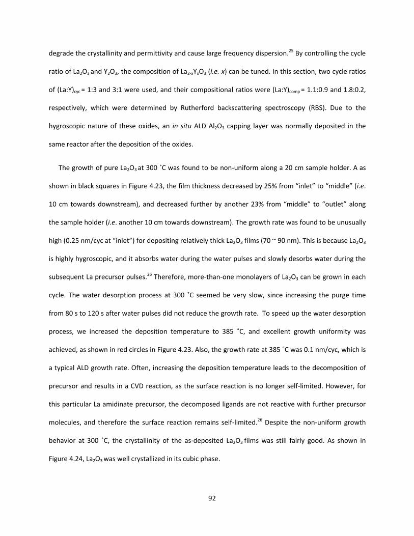
92
degrade the crystallinity and permittivity and cause large frequency dispersion.25 By controlling the cycle
ratio of La2O3 and Y2O3, the composition of La2-xYxO3 (i.e. x) can be tuned. In this section, two cycle ratios
of (La:Y)cyc = 1:3 and 3:1 were used, and their compositional ratios were (La:Y)comp = 1.1:0.9 and 1.8:0.2,
respectively, which were determined by Rutherford backscattering spectroscopy (RBS). Due to the
hygroscopic nature of these oxides, an in situ ALD Al2O3 capping layer was normally deposited in the
same reactor after the deposition of the oxides.
The growth of pure La2O3 at 300 ˚C was found to be non-uniform along a 20 cm sample holder. A as
shown in black squares in Figure 4.23, the film thickness decreased by 25% from “inlet” to “middle” (i.e.
10 cm towards downstream), and decreased further by another 23% from “middle” to “outlet” along
the sample holder (i.e. another 10 cm towards downstream). The growth rate was found to be unusually
high (0.25 nm/cyc at “inlet”) for depositing relatively thick La2O3 films (70 ~ 90 nm). This is because La2O3
is highly hygroscopic, and it absorbs water during the water pulses and slowly desorbs water during the
subsequent La precursor pulses.26 Therefore, more-than-one monolayers of La2O3 can be grown in each
cycle. The water desorption process at 300 ˚C seemed be very slow, since increasing the purge time
from 80 s to 120 s after water pulses did not reduce the growth rate. To speed up the water desorption
process, we increased the deposition temperature to 385 ˚C, and excellent growth uniformity was
achieved, as shown in red circles in Figure 4.23. Also, the growth rate at 385 ˚C was 0.1 nm/cyc, which is
a typical ALD growth rate. Often, increasing the deposition temperature leads to the decomposition of
precursor and results in a CVD reaction, as the surface reaction is no longer self-limited. However, for
this particular La amidinate precursor, the decomposed ligands are not reactive with further precursor
molecules, and therefore the surface reaction remains self-limited.26 Despite the non-uniform growth
behavior at 300 ˚C, the crystallinity of the as-deposited La2O3 films was still fairly good. As shown in
Figure 4.24, La2O3 was well crystallized in its cubic phase.

93
Inlet Middle Outlet0.0
0.2
0.4
0.6
0.8
1.0
1.2
300 C
385 CRela
tive t
hic
kness
Figure 4.23. Uniformity of the La2O3 deposition at 300 ˚C (black squares) and 385 ˚C (red circles) along a 20 cm sample holder. The “inlet” and “outlet” samples were 20 cm apart, and the film thicknesses were normalized to those of the corresponding “inlet”
samples.
Figure 4.24. (a) TEM image of a ~ 70 nm La2O3 film deposited at 300 ˚C on a SiNx TEM grid with a 6 nm Al2O3 capping layer. (b) The corresponding electron diffraction
pattern indicated that the La2O3 was a cubic phase. The discrete spots in the diffraction pattern belong to the Si grid.

94
The depositions of Y2O3 and La2-xYxO3 (x = 0.2 or 0.9) were both performed at 300 ˚C, since Y2O3 is not
moisture sensitive, and in fact, adding Y2O3 into La2O3 to form La2-xYxO3 can significantly enhance the
moisture resistance of La2O3.28 The oxide crystallinity was also examined by TEM. As shown in Figure
4.25, a ~ 15 nm as-deposited Y2O3 film showed a well crystallized cubic-phase structure. The lattice
constant of cubic Y2O3 is ~ 6% smaller than that of cubic La2O3, and this difference was clearly observed
by comparing the relative positions of their (440) rings with respect to the reference Si (220) spots in
each of the diffraction patterns, respectively (Figure 4.24(b) and Figure 4.25(b)). Figure 4.26 showed the
TEM results of a ~ 40 nm as-deposited La1.8Y0.2O3 film. The film was well crystallized in one cubic phase,
indicating that 10% Y2O3 is soluble in cubic La2O3. According to the Vegard’s law, the lattice constant of
La1.8Y0.2O3 was expected to be ~ 0.6% smaller than that of La2O3. And this was qualitatively confirmed by
comparing their electron diffraction patterns (Figure 4.24(b) and Figure 4.26(b)), though a quantitative
comparison is difficult due to the limited resolution in TEM.
Figure 4.25. (a) TEM image of a ~ 15 nm Y2O3 film deposited at 300 ˚C on a SiNx TEM grid with a 6 nm Al2O3 capping layer. (b) The corresponding electron diffraction
pattern indicated that the Y2O3 was a cubic phase. The discrete spots in the diffraction pattern belong to the Si grid.

95
Figure 4.26. (a) TEM image of a ~ 40 nm La1.8Y0.2O3 film deposited at 300 ˚C on a SiNx TEM grid with a 4 nm Al2O3 capping layer. (b) The corresponding electron diffraction
pattern indicated that the La1.8Y0.2O3 was a cubic phase. The discrete spots in the diffraction pattern belong to the Si grid.
As the dielectric layers in MOSFETs are usually fairly thin, we also studied the crystallinity of 8 nm
films of these oxides in the following. The 8 nm films were deposited with the same ALD recipe as
previously: except for the pure La2O3 films which were deposited at 385 ˚C in this work, all the other
films were deposited at 300 ˚C, and all the films were capped with a 6 nm layer of in situ ALD Al2O3. The
TEM micrographs and the electron diffraction (ED) patterns of these films are shown in Figure 4.27. Both
of the pure La2O3 and La1.8Y0.2O3 films showed crystalline grains in the TEM images and clear ring
patterns in the ED patterns. On the other hand, for the La1.1Y0.9O3 film, indeed there were observable
crystalline grains in the image, but the crystalline features were only sparsely scattered and the majority
part of the film seemed to be amorphous. Thus, consequently, the rings in the ED pattern were weak
and blurry as shown in Figure 4.27(f). We also noticed that the ring labeled as “(440)” in the ED pattern
was a single ring, and its relative position with respective to the reference Si (220) spots was consistent
with the prediction of cubic La1.1Y0.9O3 from the Vegard’s law. This suggested that a crystalline oxide
alloy of La1.1Y0.9O3 could be formed, but it was only poorly crystallized under the current growth
conditions.

96
Figure 4.27. TEM images of 8 nm (a) La2O3, (b) La1.8Y0.2O3 and (c) La1.1Y0.9O3 films grown on SiNx TEM grids with the same ALD recipes as previously. (d), (e) and (f) are the
corresponding electron diffraction patterns, respectively. The discrete spots in the diffraction patterns belong to the Si grid.

97
4.3.2 Epitaxy of La2O3, Y2O3 and La2-xYxO3 on GaAs (111)A
The La2O3, Y2O3 and La2-xYxO3 (x = 0.2 or 0.9) films were also deposited on GaAs(111)A substrates.
Before deposition, all of the GaAs substrates were first dipped into a 3M HCl solution to remove the
native oxide and then soaked in a 10% (NH4)2S solution for 20 min for S-passivation. The oxides grown
on GaAs(111)A were found to be highly epitaxial, which was similar as the previously reported
LaLuO3/GaAs case.30 A cross-sectional TEM image of the La1.8Y0.2O3/GaAs(111)A interface is shown in
Figure 4.28(a). The epitaxial oxide/GaAs interface was flat and sharp, and a twin boundary relation was
clearly observed. The twin relation was also confirmed by the selective area electron diffraction pattern
as shown in Figure 4.28(b), where the two sets of diffraction patterns belonging to cubic-phase
La1.8Y0.2O3 and GaAs were well vertically aligned. Especially, the diffraction spot of GaAs (111)
overlapped with the La1.8Y0.2O3 (222) spot, suggesting that the lattice constants of these two materials
were very close. Unfortunately, TEM does not have enough resolution to further determine the tiny
difference in their lattice constants.
The epitaxy structures of these oxides on GaAs(111)A were further investigated by high-resolution X-
ray diffraction (HRXRD). In HRXRD, we use the reflection peaks from the GaAs substrate as the internal
reference, and focus on the relative shifts of the film peaks with respective to the GaAs substrate peaks,
since the shift in HRXRD is a more accurately measurable quantity. Also, we assume that our epitaxial
oxide films are relaxed with no strain.30 Then, the lattice mismatch for each oxide, defined as (aoxide –
2aGaAs)/2aGaAs, can be calculated from the observed relative shift.

98
Figure 4.28. (a) Cross-sectional TEM image of La1.8Y0.2O3/GaAs(111)A interface, and (b) the corresponding electron diffraction pattern with [01-1] beam direction.
We first examined the La2O3/GaAs(111)A samples. A 90 nm La2O3 film was deposited on a S-
passivated GaAs substrate by ALD with 364 cycles at 300 ˚C, and then followed by ALD of a 6 nm in situ
Al2O3 capping layer. The coupled 2-ω HRXRD scan was performed around the GaAs (111) reflection. As
shown in the red curve in Figure 4.29(a), there were multiple small peaks beside the strong GaAs (111)
substrate peak, at ~ 27.31˚. However, we believe that all these small peaks belong to the thickness
fringes (or Laue oscillations) of the film, and the main peak of La2O3 (222) overlapped with the strong
(111) peak of the GaAs substrate. We will validate this point by several methods in the following. But,

99
nevertheless, the well-defined Laue oscillations shown in the curve clearly revealed that a high-quality
epitaxial La2O3 film was successfully grown on GaAs(111)A.
Figure 4.29. (a) HRXRD coupled 2-ω scan of a 90 nm La2O3 film grown on GaAs(111)A (with a 6 nm Al2O3 capping layer), comparing with a simulated diffraction curve from
LEPTOS. (Lattice mismatch used in simulation was +0.037% for La2O3/GaAs.) (b)
Comparison of the 2-ω scans of the 90 nm La2O3 film and another thinner (70 nm) La2O3 film.
The periodicity of the Laue oscillations is determined by the film thickness, and the shift of the
oscillation pattern corresponds to the crystal lattice constant (i.e. the 2 angle of the main peak). We
performed a rough LEPTOS (Bruker) simulation to match up the positions of the Laue oscillations, as also
shown in Figure 4.29(a). The parameter of the film thickness in the simulation was 90 nm, which was
consistent with the measured thickness from XRF. The lattice constants used in the simulation were
a(La2O3) = 1.13102 nm and a(GaAs) = 0.5653 nm, suggesting a lattice mismatch of +0.037% for La2O3
with respect to GaAs. Again, we would like to emphasize that it is the lattice mismatch that is more
important than the absolute values of the lattice constants, and in fact, HRXRD is not capable of
measuring the absolute values of the lattice constants to such a high accuracy. From the estimated
mismatch of +0.037%, the 2 angle of the main peak of La2O3 (222) was calculated to be only 0.01˚

100
smaller than that of GaAs (111), and this difference is apparently too tiny to be resolved by any means.
In addition, the intensity of the film oscillations was not correctly simulated as shown in Figure 4.29(a).
This is because we did not consider many other complicated factors in the simulation, such as point
defect density, surface roughness, corrections to atomic scattering factors, etc.
To further check the statement that all of the small peaks in Figure 4.29(a) belong to the film
thickness fringes, we prepared another La2O3/GaAs(111)A sample with a thinner (70 nm) La2O3 layer.
This 70 nm La2O3 sample was expected to have the same 2 angle of the main peak of La2O3 (222), but
with a larger periodicity of the thickness fringes. The HRXRD scan of the 70 nm La2O3 sample was shown
in Figure 4.29(b), along with the previous scan of the 90 nm La2O3 sample for comparison. Clearly, all of
the small peaks shifted in a direction away from the GaAs (111) substrate peak, suggesting that none of
these peaks belong to the main peak of La2O3 (222). By careful comparing of the magnitudes of the shifts
for each pair of the oscillations, the Laue oscillation orders could be determined as labeled in Figure
4.29(b). Therefore, the main peak of La2O3 (222) was in overlapping with the strong GaAs (111) substrate
peak.
To further validate the magnitude of lattice mismatch, we also performed the coupled 2-ω HRXRD
scan around the GaAs (333) peak, since high-order diffraction usually has a larger peak splitting. As
shown in Figure 4.30, the La2O3 (666) peak appeared just at the shoulder of the GaAs (333) substrate
peak. Though, these two peaks were still very close and an accurate 2 angle of La2O3 (666) was difficult
to obtain, we were at least able to distinguish the La2O3 (666) peak from the strong GaAs (333) substrate
peak. The difference between the two 2 angles of these peaks was estimated to be around -0.046˚,
which corresponded to a lattice mismatch of ~ +0.040% for La2O3 with respective to GaAs. Since this
estimated value was fairly close to that from the previous simulation (i.e. +0.037%), we believe that we

101
are safe to conclude that the cubic La2O3 was in good lattice match with GaAs, with a lattice mismatch of
only +0.037%.
Figure 4.30. (a) HRXRD coupled 2-ω scan of the La2O3/GaAs(111)A sample around GaAs (333) reflection, and (b) a scan with doubled collecting time in a narrower region
for a better signal-to-noise ratio.
The heteroepitaxy structure of La1.8Y0.2O3/GaAs was also evaluated by HRXRD. The La1.8Y0.2O3/GaAs
sample has a 45 nm La1.8Y0.2O3 film grown at 300 ˚C on a S-passivated GaAs(111)A substrate with a 4 nm
Al2O3 capping layer on top. As the coupled 2-ω scan shown in Figure 4.31, the La1.8Y0.2O3 (222) peak and
the substrate GaAs (111) peak were too close to obtain an accurate 2 value of the La1.8Y0.2O3 (222)
reflection. But at least, an obvious shift of the film (222) peak towards larger 2 angle direction was
observed, indicating that Y2O3 was successfully mixed into the La2O3 lattice structure. In order to find out
the accurate 2 angle of the La1.8Y0.2O3 (222) reflection, we also performed a 2-Δω reciprocal space
mapping (RSM) around the GaAs (111) reflection on this sample. The reciprocal space maps are shown
in Figure 4.32, where the contour levels in (a) are in a logarithm color scale and the contour levels in (b)
are chosen to highlight the peaks. The 2 angle of the La1.8Y0.2O3 (222) reflection was found to shift by
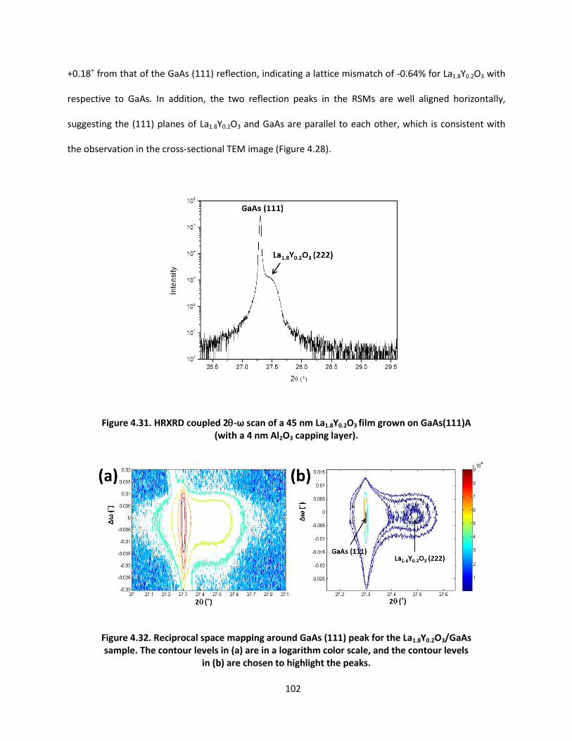
102
+0.18˚ from that of the GaAs (111) reflection, indicating a lattice mismatch of -0.64% for La1.8Y0.2O3 with
respective to GaAs. In addition, the two reflection peaks in the RSMs are well aligned horizontally,
suggesting the (111) planes of La1.8Y0.2O3 and GaAs are parallel to each other, which is consistent with
the observation in the cross-sectional TEM image (Figure 4.28).
Figure 4.31. HRXRD coupled 2-ω scan of a 45 nm La1.8Y0.2O3 film grown on GaAs(111)A (with a 4 nm Al2O3 capping layer).
Figure 4.32. Reciprocal space mapping around GaAs (111) peak for the La1.8Y0.2O3/GaAs sample. The contour levels in (a) are in a logarithm color scale, and the contour levels
in (b) are chosen to highlight the peaks.

103
Figure 4.33. HRXRD (a) coupled 2-ω scan and (b and c) rocking scans of a 21 nm La1.1Y0.9O3 film grown on GaAs(111)A (with a 4 nm Al2O3 capping layer).
Then we performed the HRXRD measurement on a La1.1Y0.9O3/GaAs sample, which had more Y
content than the La1.8Y0.2O3 case. The La1.1Y0.9O3/GaAs sample has a 21 nm La1.1Y0.9O3 film grown at 300
˚C on a S-passivated GaAs(111)A substrate with a 4 nm Al2O3 capping layer on top. The coupled 2-ω
scan is shown in Figure 4.33(a), where clear thickness fringes are shown, suggesting a high quality of
heteroepitaxy. Also, the film peak and the substrate peak were well separated in this case, with a
difference of +0.958˚ in 2 angle, which corresponded to a lattice mismatch of -3.32% for La1.1Y0.9O3 with
respect to GaAs. We also performed ω scans (rocking scans) for the La1.1Y0.9O3 (222) and GaAs (111)
peaks,f and the rocking curves are shown in Figure 4.33(b) and (c), respectively. The full width at half
maximum of the La1.1Y0.9O3 (222) rocking curve was the same as that of the GaAs (111) rocking curve (i.e.
~32”), which also indicated a high quality heteroepitaxy of La1.1Y0.9O3 on GaAs(111)A. Compared with the
case of ALD on amorphous substrates, where increasing the Y content resulted in the difficulty of
crystallization (Figure 4.27), depositing La2-xYxO3 on GaAs(111)A substrates did not exhibit the same
f Analyzer crystal was inserted for sharper peaks when measuring the rocking curves in HRXRD.

104
trend, despite that the ALD recipes were the same. This is likely because, in the initial growth stage, the
GaAs(111)A substrate lowers the barrier energy of the initial crystallization by forming a well arranged
layer of O atoms, which are bonded to the surface Ga atoms on the substrate, and meanwhile the
substrate also stabilizes the symmetry-matched cubic phase in the later growth stage.
Figure 4.34. HRXRD coupled 2-ω scan of a 12 nm Y2O3 film grown on GaAs(111)A (with a 6 nm Al2O3 capping layer).
We also performed the HRXRD measurement on a pure Y2O3/GaAs sample, which consisted of a 12
nm Y2O3 film grown at 300 ˚C on a S-passivated GaAs(111)A substrate with a 6 nm Al2O3 capping layer on
top. As the coupled 2-ω scan shown in Figure 4.34, the well-defined Y2O3 (222) peak along with a clear
thickness fringe on the right indicated that the Y2O3/GaAs structure was also a high-quality
heteroepitaxial structure. The 2 angle of the Y2O3 (222) peak was +1.92˚ greater than that of the GaAs
(111) peak, which corresponded to a lattice mismatch of -6.44% for Y2O3 with respect to GaAs.

105
Table 4.3. Summary of lattice constants and mismatches of Y2O3, La1.1Y0.9O3, La1.8Y0.2O3, and La2O3.
Measured mismatch to GaAs
Mismatch estimated by Vegard’s law
Measured lattice constant a (nm)g
Lattice constant from references
a (nm)
Y2O3 -6.44% 1.0579 1.0604h
La1.1Y0.9O3 -3.32% -2.88% 1.0931
La1.8Y0.2O3 -0.64% -0.61% 1.1234
La2O3 +0.037% 1.1310 1.1327i
So far, we have shown that epitaxial Y2O3, La1.1Y0.9O3, La1.8Y0.2O3, and La2O3 thin films were
successfully grown on GaAs(111)A substrates by ALD. Both cross-sectional TEM and HRXRD have
revealed a high-quality cubic-on-cubic heteroepitaxy relation of the oxide/GaAs with a fully relaxed
interface. The lattice mismatches of oxide/GaAs were measured by HRXRD, and the values are listed in
Table 4.3. The HRXRD also indicated that Y2O3 and La2O3 formed a good alloy for the tested composition
ratios. The atomic ratios of La:Y in La1.1Y0.9O3 and La1.8Y0.2O3 were further confirmed by RBS.j The lattice
mismatches estimated by the Vegard’s law were reasonably close to the measured values (Table 4.3).
Since the oxide/GaAs epitaxial interface is a fully relaxed interface, the requirement for lattice mismatch
is less strict for the epitaxy to occur. Therefore, we believe that the heteroepitaxy can occur with any
La:Y ratios, since the two extreme cases (pure Y2O3 and pure La2O3) were both confirmed to be epitaxial.
In addition, as HRXRD examines the epitaxy over a several-mm2 area, our results also indicated that the
high quality epitaxy occurred over a fairly large area, which is promising for large-scale processes.
Moreover, the above observations of La2-xYxO3/GaAs(111)A (x = 0, 0.2, 0.9 and 2) are quite similar as in
our previous studies of the heteroepitaxy of LaLuO3/GaAs(111)A, where the LaLuO3 film was grown by a
g Assuming aGaAs = 0.56535 nm, the oxide lattice constants were calculated from the mismatches.
h PDF 00-041-1105
i PDF 00-022-0369
j RBS was run in random mode for avoiding the channeling effect.

106
similar ALD process.30 As Y is a relatively more abundant element than Lu, La2-xYxO3 might be a good
alternative for LaLuO3.
4.3.3 Electrical properties of La2-xYxO3/GaAs(111)A (x = 0.2 and 0.9)
The electrical properties of the La2-xYxO3/GaAs(111)A (x = 0.2 and 0.9) structures were characterized
by Lin Dong in Prof. Peide D. Ye’s group at Purdue University. P-type GaAs(111)A wafers with a doping
concentration of 5 ~ 7 × 1017 cm-3 were used as the substrates for fabricating p-MOS capacitors. The
GaAs surface was treated with S-passivation before growing the dielectric layer by ALD. The dielectric
layer consisted of a 7.5 nm La2-xYxO3 layer, with an in situ capping layer of 6.5 nm Al2O3 on top. The oxide
deposition was performed at 300 ˚C with the recipe described in Section 4.3.1. After the dielectric
deposition, the samples were treated with rapid-thermal-annealing (RTA) at 800 ˚C for 30 seconds in N2
ambient. Then Ni/Au circular metal electrodes were patterned and evaporated to make p-MOS
capacitors.
We first evaluated the capacitance-voltage (C-V) characteristics of the p-MOS capacitors, each of
which consisted a stack of Ni/6.5 nm Al2O3/7.5 nm La2-xYxO3/p-GaAs(111)A (x = 0.2 or 0.9). As shown in
Figure 4.35, the C-V characteristics were nearly ideal, as the frequency dispersions were 1.0% and 1.8%
on the accumulation side and the flatband shifts were 0.095 V and 0.103 V between 1 kHz and 1 MHz for
La1.1Y0.9O3 and La1.8Y0.2O3, respectively. These values were significantly smaller than those of
LaLuO3/GaAs(111)A in the previous report, i.e. 9% in frequency dispersion and 0.2 V in flatband shift,30
which indicated that a much better interface quality was achieved by using La2-xYxO3 as the dielectric
oxide. A closer comparison of the C-V curves at 100 kHz (Figure 4.35(c)) revealed that the C-V curve for
La1.8Y0.2O3 is less “stretched-out” than the curve for La1.1Y0.9O3, suggesting a relatively smaller interfacial
trap density (Dit) for La1.8Y0.2O3/GaAs(111)A. The effective oxide thicknesses (EOTs) extracted from the C-
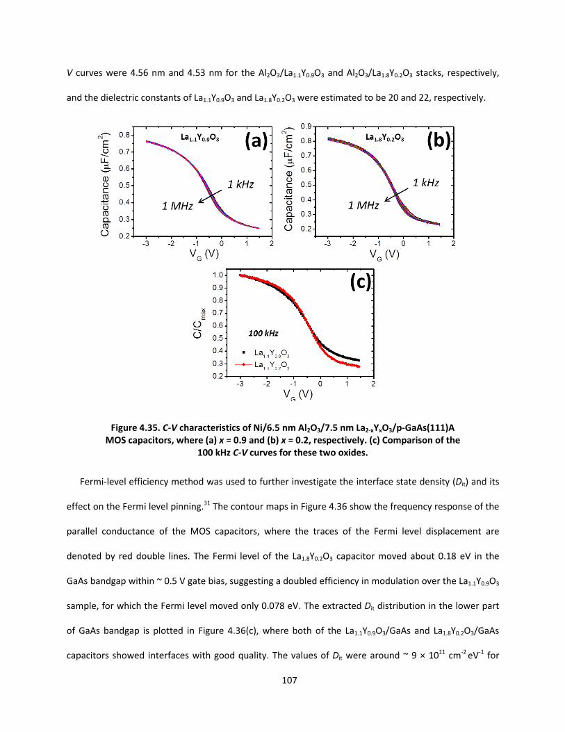
107
V curves were 4.56 nm and 4.53 nm for the Al2O3/La1.1Y0.9O3 and Al2O3/La1.8Y0.2O3 stacks, respectively,
and the dielectric constants of La1.1Y0.9O3 and La1.8Y0.2O3 were estimated to be 20 and 22, respectively.
Figure 4.35. C-V characteristics of Ni/6.5 nm Al2O3/7.5 nm La2-xYxO3/p-GaAs(111)A MOS capacitors, where (a) x = 0.9 and (b) x = 0.2, respectively. (c) Comparison of the
100 kHz C-V curves for these two oxides.
Fermi-level efficiency method was used to further investigate the interface state density (Dit) and its
effect on the Fermi level pinning.31 The contour maps in Figure 4.36 show the frequency response of the
parallel conductance of the MOS capacitors, where the traces of the Fermi level displacement are
denoted by red double lines. The Fermi level of the La1.8Y0.2O3 capacitor moved about 0.18 eV in the
GaAs bandgap within ~ 0.5 V gate bias, suggesting a doubled efficiency in modulation over the La1.1Y0.9O3
sample, for which the Fermi level moved only 0.078 eV. The extracted Dit distribution in the lower part
of GaAs bandgap is plotted in Figure 4.36(c), where both of the La1.1Y0.9O3/GaAs and La1.8Y0.2O3/GaAs
capacitors showed interfaces with good quality. The values of Dit were around ~ 9 × 1011 cm-2 eV-1 for

108
La1.1Y0.9O3/GaAs(111)A and ~ 5 × 1011 cm-2 eV-1 for La1.8Y0.2O3/GaAs(111)A, respectively, which are
roughly one order of magnitude lower than that of the Al2O3/GaAs(111)A interface.30 These results
support the point that having an epitaxial dielectric layer lowers the interface state density. Moreover,
the interface quality of La1.8Y0.2O3/GaAs(111)A was comparatively better than that of
La1.1Y0.9O3/GaAs(111)A, suggesting that matching the lattice constants of the oxide and the substrate
could provide further improvement for interface quality.
Figure 4.36. Frequency response of the parallel conductance of (a) La1.1Y0.9O3/GaAs and (b) La1.8Y0.2O3/GaAs MOS-capacitors. (c) Dit distribution in the lower part of GaAs
bandgap.

109
We further performed some preliminary tests on transistor performance with La1.8Y0.2O3 as the
dielectric oxide. Semi-insulating GaAs wafers were used for fabricating GaAs NMOSFETs. An oxide stack
of 7.5 nm La1.8Y0.2O3 and 6.5 nm Al2O3 (EOT ~ 4.5 nm) was deposited on S-passivated GaAs substrates
with the same method as for MOS capacitors. Then the oxide/GaAs samples were ion implanted with Si
to create n+ doping areas, followed by RTA dopant activation at 860 ˚C for 15 s in N2, source/drain
contact patterning and oxide removal, source/drain ohmic contact metal (GeNi/Au) evaporation and
RTA at 400 ˚C for 30 s in N2, and gate patterning and gate metal (Ni/Au) evaporation, to make the final
NMOSFET devices. The results of the electrical characterizations of a 0.5µm-gate-length inversion-mode
GaAs(111)A NMOSFET with Al2O3/La1.8Y0.2O3 gate dielectric were shown in Figure 4.37. The output
characteristics exhibited a substantially high maximum drain current of 326 mA/mm with VDS = 2V and
VGS = 5V, as shown in Figure 4.37(a), and the transfer characteristics showed a fairly low subthreshold
swing (SS) of 97 mV/dec. This low SS value was further confirmed by the measurements on multiple
devices with various gate lengths from 0.5 μm to 40 μm. The low SS also suggested that the
La1.8Y0.2O3/GaAs interface had a fairly low mid-gap Dit.
Figure 4.37. (a) Output characteristics (IDS ~ VDS) and (b) transfer characteristics (IDS ~ VGS) of a LG = 0.5 μm GaAs(111)A NMOSFET with Al2O3/La1.8Y0.2O3 gate dielectric. The
device gate leakage current (JG) is also plotted in (b).

110
4.3.4 Summary and future prospects
So far, we have demonstrated that La2-xYxO3 (x = 0, 0.2, 0.9 and 2) films can be epitaxially grown on
GaAs(111)A substrates by our ALD process. The quality of this heteroepitaxy was fairly high as revealed
by cross-sectional TEM and HRXRD. We have also fabricated the La2-xYxO3/GaAs(111)A (x = 0.2 and 0.9)
MOS capacitors to evaluate the electrical properties of the La2-xYxO3/GaAs(111)A interface. Both
La1.8Y0.2O3 and La1.1Y0.9O3 showed fairly low Dit on GaAs(111)A substrates. Comparatively, La1.8Y0.2O3/GaAs
showed even lower Dit than La1.1Y0.9O3/GaAs, suggesting that closer lattice-mismatch provides interfaces
with better quality. Utilizing the Al2O3/La1.8Y0.2O3 stack as the dielectric layer, high performance
GaAs(111)A NMOSFETs were demonstrated. Our preliminary characterizations suggested that the
epitaxial dielectric layer of La2-xYxO3 is very promising for III-V MOSFET applications. We believe these
new results will extent the ~50-year research on oxide/GaAs interface to an unprecedented level.
Pure La2O3 is also promising as the dielectric material on GaAs(111)A, since it has an even smaller
lattice mismatch of +0.037%, compared with La1.8Y0.2O3 (-0.64%), with respect to GaAs. As the mismatch
is smaller by a factor of 17, assuming Dit is proportional to the density of the un-passivated surface
dangling bonds, which is proportional to the square of mismatch, pure La2O3 is expected to further
lower the Dit by a factor of ~ 290 with respect to La1.8Y0.2O3. However, pure La2O3 is more challenging to
grow due to its highly hygroscopic nature.
On the other hand, La2-xYxO3 may also be used on other III-V substrates, such as InP and InGaAs. As
our preliminary HRXRD results shown in Figure 4.38, La1.8Y0.2O3 can also be epitaxially grown on a
InP(111)A substrate with a fully relaxed high-quality epitaxy. However, as InP has a lattice constant
about 3.8% larger than GaAs, La2-xYxO3 is not capable of matching the InP lattice perfectly. But still, we
expect that the interface quality will be improved by introducing an epitaxial dielectric oxide layer.

111
As we have shown the epitaxial growth of La2-xYxO3 in this work, along with the epitaxial growth of
LaLuO3 in our group’s previous work,30 it is natural to speculate that other lanthanoid oxides may also be
epitaxially grown on GaAs(111)A in a similar way. If it is proven to be true, we may have more flexibility
in choosing the lanthanoid oxides (or Y2O3) to balance other factors, such as earth abundance, price,
easiness for ALD, etc.
Lastly, usually the (100) orientation is preferred for III-V devices, since the (100) substrates are more
available than the (111) substrates. It would be a great improvement, if epitaxial oxide films could also
be grown on the (100)-oriented III-V substrates. However, our initial studies seemed to suggest that it is
quite challenging for epitaxial growth to occur on the (100) substrates, since the (100) surface has two
degenerated directions for crystal growth, which usually leads to growing polycrystalline films.32 Further
investigation is needed in this regard.
Figure 4.38. HRXRD coupled 2-ω scan of a 45 nm La1.8Y0.2O3 film grown on InP(111)A (with a 4 nm Al2O3 capping layer).

112
4.4 References
1 X. J. Huang, et al., Ieee Transactions on Electron Devices 48, 880 (2001).
2 Solid State Technol. 49, 28 (2006).
3 N. Singh, et al., IEEE Electron Device Lett. 27, 383 (2006).
4 J. J. Gu, Y. Q. Liu, Y. Q. Wu, R. Colby, R. G. Gordon, P. D. Ye, and Ieee, First Experimental
Demonstration of Gate-all-around III-V MOSFETs by Top-down Approach, 2011).
5 C. Bae, H. Shin, and K. Nielsch, Mrs Bulletin 36, 887 (2011).
6 M. Leskela, M. Ritala, and O. Nilsen, Mrs Bulletin 36, 877 (2011).
7 G. N. Parsons, S. M. George, and M. Knez, Mrs Bulletin 36, 865 (2011).
8 Z. W. Li, A. Rahtu, and R. G. Gordon, J. Electrochem. Soc. 153, C787 (2006).
9 T. Aaltonen, M. Ritala, T. Sajavaara, J. Keinonen, and M. Leskela, Chem. Mat. 15, 1924 (2003).
10 B. S. Lim, A. Rahtu, and R. G. Gordon, Nature Materials 2, 749 (2003).
11 J. S. Becker, S. Suh, S. L. Wang, and R. G. Gordon, Chem. Mat. 15, 2969 (2003).
12 R. L. Puurunen, J. Appl. Phys. 97 (2005).
13 P. D. X. Ye, Yi; Wu, Yanqing; Xu, Min, in Fundamentals of III-V semiconductor MOSFETs, edited by
S. Y. Oktyabrsky, Peide D (Springer, 2010).
14 B. S. Lim, A. Rahtu, P. de Rouffignac, and R. G. Gordon, Appl. Phys. Lett. 84, 3957 (2004).
15 H. Wang, Harvard University, 2009.
16 J. J. Gu, W. Heng, L. Yiqun, A. T. Neal, R. G. Gordon, and P. D. Ye, Electron Device Letters, IEEE 33,
967 (2012).
17 M. Radosavljevic, et al., Electrostatics Improvement in 3-D Tri-gate Over Ultra-Thin Body Planar
InGaAs Quantum Well Field Effect Transistors with High-K Gate Dielectric and Scaled Gate-to-
Drain/Gate-to-Source Separation, 2011).

113
18 K. Tomioka, M. Yoshimura, T. Fukui, and Ieee, Vertical In0.7Ga0.3As Nanowire Surrounding-Gate
Transistors with High-k Gate Dielectric on Si Substrate, 2011).
19 A. W. Dey, C. Thelander, E. Lind, K. A. Dick, B. M. Borg, M. Borgstrom, P. Nilsson, and L. E.
Wernersson, Electron Device Letters, IEEE 33, 791 (2012).
20 C. Hock-Chun, G. Xiao, W. Lanxiang, L. Hock Koon, S. Luping, and Y. Yee-Chia, Electron Device
Letters, IEEE 32, 146 (2011).
21 S. H. Kim, et al., in VLSI Technology (VLSIT), 2012 Symposium on, 2012), p. 177.
22 L. K. Bera, et al., Three dimensionally stacked SiGe nanowire array and Gate-All-Around p-
MOSFETs (Ieee, New York, 2006).
23 W. W. Fang, N. Singh, L. K. Bera, H. S. Nguyen, S. C. Rustagi, G. Q. Lo, N. Balasubramanian, and D.
L. Kwong, IEEE Electron Device Lett. 28, 211 (2007).
24 Y. H. Wu, M. Y. Yang, A. Chin, W. J. Chen, and C. M. Kwei, IEEE Electron Device Lett. 21, 341
(2000).
25 Y. Zhao, M. Toyama, K. Kita, K. Kyuno, and A. Toriumi, Appl. Phys. Lett. 88 (2006).
26 J. Kwon, M. Dai, M. D. Halls, E. Langereis, Y. J. Chabal, and R. G. Gordon, J. Phys. Chem. C 113,
654 (2009).
27 M. Suzuki, Materials 5, 443 (2012).
28 Y. Zhao, K. Kita, K. Kyuno, and A. Toriumi, Appl. Phys. Lett. 89 (2006).
29 P. de Rouffignac, J.-S. Park, and R. G. Gordon, Chem. Mat. 17, 4808 (2005).
30 Y. Liu, M. Xu, J. Heo, P. D. Ye, and R. G. Gordon, Appl. Phys. Lett. 97 (2010).
31 H. C. Lin, G. Brammertz, K. Martens, G. de Valicourt, L. Negre, W. E. Wang, W. Tsai, M. Meuris,
and M. Heyns, Appl. Phys. Lett. 94 (2009).
32 Y. Q. Liu, Harvard University, 2011.

114
Chapter 5 Vapor Deposition of High-k materials for
GaN-Based HEMT Devices
Gallium-nitride-based high-electronmobility transistors (HEMTs) are considered to be suitable for
high frequency switches and high power devices. However, typical AlGaN/GaN HEMTs rely on Schottky
gates, which suffer from high gate leakage and impose a limit on the maximum gate bias that can be
applied. Applications for power electronics require low leakage in the off state and thus it is necessary to
fabricate devices with a gate dielectric. At the same time, AlGaN/GaN HEMTs suffer typically suffer from
current collapse, due to trap states on the AlGaN surface. One approach to mitigate the current collapse
is to grow a passivation layer of SiNx by plasma-enhanced chemical vapor deposition (PECVD).1 However,
its leakage is still not sufficiently low for power switching devices, and PECVD does not allow for precise
control of dielectric thickness. Another approach to passivate the surface is to grow a high-k oxide layer,
such as Al2O3 or HfO2.1, 2 These oxides have very low leakage, and their high-k property guarantees that
the channel modulation can be effectively controlled by the gate. In addition, these oxide thin layers can
be prepared by atomic layer deposition (ALD), which is known for making ultra-smooth films with
precise control of the film thickness. Besides oxides, a recent report demonstrated that a thin AlN film,
which was prepared by plasma enhanced ALD (PEALD), could also effectively suppress the current
collapse.3
In this chapter, we will discuss the ALD processes of several candidate materials for the surface
passivation of the GaN devices, including AlN, MgO, Sc2O3, and some other oxides, and some preliminary
measurements of the electrical properties will be presented. The basic properties of these materials are
listed in Table 5.1. All of the listed dielectrics have high band gaps, which are beneficial for a low leakage
current and a high break-down field for the devices. The nitrogen component in AlN can possibly

115
minimize the nitrogen leaving from GaN in high-temperature processes. The MgO can be mixed with
CaO to form a lattice-matched alloy of Mg0.5Ca0.5O, which is potentially capable of passivating all the
dangling bonds on the GaN surface, and therefore minimize the interface state density. The bixbyite
Sc2O3 is also promising, as it has been grown epitaxially on GaN.4
Table 5.1. Material properties of GaN and various dielctrics.5
GaN AlN CaO MgO Mg0.5Ca0.5O Sc2O3
Structure Wurtzite Wurtzite NaCl NaCl NaCl Bixbyite
Lattice constant (Å) 3.186 3.133 4.799 4.2112 4.505 9.845
Atomic spacing in the (111) plane
3.393 2.978 3.186 3.4807
Mismatch to GaN (%) 2.3 6.6 -6.5 0 9.2
Tmp (K) 2800 3500 2860 3073 2678
Band gap (eV) 3.4 6.2 7 8 6.3
Electron affinity (eV) 3.4 0~2.9 0.7
Work Function (eV) 0.9~1.2 4 3.1~4.4 2.1~3.3
Dielectric constant 9.5 8.5 11.8 9.8 14
5.1 ALD of AlN
Aluminum nitride (AlN) has a wide direct band gap (6.2 eV), high thermal conductivity (285 W m−1
K−1),
low thermal expansion coefficient, and high decomposition temperature (2800 °C). It has been widely
used in III-nitride based microelectronic and optoelectronic devices. Very recently, a thin AlN layer has
been reported to be able to effectively suppress the current collapse in GaN-based devices.3 AlN films
have been deposited by chemical vapor deposition, reactive sputtering, pulsed laser deposition (PLD),
and molecular beam epitaxy (MBE). For most of the applications in microelectronics, besides having
good film quality, the precise control of film thickness is also very important, since usually only a few
nanometers of AlN films are needed in devices. ALD is considered as a good candidate serving this
purpose, as ALD films are usually dense, uniform, and pin-hole free, and the film thickness can be
precisely controlled by varying the cycle number. Also, comparing the instrumental cost of ALD with

116
MBE and PLD, the cost of ALD is much less, which recommends ALD as a promising deposition method
for AlN films. However, to the best of our knowledge, there is no thermal ALD process reported so far.
Only processes of plasma enhanced ALD (PEALD) with trimethylaluminum (TMA) and ammonia as the
reactants were reported.6-10 The reason of introducing plasma is that the ammonia itself has very little
reactivity with TMA, and therefore, high energy plasma is needed to break the N-H bonds to form
reactive species such as radicals and ions. However, with such a PEALD process, it is usually easy to
incorporate carbon impurities in the films, since the methyl groups in TMA are difficult to be completely
removed. As carbon impurities are known to be donors in the AlN band gap, too much carbon is likely to
deteriorate the optical properties of AlN.5 Also, the high-energy plasma may damage the surface of GaN
devices, which is another concern for PEALD. Therefore, a new ALD process to prepare carbon-free high-
quality AlN is needed.
In this section, we will report a thermal ALD process of AlN by using hexakis(dimethylamido)
dialuminum, Al2(N(CH3)2)6, as the aluminum source and ammonia as the nitrogen source. Compared with
other conventional aluminum precursors, such as TMA, Al2(N(CH3)2)6 does not have any direct Al-C
bonds, which can reduce the chance of carbon incorporation in films. Also, the byproduct
dimethylamine, HN(CH3)2, is a good leaving molecule. Back in early 1990s, our group reported a CVD
process of AlN with this precursor.11, 12 A comparison of the ALD and CVD AlN films will be followed as
well.
The AlN deposition was carried out in a home-built tubular reactor. The precursor, Al2(N(CH3)2)6, was
kept in sealed bubbler in a heated oven, and was delivered into the reaction chamber with N2 carrier gas.
The substrates were Si wafers. Each of them was treated with UV light for 5 minutes and then dipped
into the HF solution for 30 seconds before loaded into the reactor for AlN deposition. AlN films were
deposited at a temperature range from 220 °C to 235 °C. Film thickness was measured by X-ray
reflectometry (XRR). However, as will be discussed later, due to the immediate oxidation of AlN when
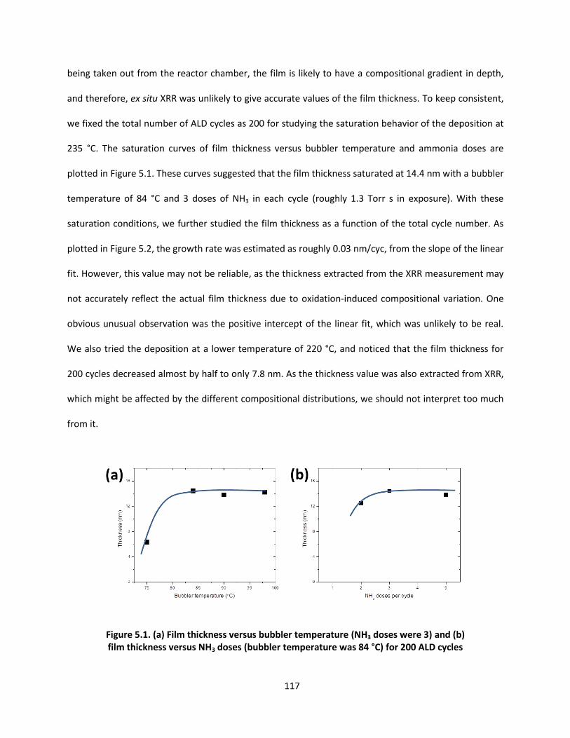
117
being taken out from the reactor chamber, the film is likely to have a compositional gradient in depth,
and therefore, ex situ XRR was unlikely to give accurate values of the film thickness. To keep consistent,
we fixed the total number of ALD cycles as 200 for studying the saturation behavior of the deposition at
235 °C. The saturation curves of film thickness versus bubbler temperature and ammonia doses are
plotted in Figure 5.1. These curves suggested that the film thickness saturated at 14.4 nm with a bubbler
temperature of 84 °C and 3 doses of NH3 in each cycle (roughly 1.3 Torr s in exposure). With these
saturation conditions, we further studied the film thickness as a function of the total cycle number. As
plotted in Figure 5.2, the growth rate was estimated as roughly 0.03 nm/cyc, from the slope of the linear
fit. However, this value may not be reliable, as the thickness extracted from the XRR measurement may
not accurately reflect the actual film thickness due to oxidation-induced compositional variation. One
obvious unusual observation was the positive intercept of the linear fit, which was unlikely to be real.
We also tried the deposition at a lower temperature of 220 °C, and noticed that the film thickness for
200 cycles decreased almost by half to only 7.8 nm. As the thickness value was also extracted from XRR,
which might be affected by the different compositional distributions, we should not interpret too much
from it.
Figure 5.1. (a) Film thickness versus bubbler temperature (NH3 doses were 3) and (b) film thickness versus NH3 doses (bubbler temperature was 84 °C) for 200 ALD cycles
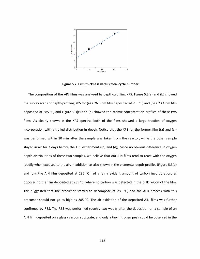
118
Figure 5.2. Film thickness versus total cycle number
The composition of the AlN films was analyzed by depth-profiling XPS. Figure 5.3(a) and (b) showed
the survey scans of depth-profiling XPS for (a) a 26.5 nm film deposited at 235 °C, and (b) a 23.4 nm film
deposited at 285 °C, and Figure 5.3(c) and (d) showed the atomic concentration profiles of these two
films. As clearly shown in the XPS spectra, both of the films showed a large fraction of oxygen
incorporation with a trailed distribution in depth. Notice that the XPS for the former film ((a) and (c))
was performed within 10 min after the sample was taken from the reactor, while the other sample
stayed in air for 7 days before the XPS experiment ((b) and (d)). Since no obvious difference in oxygen
depth distributions of these two samples, we believe that our AlN films tend to react with the oxygen
readily when exposed to the air. In addition, as also shown in the elemental depth-profiles (Figure 5.3(d)
and (d)), the AlN film deposited at 285 °C had a fairly evident amount of carbon incorporation, as
opposed to the film deposited at 235 °C, where no carbon was detected in the bulk region of the film.
This suggested that the precursor started to decompose at 285 °C, and the ALD process with this
precursor should not go as high as 285 °C. The air oxidation of the deposited AlN films was further
confirmed by RBS. The RBS was performed roughly two weeks after the deposition on a sample of an
AlN film deposited on a glassy carbon substrate, and only a tiny nitrogen peak could be observed in the

119
RBS spectrum (Figure 5.4). We believe that the oxidation tendency of our ALD AlN films is because the
films were not sufficiently dense.
Figure 5.3. Depth-profiling XPS analysis of AlN films deposited at 235 °C ((a) and (c)) and 285 °C ((b) and (d)).
Figure 5.4. RBS analysis of a 23 nm AlN deposited on a glassy carbon substrate. The RBS measured was performed after two weeks of air exposure.
0 200 400 600 800 1000
Channel
0
2
4
6
8
10
No
rmal
ized
Yie
ld
0.2 0.4 0.6 0.8 1.0 1.2
Energy (MeV)
N AlOC

120
The crystallinity of the AlN films deposited at 235 °C was examined by TEM as shown in Figure 5.5.
The TEM micrograph seemed to suggest that the film was just about to crystalize, and the diffuse ring
pattern in the electron diffraction pattern suggested that the grain size was very tiny. This was similar as
the films deposited by CVD at a similar deposition temperature.11, 12 However, unlike the CVD films,
annealing these ALD AlN films at 600 °C turned the films to a pure amorphous phase (not shown here).
This might be due to a trace amount of oxygen in the annealing ambient, which oxidized the films to
amorphous aluminum oxide. As higher deposition temperature usually gives better film crystallinity, we
also tried depositing AlN films at 385 °C. As shown in Figure 5.6, the TEM micrograph seemed to suggest
that the film had quite a large amount of carbon impurity, which inhibited the film from crystallization.
This is consistent with the previous XPS observation that the precursor decomposed at a deposition
temperature higher than 285 °C.
Figure 5.5. TEM (a) image and (b) electron diffraction pattern of a 14 nm AlN deposited on a SiNx TEM grid at 235 °C.
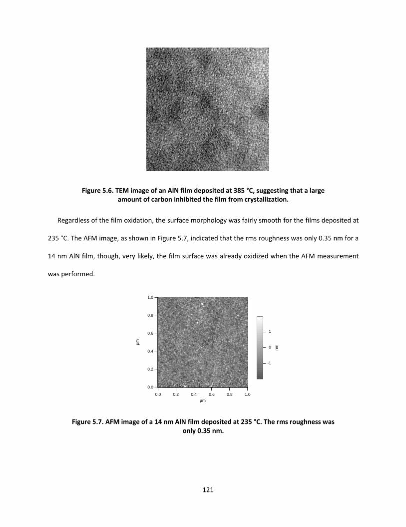
121
Figure 5.6. TEM image of an AlN film deposited at 385 °C, suggesting that a large amount of carbon inhibited the film from crystallization.
Regardless of the film oxidation, the surface morphology was fairly smooth for the films deposited at
235 °C. The AFM image, as shown in Figure 5.7, indicated that the rms roughness was only 0.35 nm for a
14 nm AlN film, though, very likely, the film surface was already oxidized when the AFM measurement
was performed.
Figure 5.7. AFM image of a 14 nm AlN film deposited at 235 °C. The rms roughness was only 0.35 nm.
1.0
0.8
0.6
0.4
0.2
0.0
µm
1.00.80.60.40.20.0
µm
-1
0
1
nm

122
Figure 5.8. TEM of AlN deposited by pulsed CVD at 335 °C. Both of the micrographs ((a) and (b) with different magnifications) and (c) the electron diffraction pattern showed
a much better crystalline structure compared with ALD AlN films.
In summary, an ALD process of AlN has been demonstrated in this work. However, the ALD AlN is
likely to have a low density, so that it would be easily oxidized by the air. The aluminum precursor,
Al2(N(CH3)2)6, showed decomposition behavior at 285 °C, which limits the highest temperature of the
corrsponding ALD process. Thus, a dense AlN film might be difficult to achieve with this precursor by
ALD. On the other hand, one might consider depositing AlN in a pulsed CVD mode. Preliminary tests
showed that the pulsed CVD could go up to 335 °C, and the film showed a much better crystalline
structure (Figure 5.8). Further experiments, such as measuring the carbon content, are needed to
investigate this pulsed CVD process.
5.2 ALD of MgO
MgO is a high band gap (8 eV) dielectric material with a dielectric constant of 9.8. Previous studies
have demonstrated that the MBE-grown MgO produces a relatively low interface state density on GaN
and is stable against high-temperature process, and therefore it is promising for high voltage and
current applications.13-15 Also, MgO has a smaller atomic spacing in its (111) plane comparing with the
atomic spacing in GaN (0001) plane (-6.5%). Thus, mixing MgO with CaO, which has a slightly larger
lattice constant (Table 5.1), with an atomic ratio of 1:1 can form an oxide alloy (i.e. Mg0.5Ca0.5O) with

123
zero lattice-mismatch to GaN (0001). A lattice-matched oxide is potentially capable to passivate all the
dangling bonds on the GaN surface, and therefore minimize the interface state density. One problem
with this binary oxide system is the large difference in ionic radius between Mg and Ca, which causes
severe immiscibility.5 To circumvent this issue, a low temperature deposition process which allows for
the formation of metastable phases is needed. ALD is a promising deposition method to achieve that,
since the deposition temperature is usually below 400 °C. Several ALD processes of MgO have been
reported with Mg(C2H5)2,16 Mg(Cp)2,
17-19 Mg(CpEt)2,20 or Mg(thd)2
21, 22 as the Mg precursor and H2O,16-20
H2O2,22 or O3
21 as the oxygen source. However, carbon impurity is always a concern for these Mg
precursors which have direct Mg-C bonds.19 In this section, we will discuss a new ALD process of MgO
using an amidinate Mg precursor, which does not have the direct Mg-C bonds. We expect this amidinate
precursor to produce carbon-free MgO films.
The ALD of MgO was carried out in a home-built reactor, with bis(N,N’-di-tert-butylacetamidinato)
magnesium and H2O as the precursors. The magnesium precursor was placed in a glass bubbler kept in a
heated oven at 115 °C. The deposition temperature varied from 258 °C to 332 °C. The film thickness was
characterized by XRR. Excellent uniformity of film thickness (within 2%) along a 20 cm sample holder
was achieved (Figure 5.9), suggesting a very good ALD growth behavior. The temperature dependence
of the growth rate was also measured as shown in (Figure 5.10). The growth rate slightly decreased as
the deposition temperature increased, which was also observed in another ALD process of MgO using
bis(N,N’-di-sec-butylacetamidinato) magnesium as the Mg precursor.k
k Kyoung Kim, unpublished results from our group.

124
Figure 5.9. Uniformity of MgO deposition along a 20 cm sample holder. The “inlet” and “outlet” samples were 20 cm apart, and the film thicknesses were normalized to those
of the corresponding “inlet” samples.
Figure 5.10. Growth rate of ALD MgO as a function of deposition temperature.
The MgO density, calculated from RBS and XRR data, was found to be the same as its bulk density (i.e.
3.58 g/cm3). The thermal decomposition of the Mg precursor was tested at 322 °C, which was the
highest deposition temperature we tried in this work. A deposition of pulsing 1500 doses of the Mg
precursor without pulsing H2O in between was performed on a glassy carbon substrate. Then the sample

125
was measured by RBS, and the decomposition rate was determined to be 0.0017 nm/cyc, which was
only 3.4 % of the normal growth rate. Therefore, we concluded that this precursor was quite stable in
our deposition temperature range, and it is suitable for our ALD process.
MgO thin films have shown evident degradation in ambient due to the formation and bonding of
several different species on the surface, mainly from the reactions with H2O and CO2.23, 24 A 4 nm ALD
Al2O3 capping layer was deposited in situ after the MgO deposition in the same reactor. A ~ 10 nm MgO
film with this Al2O3 capping layer was analyzed by depth-profiling XPS. As the survey scans and elemental
depth-profiles shown in Figure 5.11, the ALD MgO film was quite pure, especially with no detectable
carbon impurities. (The tailed elemental depth-distribution was likely due to the sputtering effect in the
depth-profiling XPS measurement.)
Figure 5.11. XPS depth profiling of a ~10 nm MgO with a 4 nm Al2O3 capping. (a) Survey scan spectra and (b) elemental depth-profile.
The crystallinity of the ALD MgO was examined by TEM. A ~ 10 nm MgO film was deposited on a SiNx
membrane TEM grid with an Al2O3 capping layer. The TEM micrograph (Figure 5.12(a)) showed
crystalline structures with an average grain size around 8 nm. The electron diffraction pattern (Figure
5.12(b)) showed sharp rings, which all belong to the cubic phase of MgO, suggesting that the film was
well crystalized in a pure MgO phase (especially no MgCO3).
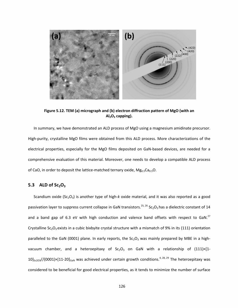
126
Figure 5.12. TEM (a) micrograph and (b) electron diffraction pattern of MgO (with an Al2O3 capping).
In summary, we have demonstrated an ALD process of MgO using a magnesium amidinate precursor.
High-purity, crystalline MgO films were obtained from this ALD process. More characterizations of the
electrical properties, especially for the MgO films deposited on GaN-based devices, are needed for a
comprehensive evaluation of this material. Moreover, one needs to develop a compatible ALD process
of CaO, in order to deposit the lattice-matched ternary oxide, Mg0.5Ca0.5O.
5.3 ALD of Sc2O3
Scandium oxide (Sc2O3) is another type of high-k oxide material, and it was also reported as a good
passivation layer to suppress current collapse in GaN transistors.25, 26 Sc2O3 has a dielectric constant of 14
and a band gap of 6.3 eV with high conduction and valence band offsets with respect to GaN.27
Crystalline Sc2O3 exists in a cubic bixbyite crystal structure with a mismatch of 9% in its (111) orientation
paralleled to the GaN (0001) plane. In early reports, the Sc2O3 was mainly prepared by MBE in a high-
vacuum chamber, and a heteroepitaxy of Sc2O3 on GaN with a relationship of (111)×[1-
10]Sc2O3//(0001)×[11-20]GaN was achieved under certain growth conditions.4, 28, 29 The heteroepitaxy was
considered to be beneficial for good electrical properties, as it tends to minimize the number of surface

127
dangling bonds that could be a source for the surface states on the GaN. However, despite the high
quality of MBE films, MBE is difficult to scale up to larger areas due to cost and technical reasons. In this
section, we report good electrical performance of ALD Sc2O3 thin films on AlGaN/GaN devices. These
Sc2O3 films are partly epitaxial, polycrystalline films with some mis-oriented grains. The fabricated
devices have excellent subthreshold slopes and high Ion/Ioff ratios. We believe this ALD process of Sc2O3 is
promising, since ALD is considered to be compatible with large-scale applications.30
The ALD of Sc2O3 was carried out in a home-built tubular reactor. Scandium tris(N,N’-
diisopropylacetamidinate) and H2O were used as scandium and oxygen sources, respectively. The
scandium precursor was kept in a sealed bubbler in an oven heated to 160 ˚C, and was delivered into
the reaction chamber with N2 carrier gas. Si(100) and (111) wafers were used for characterizing the
Sc2O3 growth. Each Si wafer was treated with UV light for 5 minutes and then dipped into a dilute HF
solution for 30 seconds before being loaded into the deposition chamber. The Sc2O3 deposition was
performed at substrate temperatures from 300˚C to 360 ˚C. The growth rate was 0.03 nm/cycle at 300
˚C, and increased to 0.07 nm/cyc at 360 ˚C. Detailed descriptions of the deposition process can be found
in our previous report.31
Transmission electron microscopy (TEM) was used to examine the crystallinity of the as-deposited
Sc2O3 films. As shown in Figure 5.13, the top-view TEM images clearly show the polycrystalline feature of
the Sc2O3 films deposited at 300˚C, 330 ˚C, and 360 ˚C on SiNx membrane TEM grids, and the grain size
increased as the deposition temperature increased. The corresponding electron diffraction (ED)
matched well with the Sc2O3 bixbyite cubic phase. A typical ED pattern is shown in Figure 5.14 (the
sample was deposited at 330 ˚C).

128
Figure 5.13. TEM micrographs of the Sc2O3 films deposited at (a) 300 ˚C, (b) 330 ˚C and (c) 360 ˚C.
Figure 5.14. Electron diffraction pattern of a Sc2O3 film deposited at 330 ˚C on a SiNx TEM grid.
The Sc2O3 films grown on Si were also examined by cross-sectional TEM. As shown in Figure 5.15, the
as-deposited Sc2O3 films were polycrystalline on both Si (100) and Si (111) substrates, with the grain size
of 5 ~ 10 nm in a lateral direction. The Sc2O3 grains packed together closely, with no observable pin-
holes through the films. The Sc2O3 surface was fairly smooth, with a slight roughness due to the
polycrystalline nature of the films. Epitaxial growth of Sc2O3 on Si(111) has been achieved by MBE,32
whereas the films deposited on Si(111) by our ALD method were polycrystalline (Figure 5.15 (c) (d) and
(e)). This difference might come from the formation of an ultra-thin layer of SiO2 on Si during the initial

129
growth.33 A similar phenomenon was observed in the ALD growth of LaLuO3 on Si (111) in our previous
studies. 34
Figure 5.15. Cross-sectional TEM images of Sc2O3 films deposited on (a and b) Si (100) and (c, d and e) Si (111).
The surface morphology of the Sc2O3 films grown on thermal oxide substrates was measured by AFM.
The rms roughness values were 0.45 nm, 0.52 nm, and 0.57 nm for ~ 7.5 nm films deposited at 300 ˚C,
330 ˚C, and 360 ˚C, respectively. Considering the polycrystalline nature of the Sc2O3 films, the film
surface was fairly smooth, which was also consistent with the cross-sectional TEM observations.
Sc2O3 was also deposited on AlGaN/GaN substrates, which were later used as substrates for
characterizing the electrical properties. The AlGaN/GaN substrates were grown by MOCVD on sapphire
single crystals, and the structure was composed of 0.8 μm of Fe-doped insulating GaN, 1.2 μm
unintentionally doped GaN, 1 nm AlN, 17 nm AlGaN (28% Al), and finally a 2 nm GaN capping layer. The
cross-sectional TEM image in Figure 5.16(a) shows that a highly textured polycrystalline Sc2O3 film was
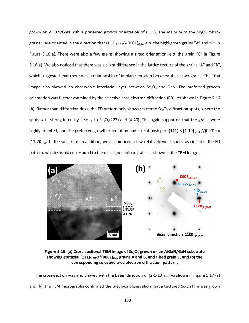
130
grown on AlGaN/GaN with a preferred growth orientation of (111). The majority of the Sc2O3 micro-
grains were oriented in the direction that (111)Sc2O3//(0001)GaN, e.g. the highlighted grains “A” and “B” in
Figure 5.16(a). There were also a few grains showing a tilted orientation, e.g. the grain “C” in Figure
5.16(a). We also noticed that there was a slight difference in the lattice texture of the grains “A” and “B”,
which suggested that there was a relationship of in-plane rotation between these two grains. The TEM
image also showed no observable interfacial layer between Sc2O3 and GaN. The preferred growth
orientation was further examined by the selective area electron diffraction (ED). As shown in Figure 5.16
(b). Rather than diffraction rings, the ED pattern only shows scattered Sc2O3 diffraction spots, where the
spots with strong intensity belong to Sc2O3(222) and (4-40). This again supported that the grains were
highly oriented, and the preferred growth orientation had a relationship of (111) × [1-10]Sc2O3//(0001) ×
[11-20]GaN to the substrate. In addition, we also noticed a few relatively weak spots, as circled in the ED
pattern, which should correspond to the misaligned micro-grains as shown in the TEM image.
Figure 5.16. (a) Cross-sectional TEM image of Sc2O3 grown on an AlGaN/GaN substrate showing epitaxial (111)Sc2O3//(0001)GaN grains A and B, and tilted grain C, and (b) the
corresponding selective area electron diffraction pattern.
The cross-section was also viewed with the beam direction of [2-1-10]GaN. As shown in Figure 5.17 (a)
and (b), the TEM micrographs confirmed the previous observation that a textured Sc2O3 film was grown

131
on AlGaN/GaN. Moreover, the corresponding selective area electron diffraction pattern (Figure 5.17 (c))
also revealed an in-plane 180˚ twin relationship of Sc2O3 grains, since there are two sets of major
diffraction patterns (labeled by purple and green arrows in Figure 5.17 (c)). This twin relation is due to
the degenerate growth of an fcc structure on a hexagonal (0001) surface, since the fcc can grow either
following ABCABC… or ACBACB… stacking orders.
Figure 5.17. (a and b) Cross-sectional TEM images of Sc2O3 grown on an AlGaN/GaN substrate. (The embedded 1 nm AlN layer was clearly observed in (b).) (c) The
corresponding selective area electron diffraction pattern, where two sets of Sc2O3 diffraction patterns were labeled by purple and green arrows, respectively.

132
X-ray diffraction (XRD) measurements were also performed on the Sc2O3/AlGaN/GaN sample. As
shown in Figure 5.18, the high-resolution XRD (HRXRD) scan only showed GaN (0002) and AlGaN (0002)
peaks, but it did not show the Sc2O3 (222) peak at the 2θ angle of 31.45˚, which suggested that the Sc2O3
film was not an epitaxial film.
Figure 5.18. High-resolution XRD scan of a 21 nm Sc2O3 film grown on an AlGaN/GaN substrate. Only GaN (0002) and AlGaN (0002) peaks were observed, but not the Sc2O3
(222) peak (2θ = 31.45˚), suggesting the Sc2O3 film was not an epitaxial film.
The Sc2O3/AlGaN/GaN sample was also examined by 2-dimensional XRD (2DXRD). Two 2DXRD scans
around GaN (0002) were performed. The sample was intentionally placed off from the symmetric
configuration, i.e. ω ≠ θ, to avoid the strong reflection from the single crystal substrate. A diffraction
pattern of the sample with ω = 16˚ is shown in Figure 5.19(a), and another diffraction pattern with an
additional sample rotation of φ = 10˚ is shown in Figure 5.19(b). The corresponding integrated spectra
are shown in Figure 5.19(c) and (d), respectively. (See Figure 3.4 for the definitions of ω, θ and φ.)
Assuming the film is polycrystalline or textured, a φ rotation should not affect the peak intensity from
the film, but it would greatly diminish the peak intensity from the single crystal substrate. The 2DXRD

133
patterns clearly indicated that the Sc2O3 film was highly textured, as only sharp spots, instead of rings,
were shown in the patterns. The measured 2θ angles of GaN (0002) and Sc2O3 (222) were well matched
with those of the bulk materials. Especially, the double-dot pattern of Sc2O3 (222) reflection in Figure
5.19(a) is similar as the double-dot pattern in the electron diffraction pattern (Figure 5.17(c)). Combining
the results of HRXRD and 2DXRD, we conclude again that our ALD Sc2O3 film grown on AlGaN/GaN
substrate has a highly textured crystalline structure.
Figure 5.19. 2-dimensional XRD (2DXRD) of the same Sc2O3/AlGaN/GaN sample as in Figure 5.18. (a) and (b) show the two 2DXRD scans without and with a sample rotation (φ). (c) and (d) are the corresponding integrated spectra. The 2θ angles of GaN (0002)
and Sc2O3 (222) are 34.56˚ and 31.45˚, respectively. The star (*) in (c) denotes an artifact peak due to the single crystal substrate.

134
The surface morphology of the Sc2O3/AlGaN/GaN sample was evaluated by AFM. As shown in Figure
5.20, the rms roughness was measured to be 0.82 nm, which was consistent with the cross-sectional
TEM observations.
Figure 5.20. AFM of the same Sc2O3/AlGaN/GaN sample as in Figure 5.18. The rms roughness was 0.82 nm.
Sc2O3 was deposited on AlGaN/GaN HEMT device structures for characterizing the electrical
properties. Both of the device fabrication and electrical characterization were performed by Omair I.
Saadat in Prof. Tomás Palacios’ group at MIT. The HEMT devices were fabricated on the same
AlGaN/GaN substrates as for the structural analysis above. Ti/Al/Ni/Au ohmic metals were patterned,
deposited and annealed at 870˚C to form ohmic source/drain contacts. Then, mesa isolation was
performed by etching with a Cl2/BCl3 plasma before deposition of the gate dielectric. In order to study
the effect of surface treatment before the Sc2O3 deposition, some of the devices samples were first
exposed to UV in air for 5 minutes, and then immersed in NH4OH (aqueous, 15%) for 10 minutes, while
some other samples were only treated with UV. Then 21 nm of Sc2O3 was deposited on top of the device
samples at the temperature of 330 ˚C by 400 ALD cycles. After the Sc2O3 deposition, Ni/Au/Ni gates were
deposited by e-beam evaporation and patterned by liftoff. The schematic view of the Sc2O3/AlGaN/GaN
device structure is illustrated in Figure 5.21.
1.0
0.8
0.6
0.4
0.2
0.0
µm
1.00.80.60.40.20.0
µm
-2
-1
0
1
2
nm

135
Figure 5.21. Schematic view of the Sc2O3/AlGaN/GaN device structure.
Both the UV treated and NH4OH treated Sc2O3/AlGaN/GaN HEMTs show excellent Ion/Ioff
characteristics as shown in Figure 5.22. Transfer characteristics show an excellent Ion/Ioff ratio of over 108
with a subthreshold slope of 75 mV/dec for the HEMTs with the NH4OH treatment. To avoid any
complication with the physisorbed moisture on Sc2O3, these electrical measurements were performed
under vacuum. This effect can be minimized by adding another moisture blocking layer like Al2O3 or
Teflon.35 The Sc2O3 dielectric layer is also effective in helping to deplete carriers in the channel, which is
necessary for enhancement-mode operation. The bare AlGaN/GaN HEMT has a carrier concentration of
6.5 × 1012 cm-2 but the samples with Sc2O3 have a carrier concentration of 5 × 1012 cm-2. Coupled with
the excellent subthreshold slope, Sc2O3 based oxides are very promising for AlGaN/GaN HEMTs for
power applications.
Figure 5.22. Transfer characteristics of HEMTS show excellent Ion/Ioff ratios.
-5 -4 -3 -2 -1 0 110
-8
10-6
10-4
10-2
100
102
104
Vgs
(V)
I ds (
mA
/mm
)
UV
NH4OH

136
5.4 Pulsed CVD of ScN
ScN itself is unlikely to be a good passivation layer for AlGaN/GaN devices, since its band gap is fairly
low (2.1 ~ 3.2 eV).36 However, ScN has been found to be useful for growing low-dislocation GaN single
crystal films.37, 38 In addition, thin films of scandium aluminum nitride alloy (ScxAl1-xN) have been
demonstrated to exhibit a good piezoelectric response at a fairly high working temperature.39-41
Figure 5.23. (a and b) TEM images of a “ScN” film deposited on a SiNx TEM grid. The corresponding electron diffraction pattern (c) indicated the crystalline grains in (a) and
(b) were actually Sc2O3, suggesting the film was readily oxidized by the air.
Our preliminary experiments showed that the Sc precursor (as used for the Sc2O3 deposition in
Section 5.3), scandium tris(N,N’-diisopropylacetamidinate), also produced ScN films when using NH3 as
the co-reactant gas. The deposition was performed in a pulsed CVD mode with NH3 (1 Torr) at 330 ˚C.
Figure 5.23 shows the TEM results of a film deposited from 500 pulses of the Sc precursor. The TEM
micrographs showed crystalline features with smaller grain size compared to Sc2O3. However, these
crystalline grains were determined to be Sc2O3, rather than ScN, based on the electron diffraction
pattern as shown in Figure 5.23(c). We believe this is because our as-deposited ScN film was amorphous
with a low density so that it was readily oxidized by the air. In the future, one may consider running the
ScN deposition at an even higher temperature, aiming for better crystallized films, since single

137
crystalline ScN is fairly stable against oxidation.42 One may also consider depositing an in-situ capping
layer on the amorphous ScN films to prevent the films from oxidation.
5.5 Other oxides for GaN-based HEMT devices
We have also tried LaAlO3 and La2O3 as the high-k dielectrics for GaN-based HEMT devices. Both
LaAlO3 and La2O3 were deposited at 300 ˚C, using the ALD processes described in Chapter 4 of this thesis.
The as-deposited LaAlO3 films were amorphous and the as-deposited La2O3 films were polycrystalline.
The test structure of the HEMT devices is schematically shown in Figure 5.24. The structure is generally
similar as the test structure for Sc2O3 (Figure 5.21). But in this work, a 20 nm layer of LaAlO3 or La2O3 was
used as the gate dielectric instead of Sc2O3, and the bottom AlGaN/GaN layer was grown on a Si (111)
substrate, consisting of a 1 μm AlN buffer layer grown on Si, followed by 1 μm GaN, and 25 nm AlGaN
(25% Al) on top. Due to the large lattice mismatch between Si and GaN, the epitaxial GaN layer had a
large density of threading dislocations (109 ~ 1010 cm-2) throughout the entire layer stack as shown in the
cross-sectional TEM images (Figure 5.25).
Figure 5.24. Schematic diagram of the HEMT device structure for evaluating the electrical properties of the dielectric oxides.

138
Figure 5.25. Cross-sectional TEM images of sample of AlGaN/GaN on Si (111). Due to the large lattice mismatch between Si and GaN, the GaN layer had a high density of
dislocations.
The measurements of the HEMT device properties were performed by Omair I. Saadat in Prof. Tomás
Palacios’ group at MIT. The preliminary tests showed that the ALD LaAlO3 withstood a 10 V gate bias,
whereas all the other oxides tested, including La2O3, Sc2O3, and HfO2, broke down at 10 V gate bias. This
is likely due to the amorphous feature of the ALD LaAlO3. Therefore, ALD LaAlO3 is a promising gate
dielectric for power device applications.
The C-V dispersion results are shown in Figure 5.26. Comparatively, La2O3 showed fairly small
frequency dispersion of at Vbias ~ -5 V (Figure 5.26 (b)), suggesting that there was very little trapping at
the transition between the depletion and accumulation regions. La2O3 also showed smaller dispersion at
high bias region (Vbias > 2 V), compared to LaAlO3 (Figure 5.26 (a)). We also integrated the capacitance
over Vbias, and obtained the curves of charge density versus Vbias (Figure 5.26 (c) and (d)), where the
difference between the 100 Hz and 1MHz curves is the minimum trap density for the oxide. The
minimum trap densities for LaAlO3 and La2O3 were estimated to be 1 × 10¹³ traps/cm2 and 3 × 10¹²
traps/cm2, respectively. Therefore, La2O3 might be a promising passivation layer for GaN-based HEMT
devices.

139
Figure 5.26. C-V frequency dispersion results of (a) LaAlO3 and (b) La2O3. (c) and (d) showed the corresponding integrated charge density versus Vbias curves.
In summary, as LaAlO3 could withstand a high bias and La2O3 had a small trap density, a combination
of La2O3 surface passivation and LaAlO3 gate dielectric seemed promising for GaN-based HEMT
applications. Further tests on high-quality GaN substrates are needed to draw solid conclusions, since
the current results of the device properties might be affected by the high density of dislocation in the
GaN substrates (Figure 5.25).
140
5.6 References
1 R. C. Fitch, et al., J. Vac. Sci. Technol. B 29 (2011).
2 Z. H. Liu, G. I. Ng, H. Zhou, S. Arulkumaran, and Y. K. T. Maung, Appl. Phys. Lett. 98 (2011).
3 S. Huang, Q. M. Jiang, S. Yang, C. H. Zhou, and K. J. Chen, IEEE Electron Device Lett. 33, 516
(2012).
4 A. M. Herrero, B. P. Gila, C. R. Abernathy, S. J. Pearton, V. Craciun, K. Siebein, and F. Ren, Appl.
Phys. Lett. 89 (2006).
5 S. J. Pearton, C. R. Abernathy, F. Ren, and Gallium nitride processing for electronics, sensors and
spintronics (Springer-Verlag, 2006).
6 M. Alevli, C. Ozgit, I. Donmez, and N. Biyikli, Physica Status Solidi a-Applications and Materials
Science 209, 266 (2012).
7 J. Dendooven, D. Deduytsche, J. Musschoot, R. L. Vanmeirhaeghe, and C. Detavernier, J.
Electrochem. Soc. 157, G111 (2010).
8 M. Bosund, T. Sajavaara, M. Laitinen, T. Huhtio, M. Putkonen, V. M. Airaksinen, and H. Lipsanen,
Appl. Surf. Sci. 257, 7827 (2011).
9 X. Y. Liu, S. Ramanathan, E. Lee, and T. E. Seidel, in Integration of Advanced Micro-and
Nanoelectronic Devices-Critical Issues and Solutions, edited by J. Morais, D. Kumar, M. Houssa, R. K.
Singh, D. Landheer, R. Ramesh, R. M. Wallace, S. Guha and H. Koinuma (Materials Research Society,
Warrendale, 2004), Vol. 811, p. 11.
10 K. H. Kim, N. W. Kwak, and S. H. Lee, Electron. Mater. Lett. 5, 83 (2009).
11 R. G. Gordon, D. M. Hoffman, and U. Riaz, J. Mater. Res. 6, 5 (1991).
12 R. G. Gordon, U. Riaz, and D. M. Hoffman, J. Mater. Res. 7, 1679 (1992).
13 H. Cho, K. P. Lee, B. P. Gila, C. R. Abernathy, S. J. Pearton, and F. Ren, Electrochem. Solid State
Lett. 6, G119 (2003).

141
14 Y. Irokawa, et al., Appl. Phys. Lett. 84, 2919 (2004).
15 J. Kim, R. Mehandru, B. Luo, F. Ren, B. P. Gila, A. H. Onstine, C. R. Abernathy, S. J. Pearton, and Y.
Irokawa, Appl. Phys. Lett. 80, 4555 (2002).
16 R. Huang and A. H. Kitai, Appl. Phys. Lett. 61, 1450 (1992).
17 R. Huang and A. H. Kitai, Journal of Electronic Materials 22, 215 (1993).
18 R. Huang and A. H. Kitai, Journal of Materials Science Letters 12, 1444 (1993).
19 M. Putkonen, T. Sajavaara, and L. Niinisto, J. Mater. Chem. 10, 1857 (2000).
20 B. B. Burton, D. N. Goldstein, and S. M. George, J. Phys. Chem. C 113, 1939 (2009).
21 M. Putkonen, L. S. Johansson, E. Rauhala, and L. Niinisto, J. Mater. Chem. 9, 2449 (1999).
22 T. Hatanpaa, J. Ihanus, J. Kansikas, I. Mutikainen, M. Ritala, and M. Leskela, Chem. Mat. 11, 1846
(1999).
23 Y. Kuroda, E. Yasugi, H. Aoi, K. Miura, and T. Morimoto, Journal of the Chemical Society-Faraday
Transactions I 84, 2421 (1988).
24 K. Refson, R. A. Wogelius, D. G. Eraser, M. C. Payne, M. H. Lee, and V. Milman, Physical Review B
52, 10823 (1995).
25 R. Mehandru, et al., Appl. Phys. Lett. 82, 2530 (2003).
26 A. Y. Polyakov, et al., Appl. Phys. Lett. 83, 2608 (2003).
27 J. J. Chen, B. P. Gila, M. Hlad, A. Gerger, F. Ren, C. R. Abernathy, and S. J. Pearton, Appl. Phys.
Lett. 88 (2006).
28 J. S. Jur, V. D. Wheeler, D. J. Lichtenwalner, J. P. Maria, and M. A. L. Johnson, Appl. Phys. Lett. 98
(2011).
29 X. Weng, W. Tian, D. G. Schlom, and E. C. Dickey, Appl. Phys. Lett. 96 (2010).
30 W. M. M. Kessels and M. Putkonen, Mrs Bulletin 36, 907 (2011).

142
31 P. de Rouffignac, A. P. Yousef, K. H. Kim, and R. G. Gordon, Electrochem. Solid State Lett. 9, F45
(2006).
32 M. Hong, et al., Appl. Phys. Lett. 87 (2005).
33 M. M. Frank, Y. J. Chabal, and G. D. Wilk, Appl. Phys. Lett. 82, 4758 (2003).
34 Y. Liu, M. Xu, J. Heo, P. D. Ye, and R. G. Gordon, Appl. Phys. Lett. 97 (2010).
35 F. C. Gao, D; Lu, B; Tuller, H. L.; Thompson, C.V.; Keller, S; Mishra, U. K.; Palacios, T., Electron
Device Letters (To be published).
36 M. A. Moram, Z. H. Barber, and C. J. Humphreys, Thin Solid Films 516, 8569 (2008).
37 M. A. Moram, C. F. Johnston, M. J. Kappers, and C. J. Humphreys, J. Cryst. Growth 311, 3239
(2009).
38 M. A. Moram, Y. Zhang, M. J. Kappers, Z. H. Barber, and C. J. Humphreys, Appl. Phys. Lett. 91
(2007).
39 M. Akiyama, T. Kamohara, K. Kano, A. Teshigahara, Y. Takeuchi, and N. Kawahara, Adv. Mater.
21, 593 (2009).
40 M. Akiyama, K. Kano, and A. Teshigahara, Appl. Phys. Lett. 95 (2009).
41 M. Akiyama, T. Tabaru, K. Nishikubo, A. Teshigahara, and K. Kano, Journal of the Ceramic Society
of Japan 118, 1166 (2010).
42 R. Niewa, D. A. Zherebtsov, M. Kirchner, M. Schmidt, and W. Schnelle, Chem. Mat. 16, 5445
(2004).

143
Chapter 6 Selective Silica Coating for Dye-sensitized
Solar Cells
6.1 Introduction
Dye-sensitized solar cells (DSCs) have great potential to compete with conventional p−n junction
solar cells due to their relatively low-cost.1-6 However, their efficiency is limited by the ease with which
electrons collected by the nanoparticle framework can recombine with ions in solution. Therefore, the
photovoltaic efficiency of DSCs can be increased by retarding electron recombination at the
photoelectrode interfaces. The surfaces of the TiO2 nanoparticles are not fully covered by the dye
molecules as shown schematically in Figure 6.1. Thus an electrical short by direct contact between
electrolyte and the areas of TiO2 not covered by dye provides an important loss pathway by which
electrons recombine with the electrolyte. This recombination rate could be reduced or eliminated by
selectively coating an insulating and transparent layer on these open areas of TiO2. In an effort to
minimize such losses, many groups have proposed device architectures that include the coating of
inorganic barrier layers,7, 8 the use of long aliphatic chain on organic framework,9, 10 saccharides,11 the
introduction of co-adsorbents,12-14 encapsulation by cyclodextrins,15 and post-surface passivation by
polymerization.16, 17 Recently high band gap metal oxide layers prepared via atomic layer deposition
(ALD) have received much attention as efficient interface engineering tools owing to their capability of
infiltrating porous structures, thereby ensuring good coverage of the surface of the nanoporous
electrode,18, 19 fine control of thickness,20, 21 and low-temperature processing.22, 23 However, applying ALD
layers prior to dye adsorption on TiO2 or related oxides significantly reduces the electron-transfer rate
from the dye through the metal oxide overlayers by creating a tunneling barrier.24-27 Therefore, a new
methodology is needed that does not interfere with electron transfer to or from the dye molecules.

144
Figure 6.1. Post-dye SiO2 deposition process and plausible reaction mechanism on dye-
coated TiO2 nanoparticles.
We discovered a method to deposit selectively an insulating and transparent layer of silica (SiO2) only
on the open areas of TiO2 surface, but not on the adsorbed dye molecules or between the dye surface-
linker and the electrode. Our approach exploits deposition of SiO2 from a precursor that is catalytically

145
decomposed by the surface of TiO2. Areas of TiO2 covered by adsorbed dye do not catalyze the
deposition of SiO2. Thus the gaps between dye molecules are selectively covered by SiO2. This SiO2
retards the interfacial charge recombination dynamics without hindering electron injection from the dye
into the TiO2 or from the solution into the dye. When this SiO2 treatment was applied to a DSC just after
coating the TiO2 with an organic dye (OrgD, Figure 6.1), enhanced performance was obtained, with a
higher power conversion efficiency and longer electron lifetime. Another important feature of the SiO2
deposition process is that its thickness is self-limiting, so the same thickness is applied to all levels in the
porous multilayer structure of the photoelectrode. In this study, we investigated the conditions needed
to make SiO2 deposit selectively on TiO2 between dyes.
We found that silica less than 1 nanometer thick functions as a barrier to charge recombination and
thereby improves the performance of these photovoltaic devices. The SiO2 coating chemistry is related
to a process for rapid ALD using alternating exposure of surfaces to vapors of trimethylaluminum (TMA)
as a catalyst and tris(tert-butoxy)silanol (TBOS) as the SiO2 precursor.28 In this reaction, aluminum placed
on the surface by the TMA plays a crucial role as a Lewis-acidic catalyst for deposition of SiO2 layers up
to 15 nm thick on top of the alumina.29 There have been reports that hafnium and zirconium can also
catalyze the growth of SiO2.30-33 This work suggested to us that titanium might also catalyze the growth
of SiO2. Indeed, we have found that anatase titanium dioxide does, in fact, catalyze growth of SiO2 on its
surface.
6.2 Experimental
Preparation of OrgD-containing photoanodes: The dye-loaded photoanodes were prepared by Dr.
Ho-Jin Son in Prof. Joseph T. Hupp’s group at Northwestern University. The organic dye (OrgD) was
synthesized and purified as published.34 Fluorine-doped tin oxide (FTO) coated glass plates (Hartford
Glass, TEC 15) were immersed in 40 mM TiCl4 (aqueous) at 70 °C for 30 min and washed by water and

146
ethanol. A transparent TiO2 layer on the FTO glass plate was prepared by doctor blade printing
commercially available TiO2 paste (ave. 20 nm, Dyesol, DSL-90-T), and then dried for 2h at 25 °C. The
TiO2 electrodes were gradually heated under flowing air at 325 °C for 15 min, at 375 °C for 15 min, at
450 °C for 15 min, and at 500 °C for 15 min. l A paste containing 400 nm diameter particles (WER4-0,
Dyesol) for the scattering layer was deposited by doctor blade printing and then dried for 2 h at 25 °C.
The TiO2 electrodes were gradually heated under flowing air at 325 °C for 15 min, at 375 °C for 15 min,
at 450 °C for 15 min, and at 500 °C for 15 min. The resulting layer was composed of 12 μm thickness of
transparent layer and 6 μm thickness of scattering layer. The active section of the photoelectrode was
then geometrically defined by using a razor blade to remove material that would fall outside of the
intended illumination area. This step eliminates artifacts (overly large photocurrents) due to light
leakage onto portions of the electrode that not intentionally illuminated. The photoelectrodes were
treated again with TiCl4 at 70 °C for 30 min and sintered at 500 °C for 30 min. Dye adsorption was
accomplished by soaking the TiO2 films in a 0.3 mM solution of OrgD. After 12 h, the films were washed
with copious amount of the above solvent and dried with a nitrogen stream.
Silica coating: The dye-loaded photoanode (FTO/TiO2/dye) was sealed in a vacuum food package,
and transferred to our lab for SiO2 coating. The SiO2 coating was performed in a home-built hot-wall
tubular reactor. Tris(tert-butoxy)silanol was used as the precursor for both the silicon and the oxygen.
The molten silanol was held in a glass bubbler inside an oven at 100 °C. The reactor tube was first
pumped down to about 10-2 Torr pressure. Then a valve was opened for 1 second to deliver silanol vapor
at a pressure of about 1 Torr, and then the reactor tube was isolated for 5 minutes to allow the reaction
l In the case of preparing N719 dye-containing photoanodes, which were used to compare the
photovoltaic properties with OrgD, home-made TiO2 paste with smaller size (~10 nm) was used to make the transparent TiO2 layer. This is because N719 has a relatively low extinction coefficient (14,000 M-1
cm-1) as compared to OrgD (43,500 M-1 cm-1). Therefore, N719 needs a much thicker TiO2 layer to achieve comparable light harvesting efficiency (LHE). However, thicker TiO2 layer made from commercial TiO2 paste (~20nm) had severe peeling and cracking issues after annealing.
147
to go to completion. The reaction temperature was varied from 130 °C to 190 °C, since no SiO2 film was
deposited below 130 °C, and the dye molecules may be unstable or agglomerate above 190 °C. Once the
silica deposition was completed, the partially-completed solar cells were cooled in pure nitrogen to near
room temperature before their removal from the deposition chamber. The solar cells were kept in a
food vacuum package after the SiO2 deposition until the remainder of the cell construction was
completed by adding the electrolyte and the back contact. This handling procedure protected the dye
from contamination and/or oxidation by the ambient air.
In order to determine the amount of SiO2 deposited, planar samples of anatase TiO2 ~ 20 nm thick
were deposited on UV-ozone-treated glassy carbon substrates. These TiO2 layers were grown by 750
cycles of ALD from titanium isopropoxide vapor alternating with water vapor at a substrate temperature
of 225 °C. The as-deposited TiO2 was in polycrystalline anatase phase. The mass per unit area of SiO2 was
measured by Rutherford backscattering spectrometry (RBS)m on these planar TiO2 samples, and
converted to thicknesses assuming that the SiO2 has the bulk density of 2.0 g/cm3. The distribution of
SiO2 coating through the TiO2 nanoparticle layers was examined by energy dispersive X-ray spectroscopy
(EDS, EDAX, Apollo 40) in a scanning electron microscope (SEM, Zeiss, supra55VP), operated at an
acceleration voltage of 6 keV.
Assembly of photovoltaic cells: Cathode/anode pairs were combined in each case with a 60-μm-thick
Surlyn polymer film (Surlyn-1702, Dupont) that served as a spacer and defined the perimeter of a
photoelectrochemical sealing. The components were permanently combined by placing them on a
hotplate at 90 °C and allowing the spacer to melt slightly. Tin-coated copper wires were connected to
each electrode with silver epoxy. 0.60 M 1,2-dimethyl-3-propylimidazolium iodide (98%, TCI), 0.05 M I2
(99.8%, Aldrich), and 0.50 M 4-tert-butylpyridine (99%, Aldrich) in acetonitrile (99.5%, Aldrich)
m RBS measurements were obtained using 2 MeV He++ ions on a 1.7 MV tandem accelerator at
Rutgers University.

148
constituted the cell solvent, redox electrolyte, and inert electrolyte. For N719 cells, the electrolyte
consisted of 0.60 M 1-methyl-3-butyl imidazolium iodide (98%, TCI), 0.03 M I2 (99.8%, Aldrich), 0.10 M
guanidinium thiocyanate, and 0.50 M 4-tert-butylpyridine (99%, Aldrich) in acetonitrile:valeronitrile
(85:15). ~ 30 μL of electrolyte-containing solution was dropcast onto the drilled hole on the back side of
the platinized cathode and then vacuum-loaded into the cell. After residual electrolyte around the hole
was removed, the hole was sealed by melting a sheet of Surlyn polymer film that was inserted between
the backside of the FTO and a micro cover glass slide. Finally, a photo-mask (black tape) as an aperture
was applied on top of the active area of each cell. For discussions of the cell fabrication, see reports by
G.-W. Lee, et al.35 and S. Ito, et al. 36
Spectroscopic and electrical measurements: UV-Vis spectra of samples were recorded on a Varian
Cary 5000 UV-VIS-NIR spectrophotometer. The photocurrent-density-to-applied-voltage (J−V) curves
and IPCE curves of photovoltaic cells were obtained using a home-made setup which consists of a xenon
lamp, an AM 1.5 light filter, and a CHI 1202 Electrochemical Analyzer (CHI instruments). The power of
filtered light was calibrated by an optical power meter (OPM) and adjusted to 100 mW/cm2.
6.3 Results and discussion
The SiO2 coating process was performed in a home-built hot-wall tubular reactor (Figure 6.1). TBOS
was used as the precursor for both the silicon and the oxygen. The thickness of SiO2 deposited on planar
witness samples of TiO2 is plotted as a function of substrate temperature in Figure 6.2. The reaction
temperature was varied from 130 °C to 190 °C, since no SiO2 film was deposited below 130 °C. The
amount of SiO2 deposited was measured by the Rutherford Backscattering Spectroscopy (RBS) technique.
The thickness of the SiO2 film was found to increase with temperature from 0.8 nm to about 1.2 nm.
These thicknesses represent the self-limited values obtained after initial dosing of about 1 torr of silanol
vapor, which was then allowed to react for 5 minutes. Other experiments showed that almost all of this

149
deposition occurs within the first 10 seconds. Energy-dispersive X-ray spectroscopic (EDS) analyses
(Figure 6.2) showed that the SiO2 is evenly distributed throughout the thousands of TiO2 nano-particle
(NP) layers constituting the photoanode. The coverage and thickness of the SiO2 layer on the TiO2 NPs
were further examined with HRTEM (see Figure 6.3), which also shows a uniform and conformal SiO2
layer. The thickness of the SiO2 layer was ~ 1 nm and ~ 3 nm for 140 and 250 °C, respectively, showing
the temperature-dependence of the thickness, consistent with thicknesses determined by RBS.
Figure 6.2. (a) RBS data for the thickness of the SiO2 layer as a function of deposition temperature. (b) EDS data showing that the SiO2 is deposited uniformly throughout
the porous, nanoparticulate TiO2 electrode.
Although it is not ideal to compare the thickness of SiO2 on the dye-loaded TiO2 surface with that on
a flat surface, it should be noted that the real thickness of SiO2 deposited is similar to the vertical
dimension of dye molecules as evidenced by the stable oxidation of dyes within TiO2/SiO2 films (Figure
6.4) and the corresponding I−V performance studied below (see Table 6.1). (Thicker layers might shut-
off dye electrochemistry.) In UV/vis spectra of TiO2/OrgD/SiO2 films, no significant decrease in
absorbance is observed after SiO2 deposition, indicating the sensitizing dye molecules are not affected
by the SiO2 precursor or the thermal stress during SiO2 deposition (Figure 6.5 and Figure 6.6). Given the
fact that the sensitized dye molecules are partly surrounded by the SiO2 layer, resulting in a change of
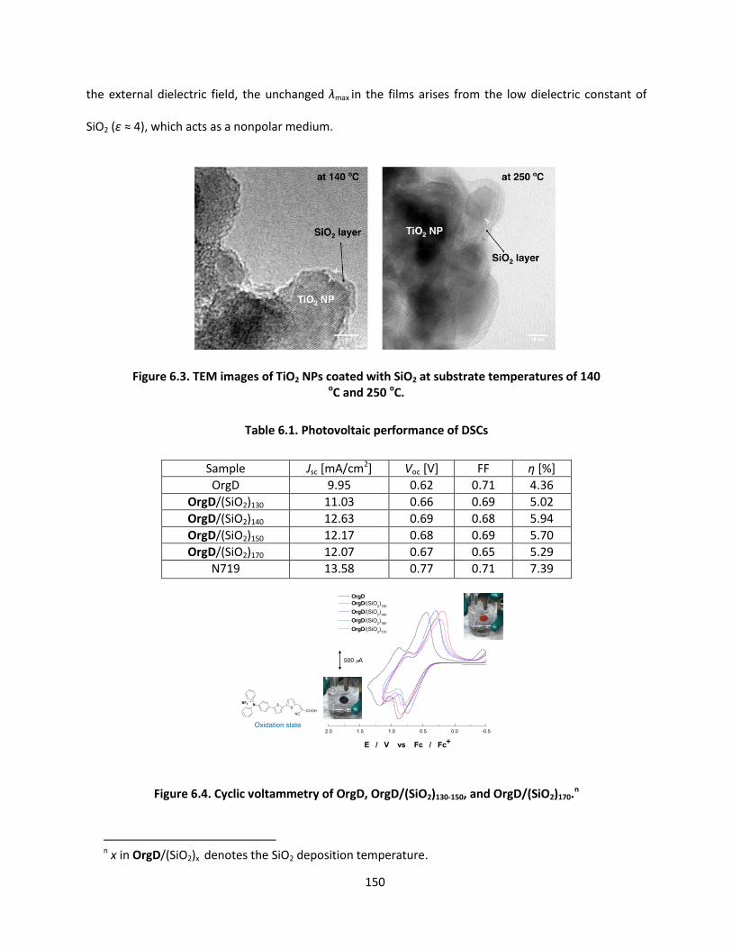
150
the external dielectric field, the unchanged λmax in the films arises from the low dielectric constant of
SiO2 (ε ≈ 4), which acts as a nonpolar medium.
Figure 6.3. TEM images of TiO2 NPs coated with SiO2 at substrate temperatures of 140 oC and 250 oC.
Table 6.1. Photovoltaic performance of DSCs
Sample Jsc [mA/cm2] Voc [V] FF η [%]
OrgD 9.95 0.62 0.71 4.36
OrgD/(SiO2)130 11.03 0.66 0.69 5.02
OrgD/(SiO2)140 12.63 0.69 0.68 5.94
OrgD/(SiO2)150 12.17 0.68 0.69 5.70
OrgD/(SiO2)170 12.07 0.67 0.65 5.29
N719 13.58 0.77 0.71 7.39
Figure 6.4. Cyclic voltammetry of OrgD, OrgD/(SiO2)130-150, and OrgD/(SiO2)170.n
n x in OrgD/(SiO2)x denotes the SiO2 deposition temperature.

151
Figure 6.5. UV/vis spectra of TiO2/OrgD coated with SiO2 at temperatures from 130 to 170 oC, compared with a control electrode without SiO2.
Figure 6.6. J-V curves of DSCs containing TiO2/OrgD photoelectrodes subjected to no heating (RT) or heating at 150 or 200 oC.
Enshrouding dyes with a glass (SiO2) coating of precise and uniform thickness substantially improves
the photovoltaic performance of the DSC devices. Figure 6.7 shows action spectra in the form of
monochromatic incident photon-to-current conversion efficiencies (IPCEs) for DSCs based on OrgD
(electrolyte: 0.6 M DMPImI, 0.05 M iodine, 0.1 M LiI, and 0.5 M tert-butylpyridine in acetonitrile). The
post-dye-treated OrgD/(SiO2)x (x = SiO2 deposition temperature ranging from 130 to 170 °C) cells clearly
exhibited an increased response over the entire spectral region, but especially the red region, relative to
the nontreated OrgD cell. The IPCE of OrgD/(SiO2)130-170 showed plateaus of over 75% from 400 to 590

152
nm. Significantly higher responses were observed over the wavelength range of 500-700 nm for
OrgD/(SiO2)130-170 cells compared to OrgD cell. The broadened IPCEs of these coated cells suggest
superior electron collection capability (greater collection length) versus untreated cells. If we examine
IPCEs as a function of light harvesting efficiency over the wavelength (Figure 6.8), the results suggest
that the coated films have much longer effective light infiltration compared to uncoated ones (“effective”
means ability to inject electrons that are subsequently collected as a photocurrent rather than lost to
interception by I3- or recombination with oxidized dye). An additional minor contributor to the IPCE
broadening could be a red shift in dye absorption following encapsulation. Extinction measurements
suggest that, depending on the wavelength, the shift could be as large as 15 nm. The measurements
were complicated, however, by baseline shifts presumably due to light scattering.
Figure 6.7. J−V curves, dark currents, and IPCE plots (inset) of OrgD (black dashed line), OrgD/(SiO2)140 (red line), and OrgD/(SiO2)150 (blue line).

153
Figure 6.8. Light harvesting efficiency (LHE) for (a) OrgD and (b) OrgD/(SiO2)140 on TiO2 films of various thickness (10 and 20 μm). LHE plots were calculated from absorption data using 12 μm thick films, by assuming that absorbances scale directly with film
thickness.o Also shown are the IPCE plots for cells containing (a) OrgD and (b) OrgD/(SiO2)140 on photoelectrodes featuring 12 μm of nanoparticulate TiO2 and 6 μm of 400 nm diameter TiO2 particles for light scattering. Notice that the IPCE lineshape
without silica treatment resembles the LHE plot corresponding to a thin film, while the IPCE lineshape with silica treatment resembles LHE plots corresponding to much
thicker films. For reasons that are not clear, but perhaps associated with residual light scattering, absorption spectra for nominally identical films were shifted by a few to
several nanometers with respect to each other. Consequently, not too much significance should be attached to matching red LHE edges with the red IPCE edge.
Instead the shapes of the IPCE and LHE plots should be compared. Since the films used for IPCE measurements include a thick scattering layer, which should behave as a good
mirror, photons that pass through the 12 μm nanoparticulate portion of the photoelectrode unabsorbed have the opportunity to be absorbed on the reflective
pass-through. Thus, a 12 μm photoelectrode could, in the absence of significant charge recombination, behave in an IPCE measurement as if it were ~20 μm thick.
The photovoltaic performances of the OrgD sensitized cells are listed in Table 6.1. The optimal
condition for the SiO2 barrier was that produced at 140 °C (~ 1.0 nm by RBS), which resulted in 36%
increase in efficiency (η) compared to the reference cell, with the highest η achieved being 5.94%; both
the open-circuit photovoltage (Voc) value of 0.69 V and the short-circuit photocurrent (Jsc) value of 12.63
o In other words, all LHE curves were calculated by starting with absorbance values for OrgD, withour or with
SiO2 treatment, from 12 μm thick films. Reflection by FTO and scattering by 400 nm particles are not taken into account.

154
mA/cm2 are larger than for the uncoated control.p This value agrees well with that obtained by
integrating solar-spectrum-weighted IPCE. Under the same conditions, the OrgD cell gave Jsc = 9.95
mA/cm2, Voc = 0.62 V, and fill-factor (ff) = 0.71, which correspond to η = 4.36%. When the deposition
temperature was increased to 150 °C, the resulting device showed slightly poorer characteristics than
the OrgD/(SiO2)140 cell. Of particular importance is the 60-70 mV increase in the Voc value of the
OrgD/(SiO2)130-170 cell relative to the OrgD cell. This result implies that the SiO2 surrounding the dye
results in retardation of interfacial charge recombination losses in the device, as confirmed by the dark
current data (Figure 6.7). Charge lifetimes (τe) determined from Voc decay measurements are shown in
Figure 6.9(a). The τe values are successively shifted to larger values with increase of reaction
temperature from 130 to 170 °C, demonstrating that the electron-recombination process was effectively
retarded by the SiO2 deposition. Specifically, the increase of τe by the post-dye SiO2 layer is saturated
with the amount produced at 140 °C, showing that as little as 1.0 nm of SiO2 (about 4 monolayers) is
sufficient to insulate the TiO2 surfaces very efficiently. These results are also in good agreement with the
Voc results shown in Table 6.1.
Electrochemical impedance spectroscopy (EIS) was performed under dark conditions (Figure 6.9(b))
with the forward bias ranging from −0.5 V to −0.7 V. The semicircular curve obtained in the
intermediate-frequency regime shows the dark reaction impedance caused by electron transport from
the TiO2 conduction band to the I3− ions in the electrolyte.37 The radius of the intermediate frequency
semicircle showed the increasing order of OrgD (72 Ω) < OrgD/(SiO2)130 (133 Ω) < OrgD/(SiO2)140 (239 Ω)
≤ OrgD/(SiO2)150 (241 Ω), which is in agreement with the trends of the Voc and τe values. EIS also revealed
that the effective length of OrgD/(SiO2)140 is roughly 2.5 times greater than OrgD, confirming that SiO2
inhibits the interception of injected electrons by the I3− ions in the electrolyte (Figure 6.10).38, 39 Figure
p In contrast, the commonly utilized co-adsorbent, chenodeoxycholic acid, yielded no improvement in
efficiency, indicating that here it is ineffective in preventing electrolyte interception of injected electrons.

155
6.11 shows that the untreated and treated cells have a similar capacitance, indicating that the band-
edge of the nanoporous TiO2 network is not affected by the SiO2 deposition. We envision that this
strategy could be even more useful for bulky outer-sphere redox shuttles.
Figure 6.9. (a) Charge lifetimes from open-circuit photovoltage decays. (b) Dark electrochemical impedance spectra at 575 mV of OrgD, OrgD/(SiO2)130, OrgD/(SiO2)140,
and OrgD/(SiO2)150 cells.
Figure 6.10. Effective electron diffusion lengths (from dark EIS) for the electrodes coated with OrgD (black squares), OrgD/(SiO2)140 (red triangles), and OrgD/(SiO2)150
(blue circles).

156
Figure 6.11. Chemical capacitance (Cμ) for electrodes featuring OrgD, OrgD/(SiO2)140, and OrgD/(SiO2)150. Chemical capacitance and related electrochemical impedance spectroscopy measurements were made with a Solartron 1286 chemical interface
coupled with Solartron 1260A frequency response analyzer. Cells were measured in the dark with a 10 mV AC perturbation under forward bias range from –0.5 V to –0.7 V
in increments of 0.025 V. Samples were scanned over the frequency of 0.05 Hz to 500,000 Hz. Z-view equivalent circuit modeling software, equipped with the extended
element Bisquert Model #2, was used to fit the data.q
6.4 Summary
In summary, we have demonstrated that self-aligned, conformal, and self-limiting deposition of SiO2
on TiO2 in DSCs is an effective tool for retarding charge recombination, leading to enhanced charge
collection and substantially increased overall conversion efficiency. The SiO2 layer forms only on the TiO2
and does not cover the dye molecules. Moreover, this new architecture provides an insulating layer that
retards interfacial charge recombination without reducing electron transfer from the dye into the TiO2
nanoparticles or from the solution to the dye. Optimization of DSCs using this SiO2 post-dye treatment
q For a detailed discussion of how results from these experiments can be used to detect shifts in conduction
band edges or evaluate effective charge-collection lengths, see: Juan Bisquert, and Francisco Fabregat-Santiago, Impedance spectroscopy: A general introduction and application to dye-sensitized solar cells, In: Dye-sensitized Solar Cells, K. Kalyanasundaram ed., CRC Press, ISBN-10: 143980866X, (2010).

157
as well as application to other, more strongly absorbing dyes is a next step to be investigated. We
believe that the development of highly efficient DSC devices with excellent stabilities is possible through
this interfacial engineering.

158
6.5 References
1 B. Oregan and M. Gratzel, Nature 353, 737 (1991).
2 M. Gratzel, Nature 414, 338 (2001).
3 P. Wang, et al., J. Am. Chem. Soc. 127, 6850 (2005).
4 N. Robertson, Angew. Chem.-Int. Edit. 45, 2338 (2006).
5 S. Ardo and G. J. Meyer, Chem. Soc. Rev. 38, 115 (2009).
6 A. Hagfeldt, G. Boschloo, L. C. Sun, L. Kloo, and H. Pettersson, Chem. Rev. 110, 6595 (2010).
7 J. N. Clifford, G. Yahioglu, L. R. Milgrom, and J. R. Durrant, Chem. Commun., 1260 (2002).
8 E. Palomares, J. N. Clifford, S. A. Haque, T. Lutz, and J. R. Durrant, J. Am. Chem. Soc. 125, 475
(2003).
9 N. Koumura, Z. S. Wang, S. Mori, M. Miyashita, E. Suzuki, and K. Hara, J. Am. Chem. Soc. 128,
14256 (2006).
10 H. Choi, C. Baik, S. O. Kang, J. Ko, M. S. Kang, M. K. Nazeeruddin, and M. Gratzel, Angew. Chem.-
Int. Edit. 47, 327 (2008).
11 S. Handa, S. A. Haque, and J. R. Durrant, Adv. Funct. Mater. 17, 2878 (2007).
12 A. Kay and M. Gratzel, J. Phys. Chem. 97, 6272 (1993).
13 G. Schlichthorl, S. Y. Huang, J. Sprague, and A. J. Frank, J. Phys. Chem. B 101, 8141 (1997).
14 P. Wang, S. M. Zakeeruddin, R. Humphry-Baker, and M. Gratzel, Chem. Mat. 16, 2694 (2004).
15 H. Choi, S. O. Kang, J. Ko, G. Gao, H. S. Kang, M. S. Kang, M. K. Nazeeruddin, and M. Gratzel,
Angew. Chem.-Int. Edit. 48, 5938 (2009).
16 S. M. Feldt, U. B. Cappel, E. M. J. Johansson, G. Boschloo, and A. Hagfeldt, J. Phys. Chem. C 114,
10551 (2010).
17 S. H. Park, J. Lim, I. Y. Song, N. Atmakuri, S. Song, Y. S. Kwon, J. M. Choi, and T. Park, Adv. Energy
Mater. 2, 219 (2012).
159
18 M. Scharrer, X. Wu, A. Yamilov, H. Cao, and R. P. H. Chang, Appl. Phys. Lett. 86 (2005).
19 M. Law, L. E. Greene, A. Radenovic, T. Kuykendall, J. Liphardt, and P. D. Yang, J. Phys. Chem. B
110, 22652 (2006).
20 M. Ritala and M. Leskela, Nanotechnology 10, 19 (1999).
21 L. Niinisto, J. Paivasaari, J. Niinisto, M. Putkonen, and M. Nieminen, Phys. Status Solidi A-Appl.
Res. 201, 1443 (2004).
22 D. M. Hausmann, E. Kim, J. Becker, and R. G. Gordon, Chem. Mat. 14, 4350 (2002).
23 M. D. Groner, F. H. Fabreguette, J. W. Elam, and S. M. George, Chem. Mat. 16, 639 (2004).
24 T. W. Hamann, O. K. Farha, and J. T. Hupp, J. Phys. Chem. C 112, 19756 (2008).
25 C. Lin, F. Y. Tsai, M. H. Lee, C. H. Lee, T. C. Tien, L. P. Wang, and S. Y. Tsai, J. Mater. Chem. 19,
2999 (2009).
26 L. J. Antila, M. J. Heikkila, V. Aumanen, M. Kemell, P. Myllyperkio, M. Leskela, and J. E. I. Korppi-
Tommola, J. Phys. Chem. Lett. 1, 536 (2010).
27 C. Prasittichai and J. T. Hupp, J. Phys. Chem. Lett. 1, 1611 (2010).
28 D. Hausmann, J. Becker, S. L. Wang, and R. G. Gordon, Science 298, 402 (2002).
29 B. B. Burton, M. P. Boleslawski, A. T. Desombre, and S. M. George, Chem. Mat. 20, 7031 (2008).
30 R. G. Gordon, J. Becker, D. Hausmann, and S. Suh, Chem. Mat. 13, 2463 (2001).
31 L. J. Zhong, W. L. Daniel, Z. H. Zhang, S. A. Campbell, and W. L. Gladfelter, Chem. Vapor Depos.
12, 143 (2006).
32 L. J. Zhong, Z. H. Zhang, S. A. Campbell, and W. L. Gladfelter, J. Mater. Chem. 14, 3203 (2004).
33 W. He, R. Solanki, J. F. Conley, and Y. Ono, J. Appl. Phys. 94, 3657 (2003).
34 K. R. J. Thomas, Y. C. Hsu, J. T. Lin, K. M. Lee, K. C. Ho, C. H. Lai, Y. M. Cheng, and P. T. Chou,
Chem. Mat. 20, 1830 (2008).
35 G. W. Lee, D. Kim, M. J. Ko, K. Kim, and N. G. Park, Sol. Energy 84, 418 (2010).

160
36 S. Ito, et al., Prog. Photovoltaics 14, 589 (2006).
37 Q. Wang, J. E. Moser, and M. Gratzel, J. Phys. Chem. B 109, 14945 (2005).
38 K. E. Splan, A. M. Massari, and J. T. Hupp, J. Phys. Chem. B 108, 4111 (2004).
39 B. C. O'Regan, I. Lopez-Duarte, M. V. Martinez-Diaz, A. Forneli, J. Albero, A. Morandeira, E.
Palomares, T. Torres, and J. R. Durrant, J. Am. Chem. Soc. 130, 2906 (2008).