apps with hardware: enabling run-time architectural ... · architectural customization in smart...
TRANSCRIPT
This paper is included in the Proceedings of the 2016 USENIX Annual Technical Conference (USENIX ATC ’16).
June 22–24, 2016 • Denver, CO, USA
978-1-931971-30-0
Open access to the Proceedings of the 2016 USENIX Annual Technical Conference (USENIX ATC ’16) is sponsored by USENIX.
Apps with Hardware: Enabling Run-time Architectural Customization in Smart Phones
Michael Coughlin, Ali Ismail, and Eric Keller, University of Colorado, Boulder
https://www.usenix.org/conference/atc16/technical-sessions/presentation/coughlin
USENIX Association 2016 USENIX Annual Technical Conference 621
Apps with Hardware: Enabling Run-time Architectural Customization inSmart Phones
Michael Coughlin, Ali Ismail, Eric KellerUniversity of Colorado, Boulder
Abstract
In this paper we present a novel system which incorpo-rates programmable hardware (an FPGA) into a smartphone to enable a vision where apps can include bothsoftware and hardware components, or apps with hard-ware. We introduce a novel mechanism to enable sharingthe FPGA in a practical manner by leveraging the uniquedeployment model of mobile applications - namely thatdeployment is via an app store, where we introduce anew cloud-based compilation. We present our proto-type smart phone using the Zedboard, which pairs a Xil-inx Zynq FPGA with an embedded Cortex A9, runningan Android-based system which we extended to pro-vide run-time system support for dynamically managingapps with hardware and providing a secure loading sys-tem. With this prototype, our evaluation demonstratesthe performance gains for an AES encryption module(representing cryptography), a QAM modulation mod-ule (representing software-defined radio) of 3x to severalorders of magnitude, with room for improvement and ahardware-based memory scanner (representing customco-processors). We demonstrate the feasibility of ourcloud-based compilation within the context of real appstore statistics. Finally, we present a case study of a com-plete integration of hardware into an existing application(the Orbot Tor client).
1 Introduction
In designing new smart phone devices, the vendor mustoperate under a number of constraints – form factor,functionality, cost, energy use, etc. This leads to the ven-dor making a number of decisions regarding the varioustradeoffs. These decisions, however, can then lead to thecase where the device has both too little (the applicationdevelopers/users want more) and too much (the applica-tion developers/users don’t use what is there). What ifthere was a way to put these trade-offs into the hands of
HW SW
Android
FPGA ARM
AppHW SW
App
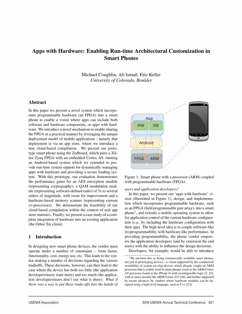
Figure 1: Smart phone with a processor (ARM) coupledwith programmable hardware (FPGA).
users and application developers?In this paper, we present our ‘apps with hardware’ vi-
sion (illustrated in Figure 1), design, and implementa-tion which incorporates programmable hardware, suchas an FPGA (field programmable gate array), into a smartphone1, and extends a mobile operating system to allowfor application control of the current hardware configura-tion (e.g., by including the hardware configuration withtheir app). The high-level idea is to couple software-like(re)programmability with hardware-like performance. Inproviding programmability, the phone vendor empow-ers the application developers (and by extension the endusers) with the ability to influence the design decisions.
Developers, for example, would be able to introduce
1We envision this as being commercially available smart phones,not just in prototyping devices – a vision supported by the commercialavailability of system-on-chip devices which already couple an ARMprocessor that is widely used in smart phones (such as the ARM CortexA9 processor found in the iPhone 4) with reconfigurable logic [5, 25],with or more recently the ARM Cortex A53 [26], and further supportedby recent advances by vendors where hardware modules can be de-signed using a high-level language, such as C++ [23].
1

622 2016 USENIX Annual Technical Conference USENIX Association
(and deploy) new communication technologies, such asthose that work on the emerging dynamic spectrum ac-cess paradigm [30], where they can perform ‘software’radio at the needed hardware performance levels andgain system wide benefits (e.g., from not needing phonesto include many dedicated radio interfaces). Devel-opers will also be able to introduce new accelerators,such as for cryptography or other parallel processingthat improve overall performance and efficiency. Fi-nally, developers will be able to introduce independentco-processors, which can, for example, provide addi-tional security [57] capabilities not possible in today’ssmart phones. In general, we introduce programmabil-ity of the smart phone hardware by creating an architec-ture centered on an FPGA with an embedded processor– with which, as we’ve seen with other programmabletechnology, such as graphical processor units (GPUs)and FPGAs in other contexts within the network systemscommunity, developers will find creative ways to use theavailable processing power [52, 59, 45, 41].
Previous research has proposed adding reconfigurabil-ity to mobile devices, such as [11] [61] [32], but theyhave limitations that prevent them from being used to-day, such as lacking a method to share FPGA hardware,a distribution system for applications, or integration intomodern operating systems or devices. Therefore, thereare a number of challenges that we need to address tomake our vision possible. First, we need to be able toshare an FPGA between different smart phone applica-tions – existing FPGA hardware and software are heav-ily centered on running a single application and not onidea of temporal or spacial sharing of resources. Second,we need a way to distribute apps with hardware to smartphones with compatible hardware – there is no binarycompatibility in FPGAs or operating system which ab-stracts resources. Finally, we need the ability to managethe FPGA so that applications only have access to au-thorized resources – while processors have been adaptedovertime to isolate running tasks, FPGAs have not.
In this paper we present our Cloud RTR system thataddresses these challenges. In doing so, we introduce asystem-level contribution that makes use of cloud tech-nologies and builds on existing FPGA technology thattogether solve a problem that has eluded researchers foryears. Specifically, we make the following contributions:A slot based solution that allows for practical FPGAsharing: A central need to be able to allow apps to spansoftware and the FPGA hardware is to enable the FPGAto be shared, as apps will be concurrently running. Ourapproach is based on Run-time reconfiguration (RTR),or the ability to change an FPGA’s configuration at run-time. Specifically, our Cloud RTR system builds on theidea of “slots” [38] [49] [42], or areas of the FPGA thatcan be reconfigured separately and shared between appli-
cations. To make this practical, where previous systemshave failed, we provide a new approach to slot-based re-configuration using a compilation system that abstractsaway the underlying FPGA requirements. The resultingplatform supports the use of slots at run-time, whereasprevious systems only support slots at design time, andcan share the FPGA between multiple parties, as we dis-cuss next. Further, we introduce operating system ser-vices to manage slots at run-time to allow for on demandaccess from apps.An app store based approach that allows for multipleparties to distribute apps: Without operating systemand binary compatibility, envisioning a system which al-lows for multiple parties to create apps and have them bedistributed to a wide variety of devices may seem diffi-cult. We introduce a new app-store system which extendsexisting app stores to to allow for both the compilationand the distribution of apps with hardware. Developerscan upload apps with hardware to an extended app store,which will interface with the compilation system in orderto generate the required slot configurations. We extendthe app store system further to ensure that these config-urations are distributed to the correct devices in pack-aged apps, and we provide corresponding operating sys-tem support in order to install them.A security manager that enforces access control tosensitive resources Our Cloud RTR architecture alsoprovides a secure loading subsystem that ensures thatonly trusted applications have access to sensitive re-sources. This subsystem interfaces with the slot run-timemanagement system to only allow for signed app hard-ware to access these resources. This system also usescommon hardware security technology to ensure that ap-plications cannot exploit the operating system to overridethese security restrictions.
In addition to the above system-level advances whichenable the apps with hardware vision, we make the fol-lowing contributions which evaluate and demonstratetheir use:Evaluation of the computational requirements ofCloud RTR: While our approach of performing somecompilation in the cloud is, to some degree, simplistic,the fact that it has not been done before does, we feel,point to its novelty. Importantly, we go beyond simplyproposing to compile in the cloud and extend our workto fully evaluate the computation requirements of suchan app store to support this using data about the currentapp market ecosystem. We show that for compilationthroughput per machine ranges from 51 to 121 apps perday, which translates to needing 1020 servers to supportan app ecosystem where 1 percent of all apps use the re-configurable logic for a case where there is 1000 phonevariants.Demonstration and evaluation of three applications:
2

USENIX Association 2016 USENIX Annual Technical Conference 623
In Section 2, we describe three example categories of ap-plications that will benefit from an apps with hardware.For each, we implemented and evaluated a representa-tive application (Section 6). Our evaluation of an appwhich offloads to a hardware based QAM module (a rep-resentative software-defined radio application) shows a40x speedup and a hardware based AES module (a repre-sentative cryptography application) shows a 3x speedup(including all of the interface between hardware and soft-ware). Additionally, our evaluation of a simple memorysecurity scanner (a representative architectural enhance-ment) that is capable of searching the entire system ad-dress space only results in 3% overhead for other soft-ware running. Finally, to understand the considerationswhen integrating into existing, complex, applications, wemodified the open source and widely used Orbot [17]Tor [37] client for Android to include and use a hardwarecryptography module (Section 7).
In the remainder of the paper we will further motivatethe proposal to incorporate an FPGA into a smart phone(Section 2), describe past FPGA sharing attempts (Sec-tion 3), and describe our system, including our CloudRTR architecture, which includes both the architecturefor our slot compilation and app store extensions (Sec-tion 4), our runtime management and secure loading ar-chitecture (Section 5. We then provide an evaluation(Section 6), describe our case study of the Orbot Torclient (Section 7), describe other related work (Section8), and then conclude (Section 9). We are also pro-viding the code for the entire implementation (compila-tion, applications, FPGA system, and Android enhance-ments) in a git repository: https://github.com/nsr-colorado/cloud-rtr.
2 Motivation (Why an FPGA)
The premise of incorporating an FPGA into a smartphone lies in the general benefits of an FPGA – that itprovides hardware-level programmability which will en-able phone manufacturers to defer some decisions abouttradeoffs to the end user and enable developers with theability to innovate in the hardware space.
Here we discuss a few examples that help motivate anFPGA within a smart phone, including a description of ademonstration application that we implemented for eachof these categories.
2.1 Architecture enhancementsFor our first set of motivating examples, we present sev-eral architectural enhancements that have been proposedin the research community that each required a hardwareplug-in and were targeted at a server. With our work,similar benefits could be brought to a smart phone. It is
important to note that FPGAs are not limited to stream-ing and highly parallel processing (though they do excelat that). These types of applications can implement secu-rity functions, which are supported by our secure loadingtechnology (discussed in Section 5).CoPilot: CoPilot [57] is a PCI card designed to de-tect rootkits. As rootkits execute at the highest privilege,detection mechanisms at the same (or lower) privilegeare presented with a significant challenge. The CoPilotPCI card is independent of the processor and operatingsystem and has access to all memory via the PCI bus.Rootkit detection (or more generally, security applica-tions) have tremendous potential with the introduction ofan FPGA within a smart phone.Somniloquy: The Somniloquy [27] work observedthat the energy consumption on servers was impactedby a number of low-rate type of tasks that prevented theservers from entering the power saving states. As such,they proposed a small, low-power processor that couldperform these tasks, and if needed, trigger the main pro-cessor to exit a low-power state. In the case of a smartphone with an FPGA, similar types of activity has beenobserved in smart phones [31], so a small co-processorin the FPGA fabric could provide a solution (while alsoenabling the main processor to shut off completely). Weleave full exploration of power as future work.
As a demonstration of architectural enhancements, wehave implemented a memory scanner module, as a sim-plified proxy for a CoPilot-like function, that scans ourdevice’s system address space.
2.2 Software-defined RadioA great deal of research has resulted in many innovationsin wireless communications which allow wireless inter-faces to have better performance or more functionality.Research papers in this space commonly use FPGA plat-forms (such as the WARP Board [28, 53]), or devices tointerface to high performance desktop machines (such asthe USRP [22]) in order to meet the needs of the newinnovation. While these papers provided promising re-search results, there is little opportunity for deployment– requiring the researchers to commercialize the technol-ogy, or get adoption from a major chip vendor.
With a smart phone that has an FPGA along with amore flexible radio front end (e.g., a tunable antenna), de-velopers of a new communication protocol could simplycreate an app, enhancing the impact of the research. Thisarchitecture also has benefits for production systems, asexisting devices could be upgraded to new wireless sys-tems without requiring replacement, such as upgradingsuch a system from 3G to 4G wireless technology.
As a demonstration of an SDR application, we haveincluded an example implementation of a Carrier Phase
3

624 2016 USENIX Annual Technical Conference USENIX Association
Recovery Loop for a single carrier Quadrature Ampli-tude Modulation (QAM) demodulator. QAM is a repre-sentative building block in signal processing applicationsincluding many real-world modulation systems.
2.3 Cryptographic and Parallel Processing
FPGAs have the ability to perform large amounts of pro-cessing in parallel. This allows them to achieve higherthroughputs and lower latencies.
An exemplary application for FPGA acceleration on asmart phone is cryptographic processing, as it both fasterin an FPGA and widely used – including the encryptionof internet communication using SSL and communica-tion protocols such as Tor [37], the accountable inter-net protocols [29], and Named-data Networking [44] Forexample, an FPGA (Altera Stratix V) was shown to be520 times faster than a general purpose processor (IntelXeon E5503) for AES encryption (and 15x speedup overan AMD Ratheon HD 7970 GPU) [4]. While the exactnumbers will depend on a number of factors, this is illus-trative of the potential.
Parallel processing goes beyond cryptography. Onerecent example used an FPGA based server [10] to im-plement common functions used in analytics (search,fuzzy search, and term frequency), and in each casedemonstrated that it would require 100-200 servers run-ning Spark [65] to match the performance. This exampleis really geared towards cloud scale applications, but webelieve this would allow us to perform some analytic pro-cessing locally (on the phone) without needing to sendprivate data to some cloud based backend.
As an example of this type of application, we have im-plemented a 128-bit AES encryption module that can en-crypt an arbitrary number of 128-bit contiguous regionsof memory. We also incorporated this AES module intothe Orbot Tor client (Section 7).
3 Past Attempts
A central challenge in reaching our vision relates to howto share the FPGA between applications and the system.That is, we wish for multiple apps to be able to simul-taneously use some of the FPGA’s programmable fabric,while at the same time allowing the operating system touse some of the programmable fabric as well (e.g., toconnect to some I/O devices).
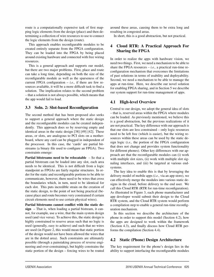
The core concept required is run-time reconfiguration,or the ability to dynamically change the FPGA’s configu-ration (completely or partially) at run-time while it is stilloperating. Despite over a decade of research in run-timereconfiguration [33, 39, 48, 34, 36, 51, 62, 43] there hasyet to be a practical solution which would enable hard-
CPU
Possible location to put module
Hardware module
FPGA
Wire resourcecontention (red)
Figure 2: Example of partial reconfiguration in a runningFPGA configuration.
ware modules from various sources to be loaded onto avariety of platforms.
3.1 Why is sharing an FPGA difficult?The main challenge in achieving FPGA sharing is ensur-ing that the apps’ modules in the FPGA do not conflictwith each other, or with other logic that is present in theFPGA. FPGAs are difficult to share because a complexmapping of resources must occur in order to generate aconfiguration for an FPGA. This is because application’slogic must be mapped to physical resources in the FPGA,and connections must be made between these locations,just as in any physical circuit.
As an example, consider Figure 2, which illustratesa single module to be loaded into an FPGA at run-time.The dotted area indicates one possible location to put thatmodule. As indicated, however, there will be contentionfor resources – i.e., this module cannot co-exist with thecurrent FPGA configuration. Because of this, the par-tial reconfiguration mechanism supported by the vendors(Altera and Xilinx) comes with great restrictions – themodules can only work with a single design (in our case,they wouldn’t work across phone architectures), and theycan only be loaded into a single location. These restric-tions make partial reconfiguration unusable in its currentform to enable apps with hardware.
More general run-time reconfiguration approacheshave been proposed in the research community that fallinto one of two categories, which we describe next. Ingeneral neither of these approaches are practical.
3.2 Soln. 1: Run-time Place and RouteThe first approach is to perform place and route at runtime [60] [46] [56] (rather than when it is normally per-formed – at design time). As background, place and
4
USENIX Association 2016 USENIX Annual Technical Conference 625
route is a computationally expensive task of first map-ping logic elements from the design (place) and then de-termining a collection of wire resources to use to connectthe logic elements from the design (route).
This approach enables reconfigurable modules to becreated entirely separate from the FPGA configuration.They can be loaded into the FPGA by being placedaround existing hardware and connected with free wiringresources.
This is a general approach and supports our model,but there are two major problems. First, place and routecan take a long time, depending on both the size of thereconfigurable module as well as the sparseness of thecurrent FPGA configuration – i.e., if there are few re-sources available, it will be a more difficult task to find asolution. The implication relates to the second problem– that a solution is not always possible, which means thatthe app would fail to load.
3.3 Soln. 2: Slot-based Reconfiguration
The second method that has been proposed also seeksto support a general approach where the static designand the reconfigurable modules can be created indepen-dently. This approach does so by reserving empty andidentical areas in the static design [38] [49] [42]. Theseareas, or slots, are analogous to PCI slots on a mother-board, where any card can be plugged in independent ofthe processor. In this case, the ‘cards’ are partial bit-streams (a binary file used to configure an FPGA). Twoconstraints emerge:Partial bitstreams need to be relocatable – So that apartial bitstream can be loaded into any slot, each areaneeds to be identical. This is not difficult from a logicstandpoint as FPGAs are fairly regular structures. In or-der for the static and reconfigurable portions to be able tocommunicate, however, there need to be wires that crossthe boundaries which, in turn, need to be identical foreach slot. This puts incredible strain on the creation ofthe static design, to the point of not being practical (be-cause place and route becomes very constrained if certaincircuit elements need to use certain physical wires).Partial bitstreams cannot conflict with the static de-sign – That is, when loading a partial bistream, it can-not, for example, use a wire, that the main system designused (and vice versa). To achieve this, the static design ishighly constrained to reserve areas such that no logic isused (generally, easy to achieve) and such that no wiresare used (in Figure 2, this would mean that static portionof the design would not have been allowed the wires thatare in the dotted area). Such constraints are ultimatelypossible (through a painstaking process of reverse engi-neering and over-constraining), but highly constrains thestatic portion of the design – forcing wires to be routed
around these areas, causing them to be extra long andresulting in congested areas.
In short, this is a good abstraction, but not practical.
4 Cloud RTR: A Practical Approach ForSharing the FPGA
In order to realize the apps with hardware vision, weneed two things. First, we need a mechanism to be able toshare the FPGA resources – i.e., a practical run-time re-configuration mechanism that overcomes the limitationsof past solutions in terms of usability and deployability.Second, we need a mechanism to be able to manage theapps at run-time. Here, we describe our novel solutionfor enabling FPGA sharing, and in Section 5 we describeour system support for run-time management of apps.
4.1 High-level OverviewCentral to our design, we adopt the general idea of slots– that is, reserved areas within the FPGA where modulescan be loaded. As previously mentioned, we believe thisis a good abstraction, but the previous realizations of itare not practical. The key difference with our approach isthat our slots are less constrained – only logic resourcesneed to be left free (which is easier), but the wiring re-sources within these areas can be used by the static de-sign logic (i.e., the portion of the FPGA configurationthat does not change and provides system functionalityfor different phones). Other key differences with our ap-proach are that the reconfigurable modules can (i) workwith multiple slot sizes, (ii) work with multiple slot sig-naling interfaces, and (iii) be targeted at various end-systems.
The key idea to enable this is that by leveraging thedelivery model of mobile apps (i.e., via an app store), wecan effectively merge the modules into various static de-signs in the cloud, before delivery to the end user. Wecall this Cloud RTR (RTR for run-time reconfiguration).As illustrated in Figure 3, each phone manufacturer andapp developer would submit their design to the CloudRTR system, and the Cloud RTR system would performa compilation step to enable a general run-time reconfig-uration mechanism.
In this section we describe the architecture of thephone in order to support this model (Section 4.2), howthe apps are designed to work within the framework(Section 4.3), and finally discuss how Cloud RTR per-forms the compilation (Section 4.4).
4.2 Static (Phone) Design ArchitectureThe key requirement for the phone’s design lies in theability to support interfacing the reconfigurable modules
5

626 2016 USENIX Annual Technical Conference USENIX Association
storedapps
DeveloperUser device
PhoneManufacturer
Front End(app store)
CloudCompiler
storedvariantsapp
sw.bit.bit
.bit.bit
phone2
phone1
Netlist, app software
app package(with hw)
Cloud RTR
phonehw design
Figure 3: Cloud RTR approach to the generation and deployment of apps with hardware
Memory
CPU
Slot
Mem Controller
access control
DMA
System Bus
Slot
CLB,DSP,BRAM
processor subsystem
programmable fabric
Device interfaces
(e.g., HDMI, RF)
embeddeddevices
(e.g., UART)
Figure 4: Example static FPGA design.
with the rest of the system resources. Illustrated in Fig-ure 4, and described below, are the main components.Slots
Slots should have enough of all types of resources tobe useful. Today’s FPGAs can contain (i) configurablelogic blocks (CLBs), which can implement any logicfunction of N inputs, (ii) block random access memory(BRAM), which are small memory elements (e.g., 36 Kbin the FPGA we use for implementation), and (iii) digitalsignal processing (DSP) blocks, which are custom build-ing blocks geared toward signal processing applications.
Slots will also need to be able to access various sys-tem resources and expose an interface for communica-tion with the processor. For this, we expect that all slotswill allow access to (i) a system bus for communica-tion with the processor, and (ii) a direct memory access(DMA) controller for access to system memory.Module-to-Memory Interface
In order to provide performance benefits, the modulesneed to be able to directly access CPU-accessible sys-tem memory. A DMA controller that is accessible bythe hardware modules would allow for modules to access
system memory without involving the processor (provid-ing the greatest performance and flexibility). To achievethis, we also need a security module which performs ac-cess control – that is, one which limits what memoryeach hardware module can access and is configured bythe operating system.Processor-to-Module Interface
The ability to stream from memory will be important,but the processor also needs to be able to directly inter-face to each module. This interfacing is achieved throughthe use of, for example, a system bus (such as the ARM-based Advanced eXtensible Interface, or AXI).Device interfacing and other misc. logic
The rest of the static design will include interfacing tothe various devices that will connect to the FPGA. Somedevices, such as a UART, may have interface logic in-cluded in the processor sub-system, but the rest, such asinterfacing to a tunable antenna, may go through the pro-grammable fabric with custom logic to interface with it.These devices will be connected to the general interfaceof the slots, allowing for manufacturers to include cus-tom peripherals without requiring new slot definitions.
4.3 Reconfigurable (App) Module Archi-tecture
In the previous slot-based approaches, the reconfigurablemodules are designed for a specific slot design (device,interface, etc.). In our approach, we abstract away theultimate target such that app developers can develop re-configurable modules that can be loaded onto a varietyof platforms. Of note, the reconfigurable modules in ourapproach can (i) work with multiple slot sizes, (ii) workwith multiple slot signaling interfaces, and (iii) be tar-geted at various end-systems.
Here we describe the design of an app, with the variouscomponents illustrated in Figure 5.
6

USENIX Association 2016 USENIX Annual Technical Conference 627
App HardwareThe first major component is the app hardware. In
order to match the skills of app developers, we focus onthe high-level synthesis (HLS) design flow [23] that hasemerged in recent years which allows developers to use ahigh-level language (e.g., C) to describe hardware mod-ules2. What this means is that the argument that FPGAsare hard to design for, and therefore not accessible to thesoftware app developers, is quickly becoming invalid.
The app hardware (in this example) is written as a C++function, example(). The parameters to the function de-scribe the interfaces to the rest of the system, such aschar arrays (e.g., var1), which describe memory mappedregisters accessible to the processor or streaming mem-ory interfaces (e.g., var2, which has the type hls::stream),that allow for streaming data from memory (when con-nected to DMA hardware in the static design). This de-scription is valid C++ code that can be compiled andtested as software which can simplify hardware testing.
While there will need to be some consideration by de-velopers, in general developers will not need to be fullyaware of the hardware architecture. For example, theexact bus signals for communicating with the moduleare not directly used, but are instead inferred based onthe types on the function parameters (such as how toperform data transmission handshakes or send valid sig-nals). With this, the same module could actually targetvarious hardware interfaces (e.g., if different handshakeprotocols or signals are used, or if different bus widthsare available). Developers do need to consider the size(resource utilization) of their hardware modules to en-sure they will fit in a particular slot size. We envisionstandard slot sizes will emerge (much like screen sizes),and in our design flow we allow for modules designed forone slot size to always be instantiated in a bigger slot.App Software
The app software that the developer writes will bemostly the same as current apps (e.g., written in Java forAndroid apps). The only difference is the loading of andinterfacing with the hardware module. To load, the appwill submit a request to a system service to load the bit-stream (e.g., via an intent in Android).
To interface with the module, the app will use the func-tions in the user-level driver generated by the FPGA ven-dor’s high-level synthesis tool when synthesizing the de-sign (the process which generates the FPGA hardwarefrom the C++ code). This driver is low-level code thatruns within the same process as the application and pro-vides functions that can be used to interface with thereconfigurable module. Functionality includes mappingmemory regions (e.g., via mmap()) that both the recon-
2The developer can use a hardware description language, but willthen need to manually provide the interfacing hardware and software,which are automatically created with high-level synthesis.
Tools
RegisterDMA
Circuit
to mem
JNI
Java// app codeload modulealloc shared memcall set/get_var1poll/interrupt…
// user level driverset_var1(val)…
Software code
int example(char[] var1, hls::stream var2) {
…}
Hardware code
generated netlist
Figure 5: Example app design.
figurable module and the app will access. It also providesfunctions to access the various registers (the char[] vari-able) through functions like set var1().
4.4 Cloud Compiler (in the App Store)The Cloud RTR compiler is responsible for ensuring thatan app’s hardware module(s) can be loaded into a vari-ety of target devices (smart phones). Rather than work-ing around the limitations of the vendor tools, we workwithin their constraints, resulting in a practical solution.Recall that the vendor tools have a partial reconfigura-tion design flow which has the constraints that a modulecan only be used for a specific static design and targetFPGA and for a specific location within that static de-sign. Working within that, the Cloud RTR compiler willsimply use the vendor tools to compile the module for ev-ery static design variant and for every possible slot withineach variant.
The end result is a data structure stored within the appstore that looks like the following (where a.bit...e.bit areindividual partial bitstreams):
[phone 1:
[slot1:a.bit, slot2:b.bit, slot3:c.bit]]
[phone 2:
[slot1:d.bit, slot2:e.bit]]
When an app is downloaded to a given device, theCloud RTR system will repackage the application withthe set of device-specific bitstreams (possible since theapp store has knowledge of a user’s device). In Android,for example, apps are packaged in an Android Applica-tion Package (APK), which will now include module bit-streams as extra resources for apps that use hardware. Toget a rough idea of how this impacts the size of an APK,for the case study we describe in Section 7, the hardware
7
628 2016 USENIX Annual Technical Conference USENIX Association
module bitstream is 904KB, the Orbot APK of the ver-sion we modified is 5.5MB (before any added hardware),and the latest Orbot release is 11MB.
We show that this brute-force approach is quite practi-cal in Section 6. As such, it provides a general approachthat is deployable and usable today. In addition, we alsoenvision a large amount of reuse of both static designsand hardware modules (e.g., by using precompiled li-braries). Just as SoCs are oftentimes reused between dif-ferent mobile devices, there is no need to have a distinctstatic design for different devices unless a particular de-vice requires some custom technology.
5 Run-time Management of Apps
With the ability to share the FPGA, as provided by CloudRTR, we now discuss how our system manages the apps’hardware within the Android operating system. This hastwo aspects – (i) how to dynamically manage the load-ing and unloading of hardware modules for various apps,and (ii) how to ensure the modules cannot compromisethe running operating system and vice versa. We achievethe dynamic management by modifying the Android op-erating system to include a system service that managesthe loading and unloading of modules and enables ap-plication software to access these modules. Our secureloading system takes advantage of some hardware secu-rity features of modern FPGAs and some hardware in thestatic design in order to provide the needed security.
5.1 Dynamic Module Loading ServiceTo support apps with hardware, there needs to be systemsupport for loading hardware modules into the FPGA.The operating system will have access to our secure load-ing system (described in the next section) that can take ahardware module compiled using the Cloud RTR systemand load it into the FPGA. However, user applicationswill not have direct access to this system.
User applications will instead submit requests througha privileged hardware loader system service. Upon load-ing and initialization of the app, the service will be pro-vided with the location of the app’s hardware modulefiles. The service will then choose an empty slot, se-lect the module compiled for this slot, and use the secureloading module to load the module into the FPGA. In thecase where no slots are available, the operating systemcan create ‘virtual’ slots by time-slicing existing slots.Given the slot reconfiguration time, we do not expect toswap app hardware as frequently as app software, but wesee this is an area for future consideration.
We can implement virtual slots by using the readbackcapability of FPGAs to store the running configurationof modules, and developers can provide custom unload
functionality to aid the readback system in storing diffi-cult to access state (specifically, certain FPGA memoryis more difficult to access). Applications that would bedisrupted by time slicing can be specifically flagged asunsafe to swap, but the number of these applications run-ning simultaneously should be restricted.
The time to load a hardware module provides an es-timate of the time needed to context switch a hardwaremodule. This time is a function of the size of the hard-ware being written to the FPGA, which we measured tohave an average throughput of 37 MiB/s. This leads toa latency of approximately 100 ms for a 4 MB static bit-stream, or 27 ms for 1 MB hardware module.
The hardware module is presented as a devfs characterdevice in the Linux /dev directory (when using Android).The hardware loading service will set file permissions toensure that only the application that requested the load-ing of the hardware module can access it.
5.2 Secure Loading
We introduce a secure loading mechanism to providesupport for protecting both the operating system fromapp hardware and the FPGA configuration from the oper-ating system (e.g., a rootkit). Our secure loading mech-anism is an extension of secure boot technology where(i) we disable the processor’s connection to the config-uration ports of the FPGA, and (ii) we add a modulewithin the static design to support loading of app hard-ware. For space purposes we can only sketch the high-level overview of the secure loading.Threat model and assumptions: We assume that anycode running on the CPU, including the operating sys-tem, can be malicious. We also assume that even withthe support of modules such as the trusted platform mod-ule (TPM) to protect the booting of the operating system,malicious code can be executed at run-time that can com-promise the operating system. We assume that some re-configurable modules will be untrusted and potentiallymalicious. We assume that some reconfigurable moduleswill be trusted (from trusted sources, such as the phonemanufacturer) and will not be malicious. Finally, we as-sume that the static FPGA configuration is trusted andcorrect at boot time (through secure boot mechanismssupported by modern FPGAs [64]). With this, we as-sume the keys of the app store and an additional trustedparty are present at boot and cannot be modified.
The secure loading can be summarized as follows:
• Secure boot technology of the FPGA will load atrusted FPGA configuration as well as ensure theoperating system is known to be good at boot.
• As part of the secure boot, the processor will haveits access to the configuration ports disabled (e.g.,
8

USENIX Association 2016 USENIX Annual Technical Conference 629
the processor configuration access port, PCAP, andthe internal configuration access port, ICAP).
• A hardware secure loading module, part of the staticconfiguration, will accept requests to load a recon-figurable module from the operating system .
• Every module will be signed by the app store. Fromthis the hardware secure loading module will verifythe signature in order to ensure that the configura-tion refers to is the slot to be loaded (preventing thecase where an app was modified to include a con-figuration which overwrites parts of the FPGA otherthan the allocated area).
• For trusted modules (which will signed by the appstore and by an additional trusted party), the hard-ware secure loading module will verify the signa-ture and if it succeeds, configure the memory ac-cess control to allow the module to have access tosystem memory. Trusted modules will not be ableto be unloaded or overwritten without a reboot.
• For untrusted modules (which will be signed by theapp store, but not by an additional trusted party), thehardware secure loading module will configure thememory access control to restrict access to memory.
With this process, we get the following properties:
• Modules will be correctly loaded only into the slotsfor which they are supposed to be loaded and notoverwrite any static configuration.
• Code in the operating system cannot load a mod-ule in a slot which gets access to system memory(preventing app hardware from helping apps bypasssystem protections, or otherwise harm the system).
• Code in the operating system cannot overwrite orunload a trusted module (preventing rootkits, for ex-ample, from unloading security modules meant todetect the presence of rootkits).
6 Evaluation
There are two main questions to answer, which we dis-cuss in this section:Is there value in apps with hardware?
There’s general acceptance that hardware will be fasterthan software3. The question we seek to answer hereis whether the same performance benefits are retainedwhen we consider it within a system (e.g., does crossingthe hw-sw boundary make things worse).
3That’s not really the focus of our paper – we take the stance thatthere are places where each wins (FPGA, CPU, GPU) and that het-erogeneous architectures are good, and more importantly open pro-grammability is what drives innovation.
Figure 6: The execution time to perform an AES encryp-tion for a range of data sizes – from 10 to 13000 contigu-ous 128-bit (16-byte) segments of memory.
Is the cloud compilation of Cloud RTR practical?As mentioned, rather than continuing the path of run-
time reconfiguration research, which leads to creative,but impractical solutions, we aimed for a solution whichwas highly practical and deployable today. This resultedin a brute force approach. Here, we ask whether this isitself practical by examining the processing required tosupport the app market ecosystem.
6.1 Application Performance AccelerationPerformance acceleration is one of the benefits of usingan FPGA. Of course, we also believe that new applica-tions are now enabled, such as our hardware-based mem-ory scanner. We focus on performance here as a concretedemonstration with a quantitative evaluation.
We focus on three key application domains that are en-abled. Each of these applications consists of a hardwaremodule written in C++ using high-level synthesis and anAndroid application that interfaces with the module. Werun the hardware module through the Cloud RTR com-pilation platform targeting the static design for our de-velopment board. The end result is an APK that can beloaded into our demonstration board. Each applicationfit within our slots, which we defined at 12% of the over-all FPGA area – a number resulting from dividing theremaining area after what is needed for the static designby six available slots.
For our experiments, we protoyped a mobile deviceusing the Zedboard development board, which integratesa Xilinx Zynq 7020 FPGA [25] that has an embeddeddual-core ARM Cortex-A9 CPU. We based our Androidservices on the Android 2.3 and 5.0.2 operating systemsthat were already ported to our device.
6.1.1 Cryptography: AES
In Figure 6, we compare three different AES implemen-tations using our development board, and running An-
9

630 2016 USENIX Annual Technical Conference USENIX Association
droid as the operating system on the CPU4:
• FPGA (ours) – an AES FPGA reconfigurable mod-ule accessed by an Android application in nativecode using the the Java native interface (JNI).
• OpenSSL – the OpenSSL AES implementationwhich we interfaced directly from a C application.
• Android AES – the AES implementation providedto Android applications by the AOSP.
This figure shows the execution times of the AES im-plementation (which we derived from [1], though wealso experimented with versions from Apple [2] andNIST [3], which had identical performance) for a rangeof data sizes to be encrypted, varying in size from 10 to13000 contiguous 128-bit segments of memory. It can beseen that the FPGA implementation is on average threetimes faster than the OpenSSL implementation, and isapproximately 12 times faster than the AOSP. However,the execution time of the FPGA module as measured byJava (marked in red circles) and executed using the JNI islonger than the execution time of the same module whenexecuted directly by a C program (marked in blue dia-monds). This is likely due to overhead entailed in copy-ing memory to the JNI function call and transferring con-trol to the JNI. This can potentially be alleviated usingJava direct byte buffers passed directly to the JNI func-tion, but is deferred to future work.
6.1.2 Software-defined Radio: QAM
This application can process a signal stored in a contigu-ous memory region and produce an output signal that isstored into another contiguous region. In a live smartphone, the static design would place the signal off of theantenna into buffers in memory, notify the Android ap-plication of a buffer being full, and the application wouldpass this data to the QAM module. The number of sam-ples the QAM block can process determines the samplerate of the radio application. We implemented this mod-ule by modifying (to be compatible with our Cloud RTRsystem) a reference Xilinx project [55], which comeswith C++ code that can be executed in software or runthrough high-level synthesis to produce hardware.
As shown by Figure 7, the hardware implementationis several orders of magnitude faster than the softwareimplementation. The hardware implementation achievesan average throughput of approximately 5 Msps (mega-samples per second), while the software implementationonly achieves and average of approximately 500 sam-ples/s. The Xilinx application notes claim a throughputvalue of 50 Msps [55], which is likely achievable due tothe fact that the hardware device is intended to process
4 We also performed the OpenSSL benchmark in Ubuntu Linux toconfirm that the Android OS does not institute a performance penalty.
Figure 7: The execution time to process a different num-ber of samples with our QAM application.
data received directly from an analog-to-digital converter(ADC), whereas our implementation has been retrofittedto stream data from system memory.
6.1.3 Memory Scanner
Our final application is a simple implementation of ahardware memory scanner that searches our device’s ad-dress space for occurrences of a 16 byte string. We wrotecustom C++ code that we ran through high-level synthe-sis for this implementation.
Using the LMbench testbench [50], we instituted amemory benchmark that measured the throughput ofour device’s memory while under normal operationand while the hardware memory scanner was executing(which is constantly reading from memory). Using thisbenchmark, we measured a 2.7% reduction in perfor-mance for read operations and a 5.5% reduction in per-formance for write operations.
6.2 Cloud Compilation Resources NeededWe propose performing compilation of the reconfig-urable module in the cloud as part of the process to up-load to the app store. To understand the feasibility ofthis, here we evaluate the amount of computing resourcesneeded to sustain an ‘apps with hardware’ ecosystem.
The metric of interest is how long it takes to compilea single reconfigurable module for a given static design.Recall that a static design is the base design that roughlycorresponds to a system on chip used for a given smartphone. These static designs have open areas (slots) forplacing reconfigurable modules.
For all experiments, we used a server with an IntelXenon CPU (2.1 GHz, 6 cores, 48 GB RAM).
6.2.1 Single App for a Single Static Design
An app with hardware uploaded to the app store musthave its hardware modules compiled for each slot that it
10

USENIX Association 2016 USENIX Annual Technical Conference 631
# of slots Compilation Time (min) Throughput (apps/day)2 11.92 1213 14.93 964 19.02 765 24.21 596 28.23 51
Table 1: Compilation time and number of apps a singleserver could service per day.
6 Slots Requirement % of Jan 2016 Apps that Use Hardware0.1 1 10
# of Apps Uploaded per Day5 52 520
# of Static Designs # of Machines Required to Compile RMs1 1 1 1010 1 10 102
100 10 102 10201000 102 1020 10200
Table 2: Number of servers required to support the com-pilation requirements of Cloud RTR, assuming designswith six slots.
can be placed into. However, certain steps in the processdo not need to be performed for each slot – e.g., syn-thesis needs to be performed once for each module, thenfor each slot, the synthesized module needs to be placedand routed. For this evaluation we used an FFT module,which is a highly regular structure and enabled us to ad-just its parameters to effectively alter its size to fill upany slot size we experimented with.
Table 1 shows the total time to compile a single ap-plication’s reconfigurable module for static designs withtwo to six slots (each slot is defined as 12% of the over-all area of our FPGA, as previously mentioned), as wellas the extrapolated throughput (the number of apps thatcould be compiled per day on one server given this com-pilation time). We chose up to six slots (in contrast to the60-100 slots in [38]) as we believe each to be big enoughto implement a reasonable module within a single slot.
6.2.2 Compiling All Apps
Using the calculated throughput, we can now estimatethe amount of computing resources needed to service theentire app ecosystem.
First, we need to know how many apps are uploadedeach month. The company AppFigures provided us withthe Google Play Store application upload figures for theentire year of 2014, with a total of 1.43 million appsat the end of 2014, and an average monthly growth of6.10%. While we are unsure if this growth rate persistedover the past year, we use it to estimate the current needs.Using this average monthly app growth, for the month ofJanuary 2016, 177,521 applications are predicted to beuploaded into the Google Play Store.
Table 2 shows the number of machines required to
service monthly demands for compiling apps with hard-ware, for six slots as an example (2-5 slots would be pro-portionally less). Each table varies the number of appswith hardware uploaded each day based on the percent-age of applications that require hardware (0.1%, 1%, and10%), as well as the number of static hardware variants –for the sake of illustration, we assume from one to 1000variants, with each interval increased by a factor of ten(we expect the number of variants to be on the low end,as static bitstreams can be reused between devices, justas phones today use a small set of SoCs, and not everydevice will require a new static bitstream).
The cloud provider will easily be able to support thelower end of the spectrum internally. On the upper end,the cloud provider might look to relieve the computationburden by offloading to the phone manufacturers to com-pile for their own variants.
7 Case Study: Orbot Tor Client
Developing our demonstration applications from scratchallows us with to design it to use an FPGA natively. Herewe explore modifying an existing, complex applicationto make use of a hardware module to understand the in-efficiencies that may result.
We chose to modify the Orbot [17] Tor [37] client forAndroid. Tor is an anonymization network that allowsfor a user to access the internet without disclosing theirsource IP address, making identifying and tracking theirinternet traffic very difficult for third parties. A Tor clientcreates a circuit through this network and encrypts theirtraffic separately for each node along the path to preventeavesdropping during transmission. Because of this ex-tensive use of encryption and based on notes by the Or-bot developers mentioning that AES is one of the areasto optimize Orbot [21], we see this as an ideal case study.
Our AES module implements the CTR (counter) modeof operation on top of a standard AES block cipher that isan equivalent to the OpenSSL CTR implementation usedby Tor. In order to integrate our AES accelerator withTor, we replaced all calls to OpenSSL AES encryptionwith calls to the FPGA accelerator, which proved to be afairly minor modification. We also needed to ensure thatall data that was to be encrypted was located in a con-tiguous memory region with a known physical address,which required us to replace all malloc() calls with callsto a custom memory allocator, and leverage a memoryregion that we reserved from the kernel.
With this, the application is able to make use of theFPGA resources and operate correctly. However, thereare inefficiencies remaining due to (i) the overhead re-quired to allocate memory in the reserved region, (ii) theoverhead in accessing this memory, as it is implementedusing memory-mapped I/O, and (iii) the fact that certain
11

632 2016 USENIX Annual Technical Conference USENIX Association
memory system calls (e.g., malloc(), memcpy() and mem-set()) are incompatible with the current memory mappedimplementation – which would require more extensivemodifications to the code to resolve. Even so, this pro-vides us with great insight into how apps should be de-signed to capitalize on the FPGA resources and is an areafor future improvements.
8 Related Work
Although there are no existing systems that implementall of the functionality of our Cloud RTR system in mo-bile devices, there has been much work done in recon-figurable computing in other contexts, including severaldifferent attempts with Android.
Of note from previous reconfigurable computing re-search is the BORPH system [62], which attempts to cre-ate operating system extensions in Linux for FPGA op-erations, and uses Berkeley’s BEE2 system [35], and themore recent Connectal framework [47], which can auto-matically generate HW/SW interfaces during hardwaredevelopment. These systems, however, do not addressapplication distribution or FPGA resource sharing.
In terms of mobile systems research, some proposalshave been made, such as the rSmart system [63] and thework from Smit et. al. [61]. Smit et. al. proposes a simi-lar hardware architecture to the Zynq-7000 architecture,but does not present an operating system integration or adeployment system. The rSmart system only presents ahigh-level sketch of a system similar to ours, but no de-tails on implementation or integration are provided. Oursystem builds upon this research to create a general sys-tem that is deployable using existing technology.
There has also been recent advantage in reconfigurablecloud platforms. For example, Microsoft’s Project Cat-apult makes use of of FPGA peripherals in data cen-ters to accelerate web searches [58] and neural networks[54], and Intel’s acquisition of Altera [13] is leading tox86 CPU architectures coupled with FPGAs [40]. Mi-crosoft’s solutions, however, are only single-applicationhardware accelerators, whereas our system allows for us-age in general applications. Intel’s system is more gen-eral, but has not been released publicly, but does claim touse OpenCL [16] as the software interface.
Our work is complimentary. For example, OpenCLcan be used on mobile devices with support from majorhardware manufacturers, such as ARM, Intel and Qual-comm, [14] [20] [8] [12] [18], and can even be usedwith our system by using a compatible hardware module.OpenCL’s main limitation is its focus on parallel acceler-ation, which does not enable new architectural enhance-ments, such as our SDR or security applications.
Reconfigurable Android devices and systems havealso been proposed, such as Google’s Project Ara [11],
among others, including various other modular phones[19] [9] [15]. These modular phone systems allow forreconfiguration and upgrading of smart phone physicalcomponents, similar to how personal computer compo-nents can be upgraded. However, these modular architec-tures can only be reconfigured manually by the user re-placing the physical modules, whereas our system allowsfor dynamic and custom reconfiguration by software.
Finally, the Android OS has been ported to the Zynq-7000 in several projects, such as the work of Barbareschi,et. al., among others [32] [7] [6] [24]. However, withthe exception of the work of Barbareschi, et. al., theseprojects only port the OS to a new device. The work ofBarbareschi, et. al. only extends this work to create anAndroid-compatible custom accelerator to address a sin-gle problem, whereas our system allows for any generalsoftware to create their own custom hardware modules.
9 Conclusions and Future Work
In this paper we presented the concept of ‘apps withhardware’ where, with the introduction of an FPGA intoa smart phone we can enable app developers to innovatein the architectural (hardware) space, as they can todayin the software space. Our Cloud RTR cloud based com-pilation mechanism overcomes past limitations of usingthe FPGA in a general way and does so without requiringany modifications from the vendors (making it deploy-able today). Our Android-based run-time applicationmanagement system enables the dynamic managementof the execution of apps (and their use of the availablehardware), and provides a secure loading mechanism.
There is a great deal of possible future work. First,performing a thorough power analysis in a fair man-ner will provide great insight into both the benefits andneeded system support, and building more apps to cap-italize on the new capabilities would likewise providegreat insight. Second, we wish to work with additionaltools from other vendors (e.g., Altera) and operating sys-tem platforms to explore implementation differences andwith a partner to develop an actual prototype smart phonesystem (rather than the Zedboard) to further understandits viability. Finally, we wish to further investigate mem-ory management techniques for better optimization.
10 Acknowledgments
This research was supported in part by NSF SaTC grantnumber 1406192. We would also like to thank PhilJames-Roxby and Derek Woods for their guidance, andXilinx for their hardware and software donations.
12
USENIX Association 2016 USENIX Annual Technical Conference 633
References[1] http://programmablelogicinpractice.com/?p=87.
[2] http://www.opensource.apple.com/source/CommonCrypto/CommonCrypto-55010/Source/
libtomcrypt/src/ciphers/ltc aes/aes.c.
[3] http://csrc.nist.gov/archive/aes/rijndael/Rijndael-ammended.pdf.
[4] 40Gbit AES Encryption Using OpenCL and FPGAs.http://www.nallatech.com/40gbit-aes-encryption-using-opencl-and-fpgas.
[5] Altera socs. https://www.altera.com/products/soc/overview.html.
[6] Android 4.2.2 on zynq getting started guide. http:
//www.wiki.xilinx.com/Android+4.2.2+On+Zynq+Getting+Started+Guide.
[7] Android on zynq getting started guide. http:
//www.wiki.xilinx.com/Android+On+Zynq+Getting+Started+Guide.
[8] ARM Mali OpenCL SDK. http://malideveloper.arm.com/resources/sdks/mali-opencl-sdk/.
[9] Fairphone. https://www.fairphone.com/.
[10] FPGA System Smokes Spark on Streaming Analytics.www.datanami.com/2015/03/10/fpga-system-smokes-spark-on-streaming-analytics/.
[11] Google Project Ara. http://www.projectara.com/.
[12] GPGPU OpenCL API. http://www.vivantecorp.com/index.php/en/technology/gpgpu.html.
[13] Intel Altera Acquisition. https://newsroom.intel.com/news-releases/intel-completes-acquisition-of-
altera/.
[14] Intel OpenCL SDK. https://software.intel.com/en-us/intel-opencl.
[15] LG G5. http://www.lg.com/us/mobile-phones/g5.
[16] OpenCL. https://www.khronos.org/opencl/.
[17] Orbot. https://guardianproject.info/apps/orbot.
[18] PowerVR SDK. https://community.imgtec.com/developers/powervr/.
[19] Puzzlephone. http://www.puzzlephone.com/.
[20] Qualcomm Adreno GPU SDK. https://
developer.qualcomm.com/software/adreno-gpu-sdk/tools.
[21] Tor source code hacking documentation. https:
//gitweb.torproject.org/tor.git/tree/doc/HACKING.
[22] Universal Software Radio Peripheral (USRP) by Ettus Research.http://www.ettus.com/.
[23] Vivado high-level synthesis. http://www.xilinx.com/products/design-tools/vivado/integration/esl-
design/.
[24] Zedroid - android (5.0 and later) on zedboard. http:
//www.slideshare.net/noritsuna/zedroid-android-50-and-later-on-zedboard.
[25] Zynq-7000 all programmable soc. http://www.xilinx.com/products/silicon-devices/soc/zynq-7000/.
[26] Zynq UltraScale+ MPSoC. http://www.xilinx.com/products/silicon-devices/soc/zynq-ultrascale-
mpsoc.html.
[27] Y. Agarwal, S. Hodges, R. Chandra, J. Scott, P. Bahl, andR. Gupta. Somniloquy: Augmenting Network Interfaces to Re-duce PC Energy Usage. In Proc. USENIX Symposium on Net-worked Systems Design and Implementation (NSDI), 2009.
[28] K. Amiri, Y. Sun, P. Murphy, C. Hunter, J. R. Cavallaro, andA. Sabharwal. Warp, a unified wireless network testbed for edu-cation and research. In Proceedings of IEEE MSE, 2007.
[29] D. G. Andersen, H. Balakrishnan, N. Feamster, T. Koponen,D. Moon, and S. Shenker. Accountable Internet Protocol (AIP).In Proc. ACM SIGCOMM, 2008.
[30] P. Bahl, R. Chandra, T. Moscibroda, R. Murty, and M. Welsh.White space networking with Wi-Fi like connectivity. In Proc.SIGCOMM, Aug. 2009.
[31] N. Balasubramanian, A. Balasubramanian, and A. Venkatara-mani. Energy consumption in mobile phones: A measure-ment study and implications for network applications. In Proc.ACM SIGCOMM Conference on Internet Measurement Confer-ence (IMC), 2009.
[32] M. Barbareschi, A. Mazzeo, and A. Vespoli. Network traffic anal-ysis using android on a hybrid computing architecture. In Pro-ceedings of the 13th International Conference on Algorithms andArchitectures for Parallel Processing - Volume 8286, ICA3PP2013, pages 141–148, New York, NY, USA, 2013. Springer-Verlag New York, Inc.
[33] G. Brebner. Circlets: Circuits as applets. In Proc. IEEE Sympo-sium on FPGAs for Custom Computing Machines (FCCM), 1998.
[34] G. J. Brebner. A virtual hardware operating system for thexilinx xc6200. In Proc. International Workshop on Field-Programmable Logic (FPL), 1996.
[35] C. Chang, J. Wawrzynek, and R. W. Brodersen. BEE2: A High-End Reconfigurable Computing System. IEEE Des. Test, 22(2),Mar. 2005.
[36] O. Diessel and G. Wigley. Opportunities for operating sys-tems research in reconfigurable computing. Technical ReportACRC99018, Advanced Computing Research Centre, School ofComputer and Information Science, University of South Aus-tralia, 1999.
[37] R. Dingledine, N. Mathewson, and P. Syverson. Tor: The second-generation onion router. In Proc. USENIX Security Symposium,2004.
[38] D.Koch, C. Beckhoff, and J. Teich. Recobus-builder a novel tooland technique to build statically and dynamically reconfigurablesystems for fpgas. In Proc. Field Programmable Logic and Ap-plications (FPL), 2008.
[39] S. A. Guccione and D. Levi. XBI: A java-based interface toFPGA hardware. In Configurable Computing: Technology andApplications, Proc. SPIE 3526, pages 97–102, Nov. 1998.
[40] P. K. Gupta. Xeon+fpga platform for the data center. The FourthWorkshop on the Intersections of Computer Architecture and Re-configurable Logic (CARL), June 2015.
[41] S. Han, K. Jang, K. Park, and S. Moon. Packetshader: A gpu-accelerated software router. In Proceedings of the ACM SIG-COMM 2010 Conference, SIGCOMM ’10, pages 195–206, NewYork, NY, USA, 2010. ACM.
[42] E. Horta, J. Lockwood, and D. Parlour. Dynamic hardware plug-ins in an fpga with partial run-time reconfiguration. In Proceed-ings of the 39th conference on Design automation, June 2002.
[43] E. L. Horta, J. W. Lockwood, and S. Louis. PARBIT : A Tool toTransform Bitfiles to Implement Partial Reconfiguration of FieldProgrammable Gate Arrays ( FPGAs ). Technical Report WUCS-01-13, Dept. Comput. Sci., Washington Univ., Saint Louis, MO,2001.
13
634 2016 USENIX Annual Technical Conference USENIX Association
[44] V. Jacobson, D. K. Smetters, J. D. Thornton, M. F. Plass, N. H.Briggs, and R. L. Braynard. Networking named content. In Proc.Conference on Emerging Networking Experiments and Technolo-gies (CoNEXT), 2009.
[45] A. Kalia, D. Zhou, M. Kaminsky, and D. G. Andersen. Rais-ing the bar for using gpus in software packet processing. In 12thUSENIX Symposium on Networked Systems Design and Imple-mentation (NSDI 15), pages 409–423, Oakland, CA, May 2015.USENIX Association.
[46] E. Keller. Jroute: A run-time routing api for fpga hardware. InIPDPS Workshops, ser. Lecture Notes in Computer Science, vol-ume 1800, 2000.
[47] M. King, J. Hicks, and J. Ankcorn. Software-driven hardwaredevelopment. In Proceedings of the 2015 ACM/SIGDA Interna-tional Symposium on Field-Programmable Gate Arrays, FPGA’15, pages 13–22, New York, NY, USA, 2015. ACM.
[48] E. Lechner and S. A. Guccione. The java environment for recon-figurable computing. In Proc. International Workshop on Field-Programmable Logic and Applications, Sept. 1997.
[49] M. Majer, J. Teich, A. Ahmadinia, and C. Bobda. The erlan-gen slot machine: A dynamically reconfigurable fpga-based com-puter. In VLSI Signal Processing Systems, 2007.
[50] L. McVoy and C. Staelin. Lmbench: Portable tools for perfor-mance analysis. In Proceedings of the 1996 Annual Conferenceon USENIX Annual Technical Conference, ATEC ’96, pages 23–23, Berkeley, CA, USA, 1996. USENIX Association.
[51] J.-Y. Mignolet, V. Nollet, P. Coene, D. Verkest, S. Vernalde, andR. Lauwereins. Infrastructure for design and management of relo-catable tasks in a heterogeneous reconfigurable system-on-chip.In Proc. of the Conference on Design, Automation and Test inEurope (DATE), 2003.
[52] J. Naous, G. Gibb, S. Bolouki, and N. McKeown. Netfpga:Reusable router architecture for experimental research. In Pro-ceedings of the ACM Workshop on Programmable Routers forExtensible Services of Tomorrow (PRESTO), 2008.
[53] S. Neuendorffer and C. Epifanio. Generic partially reconfiguredprocessor systems applied to software defined radio. In Proc. ofthe Software Defined Radio Forum (SDR), 2007.
[54] K. Ovtcharov, O. Ruwase, J.-Y. Kim, J. Fowers, K. Strauss, andE. S. Chung. Accelerating deep convolutional neural networksusing specialized hardware, February 2015.
[55] A. Paek and D. Mackay. Implementing carrier phase recoveryloop using vivado hls. http://www.xilinx.com/support/documentation/application notes/XAPP1173-
carrier-loop.pdf.
[56] C. Patterson, P. Athanas, M. Shelburne, J. Bowen, J. Suris,T. Dunham, and J. Rice. Slotless module-based reconfiguration ofembedded fpgas. In ACM Trans. Embedd. Comput. Syst, October2006.
[57] N. L. Petroni, Jr., T. Fraser, J. Molina, and W. A. Arbaugh. Copi-lot - a coprocessor-based kernel runtime integrity monitor. InProc. USENIX Security Symposium, 2004.
[58] A. Putnam, A. Caulfield, E. Chung, D. Chiou, K. Constantinides,J. Demme, H. Esmaeilzadeh, J. Fowers, G. P. Gopal, J. Gray,M. Haselman, S. Hauck, S. Heil, A. Hormati, J.-Y. Kim, S. Lanka,J. Larus, E. Peterson, S. Pope, A. Smith, J. Thong, P. Y. Xiao, andD. Burger. A reconfigurable fabric for accelerating large-scaledatacenter services. In 41st Annual International Symposium onComputer Architecture (ISCA), June 2014.
[59] T. Rinta-aho, M. Karlstedt, and M. P. Desai. The click2netfpgatoolchain. In Presented as part of the 2012 USENIX Annual Tech-nical Conference (USENIX ATC 12), pages 77–88, Boston, MA,2012. USENIX.
[60] S.Guccione, D. Levi, and P. Sundararajan. Jbits: Java-based in-terface for reconfigurable computing. In Proc. Conf. on Militaryand Aerospace Application of Programmable Devices and Tech-nology, 1999.
[61] G. J. M. Smit, P. J. M. Havinga, L. T. Smit, P. M. Heysters, andM. A. J. Rosien. Dynamic reconfiguration in mobile systems.In Proc. International Conference on Field-Programmable Logicand Applications (FPL), 2002.
[62] H. K.-H. So and R. Brodersen. A Unified Hardware/SoftwareRuntime Environment for FPGA-based Reconfigurable Comput-ers Using BORPH. ACM Trans. Embed. Comput. Syst., 7(2), Jan.2008.
[63] N. Soundararajan. rSmart: The Reconfigurable (Real) Smart-phone. Provocative Ideas session of the Eighteenth Interna-tional Conference on Architectural Support for ProgrammingLanguages and Operating Systems (ASPLOS), March 2013.
[64] S. Trimberger and J. Moore. Fpga security: Motivations, features,and applications. Proceedings of the IEEE, 102(8):1248–1265,Aug 2014.
[65] M. Zaharia, M. Chowdhury, T. Das, A. Dave, J. Ma, M. McCauly,M. J. Franklin, S. Shenker, and I. Stoica. Resilient distributeddatasets: A fault-tolerant abstraction for in-memory cluster com-puting. In USENIX Symposium on Networked Systems Designand Implementation (NSDI), San Jose, CA, 2012.
14