architecting phase change memory as a scalable dram alternative
TRANSCRIPT

Architecting Phase Change Memory as aScalable DRAM Alternative
Benjamin C. Lee† Engin Ipek† Onur Mutlu‡ Doug Burger†
†Computer Architecture GroupMicrosoft Research
Redmond, WA{blee, ipek, dburger}@microsoft.com
‡Computer Architecture LaboratoryCarnegie Mellon University
Pittsburgh, [email protected]
ABSTRACT
Memory scaling is in jeopardy as charge storage and sensingmechanisms become less reliable for prevalent memory tech-nologies, such as DRAM. In contrast, phase change memory(PCM) storage relies on scalable current and thermal mecha-nisms. To exploit PCM’s scalability as a DRAM alternative,PCM must be architected to address relatively long laten-cies, high energy writes, and finite endurance.
We propose, crafted from a fundamental understanding ofPCM technology parameters, area-neutral architectural en-hancements that address these limitations and make PCMcompetitive with DRAM. A baseline PCM system is 1.6xslower and requires 2.2x more energy than a DRAM sys-tem. Buffer reorganizations reduce this delay and energygap to 1.2x and 1.0x, using narrow rows to mitigate writeenergy and multiple rows to improve locality and write coa-lescing. Partial writes enhance memory endurance, provid-ing 5.6 years of lifetime. Process scaling will further reducePCM energy costs and improve endurance.
Categories and Subject Descriptors
B.3.3 [Memory Structures]: Performance Analysis andDesign Aids—Simulation; B.6.1 [Logic Design]: DesignStyles—Memory control and access
General Terms
Design
Keywords
PCM, phase change memory, DRAM alternative, scalability,performance, power, energy, endurance
1. INTRODUCTIONMemory technology scaling drives increasing density, in-creasing capacity, and falling price-capability ratios. Mem-
Permission to make digital or hard copies of all or part of this work forpersonal or classroom use is granted without fee provided that copies arenot made or distributed for profit or commercial advantage and that copiesbear this notice and the full citation on the first page. To copy otherwise, torepublish, to post on servers or to redistribute to lists, requires prior specificpermission and/or a fee.ISCA’09, June 20–24, 2009, Austin, Texas, USA.Copyright 2009 ACM 978-1-60558-526-0/09/06 ...$5.00.
ory scaling, a first-order technology objective, is in jeop-ardy for conventional technologies. Storage mechanisms inprevalent memory technologies require inherently unscalablecharge placement and control. In the non-volatile space,Flash memories must precisely control the discrete chargeplaced on a floating gate. In volatile main memory, DRAMmust not only place charge in a storage capacitor but mustalso mitigate sub-threshold charge leakage through the ac-cess device. Capacitors must be sufficiently large to storecharge for reliable sensing and transistors must be suffi-ciently large to exert effective control over the channel.Given these challenges, manufacturable solutions for scal-ing DRAM beyond 40nm are unknown [1].
Phase change memory (PCM) provides a non-volatile stor-age mechanism amenable to process scaling. During writes,an access transistor injects current into the storage mate-rial and thermally induces phase change, which is detectedduring reads. PCM, relying on analog current and ther-mal effects, does not require control over discrete electrons.As technologies scale and heating contact areas shrink, pro-gramming current scales linearly. This PCM scaling mecha-nism has been demonstrated in a 20nm device prototype andis projected to scale to 9nm [1, 23]. As a scalable DRAM al-ternative, PCM could provide a clear roadmap for increasingmain memory density and capacity.
To realize this vision, however, we must first overcomePCM’s disadvantages relative to DRAM. Access latencies,although tens of nanoseconds, are several times slower thanthose of DRAM. At present technology nodes, PCM writesrequire energy intensive current injection. Moreover, writesinduce thermal expansion and contraction within the stor-age element, degrading injection contacts and limiting en-durance to hundreds of millions of writes per cell at currentprocesses. These limitations are significant, which is whyPCM is currently positioned only as a Flash replacement; inthis market, PCM properties are drastic improvements. Fora DRAM alternative, however, we must architect PCM forfeasibility in main memory within general-purpose systems.
Current prototype designs are not designed to mitigatePCM latencies, energy costs, and finite endurance. Thispaper rethinks PCM subsystem architecture to bring thetechnology within competitive range of DRAM. Since areatranslates directly into memory manufacturing cost, we en-sure proposed solutions are area neutral. Drawn from arigorous survey of PCM device and circuit prototypes pub-lished within the last five years (Section 2) and comparingagainst modern DRAM memory subsystems (Section 3), weexamine the following:
1

Horri Ahn Bedeschi Oh Pellizer Chen Kang Bedeschi Lee Parameters[11] [2] [6] [20] [21] [8] [12] [7] [15] [this work]
Year 2003 2004 2004 2005 2006 2006 2006 2008 2008 **Process (nm, F ) ** 120 180 120 90 ** 100 90 90 90Array Size (Mb) ** 64 8 64 ** ** 256 256 512 **Material GST, N-d GST, N-d GST GST GST GS, N-d GST GST GST GST,N-d
Cell Size (µm2) ** 0.290 0.290 ** .097 60 sq-nm 0.166 0.097 0.047 0.065-0.097
Cell Size (F 2) ** 20.1 9.0 ** 12.0 ** 16.6 12.0 5.8 9.0-12.0Access Device ** ** BJT FET BJT ** FET BJT diode BJT
Read T (ns) ** 70 48 68 ** ** 62 ** 55 48Read I (uA) ** ** 40 ** ** ** ** ** ** 40Read V (V) ** 3.0 1.0 1.8 1.6 ** 1.8 ** 1.8 1.0Read P (uW) ** ** 40 ** ** ** ** ** ** 40Read E (pJ) ** ** 2.0 ** ** ** ** ** ** 2.0
Set T (ns) 100 150 150 180 ** 80 300 ** 400 150Set I (uA) 200 ** 300 200 ** 55 ** ** ** 150Set V (V) ** ** 2.0 ** ** 1.25 ** ** ** 1.2Set P (uW) ** ** 300 ** ** 34.4 ** ** ** 90Set E (pJ) ** ** 45 ** ** 2.8 ** ** ** 13.5
Reset T (ns) 50 10 40 10 ** 60 50 ** 50 40Reset I (uA) 600 600 600 600 400 90 600 300 600 300Reset V (V) ** ** 2.7 ** 1.8 1.6 ** 1.6 ** 1.6Reset P (uW) ** ** 1620 ** ** 80.4 ** ** ** 480Reset E (pJ) ** ** 64.8 ** ** 4.8 ** ** ** 19.2
Write 1E+07 1E+09 1E+06 ** 1E+08 1E+04 ** 1E+05 1E+05 1E+08Endurance (MLC)
Table 1: Technology Survey. ** denotes information not available in cited publication. The last columnidentifies parameters derived for this work.
• Buffer Organization: We examine PCM buffer or-ganizations that satisfy DRAM imposed area con-straints. Narrow buffers mitigate high energy PCMwrites. Multiple buffer rows exploit locality to coalescewrites, hiding their latency and energy. PCM buffer re-organizations reduce application execution time from1.6x to 1.2x and memory energy from 2.2x to 1.0x,relative to DRAM-based systems. (Section 4)
• Partial Writes: We propose partial writes, whichtrack data modifications and write only modified cachelines or words to the PCM array. Using an endurancemodel to estimate lifetime, we expect write coalesc-ing and partial writes to deliver an memory moduleaverage lifetime of 5.6 years. Scaling improves PCMendurance, extending lifetimes by four orders of mag-nitude at 32nm. (Section 5)
Collectively, these results indicate PCM is a viable DRAMalternative, with architectural solutions providing competi-tive performance, comparable energy, and feasible lifetimes.
2. PCM TECHNOLOGYGiven the still speculative state of PCM technology, re-searchers have made several different manufacturing and de-sign decisions. We survey device and circuit prototypes pub-lished within the last five years (Table 1). From the survey,we derive conservative PCM technology parameters, whichare identified in the last column.
2.1 Memory CellsThe storage element is comprised of two electrodes sepa-rated by a resistor and phase change material, which is typ-ically a chalcogenide (Figure 1L). Ge2Sb2Te5 (GST) is mostcommonly used, but other chalcogenides offer higher resis-tivity and improve the device’s electrical characteristics. Ni-
trogen doping increases resistivity and lowers programmingcurrent while GS offers lower latency phase changes [8, 11].We derive parameters for Nitrogen-doped GST, given itswidespread adoption.
Phase changes are induced by injecting current into theresistor-chalcogenide junction and heating the chalcogenideto 650 ◦C. Current and voltage characteristics of the chalco-genide are identical regardless of its initial phase, which low-ers programming complexity and latency [14]. The ampli-tude and width of the injected current pulse determines theprogrammed state.
Phase change memory cells are 1T/1R devices, comprisedof the resistive storage element and an access transistor (Fig-ure 1C). Access is typically controlled by one of three de-vices: field-effect transistor (FET), bipolar junction tran-sistor (BJT), or diode. In future, FET scaling and largevoltage drops across the cell will adversely affect gate oxidereliability for unselected wordlines [22]. BJTs are faster andexpected to scale more robustly without this vulnerability[7, 22]. Diodes occupy smaller areas and potentially enablegreater cell densities, but require higher operating voltages[15]. We derive parameters with BJT access devices, giventheir balance between speed and scalability.
2.2 WritesPhase change memory typically operates in two states. TheSET and RESET states are defined as the crystalline (low-resistance) and amorphous (high-resistance) phases of thechalcogenide, respectively. Illustrated in Figure 1R, thestorage element is RESET by a high, short current pulse.The short pulse abruptly discontinues current flow, quicklyquenching the heat generation and freezing the chalcogenideinto the amorphous state. In contrast, the storage element isSET by a moderate, long current pulse, which ramps downover the duration of the write. The ramp down graduallycools the chalcogenide and induces crystal growth.
2

Figure 1: Phase Change Memory. Storage element with heating resistor and chalcogenide between electrodes(L). Cell structure with storage element and BJT access device (C). RESET to an amorphous (high resistance)state with a high, short current pulse. SET to a crystalline (low resistance) state with moderate, long currentpulse. Slope of SET current ramp down determines the state in multi-level cells (R).
As the longer of the two, SET latency determines writeperformance. We derive a SET latency of 150ns as sepa-rately demonstrated by Ahn et al. and Bedeschi et al. [2,6]. We extrapolate across process generations to identify aSET current and voltage of 150 µA and 1.2V.1 We com-pute average power by integrating current over time andmultiplying by voltage. A SET dissipates 90 µW for 150ns,consuming approximately 13.5pJ.
RESET latency is a determinant of write energy. We de-rive a RESET latency of 40ns as demonstrated by Bedeschiet al. [6]. We further determine RESET requires 300 µAat 1.6V by extrapolating across process generations usingcurrent scaling rules (Section 2.5, [6, 7]). RESET dissipates480 µW for 40ns and consumes approximately 19.2 pJ.
We derive conservative write latencies and currents al-though other prototypes demonstrate more aggressive pa-rameters. Shorter SET latencies of 80 and 100ns are demon-strated for emerging cell technologies and not for array pro-totypes [8, 11]. Longer SET latencies of 180 to 400ns arisefrom a choice of dense but slow access devices [12, 15, 20].Chen et al, demonstrates a 90 µA RESET, which uses anew, speculative phase change material [8].
Although most PCM prototypes consider only two statesper storage element (i.e., crystalline and amorphous) to pro-duce single-level cells (SLC), recent research demonstratesadditional intermediate states, which enables multi-levelcells [7, 19]. Multi-level cells (MLC) store multiple bits byprogramming the cell to produce intermediate resistances.Smaller current slopes (i.e., slow ramp down) produce lowerresistances and larger slopes (i.e., fast ramp down) producehigher resistances. Varying slopes induce partial phase tran-sitions and/or change the size and shape of the amorphousmaterial produced at the contact area, giving rise to re-sistances between those observed from fully amorphous orfully crystalline chalcogenide. The difficulty of differenti-ating between a large number of resistances typically con-strains MLC cells to two bits per cell.
2.3 Write EnduranceWriting is the primary wear mechanism in phase change
1Bedeschi et al, produce two prototypes at 180 and 90nm,illustrating linear write current and voltage scaling [6, 7].We apply this scaling to obtain 90nm SET parameters fromthose at 180nm.
memory. When injecting current into a volume of phasechange material, thermal expansion and contraction de-grades the electrode-storage contact, such that programmingcurrents are no longer reliably injected into the cell. Sincematerial resistivity is highly dependent on current injection,current variability causes resistance variability. This greatervariability degrades the read window, the difference betweenprogrammed minimum and maximum resistance.
Write endurance, the number of writes performed beforethe cell cannot be programmed reliably, ranges from 1E+04to 1E+09. Write endurance depends on manufacturing tech-niques and differs across manufacturers. 1E+04 is likelyan outlier specific to a speculative, new cell technology [8].1E+05, the low end of surveyed endurance, is comparableto Flash endurance [13]. However, PCM is more likely toexhibit greater write endurance by several orders of magni-tude (e.g., 1E+07 to 1E+08). The ITRS roadmap projectsimproved endurance of 1E+12 writes at 32nm [1], but weconservatively model 1E+08. We propose differential writes(Section 5), which can combine with previously proposedtechniques for Flash memories [10, 13], so that write limitsare not exposed to the system during a memory’s lifetime.
2.4 ReadsPrior to reading the cell, the bitline is precharged to theread voltage. The wordline is active low when using a BJTaccess transistor. If a selected cell is in a crystalline state,the bitline is discharged with current flowing through thestorage element and access transistor. Otherwise, the cell isin an amorphous state, preventing or limiting bitline current.
We derive a cell read latency of 48ns as demonstrated byBedeschi et al. [6]. This latency includes bitline prechargeand assumes BJT access and current sensing. This same pro-totype requires 40 µA of read current at 1.0V. In this imple-mentation, a cell read dissipates 40 µW for 48ns, consumingapproximately 2pJ of energy. Other prototypes demonstratehigher read latencies, which range from 55 to 70ns. How-ever, these other prototypes implement FET or diode accessdevices, which produce slower response times.
2.5 Process ScalingPCM scaling reduces required programming current injectedvia the electrode-storage contact. As the contact area de-creases with feature size, thermal resistivity increases andthe volume of phase change material that must be melted to
3
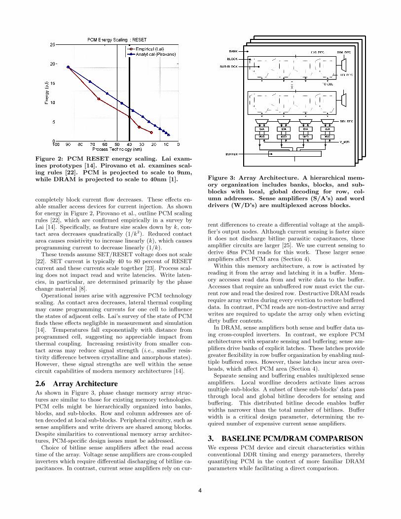
Figure 2: PCM RESET energy scaling. Lai exam-ines prototypes [14]. Pirovano et al. examines scal-ing rules [22]. PCM is projected to scale to 9nm,while DRAM is projected to scale to 40nm [1].
completely block current flow decreases. These effects en-able smaller access devices for current injection. As shownfor energy in Figure 2, Pirovano et al., outline PCM scalingrules [22], which are confirmed empirically in a survey byLai [14]. Specifically, as feature size scales down by k, con-tact area decreases quadratically (1/k2). Reduced contactarea causes resistivity to increase linearly (k), which causesprogramming current to decrease linearly (1/k).
These trends assume SET/RESET voltage does not scale[22]. SET current is typically 40 to 80 percent of RESETcurrent and these currents scale together [23]. Process scal-ing does not impact read and write latencies. Write laten-cies, in particular, are determined primarily by the phasechange material [8].
Operational issues arise with aggressive PCM technologyscaling. As contact area decreases, lateral thermal couplingmay cause programming currents for one cell to influencethe states of adjacent cells. Lai’s survey of the state of PCMfinds these effects negligible in measurement and simulation[14]. Temperatures fall exponentially with distance fromprogrammed cell, suggesting no appreciable impact fromthermal coupling. Increasing resistivity from smaller con-tact areas may reduce signal strength (i.e., smaller resis-tivity difference between crystalline and amorphous states).However, these signal strengths are well within the sensecircuit capabilities of modern memory architectures [14].
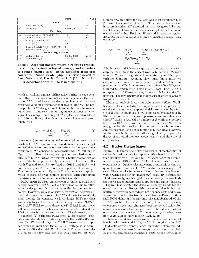
2.6 Array ArchitectureAs shown in Figure 3, phase change memory array struc-tures are similar to those for existing memory technologies.PCM cells might be hierarchically organized into banks,blocks, and sub-blocks. Row and column addresses are of-ten decoded at local sub-blocks. Peripheral circuitry, such assense amplifiers and write drivers are shared among blocks.Despite similarities to conventional memory array architec-tures, PCM-specific design issues must be addressed.
Choice of bitline sense amplifiers affect the read accesstime of the array. Voltage sense amplifiers are cross-coupledinverters which require differential discharging of bitline ca-pacitances. In contrast, current sense amplifiers rely on cur-
Figure 3: Array Architecture. A hierarchical mem-ory organization includes banks, blocks, and sub-blocks with local, global decoding for row, col-umn addresses. Sense amplifiers (S/A’s) and worddrivers (W/D’s) are multiplexed across blocks.
rent differences to create a differential voltage at the ampli-fier’s output nodes. Although current sensing is faster sinceit does not discharge bitline parasitic capacitances, theseamplifier circuits are larger [25]. We use current sensing toderive 48ns PCM reads for this work. These larger senseamplifiers affect PCM area (Section 4).
Within this memory architecture, a row is activated byreading it from the array and latching it in a buffer. Mem-ory accesses read data from and write data to the buffer.Accesses that require an unbuffered row must evict the cur-rent row and read the desired row. Destructive DRAM readsrequire array writes during every eviction to restore buffereddata. In contrast, PCM reads are non-destructive and arraywrites are required to update the array only when evictingdirty buffer contents.
In DRAM, sense amplifiers both sense and buffer data us-ing cross-coupled inverters. In contrast, we explore PCMarchitectures with separate sensing and buffering; sense am-plifiers drive banks of explicit latches. These latches providegreater flexibility in row buffer organization by enabling mul-tiple buffered rows. However, these latches incur area over-heads, which affect PCM area (Section 4).
Separate sensing and buffering enables multiplexed senseamplifiers. Local wordline decoders activate lines acrossmultiple sub-blocks. A subset of these sub-blocks’ data passthrough local and global bitline decoders for sensing andbuffering. This distributed bitline decode enables bufferwidths narrower than the total number of bitlines. Bufferwidth is a critical design parameter, determining the re-quired number of expensive current sense amplifiers.
3. BASELINE PCM/DRAM COMPARISONWe express PCM device and circuit characteristics withinconventional DDR timing and energy parameters, therebyquantifying PCM in the context of more familiar DRAMparameters while facilitating a direct comparison.
4

PCM DRAM
Delay & Timing
tRCD (cy) 22 5tCL (cy) 5 5tWL (cy) 4 4tCCD (cy) 4 4tWTR (cy) 3 3tWR (cy) 6 6tRTP (cy) 3 3tRP (cy) 60 5tRRDact (cy) 2 3tRRDpre (cy) 11 3
Energy
Array read (pJ/bit) 2.47 1.17Array write (pJ/bit) 16.82 0.39Buffer read (pJ/bit) 0.93 0.93Buffer write (pJ/bit) 1.02 1.02Background power (pJ/bit) 0.08 0.08
Table 2: Memory subsystem parameters.
3.1 Experimental MethodologyWe evaluate a four-core chip multiprocessor using the SESCsimulator [24]. The 4-way superscalar, out-of-order coresoperate at 4.0GHz. This datapath is supported by 32KB,direct-mapped instruction and 32KB, 4-way data L1 caches,which may be accessed in 2 to 3 cycles. A 4MB, 8-way L2cache with 64B lines is shared between the four cores andmay be accessed in 32 cycles.
Below the caches is a 400 MHz SDRAM memory subsys-tem modeled after Micron’s DDR2-800 technical specifica-tions [16]. We consider one channel, one rank, four x16 chipsper rank to achieve the standard 8B interface. Internally,each chip is organized into four banks to facilitate through-put as data are interleaved across banks and accessed in par-allel. We model a burst length of eight blocks. The memorycontroller has a 64-entry transaction queue.
We consider parallel workloads from the SPLASH-2 suite(fft, radix, ocean), SPEC OpenMP suite (art, equake, swim),and NAS parallel benchmarks (cg, is, mg) [3, 4, 27]. Eachapplication is simulated to completion. Regarding inputsets, we use 1M points for FFT, 514x514 grid for ocean,and 2M integers for radix. SPEC OpenMP workloads runMinneSpec-Large data set and NAS parallel benchmarks runwith Class A problem sizes. All applications are compiledusing gcc and Fortran compilers at the O3 optimization level.Particular applications in each benchmark suite are chosenfor their memory intensity. We did not consider a bench-mark if system performance or energy was not impacted byreplacing DRAM with PCM.
Delay and Timing. DDR defines its command inter-face with a series of timing constraints, which dictate whena command can issue. In Table 2, DRAM timing parame-ters are provided by Micron specifications [16] and analogousPCM timing parameters are derived from Table 1.
• tRCD specifies the delay between an array read andbuffer read/write command. This parameter is deter-mined by the 60ns array read latency, which includes48ns read (Table 1) and 7.5ns row decode [15]. At400MHz, tRCD for PCM is 22 cycles, 4.4x greater thanthe DRAM value of 5 cycles.
• tCL, tWL, tCCD, and tWTR constrain consecutive buffercommands and are independent of memory cell tech-nology. tWR, tRTP specify the delay between buffer
read/write commands and an array write of thatbuffered data. tWR, tRTP ensure data stability in thecross-coupled inverters that feed array write driversand are independent of memory cell technology.
• tRP specifies the delay between an array write and afollowing array read. Since an array read proceeds onlyafter previously buffered data is successfully writtenback to the array, tRP quantifies array write latency.The longer SET delay of 150ns determines PCM writelatency (Table 1) and tRP is 60 cycles at 400MHz.
• tRRDact, tRRDpre specify constraints on the frequencyof PCM array accesses to meet power budgets. Theparameters distinguish between array read (tRRDact)and write (tRRDpre) since a read is non-destructiveand a write is required only when a read evicts dirtybuffer contents. Furthermore, given asymmetric readand write energy costs, no single timing constraint cansatisfy both read and write power budgets. PCM readenergy and delay is 2.1x and 4.4x greater than that ofDRAM. Because power is energy divided by delay, aPCM read dissipates 0.47x the power of DRAM reads,which produces a tRRDact of 2 cycles (0.47x of 3 cycletRRD in DRAM). Similarly, tRRDpre is 11 cycles forPCM writes.
Thus, we estimate PCM read, write latencies are approxi-mately 4.4x, 12.0x greater than those for DRAM. PCM arrayreads may occur 2.1x more frequently and array writes mustoccur 3.6x less frequently than those for DRAM.
Energy. DRAM energy costs are calculated accordingto Micron technical notes and specifications [17]. However,these notes do not explicitly differentiate read and writeenergy since writes must follow every destructive DRAMread. A current diagram in the technical note indicates ar-ray read current is much greater than array write current.From this current diagram, we derive array write and readenergy costs, which are 25 and 75 percent of the total 1.56pJper DRAM bit.
From Table 1, PCM array reads consume 2.0 pJ of energyper bit. Furthermore, we use CACTI to estimate energyconsumed by peripheral circuitry to obtain approximately2.5pJ of total array read energy per bit [18]. Array writesconsume 13.5pJ or 19.2pJ when writing a zero or one. Onaverage, zeros and ones are equally likely and writes require16.35pJ of energy in addition to 0.53pJ peripheral circuitenergy. Thus, we derive PCM array read and write energies,which are 2.1x and 43.1x greater than those for DRAM.
Reads and writes to buffered data will consume similar en-ergy costs for PCM and DRAM since mechanisms for bufferaccess are independent of memory technology. Althoughvarious power modes exist for DRAM, in practice, we ob-serve only one power mode while an application executes;there are no opportunities to enter low power modes duringcomputation. This mode consumes 0.08pJ per buffered bitper memory cycle while clocks are enabled and memory isready to receive commands [17]. This background energyis consumed by peripheral circuitry common to both PCMand DRAM.
3.2 Evaluation: BaselineWe consider a PCM baseline architecture, which implementsDRAM-style buffering with a single 2048B-wide buffer. Fig-ure 4L illustrates end-to-end application performance when
5

Figure 4: Application delay and energy when using PCM as a DRAM replacement (L). With non-destructivePCM reads, only a fraction of reads first require a write for dirty data evicted from buffer (R).
PCM replaces DRAM as main memory. Application de-lay increases with penalties relative to DRAM ranging from1.2x (radix) to 2.2x (ocean, swim). On average, we observe a1.6x delay penalty. The energy penalties are larger, rangingfrom 1.4x (cg) to 3.4x (ocean), due to the highly expensivearray writes required when buffer contents are evicted. Onaverage, we observe a 2.2x energy penalty.
The end-to-end delay and energy penalties are more mod-est than the underlying technology parameters might sug-gest. Even memory intensive workloads mix memory ac-cesses with computation. Furthermore, the long latency,high energy array writes manifest themselves much less of-ten in PCM than in DRAM; non-destructive PCM reads donot require subsequent writes whereas destructive DRAMreads do. Figure 4R indicates only 28 percent of PCM arrayreads first require an array write of a dirty buffer.
To enable PCM for use below the lowest level processorcache in general-purpose systems, we must close the delayand energy gap between PCM and DRAM. Figure 4 indi-cates non-destructive PCM reads help mitigate underlyingdelay and energy disadvantages by default. We seek to elim-inate the remaining PCM-DRAM differences with architec-tural solutions. In particular, the baseline analysis considersa single 2048B-wide buffer per bank. Such wide buffering isinexpensive in DRAM, but incurs unnecessary energy costsin PCM given the expensive current injection required whenwriting buffer contents back into the array.
4. BUFFER ORGANIZATIONWe examine whether PCM subsystems can close the gapwith DRAM application performance and memory subsys-tem energy using area-neutral buffer reorganizations. To bea viable DRAM alternative, buffer organizations must hidelong PCM latencies, while minimizing PCM energy costs.Effective organizations would also mitigate PCM wear mech-anisms (Section 5).
To achieve area neutrality, we consider narrower buffersand additional buffer rows. The number of sense amplifiersdecreases linearly with buffer width, significantly reducingarea as fewer of these large circuits are required. We utilizethis area by implementing multiple rows with latches muchsmaller than the removed sense amplifiers. Narrow widths
reduce PCM write energy but negatively impact spatial lo-cality, opportunities for write coalescing, and applicationperformance. However, these penalties may be mitigatedby the additional buffer rows. We examine these fundamen-tal trade-offs by identifying designs that meet a DRAM-imposed area budget before optimizing delay and energy.
We consider buffer widths ranging from the original 2048Bto 64B, which is the line size of the lowest level cache. Weconsider buffer rows ranging from the original single rowto a maximum of 32 rows. At present, we consider a fullyassociative buffer and full associativity likely becomes in-tractable beyond 32 rows. Buffers with multiple rows usea least recently used (LRU) eviction policy implemented inthe memory controller.
4.1 Area and Density AnalysisWe estimate the net area impact of every buffer organi-zation, considering only array components affected by theorganization. Specifically, we consider the bitline periph-eral circuitry (e.g., sense amplifiers), additional decodingrequired by multiple buffer rows, and explicit latches. Weneglect area of components unrelated to the buffer, such aswordline decode.
Table 3 summarizes the parameters in our area model,which this section details. We consider area in units of tran-sistors (T) converted to square feature sizes (F 2), whichmakes our analysis independent of process technology.2 Weestimate the number of transistors in each circuit and es-timate transistor density using guidelines from Weste andHarris [26]. These guidelines differentiate between densedatapath circuits (e.g., 250 λ2/T) and sparse control cir-cuits (e.g., 1000 λ2/T). Datapaths operate on multi-bit datawords and perform the same function for every bit. As aresult, they consist of identical circuits repeated in one di-mension. In contrast, control circuits have less structureand, therefore, lower density.
DRAM Area Model. 8F 2 DRAM cells provide a suf-ficiently wide pitch to enable a folded bitline architecture,
2In a 90nm process, feature size F is 90nm and layout designλ = F/2 is 45nm. For example, a 14T sense amplifer im-plemented with a density of 250λ2/T occupies 3500λ2 area.Converting to F 2, each amplifier occupies 875F 2 area.
6
PCM DRAM
Array
A bank size (MB) 16 16C cell size (F 2) 9MLC, 12MLC 6
Periphery
S sense amplifer (T @ 250λ2/T) 44 14sense amplifer (F 2) 2750 875
L latch (T @ 250λ2/T) 8 0latch (F 2) 500 0
D decode 2-AND (T @ 1000λ2/T) 6 0decode 2-AND (F 2) 250 0
Buffer Organization
W buffer width (B) 64::2x::2048 2048R buffer rows (ea) 1::2x::32 1
Table 3: Area parameters where T refers to transis-tor counts, λ refers to layout density, and F 2 refersto square feature sizes. Sense amplifier transistorcount from Sinha et al. [25]. Transistor densitiesfrom Weste and Harris, Table 1.10 [26]. Notationi::j::k describes range of i to k in steps of j.
which is resilient against bitline noise during voltage sens-ing. However, since manufacturers often choose the den-sity of 6F 2 DRAM cells, we derive models using 6F 2 as aconservative point of reference that favors DRAM. The nar-row pitch in 6F 2 designs preclude folded bitlines, increasingvulnerability to noise and requiring unconventional array de-signs. For example, Samsung’s 6F 2 implements array blockswith 320 wordlines, which is not a power of two, to improvereliability [9].
AD = A·CD︸ ︷︷ ︸
array
+ WD·SD︸ ︷︷ ︸
sense
(1)
Equation (1) estimates array and sense amplifier area for the
baseline DRAM organization. AD defines the area budgetand PCM buffer organizations exceeding this budget are notconsidered. We consider a conservative DRAM cell size ofCD = 6F 2. Given the engineering effort required to opti-mize 6F 2 DRAM arrays, we expect a buffer reorganizationfor DRAM to be prohibitively expensive. Thus, the bufferwidth WD and rows RD are fixed at 2048B and 1; RD = 1does not impact AD and does not appear in Equation (1).This derivation uses a SD = 14T voltage sense amplifier,which consists of cross-coupled inverters with supportingtransistors for precharge and equalization [25].
PCM Area Model. As surveyed in Table 1, PCM cellsoccupy between 6-20F 2. Part of this spread is due to differ-ences in design and fabrication expertise for the new tech-nology. However, we also observe a correlation between cellsize and access device (e.g., the 6F 2 cell uses the relativelysmall diode). In contrast, we favor larger BJTs for theirlow access times. Cells with BJTs occupy between 9-12F 2.For 9-12F 2 PCM to be as dense as 6F 2 DRAM, multi-levelcells are necessary. Such cells have an effective density of4.5-6.0F 2 per bit, which we use for PCM cell area CP .
Equation (2) estimates PCM area AP from array, sense,latch, and decode contributions given buffer widths WP androws RP . We model a SP = 44T MLC current sense ampli-fier, which is larger than the SD = 14T voltage sense ampli-fier in the DRAM model [25]. A larger 22T current amplifieris necessary for low read times in PCM and two-bit MLC
requires two amplifiers for the least and most significant bits[5]. Amplifiers feed explicit LP =8T latches, which are twoinverters in series (4T) accessed via two pass gates (4T) thatselect the input from either the sense amplifier or the previ-ously latched value. Both amplifiers and latches are regulardatapath circuitry, capable of high transistor density (e.g.,250 λ2/T ).
AP = A·CP︸ ︷︷ ︸
array
+ WP ·SP︸ ︷︷ ︸
sense
+ RP ·WP ·LP︸ ︷︷ ︸
latch
+
RP ·G(log2R, 2)·DP︸ ︷︷ ︸
decode
(2)
A buffer with multiple rows requires a decoder to direct senseamplifier outputs to the correct row. A buffer with Rp rowsrequires Rp control signals each generated by an AND gatewith log2R inputs. Avoiding slow, large fan-in gates, wecompute the number of gates in an equivalent 2-AND im-plementation. G(n, k) computes the number of k-AND gatesrequired to implement a single n-AND gate. Each 2-ANDoccupies Dp = 6T area, arising from a 4T NAND and a 2Tinverter. The low density of decoders arise from its relativelyirregular tree structure.
This area analysis favors multiple narrow buffers. We il-lustrate with a qualitative example, which is supported byour detailed equations. Suppose widths are reduced by a fac-tor of R and the number of rows is increased by a factor of R.The width reduction means expensive sense amplifier area(2750F 2 each) is reduced by a factor of R while inexpensivelatches (500F 2 each) are increased by a factor of R. Givennegligible decoder overhead for modest R, such buffer reor-ganizations produce a net reduction in buffer area. However,we find these buffer reorganizations significantly impact thedegree of exploited memory access locality and the costs ofarray writes.
4.2 Buffer Design SpaceFigure 5 illustrates the delay and energy characteristics ofthe buffer design space for representative benchmarks. Thetriangles illustrate PCM and DRAM baselines, which imple-ment a single 2048B buffer. Circles illustrate various bufferorganizations. Open circles indicating organizations that re-quire less area than the DRAM baseline when using 12F 2
cells. Closed circles indicate additional designs that becomeviable when considering smaller 9F 2 cells. By default, thePCM baseline (green triangle) does not satisfy the area bud-get due to larger current sense amplifiers and explicit latches.
Figure 5L illustrates the delay and energy trends for theocean benchmark. Reorganizing a single, wide buffer intomultiple, narrow buffers reduces both energy costs and delay.Examining the Pareto frontier, we observe Pareto optimashift PCM delay and energy into the neighborhood of theDRAM baseline. Furthermore, among these Pareto optima,we observe a knee that minimizes both energy and delay. Forocean, this organization is four 512B-wide buffers. Such anorganization reduces the PCM delay, energy disadvantagesfrom 2.2x, 3.4x to more modest 1.2x, 1.05x.
These observations generalize to the average across allbenchmarks illustrated in Figure 5R. Although smaller 9F 2
PCM cells provide opportunities for wider buffers and ad-ditional rows, the associated energy costs are not justified.In general, diminishing marginal reductions in delay suggest
7

Figure 5: Pareto analysis for ocean (L) and benchmark average (R). Open circles indicate designs satisfyingarea constraints assuming 12F 2 PCM multi-level cells. Closed circles indicate additional designs satisfyingarea constraints assuming smaller 9F 2 PCM multi-level cells.
area savings from 9F 2 cells should go toward improving den-sity, not additional buffering.
Figure 6 illustrates memory subsystem effects from reor-ganized buffers averaged across all workloads. Although ourdesign space considers Rp up to 32 rows, we illustrate trendsup to Rp = 4 since we observe diminishing marginal delayand energy effects beyond Rp = 4. Figure 6UL illustratesthe number of array reads, which increases very slowly asbuffer width decreases exponentially from 2048B to 64B. Fora single row, a 32x reduction in buffer width produces only a2x increase in array reads, suggesting very little spatial local-ity within wide rows for the memory intensive workloads weconsider. The single row is evicted too quickly after its firstaccess, limiting opportunities for spatial reuse. However,we do observe significant temporal adaptivity. A 2048B-wide buffer with two rows requires 0.4x the array reads as a2048B-wide buffer with only a single row.
Figure 6UR illustrates increasing opportunities for writecoalescing, quantified by the number of array writes perbuffer write. As the number of rows in a 2048B-wide bufferincreases from one to two and four rows, array writes perbuffer write falls by 0.51x and 0.32x, respectively; the bufferscoalesce 49 and 68 percent of memory writes. Coalescingopportunities fall as buffer widths narrow beyond 256B. Re-garding 64B-wide buffers, since we use 64B lines in the low-est level cache, there are no coalescing opportunities fromspatial locality within a row buffered for a write. Increasingthe number of 64B rows has no impact since additional rowsexploit temporal locality, but any temporal locality in writesare already exploited by coalescing in the lowest level cache.
Figure 6LL illustrates delay trends. The delay trendsconfirm a lack of spatial locality within a row; row widthsmay be narrowed with little impact on application perfor-mance. Increasing the number of rows exploits temporallocality with great effect. The sensitivity of buffer width forRp > 1 suggests a temporal component to spatial reuse. Ifwe only buffer one row, that row is likely evicted by a bufferconflict before any spatial reuse. However, if we buffer mul-tiple rows, buffer conflicts decrease, opportunities for spatialreuse increase, and buffer width becomes more important.
Figure 6LR illustrates energy trends. We observe sub-
linear energy growth as we increase the number of rows. Forexample, energy costs for one and two rows are comparable.Although two rows consume twice the background energy,the second row significantly reduces the number of arrayreads/writes (Figure 6UL) and the effectiveness of write co-alescing in the buffer (Figure 6UR). These effects on arrayaccesses reduce dynamic energy much more rapidly than anyincrease in background energy. We observe near-linear en-ergy reductions as buffer width narrows since array read andwrite energy is directly proportional to width.
4.3 Evaluation: Buffer OrganizationOptimizing average delay and energy across the workloads,we find four 512B-wide buffers most effective. Figure 7Lillustrates the impact of reorganized PCM buffers. Delaypenalties are reduced from the original 1.60x to 1.16x. Thedelay impact ranges from 0.88x (swim) to 1.56x (fft) relativeto a DRAM-based system. Executing on effectively bufferedPCM, more than half the benchmarks achieve within 5 per-cent of their DRAM performance. Benchmarks that performless effectively exhibit low write coalescing rates. For exam-ple, buffers cannot coalesce any writes in the fft workload.
Buffering and write coalescing also reduces memory sub-system energy from the original 2.2x of Figure 4L to 1.0xparity with DRAM. Although each PCM array write re-quires 43.1x more energy than a DRAM array write, theseenergy costs are mitigated by narrow buffer widths and addi-tional rows, which reduce the granularity of buffer evictionsand expose opportunities for write coalescing, respectively.
Thus, we demonstrate area-neutral buffering that miti-gates fundamental PCM constraints and provide compet-itive performance and energy characteristics relative toDRAM-based systems. Narrow buffers mitigate high energyPCM writes and multiple rows to exploit locality. This local-ity not only improves performance, but also reduces energyby exposing additional opportunities for write coalescing.We evaluate PCM buffering using technology parameters at90nm. As PCM technology matures, baseline PCM laten-cies may improve. Moreover, process technology scaling willdrive linear reductions in PCM energy.
8
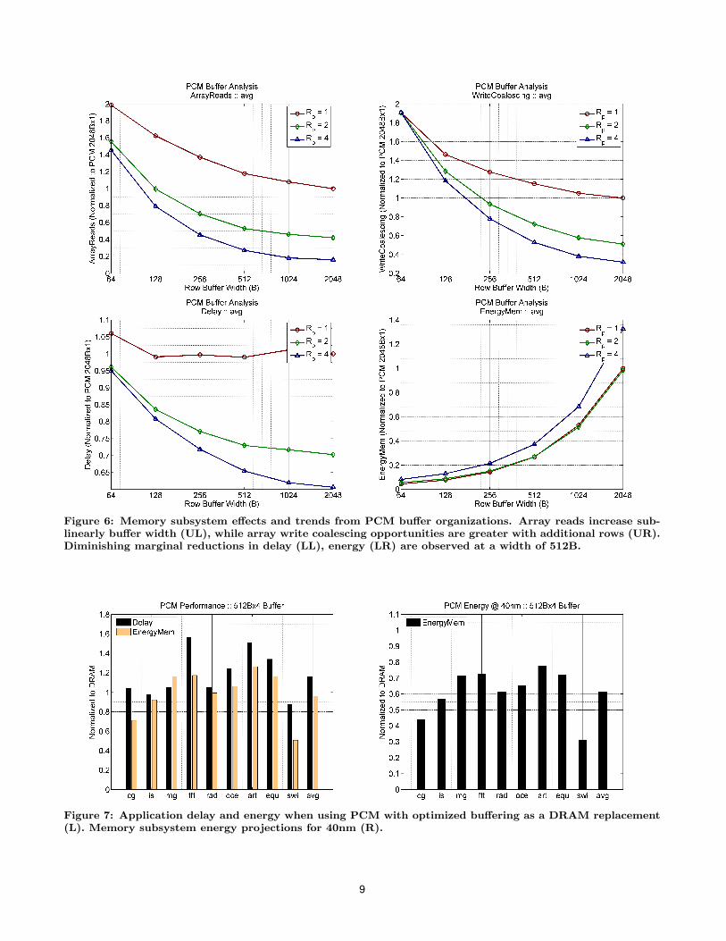
Figure 6: Memory subsystem effects and trends from PCM buffer organizations. Array reads increase sub-linearly buffer width (UL), while array write coalescing opportunities are greater with additional rows (UR).Diminishing marginal reductions in delay (LL), energy (LR) are observed at a width of 512B.
Figure 7: Application delay and energy when using PCM with optimized buffering as a DRAM replacement(L). Memory subsystem energy projections for 40nm (R).
9

4.4 Evaluation: Scaling ComparisonDRAM scaling faces many significant technical challengesas scaling attacks weaknesses in both components of theone transistor, one capacitor (1T1C) cell. Capacitor scal-ing is constrained by the DRAM storage mechanism, whichrequires maintaining charge on a capacitor. In future, pro-cess scaling is constrained by manufacturing small capacitorsthat store sufficient charge for reliably sensing despite largeparasitic capacitances on the bitline.
The scaling scenarios are also bleak for the access transis-tor. As this transistor scales down, increasing sub-thresholdleakage will make it increasingly difficult to ensure DRAMretention times. Not only is less charge stored in the ca-pacitor, that charge is stored less reliably. These trends im-pact the reliability and energy efficiency of DRAM in futureprocess technologies. According to ITRS, “manufacturablesolutions are not known” for DRAM beyond 40nm [1].
In contrast, ITRS projects PCM scaling mechanisms willextend to 9nm, after which other scaling mechanisms mightapply [1]. PCM scaling mechanisms have already beendemonstrated up to 20nm with a novel device structure fab-ricated by Raoux [23]. Although both DRAM and PCM areexpected to be viable at 40nm technologies, energy scalingtrends strongly favor PCM. Figure 2 projects a 2.4x reduc-tion in PCM energy from 80 to 40nm. In contrast, ITRSprojects DRAM energy falls by only 1.5x at 40nm [1], whichreflects the technical challenges of DRAM scaling.
Since PCM energy scales down 1.6x faster than DRAMenergy, PCM subsystems significantly outperforms DRAMsubsystems at 40nm. Figure 7R indicates PCM subsystemenergy is 61.3 percent that of DRAM averaged across work-loads. Switching from DRAM to PCM reduces energy costsby at least 22.1 percent (art) and by as much as 68.7 per-cent (swim). Note this analysis does not account for refreshenergy, which would further increase DRAM energy costs.Although ITRS projects constant retention time of 64msas DRAM scales to 40nm [1], less effective access transis-tor control may reduce retention times. If retention timesfall, DRAM refresh energy will increase as a fraction of totalDRAM energy costs.
5. PARTIAL WRITESIn addition to architecting PCM to offer competitive de-lay and energy characteristics relative to DRAM, we mustalso consider PCM wear mechanisms. To mitigate these ef-fects, we propose partial writes, which reduce the numberof writes to the PCM array by tracking dirty data from theL1 cache to the memory banks. This architectural solutionadds a modest amount of cache state to drastically reducethe number of bits written. We derive an analytical modelto estimate memory module lifetime from a combination offundamental PCM technology parameters and measured ap-plication characteristics. Partial writes, combined with aneffective buffer organization, increases memory module life-times to a degree that makes PCM below the lowest levelprocessor cache feasible.
5.1 MechanismPartial writes track data modifications, propagating this in-formation from the L1 cache down to the buffers at thememory banks. When a buffered row is evicted and writescontent to the PCM array, only modified data is written.
We consider partial writes at two granularities: lowest levelcache line size (64B) and word size (4B).
These granularities are least invasive since dirty wordsare tracked by store instructions from the microprocessorpipeline. In contrast, bit-level granularity requires knowl-edge of previous data values and expensive comparators.We analyze a conservative implementation of partial writes,which does not exploit cases where stores write the samedata values already stored. Detecting such cases would re-quire comparators.
Partial writes are supported by adding state to each cacheline, tracking stores using fine-grained dirty bits. At thedirty line granularity, 64B modifications are tracked begin-ning at the lowest level cache and requires only 1b per 64BL2 line. At the dirty word granularity, 4B modifications aretracked beginning at the L1 cache with 8b per 32B L1 lineand propagated to the L2 cache, which requires 16b per 64BL2 line. Overheads are 0.2 percent and 3.1 percent of eachcache line when tracking dirty lines and words, respectively.
When the L2 cache issues writebacks to memory, it mustcommunicate its state to the memory controller and acrossthe memory bus. Delay overheads for transmitting 16b ofstate is no more than one cycle in a DDR interface. Latchedat the addressed bank, this state controls pass gates placedbefore write drivers. Latched state for 64B and 4B partialwrites require WP RP /64 and WP RP /4 latches where WP isbuffer width and RP is the number of buffered rows. Thecost of pass gates for word drivers is WP ·2T .
Our buffer reorganizations achieve a net area savings,which accommodate these overheads. We reduce large senseamplifiers (2750F 2 each) by a factor of R and increase thenumber small latches (500F 2 each) by a factor of R. Partialwrites require a 3.1 percent latch overhead, increasing theeffective area cost for every latched bit (525F 2 each). How-ever, these overheads are dwarfed by area reductions fromusing narrower buffers and eliminating large sense amplifiers.
5.2 EnduranceEquation (3) estimates the lifetime of a memory moduledriven with access patterns observed in our memory inten-sive workloads. Table 4 summarizes the model parameters.The model estimates the number of writes per second Wfor any given bit. We first estimate memory bus occu-pancy, which has a theoretical peak command bandwidthof fm · (B/2)−1. Each command requires B/2 bus cycles totransmit its burst length B in a DDR interface, which pre-vents commands from issuing at memory bus speeds fm. Wethen scale this peak bandwidth by application-specific uti-lization. Utilization is computed by measuring the numberof memory operations Nw+Nr and calculating the processorcycles spent on these operations (B/2)·Mf . The processor isMf faster than fm. The time spent on memory operationsis divided by total execution time T .
W =fm
B/2·(Nw + Nr)·(B/2)·Mf
T︸ ︷︷ ︸
memBusOcc
×Nw
Nw + Nr︸ ︷︷ ︸
writeIntensity
×
8WP ·
(Nwa
Nwb
)
·δ
︸ ︷︷ ︸
bufferOrg
×1
C/2︸ ︷︷ ︸
capacity
(3)
10

Figure 8: PCM endurance with effective buffer organization (four 512B-wide buffers) and partial writes.
Endurance
W writes per second per bit calc
L memory module lifetime (s) calcE write endurance 1E+08
Memory Module
C logical capacity (Gb) 2Memory Bus Bandwidth
fm memory bus frequency (MHz) 400Mf processor frequency multiplier 10B burst length (blocks) 8
Application Characteristics
Nw, Nr number of writes, reads simT execution time (cy) sim
Buffer Characteristics
WP , RP buffer width (B), rows 512, 4Nwb, Nwa buffer, array writes simδ fraction of buffer written to array sim
Table 4: Endurance model parameters with simu-lated application-specific characteristics.
Since only a fraction of memory bus activity reaches thePCM to induce wear, we scale occupancy by write intensityto estimate the number of write operations arriving at therow buffers. In the worst case, the entire buffer must bewritten to the array. However, not all buffer writes causearray writes due to coalescing. Nwa/Nwb measures the coa-lescing effectiveness of the buffer, which filters writes to thearray. Lastly, partial writes mean only the dirty fraction δof a buffer’s 8WP bits are written to the array. Assumingeffective wear-leveling as done in Flash [13], writes will bespread across the C/2 physical bits in the module, which
is half the logical bits in two-bit multi-level PCM. Given Wwrites per second, a bit will fail in L = E/W seconds, whereE is the characterized endurance of PCM cells.
5.3 Evaluation: Partial WritesIn a baseline architecture with a single 2048B-wide buffer,average module lifetime is approximately 525 hours as calcu-lated by Equation (3). For our memory intensive workloads,we observe 32.8 percent memory bus utilization. Scaling byapplication-specific write intensity, we find 6.9 percent ofmemory bus cycles are utilized by writes. At the memorybanks, the single 2048B buffer provides limited opportunities
for write coalescing, eliminating only 2.3 percent of writesemerging from the memory bus. Frequent row replacementsin the single buffer limit opportunities for coalescing.
Figure 8 indicates significant endurance gains from reorga-nized buffers and partial writes. 64B and 4B partial writesimprove endurance to 0.7 and 5.6 years, respectively. Onaverage, the four 512B-wide buffers coalesce 38.9 percent ofwrites emerging from the memory bus, which is 47.0 percentutilized. Writes alone utilize 11.0 percent of the bus. Buffersuse partial writes so that only a fraction of the buffer’s bitsis written to the array. As shown in Figure 9, only 59.3 and7.6 percent of the buffer must be written to the array for64B and 4B partial writes.
Considering only memory intensive workloads, this anal-ysis is conservative. PCM subsystems would more likely ex-perience a mix of compute and memory intensive workloads.Expected lifetimes would be higher had we considered, forexample, single-threaded SPEC integer workloads. How-ever, such workloads are less relevant for a study of memorysubsystems. Moreover, within memory intensive workloads,we would expect to see a mix of read and write intensiveapplications, which may further increase lifetimes.
Endurance might be further improved by using single-levelinstead of multi-level cells. This would improve the expectedlifetime since more physical bits deliver the same numberof logical bits. Endurance would also benefit from morefine-grained partial writes. Partial bit writes would requireadditional overheads for shadow buffers to track previousdata values and comparators to determine the difference,improving endurance at the cost of density.
Scalability is projected to improve PCM endurance fromthe current 1E+08 writes per bit to 1E+12 writes per bit at32nm with known manufacturable solutions [1]. This higherendurance increases lifetime by four orders of magnitude inour models. ITRS also anticipates 1E+15 PCM writes at22nm although the source of these projections is less clearsince manufacturable solutions are currently unknown.
6. CONCLUSIONWe provide a rigorous survey and derivation of phase
change memory properties to drive architectural studies andenhancements. Architecturally relevant parameters are ex-pressed within a DDR framework to facilitate a DRAM com-
11

Figure 9: Partial writes and fraction of dirty datain four 512B-wide buffers.
parison. This comparison found that PCM’s long latencies,high energy, and finite endurance can be effectively miti-gated. Effective buffer organizations and partial writes makePCM competitive with DRAM at current technology nodes.Moreover, these complexity effective solutions are area neu-tral, a critical constraint in memory manufacturing.
The proposed memory architecture lays the foundationfor exploiting PCM scalability and non-volatility in mainmemory. PCM scalability implies lower main memory en-ergy and greater write endurance. Furthermore, non-volatilemain memories will fundamentally change the landscape ofcomputing. Software cognizant of this newly provided per-sistance can provide qualitatively new capabilities. For ex-ample, system boot/hibernate will be perceived as instan-taneous; application checkpointing will be inexpensive; filesystems will provide stronger safety guarantees. Thus, theanalysis in this work is a step towards a fundamentallynew memory hierarchy with deep implications across thehardware-software interface.
7. REFERENCES
[1] Process integration, devices & structures.International Technology Roadmap forSemiconductors, 2007.
[2] S. Ahn et al. Highly manufacturable high densityphase change memory of 64Mb and beyond. InInternational Electron Devices Meeting, 2004.
[3] V. Aslot and R. Eigenmann. Quantitativeperformance analysis of the SPEC OMPM2001benchmarks. Scientific Programming, 11(2), 2003.
[4] D. Bailey et al. NAS parallel benchmarks. In TechnicalReport RNR-94-007, NASA Ames Research Center,March 1994.
[5] M. Bauer et al. A multilevel-cell 32mb flash memory.In International Solid-State Circuits Conference, 1995.
[6] F. Bedeschi et al. An 8Mb demonstrator forhigh-density 1.8V phase-change memories. InSymposium on VLSI Circuits, 2004.
[7] F. Bedeschi et al. A multi-level-cell bipolar-selectedphase-change memory. In International Solid-StateCircuits Conference, 2008.
[8] Y. Chen et al. Ultra-thin phase-change bridge memorydevice using GeSb. In International Electron DevicesMeeting, 2006.
[9] Y. Choi. Under the hood: DRAM architectures: 8F2vs. 6F2. EE Times, February 2008.
[10] R. Hamming. Error detecting and error correctingcodes. Bell System Technical Journal, 29(2), April1950.
[11] H. Horii et al. A novel cell technology using N-dopedGeSbTe films for phase change RAM. In Symposiumon VLSI Technology, 2003.
[12] S. Kang et al. A 0.1um 1.8V 256Mb 66MHzsynchronous burst PRAM. In International Solid-StateCircuits Conference, 2006.
[13] T. Kgil and T. Mudge. FlashCache: A NAND flashmemory file cache for low power web servers. InInternational Conference on Compilers on Compilers,Architecture, and Synthesis for Embedded Systems,October 2006.
[14] S. Lai. Current status of the phase change memoryand its future. In International Electron DevicesMeeting, 2003.
[15] K.-J. Lee et al. A 90nm 1.8V 512Mb diode-switchPRAM with 266 MB/s read throughput. Journal ofSolid-State Circuits, 43(1), January 2008.
[16] Micron. 512Mb DDR2 SDRAM component data sheet:MT47H128M4B6-25. In www.micron.com, March 2006.
[17] Micron. Technical note TN-47-04: Calculatingmemory system power for DDR2. In www.micron.com,June 2006.
[18] N. Muralimanohar et al. Optimizing NUCAorganizations and wiring alternatives for large cacheswith CACTI 6.0. In International Symposium onMicroarchitecture, December 2007.
[19] T. Nirschl et al. Write strategies for 2 and 4-bitmulti-level phase-change memory. In InternationalElectron Devices Meeting, 2008.
[20] H. Oh et al. Enhanced write performance of a 64mbphase-change random access memory. In InternationalSolid-State Circuits Conference, 2005.
[21] F. Pellizzer et al. A 90nm phase change memorytechnology for stand-alone non-volatile memoryapplications. In Symposium on VLSI Circuits, 2006.
[22] A. Pirovano et al. Scaling analysis of phase-changememory technology. In International Electron DevicesMeeting, 2003.
[23] S. Raoux et al. Phase-change random access memory:A scalable technology. IBM Journal of Research andDevelopment, 52(4/5), Jul/Sept 2008.
[24] J. Renau et al. SESC simulator. Inhttp://sesc.sourceforge.net, 2005.
[25] M. Sinha et al. High-performance and low-voltagesense-amplifier techniques for sub-90nm sram. InInternational Systems-on-Chip Conference, 2003.
[26] N. Weste and D. Harris. CMOS VLSI Design. PearsonEducation, 3 edition, 2005.
[27] S. Woo et al. The SPLASH-2 programs:Characterization and methodological considerations.In International Symposium on ComputerArchitecture, June 1995.
12