architectural optimization for performance- and...
TRANSCRIPT

Architectural Optimization for Performance- and
Energy-Constrained Sensor Processors
by
Leyla Nazhandali
A dissertation proposal submitted in partial fulfillmentof the requirements for the degree of
Doctorate of Philosophy(Computer Science and Engineering)
in The University of Michigan2006
Doctoral Committee:
Associate Professor Todd M. Austin, ChairProfessor Trevor N. MudgeAssociate Professor David BlaauwAssistant Professor Dennis Michael Sylvester

c© Leyla Nazhandali 2006All Rights Reserved

To my parents, Hadi and Azam
and to my husband, Masoud
ii

ACKNOWLEDGEMENTS
I would first like to thank my outstanding advisor, Professor Todd Austin, for his con-
tinuous guidance, strong support and encouragement without which, this work would have
not been possible. It has been truly a privilege for me to work with him and I look forward
to our further corporations in the future.
I also thank my dissertation committee, Prof. Trevor Mudge, Prof. David Blaauw, and
Prof. Dennis Sylvester for their support and feedback.
I would like to acknowledge breadth and depth of help I have received from my friends
at the Advanced Computer Architecture Laboratory at The University of Michigan. In
particular, the spirit of perseverance and cooperation in the Subliminal Project Group, led
by Prof. Todd Austin and Prof. David Blaauw, has produced a unique opportunity that
nurtures academic excellence.
My sincere gratitude goes to my Iranian friends whose kindness and support made
me feel at home, while living thousands of miles away from home. Finally, I would like to
express my eternal and deep gratitude to my parents whose endless love has been the engine
which has driven me throughout my life, including this endeavor; and to my husband,
Masoud Agah, without whom life would have been empty.
iii

TABLE OF CONTENTS
DEDICATION . . . . . . . . . . . . . . . . . . . . . . . . . . . . . . . . . . . . . ii
ACKNOWLEDGEMENTS . . . . . . . . . . . . . . . . . . . . . . . . . . . . . . iii
LIST OF FIGURES . . . . . . . . . . . . . . . . . . . . . . . . . . . . . . . . . . vi
LIST OF TABLES . . . . . . . . . . . . . . . . . . . . . . . . . . . . . . . . . . . viii
LIST OF APPENDICES . . . . . . . . . . . . . . . . . . . . . . . . . . . . . . . ix
CHAPTERS
1 Introduction . . . . . . . . . . . . . . . . . . . . . . . . . . . . . . . . . 11.1 Sensor Processing . . . . . . . . . . . . . . . . . . . . . . . . . . 31.2 Related Work . . . . . . . . . . . . . . . . . . . . . . . . . . . . 8
1.2.1 Clever Dust 1 and 2 . . . . . . . . . . . . . . . . . . . . . 81.2.2 SNAP/LE . . . . . . . . . . . . . . . . . . . . . . . . . . 91.2.3 Hempstead et. al. Processor . . . . . . . . . . . . . . . . . 10
1.3 Thesis Organization . . . . . . . . . . . . . . . . . . . . . . . . . 11
2 Subthreshold-Voltage Circuit Design . . . . . . . . . . . . . . . . . . . . 142.1 Subthreshold-Voltage Circuit Operation . . . . . . . . . . . . . . 152.2 Architectural Energy Optimization . . . . . . . . . . . . . . . . . 17
3 Architectural Trade-off Analyses at Subthreshold Voltages . . . . . . . . . 223.1 ISA Optimizations . . . . . . . . . . . . . . . . . . . . . . . . . . 223.2 Experimental Framework . . . . . . . . . . . . . . . . . . . . . . 263.3 Microarchitectural Design Space Analysis . . . . . . . . . . . . . 273.4 Summary and Insights . . . . . . . . . . . . . . . . . . . . . . . . 32
4 An Extremely Energy-Efficient Sensor Processor Architecture with Com-pact 12-Bit RISC ISA . . . . . . . . . . . . . . . . . . . . . . . . . . . . 34
4.1 Instruction Set Architecture Optimizations . . . . . . . . . . . . . 36
iv

4.1.1 RISC Encoding . . . . . . . . . . . . . . . . . . . . . . . 364.1.2 Two-Operand Format with Memory Operands . . . . . . . 374.1.3 Micro-operations . . . . . . . . . . . . . . . . . . . . . . 394.1.4 Application-Specific Instructions . . . . . . . . . . . . . . 394.1.5 Code Density Analysis . . . . . . . . . . . . . . . . . . . 40
4.2 Application-Driven Memory Optimizations . . . . . . . . . . . . 414.3 Microarchitectural Optimizations . . . . . . . . . . . . . . . . . . 43
4.3.1 Out-of-Order Execution . . . . . . . . . . . . . . . . . . . 454.3.2 Taken Branch Speculation . . . . . . . . . . . . . . . . . 45
4.4 Energy-Performance Analysis . . . . . . . . . . . . . . . . . . . . 464.4.1 Experimental Framework . . . . . . . . . . . . . . . . . . 464.4.2 Simulated Results . . . . . . . . . . . . . . . . . . . . . . 47
4.5 Summary and Insights . . . . . . . . . . . . . . . . . . . . . . . . 50
5 Prototype Physical Design . . . . . . . . . . . . . . . . . . . . . . . . . . 53
6 Accurate Evaluation of Sensor Processors . . . . . . . . . . . . . . . . . . 626.1 Current Sensor Processors’ Evaluations . . . . . . . . . . . . . . . 636.2 Proposed Workload . . . . . . . . . . . . . . . . . . . . . . . . . 65
6.2.1 Application Building Blocks . . . . . . . . . . . . . . . . 656.2.2 Application Compositions . . . . . . . . . . . . . . . . . 68
6.3 Metrics . . . . . . . . . . . . . . . . . . . . . . . . . . . . . . . . 736.4 Summary and Insights . . . . . . . . . . . . . . . . . . . . . . . . 77
7 Conclusions and Future Directions . . . . . . . . . . . . . . . . . . . . . . 807.1 Summary of Contributions . . . . . . . . . . . . . . . . . . . . . 807.2 Future Directions . . . . . . . . . . . . . . . . . . . . . . . . . . 82
APPENDICES . . . . . . . . . . . . . . . . . . . . . . . . . . . . . . . . . . . . . 83
BIBLIOGRAPHY . . . . . . . . . . . . . . . . . . . . . . . . . . . . . . . . . . . 106
v

LIST OF FIGURES
Figure1.1 Computing Systems’ Fast Track of Size Scaling . . . . . . . . . . . . . . . 21.2 Sensor Processors’ Several Components . . . . . . . . . . . . . . . . . . . 31.3 Sensor Processor Applications . . . . . . . . . . . . . . . . . . . . . . . . 41.4 Performance of Sensor Processor Applications on Embedded Targets . . . . 61.5 Clever Dust 2 Architecture [26] . . . . . . . . . . . . . . . . . . . . . . . . 91.6 SNAP Architecture [14]. . . . . . . . . . . . . . . . . . . . . . . . . . . . 101.7 Hempstead et.al. Architecture [17]. . . . . . . . . . . . . . . . . . . . . . . 112.1 Inverter at Subthreshold Voltage. . . . . . . . . . . . . . . . . . . . . . . . 162.2 Energy as a Function of Voltage . . . . . . . . . . . . . . . . . . . . . . . 192.3 Energy-Optimal Operating Points . . . . . . . . . . . . . . . . . . . . . . 203.1 Logic vs. Memory Energy Trade-off . . . . . . . . . . . . . . . . . . . . . 233.2 Impact of ISA Optimization on Code Size and Control Logic Complexity . 253.3 First-Generation Sensor Processor Microarchitecture Overview. . . . . . . 283.4 Processor Energy vs. Performance . . . . . . . . . . . . . . . . . . . . . . 293.5 Energy Demand vs. Voltage . . . . . . . . . . . . . . . . . . . . . . . . . 314.1 ISA Organization. . . . . . . . . . . . . . . . . . . . . . . . . . . . . . . 374.2 Code Density Analysis. . . . . . . . . . . . . . . . . . . . . . . . . . . . 414.3 Data Memory Pre-decode Architecture. . . . . . . . . . . . . . . . . . . . 424.4 Instruction Pre-decode Architecture. . . . . . . . . . . . . . . . . . . . . . 434.5 Microarchitectural Organization. . . . . . . . . . . . . . . . . . . . . . . 444.6 Limited Out-of-Order Execution. . . . . . . . . . . . . . . . . . . . . . . 454.7 Pareto Analysis of First and Second-Generation Designs. . . . . . . . . . . 474.8 CPI andVmin Correlation . . . . . . . . . . . . . . . . . . . . . . . . . . . 494.9 Energy Distribution of the Base Processor at Two Different Voltages . . . . 505.1 Subthreshold-Voltage Sensor Processor Test Chip Layout . . . . . . . . . . 545.2 Subthreshold-Voltage Sensor Processor Test Chip Die Photo . . . . . . . . 555.3 Fabricated Processor Core Architecture . . . . . . . . . . . . . . . . . . . 55
vi

5.4 Fabricated SRAM Design . . . . . . . . . . . . . . . . . . . . . . . . . . . 565.5 Level Converter Design . . . . . . . . . . . . . . . . . . . . . . . . . . . . 565.6 Processor Core Frequency w.r.t. Supply Voltage for Several Tested Chips . 575.7 The Active and Leakage Energy Consumption of the Processor . . . . . . 585.8 The Energy Consumption of Processor Core and the Memory . . . . . . . . 585.9 Measured Operating Frequency of 26 Chips at Three Different Voltages . . 595.10 Emin andVmin Distribution over 26 Chips . . . . . . . . . . . . . . . . . . 595.11 Subthreshold-Voltage Sensor Processor Test Chip Die Photo . . . . . . . . 605.12 Energy Consumption of the Processor Core for Several Applications . . . . 605.13 Pareto Analysis of Several Sensor Processors . . . . . . . . . . . . . . . . 616.1 General View of an Application Composition. . . . . . . . . . . . . . . . . 696.2 Secure Composition. . . . . . . . . . . . . . . . . . . . . . . . . . . . . . 696.3 Reliable Composition. . . . . . . . . . . . . . . . . . . . . . . . . . . . . 706.4 Stats Composition. . . . . . . . . . . . . . . . . . . . . . . . . . . . . . . 706.5 Catalog Composition. . . . . . . . . . . . . . . . . . . . . . . . . . . . . . 706.6 Detect Composition. . . . . . . . . . . . . . . . . . . . . . . . . . . . . . 716.7 Query Composition. . . . . . . . . . . . . . . . . . . . . . . . . . . . . . . 716.8 RLE stream Composition. . . . . . . . . . . . . . . . . . . . . . . . . . . 726.9 Diff stream Composition. . . . . . . . . . . . . . . . . . . . . . . . . . . . 726.10 AODV route Composition. . . . . . . . . . . . . . . . . . . . . . . . . . . 726.11 Simpleroute Composition. . . . . . . . . . . . . . . . . . . . . . . . . . . 736.12 EPB Representation . . . . . . . . . . . . . . . . . . . . . . . . . . . . . . 736.13 xRT Representation . . . . . . . . . . . . . . . . . . . . . . . . . . . . . . 746.14 Relative Energy Consumption of the Core and Memory . . . . . . . . . . . 756.15 Composition Footprint Comparison . . . . . . . . . . . . . . . . . . . . . 766.16 Pareto Analysis of Several Subliminal Processors . . . . . . . . . . . . . . 77
vii

LIST OF TABLES
Table1.1 Sensor Processing Algorithms . . . . . . . . . . . . . . . . . . . . . . . . 51.2 Sensor Processing Data Rates . . . . . . . . . . . . . . . . . . . . . . . . . 133.1 First-Generation Sensor Processor Instruction Set Summary . . . . . . . . 246.1 Application Building Block Categories. . . . . . . . . . . . . . . . . . . . 65A.1 Data Alignment in Memory . . . . . . . . . . . . . . . . . . . . . . . . . . 85A.2 Addressing Mode Summary . . . . . . . . . . . . . . . . . . . . . . . . . 87A.3 Shift Directions . . . . . . . . . . . . . . . . . . . . . . . . . . . . . . . . 89A.4 Addressing Mode Summary for Shift Instructions . . . . . . . . . . . . . . 89A.5 Short Immediate Data . . . . . . . . . . . . . . . . . . . . . . . . . . . . . 89A.6 Operand Encoding . . . . . . . . . . . . . . . . . . . . . . . . . . . . . . 90A.7 Memory Index Bits . . . . . . . . . . . . . . . . . . . . . . . . . . . . . . 91A.8 Different Modes of Operation for Address Instruction . . . . . . . . . . . . 92A.9 Routine Mode Summary . . . . . . . . . . . . . . . . . . . . . . . . . . . 93A.10 Jump Condition Summary . . . . . . . . . . . . . . . . . . . . . . . . . . 93B.1 Second-Generation ISA Encoding . . . . . . . . . . . . . . . . . . . . . . 95B.2 Second-Generation ISA Mnemonic Description . . . . . . . . . . . . . . . 96
viii

LIST OF APPENDICES
APPENDIXA First-Generation Subliminal ISA Documentation . . . . . . . . . . . . . . 84B Second-Generation Subliminal ISA Encoding . . . . . . . . . . . . . . . . 95C Selective Developed Applications in First-Generation
Subliminal Assembly Language . . . . . . . . . . . . . . . . . . . . . . . 97
ix

CHAPTER 1
Introduction
The size scaling trends in computer design have seen supercomputers shrink into mini-
computers, then desktops, then handhelds, and most recently into sensor processors. With
each reduction in size, systems have enjoyed decreased cost and power requirements and
new computing applications. Sensor processors represent a new level of compact and
portable computing. These small processing systems reside in the environment they mon-
itor, combining sensing, computation, storage, communication, and power supplies into
small form-factors [18, 25]. Sensor processors encompass a vast array of applications,
ranging from medical monitoring, to environmental sensing, to industrial inspection, and
military surveillance [15].
Sensor platforms carry with them a number of form-factor requirements that place
heavy constraints on the energy available for computation [23, 25]. First, many appli-
cations require a sensor node that is very small in size. For example, an eyeball activity
monitor must be small enough to be embedded into the epidermis of the eyeball. Second,
sensor processors must carry their energy supplies within this small form-factor, in the form
of batteries or apparatus appropriate to scavenge energy, such as a solar cell. In either case,
the quantity of energy available to sensor application processing is quite limited. For ex-
ample, a 2g vanadium oxide battery contains 720 mA-hr of energy, enough to power ARM,
1

Figure 1.1: Computing Systems’ Fast Track of Size Scaling
Ltd’s most energy-efficient ARM 720T processor at 100MHz for 45 hrs [1]. Certainly, this
energy payload is not sufficient for long-term sensing applications, such as a heart monitor
for which installation requires surgery.
Fortunately, the energy demands of sensor processing platforms are mitigated by their
modest processing demands [14, 20]. For example, a blood pressure monitor sensor re-
quires a sensing capability of approximately 800 bps. Passing the sensing data to a software-
based digital threshold monitor, which watches for high or low blood pressure events,
would require about 10,000 instructions per second processing power. Higher-rate nat-
ural data streams, such as electrical signals from the human brain, are generated at data
rates of about 3,200 bps. Even these higher-rate signals could be processed by a digital
filter, analyzed with a threshold monitor and compressed for storage with less than 56,000
instructions per second. Given the low computational demands of many sensor process-
ing applications, there is a significant opportunity to reduce processing energy demands
through low-frequency, low-voltage designs.
In this chapter, we set the stage for the design and evaluation of sensor processors by
looking at the sensor processing characteristics and the related work.
2

Figure 1.2: Sensor Processors’ Several Components
1.1 Sensor Processing
To effectively gauge the processing and energy demands of sensor processors, we must
first assemble a sensor processing benchmark collection and examine the microprocessors’
performance under a variety of sensor processing data streams. Table 1.1 lists the sen-
sor processing benchmarks that we examine in this study. The applications are divided
into three categories: communication algorithms, computational processing, and sensing
algorithms. These programs represent a broad slice of the types of applications one could
expect to see on an ultra-low energy sensor processor platform.
In the communication domain,adRoutrepresents a simple routing routine for an ad-
hoc sensor communication network (similar to [24]). The algorithm accepts packets from
nearby nodes and, based on whether or not the destination node is closer or further away
from the sender node, the algorithm determines if each packet should be dropped or be
3

Figure 1.3: Sensor Processor Applications
re-sent. ThecompRLE[5] represents a low-overhead compression algorithm, which is typ-
ically applied to data packets before transmission.TEA [27]is a 128-bit strong encryption
algorithm, similar to what would be used in secure sensing applications. Finally,crc8 cal-
culates an 8-bit checksum for a 24-bit piece of data, appending the checksum to the end of
the data to produce a 32-bit value. This particular CRC can detect up to eight consecutive
wrong bits. In the computation processing domain, we have integer multiply and integer
divide algorithms. The computational workload also includes insertion sort and binary
search algorithms that have many possible uses in sensor applications. For example, sort-
ing is used in sensing applications where the top-N samples are tabulated. In the sensing
domain, we have data averaging and filtering algorithms in addition to a Schmidt trigger
threshold detector designed to spot events where data values fall below or above a specified
4

Table 1.1: Sensor Processing Algorithms
Description Application Code Sizenibble
Communication Algorithms
adRout Ad-hoc router control algorithm 42
compRLE Run-length encoded compressor 73
TEA TEA encryption algorithm 85
crc8 Cyclic redundancy code generator99
Computational Processing
divide Unsigned integer division 80
multiply Unsigned multiplication 48
inSort In-place insertion sort 78
binSearch Binary search 90
Sensing Algorithms
intAVG Signed integer average 113
intFilt 4-tap signed FIR filter 106
tHold Digital threshold detector 45
threshold (with a hysteresis).
Sensor processor platforms evaluate environmental information in real-time, by read-
ing, processing, compressing, storing, and eventually transmitting the information to in-
terested parties. To better understand the computational demands of a real-time sensor
processor platform, we tabulated the data processing rates of a variety of phenomena. Ta-
ble 1.2 lists a number of applications and their associated sample rates (in Hz, samples per
second) and the sample precision (in bits per sample). These data rates were gathered from
a variety of sources, including [10, 9, 13]. We have divided the applications intolow-, mid-
andhigh-bandwidth rates, which reflect sample rates of less than 100 Hz, 100 – 1 kHz, and
greater than 1 kHz, respectively.
5

0.0000010.000010.00010.0010.010.1
110
1001000
10000100000
ARM 720T@ 1.2V,100 MHz
ARM7TDMI @1.2V, 133
MHz
ARM 920T@ 1.2V,250 MHz
ARM1020T @1.2V, 325
MHz
best-proposed@ 1.2V,114 MHz
best-proposed@ 0.5V, 9
MHz
best-proposed@ 0.232V,
168 kHz
Low - xRT Mid - xRT High - xRT
Figure 1.4: Performance of Sensor Processor Applications on Embedded Targets -xRTratings for four commercial processors and an energy-efficient design proposed in this workat three different voltages with respect to low-, mid- and high-bandwidth requirements.The performance metricxRT indicates how many times faster than real-time a processorperforms.
Figure 1.4 illustrates the performance of four commercial embedded processors, in ad-
dition to one energy-efficient sensor processor design proposed in this thesis at three differ-
ent voltages. Each of the processors are implemented in a 0.13µm IBM process. For each
processor we show thexRTrating, which is computed via simulation by determining how
many times faster than real-time the processor can handle the worst-case data stream rate
on the most computationally intensive sensor benchmark. For example, the ARM 720T at
1.2V with a 100 MHz clock is able to process worst-case mid-bandwidth data 2965 times
faster than real-time data rates.
A few of the high-bandwidth sensor applications can be served by the commercial ARM
processors, while the highest bandwidth A/D sample rate greatly exceeds the computation
capability of even the most competent embedded processors. Consequently, we restrict our
studies in this work to the lesser demands of the low- and mid-bandwidth sensor processing
applications. It is clear from Figure 1.4 that the low- and mid-bandwidth sensor process-
6

ing applications have computational demands that are well below those delivered by the
commercial ARM processors. The same is true for the energy-efficient proposed design at
full-voltage (1.2V) and 114 MHz. This design services the mid-bandwidth applications at
more than 2,253 times the required worst-case processing requirement.
We can reduce the energy demands of these applications by reducing the frequency
of the processor which, in turn, accommodates reductions in the voltage. As voltage is
lowered, energy demands decrease quadratically. However, even the lowest superthreshold
voltages still deliver too much performance. The energy-efficient proposed design is shown
in Figure 1.4 at 0.5V (i.e., the lowest superthreshold voltage accommodated by the IBM
process technology). Even this low-voltage design is capable of delivering 180 times the
performance required by the mid-range sensor processing applications.
To further reduce energy requirements, we must consider running our sensor proces-
sors at subthreshold voltages. At subthreshold voltages the processor will operate with a
Vdd below that ofVth, resulting in a significant energy reduction with a great impact on
performance. The energy-efficient subthreshold design in Figure 1.4 delivers more than 4
times the desired performance for mid-bandwidth applications at 232 mV with a 168kHz
clock. Running this design any slower would require additional energy – why this is the
case, we expound in the following chapter.
It is noteworthy to mention that even increasing the sleep time of the processors is not
helpful in reducing the energy per instruction. The run-and-sleep technique, in which the
processor runs to execute a job and goes to sleep when the job is finished, reduces the
overall energy consumption of a processor because it saves the energy consumed in idle
state. However, in our analysis we are considering energy per instruction; hence, we do not
include the idle energy consumption. In other words, we are making a comparison between
the energy consumption of the processors during their service time, and we assume that
they all employ some technique to save energy in idle periods.
7

1.2 Related Work
Although numerous studies have been done in the area of sensor network system de-
sign, research on energy-efficient sensor processors is fairly new and the number of studies
on this topic is limited. Most sensor network testbeds [18, 25, 6] use off-the-shelf micro-
controllers such as such as the 8-bit ATMega128L, operating between 4MHz and 8MHz
and consuming about 1.5nJ/instruction (more than three orders of magnitude more energy
than the processors studied in this work). Some of the high-end sensor network platforms
[7, 3] use Intel StrongARM/XScale processor, consuming 1nJ/instruction.
Burd et al., presented some of the early work on energy-efficient processor designs
in [11]. They acknowledge the fact that prior to their work, traditional architectural design
methodologies for microprocessor systems had focused primarily on performance, with en-
ergy consumption being an afterthought. They demonstrated a top-down processor system
design methodology for reducing energy consumption, with the performance requirements
of portable devices being the focus. However, their study is mostly concentrated on circuit-
level optimizations with little focus on the processor core architecture.
In the sensor processing domain, we review the following three major projects: Clever
Dust, SNAP/LE and, Hempstead et. al. processor.
1.2.1 Clever Dust 1 and 2
Clever Dust 1 and 2 [26], developed as part of the Smart Dust project at UC-Berkeley,
are two 8-bit RISC microcontrollers specifically designed for Dust sensor motes with the
objective of reducing energy consumption. Clever Dust 2, inspired by the low-power Cool-
RISC microprocessor, is a load-store RISC Harvard architecture with no pipelining. It re-
portedly consumes 12pJ per instruction to execute general instructions excluding memory
operations and the energy consumption for instruction fetch.
8

Figure 1.5: Clever Dust 2 Architecture [26]
1.2.2 SNAP/LE
SNAP/LE [14] is a sensor network processor based on an asynchronous, data-driven,
RISC core with a low-power idle state and low-wakeup latency. SNAP/LE has an in-order,
single-issue core that does not perform any speculation. It has a 16-bit datapath consuming
24pJ per instruction.
9

Figure 1.6: SNAP Architecture [14].
1.2.3 Hempstead et. al. Processor
Hempstead, et. al. [17] present an application-driven architecture which off-loads im-
mediate event handling from the general purpose computing component and leaves it idle
in order to lower the power consumption of the system. With a 10% duty cycle (i.e. system
being idle 90% of the time), this system consumes 2W at 100kHz, which, assuming a CPI
of 1, results in about 20pJ per instruction.
10

Figure 1.7: Hempstead et.al. Architecture [17].
The vast majority of work in sensor processor design has been concentrated on super-
threshold voltages, resulting in higher energy consumption and delivering more-than-needed
performance. In our subthreshold design the power consumed while the processor is active
is usually lower than the idle power consumption of other sensor processors. The proces-
sors presented in this thesis represent a new level of energy efficiency for sensor processors.
1.3 Thesis Organization
In this chapter we presented a study showing that most sensor applications have low
performance requirements which makes a case for why sensor processors should employ
subthreshold-voltage circuit implementations. Chapter 2 introduces subthreshold circuit
design and highlights the complexities of energy optimization at ultra-low voltages. Chap-
ter 3 presents microarchitectural trade-off studies that were performed to determine which
combination of features best minimizes energy while meeting sensor processing perfor-
11

mance demands. Building from the lessons learned in Chapter 3, Chapter 4 presents an ex-
tremely energy-efficient microarchitecture design with compact 12-bit RISC ISA. Chapter
5 presents the highlights of the results from the testing of a physical prototype chip, which
was fabricated to confirm the concepts presented in this thesis. In an attempt to provide
accurate methods to evaluate sensor processors, Chapter 6 presents a set of stream-based
sensor applications along with new metrics to gauge these processors. Finally, Chapter 7
draws conclusions and gives insights for future work.
12

Table 1.2: Sensor Processing Data RatesSensor processing applications are divided into low, medium, and high-bandwidth
processing demands.
PhenomenaSample Rate Sample Prec.
(in Hz) (in bits)
Low Frequency Band (< 100Hz)
Ambient light level 0.017 - 1 16Atmospheric temperature 0.017 - 1 16Ambient noise level 0.017 - 1 16Barometric pressure 0.017 - 1 8Wind direction 0.017 - 1 8Body temperature 0.1 - 1 8Body sleeping position 0.1 - 1 Hz 8 bitsHuman respiration rate 0.2 - 1.4 Hz 1 bitNatural seismic vibration 0.2 - 100 8Heart rate 0.8 - 3.2 1Wind speed 1 - 10 16Oral-nasal airflow 16 - 25 8Blood pressure 50 - 100 8
Mid Frequency Band (100Hz - 1000Hz)
Engine temperature & pressure 100 - 150 16EEG (brain electrical activity) 100 - 200 16EOG (eyeball electrical activity) 100 - 200 16ECG (heart electrical activity) 100 - 250 8
High Frequency Band (> 1kHz)
Breathing sounds 100 - 5k 8EMG (skeletal muscle activity) 100 - 5k 8Audio (human hearing range) 15 - 44k 16Video (digital television) 10M 16Fast A/D conversion 1G 8
13
CHAPTER 2
Subthreshold-Voltage Circuit Design
Dynamic voltage-scaling has been a very effective method for improving the energy
efficiency of processors which are not performance constrained. However, as discussed in
the previous chapter, the applications considered in this work require performance levels
that are still orders of magnitude less than that of a network processor scaled to the lower
limit of the traditional dynamic voltage-scaling range. This lower limit has typically been
restricted to approximatelyVdd/2, and is imposed upon by a few sensitive circuits with
analog-like operation, such as sense-amplifiers and phase-locked loops. However, it has
been well-known for some time that standard CMOS gates operate seamlessly from fullVdd
to well below the threshold voltage, at times reaching as low as 100mV [19]. With careful
design, it is possible to address the voltage-scaling limit of more sensitive components.
For instance, by replacing them with more conventional CMOS based implementations, it
is possible to construct processor designs that operate well below the threshold voltage.
Recently, a number of such prototype designs have been demonstrated [19, 29].
Subthreshold design raises a number of circuit-level design issues, including increased
sensitivity to process variations, soft-error strikes, and robust memory and PLL designs.
New methods to address these particular issues are currently under investigation by differ-
ent research groups. In this work, we restrict our discussion to the issue of architectural
14

energy-efficient design at subthreshold voltages. We address two issues:
• Determination of the energy-optimal operating voltage. At superthreshold operation,
reducing the supply voltage always improves the energy efficiency. At subthreshold
operation, this is not true, as leakage energy increases by voltage-scaling and hence
a supply voltage exists where the energy per instruction is minimized.
• Identification of design parameters which determine the energy efficiency of a design
when operating at the energy-optimal supply voltage. The understanding of these
parameters is key to designing energy-efficient architectures for subthreshold opera-
tions. In addition, we point out how these parameters differ from the critical factors
considered at superthreshold operation.
In the next section we discuss the operation of a CMOS gate in subthreshold operation
and present the expressions that govern its energy and delay characteristics.
2.1 Subthreshold-Voltage Circuit Operation
The transistors of a CMOS gate, operating at superthreshold supply voltages, effectively
function like switches. When the input of the inverter shown in Figure 2.1 isVdd, the NMOS
transistor is strongly conducting while the PMOS transistor is in cut-off, resulting in 0V
at the gate output. The delay of the gate is proportional to the current supplied by the
conducting NMOS transistor, which is referred to as the on-current,Ion. Furthermore, the
delay of the gate scales approximately linearly for voltages in the superthreshold regime
[29].
However, even with a gate to source voltage (Vgs) of 0V, the PMOS transistor is not
completely turned off but allows a small leakage current to exist. This is referred to as
subthreshold drain-to-source leakage current or the off-current,Ioff . This leakage current
does not significantly influence the logic functionality or delay of the gate in superthreshold
15

IN OUToff
Ioff
Vdd (between Vth and 48 mV)
Ion
Vdd
GndCL
onVdd
Gnd
td � e- kVdd
Ion/Ioff � 100 for Vdd = 200mV
leakageleakage
IN OUToff
Ioff
Vdd (between Vth and 48 mV)
Ion
Vdd
GndCL
onVdd
Gnd
td � e- kVdd
Ion/Ioff � 100 for Vdd = 200mV
leakageleakage
Figure 2.1: Inverter at Subthreshold Voltage.
operation because the conducting NMOS transistor is many orders of magnitude stronger,
resulting in anIon/Ioff current ratio of approximately 10,000 or more.
If the supply voltage is reduced below the threshold voltage, both the NMOS and PMOS
transistors are in cut-off, regardless of the logic value of the inverter input. In this case,
both transistors exhibit subthreshold current. However, the subthreshold leakage current
is an exponential function ofVgs, which forms the basis for the operation of the gate in
this operating regime. For instance, if the supply voltage is200mV and the input of the
inverter is atVdd, the NMOS transistor will have aVgs = 200mV while the PMOS transistor
has aVgs = 0V . In current technologies, the dependence of leakage current onVgs is
approximately one decade per 100mV ofVgs and hence, the NMOS transistor will have
approximately 100 times the leakage current of the PMOS transistor. The difference in
the leakage current of the two transistors provides the drive current for discharging the
output capacitance that results in the signal transition. Furthermore, theIon/Ioff ratio is
approximately 100, which is still high enough to obtain an inverter output voltage swing
that is nearly rail-to-rail.
16

However, if we reduce the supply voltage from 200mV to 100mV, the leakage current
of the NMOS transistor, when the input of the inverter isVdd, exponentially reduces to only
10 times that of the PMOS transistor. Consequently, the delay of the inverter is increased by
10 times for a 2 times reduction in supply voltage. Therefore, the exponential dependence
of leakage current onVgs results in an exponential dependence of circuit delay on supply
voltage as shown in the following simple expression:
tclk ∝ e−kVdd
wherek is a technology and temperature dependent constant. In addition, the reduction of
the supply voltage to 100mV has reduced theIon/Ioff ratio to only 10, resulting in a com-
pressed output voltage swing. As the supply voltage is reduced further, it is clear that the
output voltage swing will reduce to the point where it can no longer encode a logic value. It
was previously shown that this minimum functional supply voltage is approximately 48mV
for current technologies [22].
2.2 Architectural Energy Optimization
The minimum functional supply voltage places a strict lower bound on the dynamic
voltage-scaling range in subthreshold operation. However, in this section we show that
dynamic voltage-scaling is not necessarily energy efficient over this entire subthreshold
voltage range. The energy per instruction can be expressed as follows:
Einst = EcycleCPI
whereEcycle is the average energy per cycle andCPI is the average number of cycles
per instruction. Clearly CPI is independent of the supply voltage, but it is important when
making architectural trade-offs.
17

The total energy per cycle is further expressed as the sum of the dynamic energy and
the leakage energy, as follows:
Ecycle ∝ (α1
2CsV
2dd + VddIleaktclk)
whereα is theactivity factor, which is the average number of transistor switches per tran-
sistor per cycle,Cs is the total circuit capacitance,Vdd is the supply voltage,Ileak is the
leakage current, andtclk is the clock cycle time.
From this expression, it is clear that the dynamic energy reduces quadratically over
both the superthreshold and subthreshold operating ranges. However, the behavior of the
leakage energy is different in superthreshold and subthreshold operating ranges. At su-
perthreshold supply voltages, the cycle timetclk increases linearly by lowering the supply
voltage while at the same time the leakage current reduces approximately linearly [29].
Hence, the leakage energy remains nearly constant. Therefore, reducing the supply volt-
age improves overall energy efficiency due to the reduction of dynamic energy. This is
shown in Figure 2.2a, where the results of a SPICE simulation for a 20-stage inverter chain
in 0.18µm technology are shown. However, at subthreshold voltages the cycle timetclk
increases exponentially by voltage-scaling while the leakage current continues to reduce
near-linearly. Hence, the leakage energy will increase with reduced supply voltage while
the dynamic energy reduces, resulting in anenergy-optimal supply voltage, as shown in
Figure 2.2b. Note that at the energy-optimal voltage, the leakage energy, and dynamic en-
ergy are approximately balanced, making further reduction of the supply voltage energy
inefficient due to the disproportionate increase in leakage energy. It can be further shown
that the energy-optimal voltage is independent of the operating temperature and transistor
threshold voltage because they impact the cycle time and leakage current in an opposing
manner, such that their influences cancel.
The above analysis shows that a particular design has a fundamental limit to its energy
18

0.5 1 1.5 2
10−14
10−16
10−18
10−12
Vdd
En
erg
y
0.1 0.2 0.3 0.40
0.5
1
1.5
2x 10
−14
Vdd
En
erg
y
Etotal
Eac tive
Eleakage
Figure 2.2: Energy as a Function of Voltage - Energy for a 20-stage inverter chain overvaried voltages. [29]
efficiency, regardless of its operating frequency. The maximum energy efficiency is accom-
plished when the design operates at its energy-optimal voltage,Vmin. Since a lowerVmin
results in a higher energy efficiency, it is important to determine which factors affectVmin
and to perform architectural trade-offs accordingly to reduceVmin within performance con-
straints. A design with a higher ratio of dynamic-to-leakage energy will have a lowerVmin,
as the leakage energy increase will not offset the gains in dynamic energy as quickly as
supply voltage is reduced. This is illustrated in Figure 2.3, where the energy per transition
is shown for a 20-stage inverter chain as simulated for different activity factors,α.
As can be seen in Figure 2.3,Vmin increases as the activity factor is reduced from 1 to
0.2 transitions per cycle, because the dynamic-to-leakage current ratio is proportional to the
activity factor: Idynamic
Ileakage∝ α. Similarly, the ratio of dynamic to leakage energy is inversely
proportional to the cycle time, because leakage energy increases linearly with cycle time:
Edynamic
Eleakage∝ 1
tclk. Using our simulations and the fact that cycle time exponentially increases
with a decrease in supply voltage, as previously shown, it is possible to derive the following
approximate expression forVmin:
Vmin ∝ ln(tclkα
)
19

0 0.1 0.2 0.3 0.4 0.5
0.5
1
1.5
x 10−14
Vdd
En
erg
y p
er
Tra
nsi
tio
n
α=1
α=0.8
α=0.5
α=0.2
Figure 2.3: Energy-Optimal Operating Points - Energy for 20-stage inverter chain for variedvoltage. A minimum energy voltage exists due to increasing leakage as voltage decreases[29].
Therefore, the dependence ofVmin on the design characteristics can be expressed using only
two parameters,α andtclk. In our analysis, we fit the above expression to SPICE-based
data for a 0.18µm process and verify the accuracy of the fitted expression for a number of
designs.
Based on the above analysis, it is clear that architectural optimization for maximum en-
ergy efficiency is dramatically different in subthreshold and superthreshold designs. In su-
perthreshold designs, maximum energy efficiency is obtained by reducing the total switched
capacitance and by improving the operating frequency, thereby allowing for more dynamic
voltage-scaling. Hence, adding circuits that switch rarely but improve the cycle time or
improve CPI, such as value predictors, can aid energy efficiency. In general, increasing
design complexity can improve energy efficiency as long as the total switched capacitance
is not increased significantly and the cycle time or CPI is improved.
20
However, for subthreshold operation, additional circuitry that switches rarely and does
not impact dynamic energy significantly can greatly reduce energy efficiency due to the
additional leakage contributed by these additional gates. From the above analysis, it is
clear that not onlyCs needs to be held constant or reduced, but alsoα must be increased
for high energy efficiency. A highα value corresponds to a high transistor utilization, and if
the transistor utilization is high, the portion of inactive gates in a cycle is reduced. Consider
two designs with an equal number of devices that are equally computationally-efficient (i.e.
they require an identical number of switches to finish an instruction). The design with a
higherα is more energy-efficient for several reasons. First, a higherα allows for a lower
Vmin and therefore, a lower dynamic energy. Second, because fewer devices are leaking
at any given time, the leakage energy is reduced. Finally, because the average number of
switches per cycles is higher, it takes less time to finish the computation, which further
reduces the leakage energy per instruction. Note that in this scenario, CPI is inversely
proportional toα. From this perspective, optimization of CPI has an increased importance
in subthreshold microprocessor design, as it not only reduces leakage by eliminating idle
devices but further impacts dynamic power through the reduction ofVmin.
Hence, the optimization landscape for subthreshold operation is significantly more
complex because it depends strongly on all four factors: CPI,Cs, α, and tclk. Further-
more, the dependence ofCs, α, andtclk on the physical implementation make it difficult
to determine the subthreshold energy efficiency without studying the detailed implementa-
tion of a design. A study of energy-efficient subthreshold designs must therefore include
a detailed comparison of physical implementations. We present such a study in the next
chapter.
21

CHAPTER 3
Architectural Trade-off Analyses at Subthreshold Voltages
Following our discussion of subthreshold-voltage circuit operation, we perform a de-
tailed trade-off study to determine which ISA and microarchitectural features work best
for reducing the energy consumption in this domain. We first examine the trade-off be-
tween instruction set expressiveness (which leads to compact code size) and control logic
complexity (which is reduced with simpler instructions) in Section 3.1. Additionally, we
examine 21 sensor processor designs (each implemented in the IBM 0.13µm fabrication
process) in Sections 3.2 and 3.3 that present the experimental framework and the design
space exploration respectively.
3.1 ISA Optimizations
Instruction set design is a critical factor in the development of a sensor processor, be-
cause the memory and ROM used to hold instructions and the control logic used to imple-
ment instructions will dissipate static and dynamic energy. In fact, memory size and control
logic size form a fundamental trade-off in instruction set design for our sensor processor.
With a simpler instruction set, code size will grow while control size stays small. Con-
versely, with a more expressive instruction set, code size decreases at the expense of more
22

complex control logic.
1.0E-08
1.0E-07
1.0E-06
1.0E-05
10 100 1000 10000
Memory RAM/ROM (nibbles)
Pow
er (
W)
MEM_LEAKMEM_ACTCPU_LEAKCPU_ACTTOTAL_PWR
256
Figure 3.1: Logic vs. Memory Energy Trade-off - Relative contributions of energy de-mands due to the processor unit and the memory components, for varying memory sizes(Shown in the figure is the average power, which is proportional to the energy consumptionas the clock period is equal for all presented points)
The critical nature of memory and ROM minimization is illustrated in Figure 3.1. The
graph shows the leakage (LEAK) and active (ACT) average power components for varied
memories combined with our most energy-efficient sensor processor. The memory archi-
tectures are composed of 1/2 RAM and 1/2 ROM, and the results shown are averages across
the entire sensor processing benchmark set.
As memory demands increase, overall energy consumption shifts to leakage in the
memory arrays. We make two observations from this study. First, memory demand, es-
pecially that imposed by instructions, must be reduced. Hence, we aggressively pursue a
dense instruction set encoding. Second, it is critical to reduce memory cell leakage. While
we do not address memory cell leakage in this work, research is underway to pursue novel
23

memory architectures that reduce leakage through reduced transistor counts and additional
voltage scaling opportunities.
Table 3.1: First-Generation Sensor Processor Instruction Set Summary - Listed is the first-generation sensor processor ISA implemented for all of the designs studied in this chapter.
Mnemonic OperationLength(nibbles)
ADD Performs addition 2 or 3SUB Performs subtraction 2 or 3AND Performs logical AND 2 or 3OR Performs logical OR 2 or 3XOR Performs logical exclusive OR 2 or 3SHFT Shifts the accumulator 2 or 3LOAD Loads the accumulator 2 or 3STOR Stores the accumulator 2 or 3DW BK Sets BLOCK and DW specifiers2PTR INC Increments pointer register 2PTR DEC Decrements pointer register 2PTR LOAD Loads acc. with pointer reg. 2PTR STOR Stores acc. into pointer reg. 2CALL Calls a function 3RET Returns from a function 1JUMP Conditionally jumps to target 4NOP No operation 1
Table 3.1 summarizes the sensor processor instruction set studied in this chapter. The
table lists the instruction mnemonic, a short description of the instruction, and its size in
nibbles. Our instruction set is a simple 32/16/8-bit single-operand ISA. The instruction
set contains two register banks: a 4-entry 32-bit integer register file and a 4-entry 16-bit
pointer register file. The pointer registers hold memory addresses, thus the architecture can
address up to 64 kBytes of storage. All computational instructions are in the form:
(Acc) ← (Acc)⊗ operand
whereoperand is either i) a general-purpose register operand, ii) a pointer register which
24

���
���
���
���
���
���
���
���
���
���� ���� ���� ��� ���� ���� ����
����������������� ���
��������� �������
�������������������
��������������
���� � ���
�����������
���!��"�#$�%��
#����������������#�
������
����
���&�'(����$�������
Figure 3.2: Impact of ISA Optimization on Code Size and Control Logic Complexity -Trade-off between ISA expressiveness (which results in smaller code size) and controllogic size.
specifies a value in memory, iii) a direct 6-bit memory address, or iv) a 2-bit signed imme-
diate value.
Figure 3.2 illustrates the impact of a number of ISA optimizations we implement to
reduce code size, at the expense of increased control complexity. ThePTR instructions
provide efficient memory addressing by providing a compact means, in the form of pointer
registers, to express addresses and efficiently implement strided accesses. Eliminating the
pointer registers, while reducing control complexity, has a significant impact on code size,
increasing overall code size by 16%. Eliminating the general-purpose registers has a simi-
lar effect on code size, with little benefit to control complexity. TheDW BK instruction sets
25

both BLCK andDW specifiers. TheBLCK specifier is used to take advantage of locality
in absence of caches, where one can choose the working block in memory and therefore
reduce the number of address bits in order to shorten instruction. Eliminating the block
specifier increases code size about 6% with a slight increase in control complexity. Finally,
eliminating the ability to process 16- and 32-bit data types (implemented via theDWspec-
ifier, which determines the virtual width of the datapath) bloats code size by nearly 2.5x.
This increase is due to the many additional instructions required to implement 16- and 32-
bit operations (e.g., a 16-bit operation requires an 8-bit add, plus an 8-bit add-with-carry.)
Removing support for multiple data widths provides little benefit to control complexity.
3.2 Experimental Framework
For each of the 21 processors designed for simulation, the minimum operational energy
dissipation needs to be determined. The process of accurately finding the optimal operating
voltage point for the minimization of energy usage involves careful design and simulation
of the processors and the memories with which they interface.
Upon realization of a given processor in synthesizable Verilog, the design is synthesized
for optimum delay using Synopsys Design Compiler. The corresponding timing constraint
is then relaxed by 30% in order to obtain a design that is more balanced in terms of area
and delay than the original. Then the design is placed and routed using Cadence Sedsm,
which in turn yields the wire capacitances. The design is then back annotated to get a more
accurate delay profile. Next, all of the studied applications are simulated on the current
design to obtain switching and CPI results, which are then used by PrimePower to compute
active and leakage power.
The first memory component designed to interface with the CPUs is a semi-custom,
MUX-based RAM which is capable of operating in the subthreshold regime. The SRAM
core is designed with structural Verilog while the decoder and MUX logic are written in
26

behavioral Verilog and synthesized by Synopsys Design Compiler. The cells are, for the
most part, placed and routed using Sedsm in order to minimize size. Subsequently, steps
similar to those used with the CPU simulations are pursued to obtain dynamic and static
power. The ROM, which serves as the other memory component with which the CPUs
communicate, is designed using NMOS pull-down transistors to represent a logic zero.
The percentage of 1’s to 0’s is the main factor in the determination of the leakage and short
circuit power numbers. Inspection of the instruction code yields an average of 40% zeros.
Power for the decoder and MUX are then determined using PrimePower, while SPICE
helps determine the overall dynamic and leakage power.
With all power information at hand, SPICE simulations are created to generate fitted
curves showing how frequency, as well as active and leakage power, scale with diminishing
voltage. Next, to identify the optimal-energy voltage point, total leakage and active energy
per cycle for all CPU and memory designs are computed based on aforementioned SPICE-
derived curves for a voltage range of 100mV to 600mV. Thus, the voltage at which a given
design is most energy-efficient and has the least energy per cycle is determined. Finally, in
order to calculate the amount of energy dissipated per instruction, the average CPI, which
is determined when the applications are simulated, is used.
3.3 Microarchitectural Design Space Analysis
Figure 3.3 illustrates our first-generation sensor processor microarchitecture, studied in
this chapter. The figure shows the most comprehensive microarchitecture studied. Many of
the variants only include a subset of the features shown in the figure.
The processor contains three pipeline stages. TheIF-STAGEcontains instruction mem-
ory and ROM, and a prefetch buffer. The prefetch buffer is a 32-bit buffer containing up
to four instructions. It is filled from instruction memory whenever the decoder finds that
it does not contain a complete instruction. TheID-STAGEcontains the register file, which
27

I-Mem8-bit words
ROM8-bit words
Prefetch B
uffer32 bits
Reg File Acc
32 bitsShifter
x1
D-Mem
ALU
IF-STAGE
CONTROL LOGIC
ID-STAGE EX/MEM-STAGE
8 x 16 bits16 x 8 bits32 x 4 bits
81632
8-bit16-bit32-bit
8-bit words16-bit words32-bit words
81632
EventScheduler
External
Interrupts
I-Mem8-bit words
ROM8-bit words
Prefetch B
uffer32 bits
Reg File Acc
32 bitsShifter
x1
D-Mem
ALU
IF-STAGE
CONTROL LOGIC
ID-STAGE EX/MEM-STAGE
8 x 16 bits16 x 8 bits32 x 4 bits
8 x 16 bits16 x 8 bits32 x 4 bits
81632
81632
8-bit16-bit32-bit
8-bit16-bit32-bit
8-bit words16-bit words32-bit words
8-bit words16-bit words32-bit words
81632
81632
EventScheduler
External
Interrupts
Figure 3.3: First-Generation Sensor Processor Microarchitecture Overview.
is a 4-entry 32-bit register file. Values from the register file are sent to the accumulator,
which is a 32-bit register. The accumulator is the only place that instruction results are
stored. Optionally, a datapath exists between the accumulator and the register file, which
allows accumulator values to be written back to the register file. TheEX-STAGEcontains
the functional units and data memory.
External events,e.g., from sensors, are processed by the event scheduler. The scheduler
has two event inputs, which permit high-priority and low-priority events. Low-priority
events are handled in the order that they arrive to the sensor processor. High-priority events,
on the other hand, are also processed in order, but they may pre-empt the processing of a
low-priority event. When a low-priority event is pre-empted, the sensor processor operates
with a separate set of registers and internal control state bits. Thus, once the high-priority
event is finished processing, execution can resume undisturbed for the pre-empted low-
28

priority event.
The scheduler is the extreme case of code density versus control size. A software-only
version of the scheduler is 224 nibbles in size (including shared data and instructions).
Considering8µm2 per bit, the memory size to hold the scheduler is7868µm2, while the
hardware scheduler has relatively modest area requirements of only3147µm2.
Energy vs. Performance
1s_v_08w1s_h_16w
2s_h_08w2s_h_16w
2s_h_32w
3s_h_08w
3s_h_16w
3s_h_32w
2s_h_08w_r
2s_h_16w_r2s_h_32w_r
3s_h_08w_r
3s_h_16w_r
3s_h_32w_r
2s_v_08w
2s_v_08w_r
2s_v_16w
2s_v_32w
3s_v_08w
3s_v_16w
1s_h_08w
1.30E-12
1.50E-12
1.70E-12
1.90E-12
2.10E-12
2.30E-12
2.50E-12
2.70E-12
2.90E-12
3.10E-12
5.00E-06 1.00E-05 1.50E-05 2.00E-05 2.50E-05 3.00E-05 3.50E-05 4.00E-05
Performance (s/inst.)
En
erg
y (J
/inst
.)
2.241.933.59
= 1.64e4
= 3.23e-1
= 2.88e0 1.392.813.62
0.932.616.14
1.622.974.39
1.771.345.17
AreaAlpha CPI
1.093.104.05
0.952.415.41
1.232.034.99
Number of pipeline stages
Data path width
w. explicit register file
Von Neumann vs. Harvard arch.
Figure 3.4: Processor Energy vs. Performance - Pareto chart for relative performance vs.energy demand is shown. The designs on the curve are pareto-optimal designs.
Figure 3.4 shows the performance and energy of 21 physical designs. The designs are
labeled to indicate: i) the number of pipeline stages (1s, 2s, or 3s), ii) the number of mem-
ories (v - one memory, h - I and D memory), iii) the datapath width (8w, 16w, or 32w), and
iv) the existence (r) of explicit registers (designs without explicit registers store register
values in memory). In the figure, designs closer to the origin are faster and more energy-
29

efficient than designs further away. The designs on the pareto-optimal curve represent the
best designs developed, with varying energy and performance trade-offs. Designs off of
the pareto-optimal curve are not worth implementing because at least one of the designs
on the curve is both faster and more energy-efficient. As shown in Figure 3.4, the designs
on the pareto-optimal curve are compromising designs, in that they are not fully pipelined
or maximal width at the same time. This represents the careful balance that designs must
make at subthreshold voltage levels to be concurrently CPI-efficient, area-frugal, and have
high transistor utility. For each design on the pareto-optimal curve, we show the area (in
104µm2), the activity factor (in10−1 transitions per transistor per cycle), and the CPI.
Also highlighted in the pareto-optimal curve are a few representative non-winning de-
signs. The2s v 32 design takes too large of a CPI degradation (due to a unified memory)
to remain an optimal design. The3s h 08wdesign has a large area increase due to pipelin-
ing, along with a commensurate decrease in activity rate, resulting in a non-optimal result.
Design2s h 08wsuffers a similar fate.
Careful examination of the results reveals that the landscape of energy optimization
for subthreshold designs is much more treacherous than that of superthreshold designs.
Specifically, we find that:
• Area must be minimizedas it is a critical energy factor due to the dominance of
leakage energy at subthreshold voltages.
• Transistor utility must be maximizedbecause effective transistor computation off-
sets static leakage power, which permits a lower operating voltage and lower overall
energy consumption for the design.
• CPI must be minimizedat the same time, otherwise, gains through small area and
high transistor utility are squandered on inefficient computation.
Figure 3.5 highlights how architectural energy optimization changes in the subthreshold
30

voltage domain. Two designs are shown in the graph, a 32-bit 2-stage design and a 16-bit
3-stage design. At 1.2V the two designs have roughly the same energy demand per cycle,
but the 32-bit design has a much lower CPI, resulting in a more energy-optimal design at
1.2V. In addition, at superthreshold voltages the 32-bit 2-stage design also reduces overall
activity due to wider datapaths. At subthreshold voltages, the tables are turned. The 16-bit
3-stage design has both higher transistor utility and smaller area, yielding a lowerVmin and
a much greater energy efficiency.
0.15 0.2 0.25 0.3 0.35 0.4 0.450
1
2
3
4
5
6x 10
-12
Voltage (V)
CP
U E
nerg
y pe
r In
stru
ctio
n (J
)
32-bit 2-Stage von Neumann Dynamic EPI Leakage EPI16-bit 3-Stage von Neumann Dynamic EPI Leakage EPI
Vmin
Vmin
0.15 0.2 0.25 0.3 0.35 0.4 0.450
1
2
3
4
5
6x 10
-12
Voltage (V)
CP
U E
nerg
y pe
r In
stru
ctio
n (J
)
32-bit 2-Stage von Neumann Dynamic EPI Leakage EPI16-bit 3-Stage von Neumann Dynamic EPI Leakage EPI
Vmin
Vmin
Figure 3.5: Energy Demand vs. Voltage
31

3.4 Summary and Insights
In this chapter, we examined the landscape of energy optimization for sensor proces-
sors. We observed that sensor processors, while having very tight energy constraints due to
their small form-factors, have very low performance demands for a wide variety of sensor
applications.
Following the review of subthreshold design in the previous chapter, we introduced the
basic tenets of microarchitectural energy optimization at subthreshold voltages. Specifi-
cally, energy-optimal subthreshold-voltage sensor processors strike a careful balance that
i) reduces overall area, ii) increases the utility of transistors, and iii) maintains acceptable
CPI efficiencies.
To confirm these precepts of energy-efficient subthreshold-voltage design, we exam-
ined 21 sensor processor designs. Each design was implemented in an IBM 0.13µm fabri-
cation process and analyzed using a commercial VLSI design flow. We found that compris-
ing designs that strike a careful balance between the competing factors of CPI, transistor
utilization, and area led to the overall lowest-energy designs. Our most energy-efficient
design is a simple sensor processor, with a ROM/SRAM memory combination, 8-bit data-
path, and a compact ISA design. The design operates at 235mV with a clock frequency
of 182kHz. Even at this deep subthreshold voltage, the design is still able to run 4.1 times
faster than necessary to meet the worst-case computational demands of our mid-bandwidth
sensor processor application set. Moreover, this design consumes nearly an order of mag-
nitude less energy than previously published sensor processor designs. If coupled with a
2g vanadium oxide battery, containing 720 mA-hr of energy, the design would be able to
run non-stop for more than 25 years!
Additionally, we examined the trade-offs between instruction set expressiveness (which
leads to compact code size) and control logic complexity (which is reduced with simpler
instructions). We found that the decreases in code size always outweighed the increases
32

in control logic size, even for simple programs. Thus, compact ISA designs are quite
appropriate as they decrease memory demands.
Learning from our design space exploration, there is certainly an opportunity to better
the energy-efficient designs presented in this chapter. In the next chapter, we examine
additional microarchitectural optimizations to further improve CPI while mitigating area
and activity degradation. We also focus on improving code density, while keeping the
control logic as simple as possible. The result is a sensor processor with ultra-compact 12-
bit ISA and extremely energy-efficient architecture, which is presented in the next chapter.
33

CHAPTER 4
An Extremely Energy-Efficient Sensor Processor
Architecture with Compact 12-Bit RISC ISA
In the previous chapters we mentioned the importance and capabilities of sensor proces-
sors along with their requirement of being extremely energy-efficient. Furthermore, we
noted the fact that this level of energy efficiency is well served by their low performance
requirements, which motivated us to consider subthreshold-voltage designs for this domain.
In this context, our first-generation subthreshold-voltage sensor processor study presented
in the previous chapter made the contribution of showing the link between microarchitec-
tural design and energy efficiency in the subthreshold voltage domain. In previous chapter,
we presented a simple architecture with variable-length instructions, capable of reaching
energy efficiency levels of 1.38 pJ/instruction. In addition, through the analysis of a wide
array of microarchitectures, we found that to optimize energy efficiency: i) Area must be
minimized, ii) Transistor utility must be maximized, iii) CPI must be minimized.
In this chapter, we take the baseline design of the previous chapter and concentrate on
optimizing the instruction set and microarchitecture to reduce overall design size and im-
prove performance and energy per instruction. These designs utilize 8-bit datapaths and
a highly compact 12-bit RISC instruction set architecture. To further enhance code den-
34

sity and reduce code size requirements, we incorporate micro-operations into our ISA, by
fusing memory operations to ALU operations. In addition, our ISA incorporates flexible
operand handling, permitting low-overhead updating of condition codes and pointer val-
ues. Furthermore, we introduce a number of application specific instructions targeted at
improving the performance of sensor applications. At the microarchitectural level, we in-
corporate a prefetch mechanism and a novel memory architecture that utilizes row-address
pre-decode. Program instructions specify a memory page, which sets up the row-address
decoders prior to memory accesses. All memory accesses to the currently active memory
page are completed in a single cycle; all remaining accesses take two cycles. Additionally,
our microarchitecture incorporates a number of latency-tolerance features to ensure a low
CPI and high energy efficiency. We incorporate branch speculation and out-of-order exe-
cution, but in a simplified form to reduce area and leakage overheads. Using SPICE-level
timing and power simulation, we find that our new design features produce a number of
pareto-optimal designs that demonstrate a variety of performance and energy trade-offs.
Our most efficient design is capable of running at 142 kHz (0.1 MIPS) while consuming
only 600 fJ/instruction, allowing the design to run continuously for 41 years on the energy
stored in a 1g lithium-ion battery.
The remainder of this chapter is organized as follows. Section 4.1 details the ISA op-
timizations implemented to improve code density and execution performance. Section 4.2
describes our application-driven memory optimizations, and Section 4.3 details microar-
chitectural optimizations, including branch speculation and support for out-of-order exe-
cution. We evaluate our proposed design features with SPICE-level simulation in Section
4.4, demonstrating the energy and performance tradeoffs for a variety of designs. Finally,
Section 4.5 summarizes the chapter along with providing the insights.
35

4.1 Instruction Set Architecture Optimizations
Minimizing leakage currents is imperative for a subthreshold sensor processor that must
survive extended periods of time on stored or scavenged energy. Since memory comprises
the single largest factor of leakage energy, efficient designs must reduce memory storage
requirements. To this end, we focus on the development of instruction set architectures
(ISAs) that improve code density and simplify decoder logic, thereby resulting in a small
implementation area and minimal leakage. In the following subsections, we present these
ISA optimizations we constructed for our second-generation design.
4.1.1 RISC Encoding
Our second-generation design is based on a RISC architecture, which replaces the 4-
bit variable length CISC ISA used in the first-generation design. CISC-style architectures
allow instructions with multiple widths, thereby providing the ability to create dense code
that has few unused bits, especially if the granularity of the instruction units is small (like
the 4-bit nibbles used in our first-generation). On the other hand, RISC-style architectures
typically have more unused bits (due to the fixed instruction size) which results in a larger
application footprint, but the simplicity of instruction decoding allows for much simpler
and smaller decoder logic. Consequently, these two ISA design styles generate competing
trends between code density and decoder logic complexity, both of which have a direct
impact on the energy consumption of the sensor processor. In this second-generation de-
sign, we exploit the best of both worlds by developing a RISC-style architecture that yields
simple, small control logic and dense code through the use of a highly compact 12-bit in-
struction encoding. In fact, for our 12-bit instruction encoding, 3942 of the 4096 possible
instruction encodings are defined as valid instructions, resulting in an encoding efficiency
of 96.2%. Our new RISC-style ISA encoding is summarized in Figure 4.1.
36

ALU
Mem
ory
/P
oint
ers
OPAADD, SUB, OR, XOR, AND P/U OPB
OPAL/RSHFT
LOAD, STOR OPB OPA
PTR PSRCH L PDST
PAGE D/I PNUM
JUMP CND JDST
TMRD OPAL/S
TMRC CTL
SCHED CMD
Con
trol
Tim
er /
Sch
edul
er
Scheduler command (ENQ, FINISH)CMD
Timer control (START, STOP, RESET)CTL
Timer load/ store bitL/S
Jump target addressJDST
Jump conditionCND
Page numberPNUM
2-bit pointer addressPDST
Pointer manipulation sourcePSRC
DMEM/IMEM page selectD/I
Pointer manipulation mode(INC, DEC, SUB, LOAD){H,L}
Direction bitL/R
Preserve/Update bitP/U
See below tableOPB
3-bit register addressOPA
2-bit value b10 representing the Carry operandC
2-bit immediate values b11, b00, b01 representing -1, 0, 1IMM
2-bit pointer addressPTR
3-bit register addressREG
The least significant 4 bits of the memory locationMEM0 MEM
0
0 PTR
C
REG
IMM1
1
1
1
1
1
1
1
1
OP
B A
ddre
ssin
gM
odes
Figure 4.1: ISA Organization.
4.1.2 Two-Operand Format with Memory Operands
One critical decision in designing an ISA is the number and variety of operands to sup-
port. The major options are stack-based, accumulator-based, register-memory, and load-
store architectures. Our analysis shows that stack-based ISAs yield the simplest control
logic, but this results in large code sizes as most applications require three to four instruc-
tions per ALU operation (two PUSH, one POP, and the ALU instruction itself). A second
alternative, an accumulator-based architecture, was utilized in our first-generation design.
This ISA style, which writes all results to a single accumulator register, still has relatively
simple decoder logic, but again, requires as many as two to three instructions per ALU
operation. Only very special applications benefit from accumulator-style architectures. An
example is Tiny Encryption Algorithm (TEA), where the result of one operation is again
used for the second operation. In our second-generation design, we are using a load-store
architecture with an 8-entry register file. We choose this architecture over the other alterna-
37

tive, register-memory, because it is simpler and less expensive to pipeline. The drawback
of a load-store architecture with a small register file is that it may result in inefficient code
which spends time loading the registers and storing them back to memory, rather than doing
useful work. We address these deficiencies with the use of micro-operations, as described
later in this section.
Having adopted a load-store style architecture, we evaluated the implication of utiliz-
ing a two vs. a three operand encoding. In a two-operand architecture, one of the operands
is both a source and destination, while in a 3-operand architecture the destination may be
different from both sources. A two-operand architecture results in shorter instructions, but
in cases where the source should not be destroyed, extra copying of the register is required.
Therefore, the code-density benefits of a two-operand encoding are dependent upon the
application domain. We choose a 2-operand architecture, as our study shows that for the
representative set of applications, the 3-operand choice generates code that is about 10%
larger than the 2-operand one. However, we use a simple technique to optionally prevent
destruction of the source operand: we include a preserve/update bit (P/U) in ALU instruc-
tions to indicate whether the source operand should be preserved. In this case, the result is
written to register R0 instead of the specified source register, and it can later be accessed by
subsequent instructions. This facility is especially useful in two common scenarios. The
first scenario is when the result is not required (e.g. only condition bits are set after the op-
eration). The second scenario is when intermediate results are calculated, and R0 suffices
as a scratch register.
For addressing modes, we include both direct and indirect memory access, along with
2-bit immediate values and direct register operands.
38

4.1.3 Micro-operations
To further improve code density and reduce register pressure we include support for
micro-operations. Micro-operations can improve code density by combining two processor
operations into a single instruction encoding. Simple control logic converts instructions
with memory operands into a load micro-operation followed by an ALU micro-operation.
This scheme allows the simplicity of a load-store architecture along with code density of
a register-memory architecture. Moreover, since the data arriving from memory to the
load micro-operation can be stored in a temporary register (i.e., a latch), it reduces register
pressure on the register file
4.1.4 Application-Specific Instructions
Efficient Pointer and Carry Manipulation: In our first-gene-ration design, we showed
the usefulness of having instructions for loading, incrementing and decrementing pointers.
In our second-generation design, we augment this facility with additional pointer manip-
ulation capabilities. This instruction compares the pointer with a value in memory which
holds the address of the end of the array, to check if the pointer is within bounds. It involves
two micro-operations: a load to the temporary register and a subtraction between pointer
and register, which only affects the Carry and Zero bits.
In addition, a few sensor applications (such as error correction and encryption algo-
rithms) require more precision than 8 bits (the precision of our architecture). Larger data
widths such as 16 and 32 bits are necessary to make relevant use of these applications.
Shifting and arithmetic operations are common in these applications, so providing a mech-
anism to handle bit traversal across 8-bit boundaries will reduce computation time and
energy demands. We allow for the use of the previously computed carry bit as an addi-
tional option for operand B. This special carry operand may be used in all arithmetic and
load instructions.
39

Event Scheduler Control: Our design includes a hardware-based event scheduler that
can be controlled using either external interrupts or software commands. The scheduler
is a 4-entry circular queue that contains partial pointers (3 bits each) to the highest eight
lines of data memory. These lines of data memory contain event handler pointers and
are used to dispatch events to handler code. The event scheduler has two modes: active
and idle. In idle mode, the scheduler waits for a function to complete (indicated with the
software command SCH FINISH). In active mode, the scheduler is waiting for a new event
to enter the queue (either through an interrupt or software command SCH ENQ). When the
queue is non-empty, the event handler is dispatched by fetching the event handler PC from
memory, and the scheduler enters idle mode. For example, an averaging function can push
a threshold detection function onto the scheduler queue just before it finishes. Once the
scheduler becomes active, it will start the threshold detection function. This allows smaller
functions to be chained together to form a more complex data manipulation routine.
Timer Control: Our design includes a hardware-based, software-controlled 32-bit
timer. The timer has basic control functionality including start, stop, and reset (TMRC
[START — STOP — RESET]). It can be read and written in 8-bit segments (through LOAD
and STOR ). With a clock frequency of 50kHz, the timer can achieve a maximum unique
time range of 24 hours.
4.1.5 Code Density Analysis
Figure 4.2 shows the code density benefits of each of the proposed ISA enhancements.
RISC Baselineindicates the relative code size of our second-generation RISC ISA, without
any of the extensions described in this section. The barCISC uArchis the relative size of
our first-generation CISC ISA, described in the previous chapter. The remaining bars show
the benefits of the optimizations described in this section.W/Preserveshows the code size
improvements with source operand preservation.W/Carry OperandandW/PTR Subshow
40

the benefits of carry and pointer manipulation extensions for extended precision operations
and array traversals, respectively.W/uOperationshows the benefits of micro-operations.
The W/PAGEoptimization is related to memory architecture, which is discussed in Sec-
tion 4.2. W/All optimizationsshows the combined benefit of all ISA optimizations. All
optimizations combined provide nearly a 30% reduction in the RISC-style code size. Com-
pared to our first-generation nibble-size variable-length ISA, our new RISC-style ISA still
achieves a 17% reduction in overall code size. Combined with a 36% reduction in decoder
logic size, the new RISC-style ISA provides a significant opportunity to reduce design size
and leakage energy.
Figure 4.2: Code Density Analysis.
4.2 Application-Driven Memory Optimizations
Our second-generation sensor processor employs an optimized memory architecture
which improves code density and CPI at the same time. This architecture takes advantage
41

of spatial locality through the use of a row-address pre-decode stage and without the use of
a data cache.
As illustrated in Figure 4.3, the data memory architecture is divided into 16-entry pages.
A PAGE instruction is used to specify the current page in the memory. Having chosen the
current page, only four bits are needed within a LOAD instruction to directly address a
memory operand. Moreover, the upper bits of the address, supplied by the PAGE instruc-
tion, are used to implement row-address pre-decode, by pre-selecting the 16-byte memory
before execution of the LOAD instruction. The use of address pre-decode reduces the
latency of memory operations from two cycles to one cycle. The only exception to this
scenario is accessing memory through pointers, i.e. indirect memory accesses. As there is
no restriction on the content of pointers, they can specify an access outside the specified
page. In such case, it will take two cycles to perform the access, and the pipeline must be
stalled to accommodate this latency.
Dmem128x8
dAddrdPage
Address4
37
Data
Instruction StreamPage Control
3
dPage
iPage
PAGE D #3
LOAD [# 2], R0
(…)
Figure 4.3: Data Memory Pre-decode Architecture.
Similarly, as shown in Figure 4.4, the instruction memory is divided into 16-entry banks
and a PAGE instruction is used to specify the working page. The main difference is that
in the instruction memory, the page is automatically incremented as the program counter
reaches the end of the page, whereas in the data memory, the data page is changed manually.
Another characteristic of the instruction memory is that it has double bandwidth to enable
fetching more instructions in less number of cycles.
42

46iAddr PC
4 Banks
16 Lines
inst0 inst1
2 Words
To Prefetch Buffer
(…)
(…)
2iPage
Figure 4.4: Instruction Pre-decode Architecture.
4.3 Microarchitectural Optimizations
The second-generation processor design is based on a 3-stage pipeline as shown in Fig-
ure 4.5. The number of stages is chosen based on the observation that energy-efficient
designs in subthreshold operation need to strike a balance between area and transistor
utilization. Increasing the number of pipeline stages potentially increases the transistor
utilization because transistors residing on the shorter logic paths will switch more often.
However, the more the stages, the greater the number of flip-flops needed to store interme-
diate values. We explored a 4-stage pipeline solution for this architecture and our primary
analysis showed that the area overhead, due to extra flipflops, overshadows the gains from
higher transistor utilization. On the other hand, a 2-stage design resulted in a poorly bal-
anced solution as registers and memory accesses must be serialized in the second stage.
Consequently, we found that the 3-stage pipeline solution strikes the best balance between
design area and transistor utilization.
The first pipeline stage includes instruction fetch and decoder logic. There is a small
4-entry instruction prefetch buffer in this stage, which enables single-cycle access to the
43

Imem4x16x2x12
Dmem128x8
Pre
fetc
h B
uffe
r2x
2x12
RegisterFile
Scheduler
32-bitTimer
PageControl
OpAControl
OpBControl
�OperationDecoder
RegisterWrite
Control
JumpControl
ALU
IF/ID Stage EX/MEM Stage WB Stage
FlagControl
Carry
FetchControl
ExternalInterrupts
Zero
8
8
8
8
12
24
8
8
Figure 4.5: Microarchitectural Organization.
next instruction. The logic that drives the memory control signals is also generated in this
stage. The second stage performs memory accesses and ALU operations. Finally, the last
stage is the write-back stage, where the result, either from ALU or memory, is written back
to the register file. The front end of the base pipeline performs a simple Branch Not Taken
speculation. In case of misprediction, which is detected in the second stage, the pipeline
is flushed with a 2-cycle penalty. As mentioned previously, the baseline pipeline is stalled
for one cycle when accessing memory through pointers. Two different optimizations are
implemented on top of our base processor. They areout-of-order executionandbranch
taken speculation, that are frequently used in super-threshold-voltage designs to alleviate
the penalties incurred from misprediction and true data dependencies. In the remainder of
this section, we study the effect of these optimizations on instruction latency and energy-
per-instruction.
44

4.3.1 Out-of-Order Execution
The purpose of this optimization is to fill the wasted cycle in a micro-operation between
a load using a pointer and a dependent ALU operation. Our approach to out-of-order
execution is illustrated in Figure 4.6. If the LOAD does not access the current memory
page, it proceeds to take two cycles to finish the LOAD operation, therefore, the ALU
operation needs to be stalled before the data is ready. The wasted cycle before the LOAD
finishes could be filled by an independent instruction. However, since the load and ALU
operation are combined in a single instruction, this filling by an independent instruction
cannot be accomplished by the programmer/compiler. To facilitate latency tolerance of
LOAD operations, we implement a limited out-of-order execution feature, which monitors
just one instruction ahead in the instruction stream located in the prefetch buffer. If the
instruction is independent, it is fed into the pipeline before the dependent ALU operation.
LOAD [P1], temp
ADD U temp, R1
SHFT L R3
Exposed latency
Instruction stream in IMEM
In-order instructionstream to pipeline
Out-of-order instruction stream to pipeline
LOAD [P1], temp
ADD U temp, R1
SHFT L R3ADD U [P1], R1SHFT L R3
Figure 4.6: Limited Out-of-Order Execution.
4.3.2 Taken Branch Speculation
Branch speculation is a well-known technique to tolerate the latency of branch depen-
dencies. However, these techniques typically rely on costly logic and storage components,
such as branch target buffers, return stack buffers, history tables, etc. In a sensor processor
with a limited energy budget and an acute sensitivity to leakage, these devices consume
too much energy to provide value. In order to avoid such overheads, our first-generation
sensor processor implements a basic Not-Taken branch speculation mechanism. However,
45

while inexpensive, this facility has limited benefits as the vast majority of branches in our
sensor processor workload aretakenbranches. To further improve CPI, we have imple-
mented a static Taken speculation mechanism. As the branch target is directly specified in
the instruction, it is possible to predict the target by just looking one instruction ahead in
the instruction prefetch buffer.
4.4 Energy-Performance Analysis
4.4.1 Experimental Framework
To evaluate our design solutions, we start by implementing each of the analyzed designs
in synthesizable Verilog. Then we use Design Compiler (a Synopsys tool) to synthesize the
design to Artisan standard cells for IBM 130nm CMOS technology. The exceptions to
this design flow are storage devices, such as the register file and prefetch buffer, which are
manually designed at the gate-level to achieve energy-efficient latch-based storage. Sub-
sequently, Sedsm, by Cadence, is used to place and route the design. The wire-load and
capacitance information extracted from the placed and routed design is then used to ac-
curately simulate the design and extract power usage for each application. On the other
hand, SPICE simulations are used to characterize standard cells at different voltages. This
data can be used to estimate how frequency, leakage power, and active power are scaled
by changing voltage. Based on this information, the optimal-energy voltage point, along
with the instruction latency and energy consumption per instruction is calculated. For the
experiments in this section, we set the voltage for all experiments to the energy-optimal
voltage of the baseline RISC-style sensor processor design, which is 200 mV. Finally, our
simulation environment has been validated against the actual hardware measurements from
our first-generation design.
46

2s_h_08w2s_h_16w
2s_h_32w 3s_h_16w
3s_h_32w
2s_h_32w_r
3s_h_16w_r
3s_h_32w_r
0.00E+00
1.00E+00
2.00E+00
3.00E+00
4.00E+00
5.00E+00
6.00E+00
5.00E+00 1.00E+01 1.50E+01 2.00E+01 2.50E+01 3.00E+01 3.50E+01 4.00E+01 4.50E+01
Performance ( �s/inst.)
En
erg
y (p
J/in
st.)
Ideal
Base
OoO
Spec
Sched
Figure 4.7: Pareto Analysis of First and Second-Generation Designs.
4.4.2 Simulated Results
Figure 4.7 shows the energy-performance tradeoffs for 13 design variants, based on
our first and second-generation sensor processors. Each design was synthesized to an IBM
130 nm CMOS fabrication process. The first-generation designs are labeled to indicate:
i) the number of pipeline stages (1s, 2s, or 3s), ii) the number of memories (v - single
memory, h - two memories for instruction and data), iii) the datapath width (8w, 16w, or
32w), and iv) the existence (r) of explicit registers (designs without explicit registers store
register values in memory). The second-generation designs (shown in the blown-up graph)
are as follows:Ideal is an ideal un-implementable design that has single-cycle access for
all data memory accesses.Baseis a design that requires two cycles for indirect memory
accesses.Schedis our base design with the scheduler and timer added, this design exposes
the energy requirements of the timer and scheduler.Specis a design that incorporates
only taken-branch speculation, andOoO incorporates out-of-order execution and all other
47

optimizations including branch speculation and ISA extensions.
In order to compare the performance and energy consumption of the first and second-
generation, we normalized the energy per instruction and instruction latency of the first-
generation. Our analysis of the set of representative applications shows that each second-
generation RISC instruction is worth an equivalent of 1.9 instructions in the first-generation
CISC ISA. The low density can be primarily attributed to the accumulator-based architec-
ture of the first-generation design. Thus, energy per instruction and instruction latency of
the first-generation designs are scaled by a factor of 1.9.
In Figure 4.7, designs that lie closer to the origin are faster and more energy-efficient
than designs further away. The designs that are closest to the left and bottom of the graph
are pareto-optimal designs, as they represent the best designs developed, with varying en-
ergy and performance trade-offs. All other designs are not worth implementing because at
least one of the pareto-optimal designs is both faster and more energy efficient. Clearly,
this is precisely the case for all our second-generation processors compared to the first-
generation designs. Moreover, a number of second-generation designs are pareto-optimal.
Some solutions that do not include all of the optimizations described also fall into pareto-
optimal configurations because they improve energy demands while reducing performance.
Figure 4.8 validates the circuit-level analysis presented in Chapter 2. For the five stud-
ied designs, the CPI shows a correlation with the minimum-energy voltage, especially for
the three middle designs. Here, the higher the CPI, the higher the minimum energy volt-
age. The reason is that if the total number of transistor switchings required to complete an
instruction is similar between two designs, the one with higher CPI has lower switching ac-
tivity in a given time period, therefore, a lower activity rate. This, in turn, results in higher
minimum-energy voltage. The first and last designs in this graph do not show the same
correlation withVmin. This is because the first one is an ideal design where no penalties
are assumed for indirect access memory, which makes its CPI better than the other designs
48

1.15
1.2
1.25
1.3
1.35
1.4
1 2 3 4 5
CP
I
0.18
0.185
0.19
0.195
0.2
0.205
Vm
in (
V)
CPI Vmin
Figure 4.8: CPI andVmin Correlation
without an architectural penalty. The last design does not follow the general trend because
it is a variant of Base, with only the scheduler added which does not improve CPI.
Figure 4.9 presents the energy distribution of different components of the base proces-
sor at two different voltages: nominal voltage and energy-optimal voltage. The darker
(blue) slices represent stages of the pipeline, whereas the lighter (yellow) slices represent
storage units, register file, and prefetch buffer. As shown, the energy consumed by the
register file and prefetch buffer increases from 34% to 45% when moving from nominal
voltage to minimum-energy voltage. In general, the storage devices have a more signifi-
cant impact on energy consumption at subthreshold voltages compared to super-threshold
because they usually require less activity than other components, and thus their leakage
energy prevails.
49

23%
25%
7%
15%
30%27%
29%10%
15%
19%
IF/ID stageEX/MEM stageWB stagePrefetch bufferRegfile
Figure 4.9: Energy Distribution of the Base Processor at Two Different Voltages - (a)minimum-energy voltage of 0.2V and (b) nominal voltage of 1.2V
4.5 Summary and Insights
In this chapter, we have presented a second-generation sensor processor that includes
ISA optimizations, application-specific memory optimizations, and microarchitectural op-
timizations. The design is based on observations from a first-generation sensor processor
design presented in the previous chapter. Combined together, our optimizations result in
a 54% energy savings, with our best design running at 600 fJ/instruction. To our knowl-
edge, this design represents the most energy-efficient computing design ever proposed,
surpassing its predecessors by a factor of three. From another perspective, our most energy-
efficient processor would run continuously for 312 years on the energy of a single AAA
battery (7.6g of Lithium-Ion with a 3160 J energy payload).
Our ISA optimizations focus on compact encodings for reduced memory requirement.
Reduced memory sizes are crucial to minimize system leakage. We achieve this by using a
compact 12-bit RISC encoding with a two-operand format that supports memory operands.
In addition, we introduce micro-operations and present application-specific instructions
added to support fast pointer manipulation, explicit carry handling, and ISA support for
schedulers and timers. Given all these ISA optimizations, we achieve about a 17% com-
paction in code size and a 36% reduction in the size of decoder logic, compared to our
first-generation CISC ISA design.
50

We highlighted a number of successful microarchitectural optimizations that improve
CPI and energy-per-instruction. We introduced a memory system architecture with row-
address pre-decode, which includes ISA extensions that permit the programmer to specify
the most likely storage addresses for future accesses. Accesses to this active page result
in faster memory access and lower energy demands. In addition, we introduced instruc-
tion prefetching, branch speculation, and limited out-of-order execution that allows most
memory access latencies to be tolerated.
We simulated our design using a SPICE-level simulation environment developed for
our first-generation design, and subsequently validated against our manufactured first-
generation design. We find that the design features introduced in this chapter compose
a variety of design solutions that realize a number of pareto-optimal designs. Our lowest
energy design requires 600 fJ/instruction, our fastest design performance level is at 0.115
MIPS with a 660 fJ/instruction energy demand.
Finally, work is ongoing to incorporate our second-generation sensor processor into an
intraocular pressure sensor. The system is designed to grip the inner surface (vitreous) of
the eyeball. The system will be installed via out-patient surgery, and it will provide patients
with real-time feedback on the interior eye pressure. Recent medical studies have shown
that careful monitoring and subsequent control of intra-ocular pressure can delay the onset
of blindness in glaucoma and diabetes patients. The intra-ocular pressure measurement sys-
tem includes a subthreshold sensor processor, 384 bytes of memory, 1024 bytes of ROM,
a MEMS-based pressure sensor, a Peltier-based energy scavenging mechanism (which uti-
lizes temperature gradients within the eyeball to produce electricity), and a communication
system based on inductive coupling. The entire system is currently under design, but a pa-
per prototype has been shown to be less than 2 cubic-millimeters. The work in this chapter
significantly reduces the energy requirements of the sensor processor and memory system,
permitting the system to be powered by energy scavenged from the human body. This ef-
51

fort is an ongoing collaboration with the Kellogg Eye Center at the University of Michigan,
Ann Arbor.
52

CHAPTER 5
Prototype Physical Design
To confirm the concepts presented in previous chapters, a prototype chip has been fabri-
cated and tested. Figure 5.1 shows a layout diagram of our prototype subthreshold-voltage
sensor processor test chip. The test chip is 2.5mm x 2.5mm, and it contains 6 sensor proces-
sor and memory pairs, 4 additional experimental memories, 4 bulk-silicon solar cells, and
a test harness. Figure 5.2 shows the die photograph of the core and the memory. The chip
is fabricated in an industrial 0.13µm CMOS process with 8 layers of metal. The area of the
processor core is 29817 m2 and the area of the SRAM is 55205 m2.
The sensor processors are implemented with a variety of standard cell designs, ranging
from low-Vth commercial cells to high-Vth experimental cells optimized for subthreshold
operation. The test memories range from standard memories implemented with MUX-
combined SRAM arrays to experimental memories with 4- and 3-transistor low-leakage
SRAM cells. The bulk-silicon solar cells are PMOS devices that produce a nominal 180mV
power source, when excited with sunlight. Finally, the test harness provides a SCAN inter-
face between the outside world and all the state (memory and registers) contained on the
test chip. In addition, the SCAN interface can be used to reset and restart any processor or
test harness contained on the test chip.
As the chip was designed in summer 2004, when the study presented in Chapter 3 was
53

Figure 5.1: Subthreshold-Voltage Sensor Processor Test Chip Layout
in progress, one of those processors was implemented on the chip. Specifically in Chap-
ter 3, we investigated 21 different implementation of the CISC ISA, considering different
combinations of the number of stages, the ALU width, explicit or implicit register files,
and Von Neumann vs. Harvard memory architectures. We selected one of the low-energy
implementations, which is labeled 2sv 08w in Figure 3.4. The microarchitecture of the
selected implementation is shown in Figure 5.3 and consists of two pipeline stages, a uni-
fied memory for register file, pointer file, instruction memory and data memory, an 8-bit
wide ALU, and a 32-bit accumulator which is the only place where instruction results are
stored.
54

Figure 5.2: Subthreshold-Voltage Sensor Processor Test Chip Die Photo
Figure 5.3: Fabricated Processor Core Architecture
To extend subthreshold scalability, all gates with more than two fan-ins are eliminated
from the library as well as all pass-transistor logic. The 2kb SRAM is implemented using
a custom designed, MUX-based array structure as illustrated in Figure 5.4. This results
in a minimum functional voltage of 200mV for all of the 26 die that we tested. This is
well below the minimum-energy operating voltageVmin and hence, reducing the minimum
55

functional voltage further would be unnecessary.
Figure 5.4: Fabricated SRAM Design
The test harness supports a SCAN interface to all processor states (memory and regis-
ters). A special level converter is implemented to convert the 200mV signals to 1.2V using
four differential sub-converter stages as shown in Figure 5.5. The sub-converter stages
convert to 300mV, 400mV, 600mV, and 1.2V respectively. In order to suppress process
variability and improve robustness, the first two sub-converter stages are increased in size
to reduce the impact of random dopant fluctuation and have body bias control to compen-
sate for global process skew.
Figure 5.5: Level Converter Design
Figure 5.6 shows the maximum operating frequency with respect toVdd for several
56

chips. As expected, the operating frequency drops rapidly belowVth ( 400mV), due to the
exponential dependence of on-current uponVdd in subthreshold operation.
Figure 5.6: Processor Core Frequency w.r.t. Supply Voltage for Several Tested Chips
In Figure 5.7, we plot the energy per instruction withVdd for one measured die. The
energy is broken down into active energy (including short circuit current) and leakage en-
ergy. Minimum energy (Emin) occurs at 360mV. At this operating point, active energy and
leakage have equal and opposite sensitivity to supply voltage, leakage energy being 33%
of the total energy. Figure 5.8 shows the energy breakdown between the core and memory.
Vmin for the core falls at 280mV while that for the memory is much higher at 400mV, due
to the much lower activity rate of the SRAM.
57

Figure 5.7: The Active and Leakage Energy Consumption of the Processor
Figure 5.8: The Energy Consumption of Processor Core and the Memory
Figure 5.9 shows the measured operating frequency distribution of 26 chips at three
voltages: 600mV, 400mV, and 260mV. As shown, the variation increases significantly at
subthreshold voltages, where the3σ/µ increases from 29.60% at 600mV to 85.51% at
260mV.
Figure 5.10 shows theVmin andEmin distributions of the Subliminal processor over
26 measured chips. TheVmin ranges from 340mV to 420mV, which falls nearVth for this
58

Figure 5.9: Measured Operating Frequency of 26 Chips at Three Different Voltages
process. The mean and standard deviation ofVmin are 378mV and 21.4mV (3 / is 22.8%)
respectively. TheEmin per instruction ranges from 2.6pJ per instruction to 3.4 pJ with a
mean of 3.00pJ and standard deviation of 0.228pJ (3 / is 16.99%). Therefore,Vmin and
Emin variations are significantly smaller than operating frequency variation.
Figure 5.10:Emin andVmin Distribution over 26 Chips
Figure 5.11 shows the frequency-temperature plot for several different supply voltages.
As expected, the sensitivity of frequency to temperature increases in subthreshold opera-
tion; it was 185%/10oC at 300mV.
The energy consumption and CPI characteristics of four sensor application programs
are shown in Figure 5.12. The applications showed nearly identicalVmin. The variation in
their individual energy demands was reduced in subthreshold operation due to the increased
contribution of application-independent leakage current.
59

Figure 5.11: Subthreshold-Voltage Sensor Processor Test Chip Die Photo
Figure 5.12: Energy Consumption of the Processor Core for Several Applications
Finally, we compare the energy-per-instruction and MIPS speed of the subliminal proces-
sor with that of Hempstead [17], clever Dust [25], and SNAP/LE [14] in Figure 5.13. The
energy requirements of memory are not included in Figure 7, because previous efforts only
reported data for the core. The Subliminal processor consumes 0.86pJ per instruction,
about 14X less than Clever Dust running at the same MIPS speed.
It is important to note that the above Pareto analysis is not a very accurate evaluation as
it is based on the nature of the instruction for each of the processors. To more accurately
evaluate these platforms a representative workload of the sensor processing domain and
60

0.01 0.1 1 100
2
4
6
8
10
12
14
16
18
20
22
24
En
ergy
/Inst
(pJ)
MIPS
SNAP/LE
0.85pJ/[email protected]
Hempstead
cleverDust
Subliminal
2.25pJ/Inst@1MIPS
Figure 5.13: Pareto Analysis of Several Sensor Processors
more appropriate metrics are needed, which we present in the next chapter.
61

CHAPTER 6
Accurate Evaluation of Sensor Processors
As mentioned in previous chapters sensor processors introduce an unprecedented level
of compact and portable computing with a vast array of applications. Currently, sensor net-
work researchers use numerous sensor network testbeds [3, 6, 7, 18], many of which utilize
off-the-shelf microcontrollers such as ATMega128L [2] and Intel StrongARM/XScale [4].
The computational power of these microcontrollers is much higher than what most ap-
plications require as mentioned in the first chapter. Moreover, these processors are not
energy-efficient enough for the untethered nature of sensor processors which requires them
to survive for long periods of time on stored or scavenged energy. Consequently, several
projects, such as Clever Dust [25], SNAP/LE [14], the work of Hempstead et. al. [17],
and of course, the microprocessors presented in this work, have tried to fill this void by
designing specialized processors for these systems.
Despite efforts to design suitable processors for these systems, there is no well-defined
method to evaluate their performance and energy consumption. The historically used MIPS
(Millions of Instructions Per Second) and EPI (Energy Per Instruction) metrics cannot pro-
vide an accurate comparison because of their dependence on the nature of instructions,
which differ across instruction set architectures. On the other hand, the current well-defined
benchmarks such as spec [8], mediabench [21], and mibench [16] do not represent typi-
62

cal workloads of sensor network systems, and hence, are not suitable to compare sensor
processors. The existence of specialized hardware such as a scheduler (replacing a soft-
ware operating system) makes it even more difficult to compare the performance level and
energy efficiency of these processors.
To address this problem, in this chapter, we propose a set of basic application compo-
sitions that represent a typical duty cycle of a sensor processor. In designing these com-
positions, we pay attention to the stream-based nature of these workloads which process
sample data on a regular basis. Furthermore, we present three metrics to evaluate sensor
processors: EPB (Energy Per Bundle), xRT (times Real-Time), and CFP (Composition
Footprint). We believe these metrics capture three important aspects of sensor processor
constraints: EPB represents the energy consumed by the processor core to handle a bundle
of samples including overhead for the operating system; xRT characterizes the compu-
tational capability of the processor to handle samples in real-time; and CFP exhibits the
storage requirement of the processor, which has a direct effect on the size and energy needs
of the system.
This chapter is organized as follows. Section 6.1 presents an overview of the current
sensor network processors to motivate the need for accurate evaluation methods. Section
6.2 details the proposed set of application compositions. Section 6.3 describes the sug-
gested set of appropriate metrics for sensor network processors along with some compar-
isons among our designed systems employing these metrics. Finally, Section 6.4 provides
the summery of the chapter along with insights for future research in this area.
6.1 Current Sensor Processors’ Evaluations
In this section we take a brief look at the currently developed sensor processors and
the workload used to evaluate them by their developers. By highlighting their distinct
differences, we motivate the need for an accurate way to evaluate these architectures.
63

Clever Dust 1 and 2 [26], developed as part of the Smart Dust project at UC-Berkeley,
are two 8-bit RISC microcontrollers specifically designed for Dust sensor motes with the
objective of reducing energy consumption. There is no mention of the applications used to
estimate the energy consumption of the processor, neither in the Clever Dust paper [25],
nor in the dissertation detailing the design and evaluation of Clever Dust [26]. Therefore,
it is not clear what type of instruction the 12pJ per instruction represents.
SNAP/LE [14] is a sensor processor based on an asynchronous, data-driven, 16-bit
RISC core with a low-power idle state and low-wakeup latency. SNAP/LE has an in-order,
single-issue core that does not perform any speculation. In order to estimate the energy
per instruction of this processor, the developers use six applications: Packet Transmission,
Packet Reception, AODV Route Reply, AODV Packet Forward, Temperature Sense, and
Range Comparison. Although these applications represent some of the typical workload
seen on these systems, they do not cover a wide range of applications. Moreover, as they
use energy per instruction in their evaluation, it is not easy to compare SNAP/LE to others.
Hempstead, et. al. [17] present an application-driven architecture which off-loads im-
mediate event handling from the general purpose computing component and leaves it idle in
order to lower the power consumption of the system. The developers use four applications
to evaluate power consumption of their system: CollectTransmit, CollectCompareTransmit,
Packet Forward, and Reconfigure. This system is the most difficult one to compare to oth-
ers since the notion of conventional instructions is replaced with high-level commands that
turn on/off different hardware subcomponents.
Finally, in our own work, which is presented in previous chapters, we have designed
the first and second generations of Subliminal sensor processors with two instruction set
architectures. In order to compare our designs, we had to find the equivalence of each
instruction between them. We used a subset of applications presented in this chapter to
evaluate the energy per instruction.
64

Clearly, the above mentioned architectures are too different to be evaluated based on
their energy per instruction or instruction latency. This motivates us to propose the more
appropriate workload and metrics in the following sections.
6.2 Proposed Workload
Accurate evaluation of sensor processors requires two components: A representative
workload and a set of suitable metrics. In this section, we make an attempt to provide the
first component by proposing a set of application compositions that are built by chaining
several lower-level applications together. Section 6.2.1 describes the building blocks of
these compositions and Section 6.2.2 presents the application compositions.
6.2.1 Application Building Blocks
Application compositions are constructed from basic application building blocks cate-
gorized into three groups: communication, data processing, and basic library functions as
shown in Table 6.1.
Table 6.1: Application Building Block Categories.
65

aodv – Ad-hoc On Demand Distance Vector (AODV) Routing [12]:A routing al-
gorithm is essential for networking with neighboring sensor processors. This application
handles inter-chip networking. It builds and maintains a routing table according to the base
AODV algorithm (RREQ, RREP, RERR messages).
crc8 – 8-bit Cyclic Redundancy Code (CRC) Encoder / Decoder [28]:Output data
from a composition may require reliable off-chip transfer. The CRC algorithm detects
transmission errors and increases the higher-level reliability of the output data stream. It
encodes or decodes a 24-bit piece of data using an 8-bit CRC checksum.
levhop – Level-Hop Routing Algorithm [24]: Another routing option is the unidirec-
tional level-hop routing algorithm. This gives each node a level that is representative of the
number of hops to a sink node. Messages are forwarded to a higher level until they reach
the sink node.
tea – Tiny Encryption Algorithm (TEA) [27]: Data from a composition may require
secure off-chip transfer (or in some cases, secure on-chip storage). The Tiny Encryption
Algorithm encrypts and decrypts data to accommodate security demands using four 32-bit
keys.
comp diff – Compression Using Nibble Difference:Some data streams, such as tem-
perature and pressure phenomena, have very little fluctuation, making them well-suited for
difference compression. It builds a stream of data (using integer or logarithmic represen-
tation) by computing the difference between the input (current) and previous datum. If the
difference is greater than a nibble in width, an escape value and the raw input datum are
stored.
comp rle – Compression Using Run-Length Encoding (RLE) [5]:Some data streams,
such as the output of a threshold detector, change very infrequently, making them a good
candidate for RLE compression. This application builds a compressed stream of data based
on the number of repetitions of samples in the raw data stream. In general, compression
66

helps to minimize energy usage by reducing the size of the data flow for a composition.
This is important in a sensor processor where energy efficiency is a primary concern.
consensus – Majority Consensus Using Neighbor-Node Reports:Input signal noise
could trigger a false event while neighboring chips would not trigger the same event. This
application examines event reports from neighboring chips and determines, using majority
rule, if a trueevent should be thrown.
fir filt – Integer Finite-Impulse-Response Filter: Input data streams may require
filtering processes, such as high/low pass filters or correlation, to extract meaningful data.
This application performs an FIR filter on the input data in either static or running format.
It is currently set to a 2-tap filter and can be expanded.
hist4 – Four Entry Histogram: Histograms can be used to characterize the occurrence
behavior of a data stream. This application maintains a four-bin histogram with three de-
finable thresholds. The input datum is placed into a bin and the respective tally is updated.
thold – Threshold Detection: Input data streams may require threshold monitoring
to detect and report significant events. This application maintains a binary high/low state.
The state is controlled using a Schmitt trigger-based mechanism, comparing current state,
input datum, and high and low thresholds.
buf8 – Buffering: Input data for some applications such as TEA and CRC is only
meaningful in data chunks greater than 8 bits. Moreover, in the case of off-chip transmis-
sion, it is not energy-efficient to transmit a single datum at a time. The buffering application
resolves these issues by building a larger chunk of data. When the buffer is full, a signal is
asserted, allowing other applications to grab the buffer for processing. Any input data sent
to a full buffer are ignored.
intavg – Integer Average: Averaging is common for many data compositions and is
included in multiple formats, such as static versus running and integer versus logarithmic
representation. It maintains a running average (with a single input datum at a time) or
67

calculates the average of an array of values.
min/max – Minimum or Maximum Value: Some input data streams may need their
extremes recorded for signaling an important event or for simply keeping the statistics. This
application maintains a running minimum or maximum value of input data by comparing
the current stored minimum or maximum with the input datum.
search – Binary Search:Some compositions require maintaining a database of past
recorded values, which may need to be searched for the occurrence of a specific event. This
application looks for the input datum in a sorted array using the binary traversal method
and asserts a signal if the datum is found.
top100 – Top 100 Values:This application maintains the top 100 values received from
a data stream. Values arrive one at a time and are dropped if not among the top 100.
sort insert – In-place Insertion Sort: Some applications, such as search and top100,
require sorted arrays. This application sorts an input data stream using the insertion method
either statically or dynamically. The former operates on an unsorted array of data concur-
rently while the latter updates a sorted array by placing the new input datum at the right
position. The sort is in-place to reduce the total data memory footprint.
6.2.2 Application Compositions
Sensor processors have several characteristics that set them apart from general purpose
processors. First, they have fairly regular duty cycles comprising sample collection, data
processing, package preparation, and transmission onto the network. Second, they need
to frequently communicate with peripherals, such as A/D converters, timers, and radios.
Third, they have very limited energy budgets because of their untethered nature. Fourth, in
most cases, they have very low performance requirements because they monitor phenom-
enon with low sample rates.
The combination of these characteristics promotes a top-down approach to the design of
68
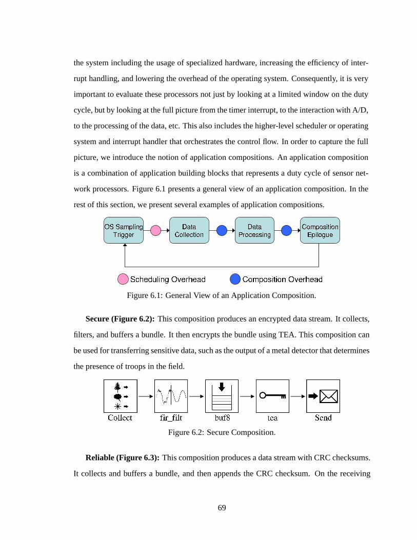
the system including the usage of specialized hardware, increasing the efficiency of inter-
rupt handling, and lowering the overhead of the operating system. Consequently, it is very
important to evaluate these processors not just by looking at a limited window on the duty
cycle, but by looking at the full picture from the timer interrupt, to the interaction with A/D,
to the processing of the data, etc. This also includes the higher-level scheduler or operating
system and interrupt handler that orchestrates the control flow. In order to capture the full
picture, we introduce the notion of application compositions. An application composition
is a combination of application building blocks that represents a duty cycle of sensor net-
work processors. Figure 6.1 presents a general view of an application composition. In the
rest of this section, we present several examples of application compositions.
Figure 6.1: General View of an Application Composition.
Secure (Figure 6.2):This composition produces an encrypted data stream. It collects,
filters, and buffers a bundle. It then encrypts the bundle using TEA. This composition can
be used for transferring sensitive data, such as the output of a metal detector that determines
the presence of troops in the field.
Figure 6.2: Secure Composition.
Reliable (Figure 6.3):This composition produces a data stream with CRC checksums.
It collects and buffers a bundle, and then appends the CRC checksum. On the receiving
69

end, the checksum can be used to determine transmission errors and force a retransmit of
the bundle if needed. This produces a reliable data stream from a higher-level perspective.
This composition can be applied to any data stream where bundle-level accuracy is a high
priority, including medical applications like bloodstream monitoring.
Figure 6.3: Reliable Composition.
Stats (Figure 6.4):This composition collects simple statistics for an input data stream.
It performs running average, minimum, maximum, and maintains the top 100 values. It can
be used for a simple characterization of a data stream from temperature or similar sensors.
Figure 6.4: Stats Composition.
Catalog (Figure 6.5): This composition catalogs a filtered data stream. It collects,
filters, and then tallies a bundle into a 4-bin histogram. This is well-suited to characterize
the occurrence content of a data stream, as in the case of engine temperature or wind speed.
Figure 6.5: Catalog Composition.
70

Detect (Figure 6.6):This composition detects an event by forming a threshold detec-
tion consensus with other chips whose threshold detection outputs come from off-chip.
This composition is useful for confidently detecting significant events such as seismic
anomalies.
Figure 6.6: Detect Composition.
Query (Figure 6.7): This composition searches a buffer for an input datum and trans-
mits the results. It can be used to confirm the occurrence of an event on the chip (searching
the buffer for an event number) or a pattern match (searching the buffer for a spectrogram
pattern).
Figure 6.7: Query Composition.
RLE stream (Figure 6.8):This composition compresses the output of a threshold de-
tector using Run Length Encoding (RLE). It collects a bundle, passes it through a threshold
detector, and then compresses it. RLE compression is well-suited for this composition’s
front-end because many threshold output streams have large runs of either 1 or 0.
71

Figure 6.8: RLEstream Composition.
Diff stream (Figure 6.9):This composition compresses a data stream using difference
compression and then buffers the data for transmission. This composition is well-suited for
efficient transfer of a data stream with very little fluctuation, such as air or body tempera-
ture.
Figure 6.9: Diff stream Composition.
AODV route (Figure 6.10): This composition implements the AODV routing algo-
rithm for inter-chip communication. It receives an AODV packet and either forwards the
packet as an RREQ message or replies to the sending chip with an RREP message. This is
useful for establishing routes for workloads that require interacting with other chips.
Figure 6.10: AODVroute Composition.
Simple route (Figure 6.11): This composition implements the levhop application and
propagates bundles to sink nodes. This is well-suited for the data gathering phase, where all
sensor processors transmit their data to a sink node for further and more complex analysis.
72

Figure 6.11: Simpleroute Composition.
6.3 Metrics
EPB (Energy Per Bundle): EPB represents the energy consumed by the processor
core to handle a bundle of samples from collecting and processing to sending and storing.
A bundle is the smallest unit of data processed in a chain of an application composition and
can contain a single or several samples depending on composition and sample precision.
For example, in Secure composition, if sample precision is eight bits, a bundle contains
eight samples. In this case, the EPB represents the energy consumed by the processor
in collecting eight samples, packaging them into two 32-bit pieces of data, encrypting
them using TEA, and finally transmitting them off-chip via radio or another communication
medium.
Figure 6.12: EPB Representation - EPB represents the total energy consumed by the entirecomposition to handle a bundle of samples.
xRT (times Real-Time): One important observation regarding sensor processors is
that, unlike conventional processors, higher performance is not necessarily advantageous.
It is mainly attributed to the fact that they perform most of their operations in real-time for
applications with slow changes, in which there is no benefit to running faster. Therefore, the
73

performance characteristics of a sensor processor transform into a binary function which
decides whether it is able or unable to service the composition in real-time. This depends on
the sample rate of the phenomenon. The normalized xRT can be employed as an effective
tool to evaluate the performance level of a sensor processor. It indicates how many times
faster the processor can perform the composition with respect to a 1Hz sample rate. The
xRT value determines the highest sample rate the processor can handle when performing
the specific composition. If a processor has an xRT value of 100 for Secure composition,
it can process up to 100Hz sample rate when performing Secure composition, i.e. it will
be able to handle blood pressure but not engine temperature. As long as the sample rate is
below that margin, it is not beneficial to increase the performance of the processor.
Figure 6.13: xRT Representation - xRT metric categorizes the phenomena into feasible andinfeasible ones.
CFP (Composition Footprint): CFP represents the storage requirement of the proces-
sor, which has a direct effect on the size and energy needs of the system. The relative
energy consumption of a sensor processor system is illustrated in Figure 6.14. The graph
shows the core and memory energy consumption for varied memory sizes in a subthresh-
old energy-efficient sensor processor, where the memory architectures are composed of 1/2
RAM and 1/2 ROM. It is clear that an increase in memory demands significantly increases
the overall energy consumption of the system. Hence, having small CFP is a critical factor
in the design of a sensor processor. As the definition of the composition contains all the
software overhead that links different components of the composition, it accounts for the
74

footprint of the operating system, if an operating system is employed.
Figure 6.14: Relative Energy Consumption of the Core and Memory
The metrics EPB and CFP together represent the overall energy consumption of the
system. It is important to have two separate metrics for these as most researchers report on
core energy consumption only. Moreover, if the results are reported on the actual fabricated
design, it is helpful to report on the energy consumption of the core separately provided the
core design has been the focus of the work or the size of the memory is larger than the CFP
for test purposes.
Case Study: In previous chapters we presented the first and second generations of
Subliminal processors. These processors are designed to minimize energy at the minimum-
energy voltage, which falls in the subthreshold region. In the first generation, we focused
on achieving a high code density using a CISC architecture and an accumulator-based de-
sign. We designed several variations of the processor to explore the design space in the
subthreshold voltage region and its characteristics. Based on our findings, we designed the
second generation of Subliminal processors using a RISC, LOAD-STOR architecture with
special modifications to increase code density. These two generations have a different in-
struction set architecture. Consequently it is not trivial to compare them, and by employing
the metrics proposed in this section comparison is straightforward.
Figure 6.15 presents the Composition Footprint (CFP) for several application compo-
75

sitions for the first and second generations of Subliminal processors. It is clear from this
chart that the second-generation processor has a significantly lower memory requirement
as discussed in Chapter 4.
Figure 6.15: Composition Footprint Comparison - CFP comparison is made between first-and second-generation Subliminal processors.
Figure 6.16 represents the EPB and xRT characteristics of several Subliminal proces-
sors from the first and second generations, for the RLEstream composition. Given a phe-
nomenon sample rate and a selected application composition, any processor that has xRT
equal or higher than the sample rate of that phenomenon is capable of meeting its real-time
demands when being processed by that application composition. For example, in Figure 14,
the Base model of the second-generation processor can perform RLEstream composition
for any sample rate equal to or smaller than 4.15 kHz. As for the EPB, the graph shows that
the first generation processors have to consume more than 4pJ to service a bundle (in this
case, a single sample) using the RLEstream composition. However, the second-generation
processor consumes less than half the energy to perform the same service. It is clear that al-
though these generations have different instruction set architectures, EPB and xRT metrics
76

provide a simple way to compare them.
Figure 6.16: Pareto Analysis of Several Subliminal Processors - Analysis is performed withrespect to RLEstream composition.
6.4 Summary and Insights
In this chapter, we proposed a novel approach to benchmarking for sensor processors.
Our approach is based on the following observations:
• Sensor processing has a distinctly different workload than that of traditional desk-
top and workstation class workloads, therefore, benchmark suites should exist that
address these differences.
• Sensor processing is a real-time processing activity, hence benchmarks developed
for this application space should account for how well a particular platform meets
the real-time demands of the application data source.
77

• In addition to performance metrics, the area, cost, and energy-constraints of sensor
platforms make it imperative to evaluate designs based on energy-consumed-per-task
and application memory demands.
Our presented novel sensor benchmark workload suite accounts for each of the above
observations. We introduce real-time, stream-oriented benchmark applications based on
the common activities of low- to medium-bandwidth sensor processors. Given these basic
application tasks, we demonstrate how stream compositions are formed to perform a non-
trivial representative task. These tasks are then fed data sources, based on a variety of
physical, environmental, mechanical, and biological data sources, to produce a real-time
stream processing experiment.
To evaluate these benchmarks and compare their performance across disparate plat-
forms, we propose the use of three new evaluation metrics: EPB (Energy Per Bundle), xRT
(times Real-Time), and CFP (Composition Footprint). EPB quantifies the amount of en-
ergy required (on average) to process a data element for a given application task and data
source. xRT measures the real-time performance of an application on a sensor platform,
indicating how many times faster than real-time the platform is able to handle the real-
time data source. Finally, CFP evaluates the memory demands of an application, which are
strong determinants of the cost and energy demands of a sensor processor. In each case, the
metrics are directly comparable across sensor processors. Hence, if designers implement
these application tasks and make the described measurements, it will become possible to
directly compare these diverse sensor platform designs.
Finally, we see a number of ways to enhance our benchmark suite.
• Incorporating sporadic and periodic events in a single composition. For example,
developing a composition that includes periodic data processing as well as sporadic
packet routing.
78

• Forming different data sets for each composition that result in average- or worst- case
EPB and xRT characteristics.
• Collaborating with sensor network system-level designers to introduce new compo-
sitions and improve the existing ones.
79

CHAPTER 7
Conclusions and Future Directions
7.1 Summary of Contributions
In this work, we explored the landscape of architectural energy optimization for low-
to mid-bandwidth sensor processing demands. We found that superthreshold (Vdd > Vth)
circuit implementations are too fast and energy-hungry for even the most simple of mi-
croarchitectures, leading us to the exploration of subthreshold (Vdd < Vth) circuit imple-
mentations. Additionally, we found the landscape of energy optimization for subthreshold
designs to be much more treacherous than that of superthreshold design. Specifically, we
found that:
• Area must be minimizedas it is a critical energy factor due to the dominance of
leakage energy at subthreshold voltages.
• Transistor utility must be maximizedbecause effective transistor computation off-
sets static leakage power, which permits a lower operating voltage and lower overall
energy consumption for the design.
• CPI must be minimizedat the same time, otherwise, gains through small area and
high transistor utility are squandered on inefficient computation.
80

We examined 21 different microarchitectural designs with varied datapath widths, de-
gree of pipelining, prefetching capability, and with varied register and memory architec-
tures. To achieve the fidelity necessary to evaluate their energy efficiency and performance
at subthreshold voltages, we produced a layout of each design in IBM 0.13µm fabrica-
tion technology. We confirmed our observed tenets of subthreshold design: simple but
CPI-efficient designs with high transistor utility and conservative area yield the most en-
ergy efficiency. We also found that many of our area- and performance-optimal designs
at subthreshold voltage levels are not the best performing designs at superthreshold volt-
ages, confirming our observation that the trade-offs surrounding energy-efficient design are
dramatically different in the subthreshold voltage domain.
Employing the lessons learned from our design space exploration, we built an ultra low-
energy RISC architecture. To address area concerns, we designed an extremely compact
12-bit instruction set, with a variety of optimizations to reduce code size. We found that
our best ISA design significantly improves code density, while only slightly aggravating
the size of the processor decoder logic. We introduced a memory system architecture with
row-address pre-decode, including ISA extensions that allow the programmer to specify
the most likely storage addresses for future accesses. This application-driven optimization,
not only improves the code density by reducing the number of bits to indicate the memory
address in the instruction, but also improves the performance by reducing the number of
cycles to access memory.
We completed a prototype physical design of one of the most energy-efficient first-
generation sensor processors. We briefly described the design, and the accompanying in-
frastructure on the test chip, which includes bulk-silicon solar cells, experimental memory
designs, and test harnesses. Our prototype chip has been manufactured by IBM in 0.13µm
technology and has been successfully tested, confirming the ideas presented in this work.
81

Finally, in an effort to more accurately evaluate sensor processors with different instruc-
tion sets and microarchitecture designs, we proposed a novel sensor benchmark workload
suite. The presented real-time, stream-oriented benchmark applications are based on the
common activities of low- to medium-bandwidth sensor processing workloads. Further-
more, we proposed the use of three new evaluation metrics: EPB (Energy Per Bundle),
xRT (times Real-Time), and CFP (Composition Footprint), which are more suited to eval-
uate sensor processors compared to more traditional metrics such as energy per instruction
and instructions per cycle. While EPB quantifies the energy consumption of the processor
by gauging the amount of energy required to process a data element for a given application
task and data source, xRT measures its real-time performance capability by indicating how
many times faster than real-time the platform is able to handle the real-time data source.
Additional CFP metric evaluates the memory demands of an application, which are strong
determinants of the cost and energy demands of a sensor processor. These three metrics are
directly comparable across sensor processors enabling direct comparison among current
diverse sensor platform designs.
7.2 Future Directions
82

APPENDICES
83

APPENDIX A
First-Generation Subliminal ISA Documentation
A.1 Architecture Overview
The first-generation Subliminal Processor -described in Chapter 3- is a CISC processor
with an accumulator-based ISA. Arithmetic and logic instructions therefore combine the
accumulator operand with an immediate value or with a second operand located in the uni-
fied instruction/data memory. The unified memory space is nibble addressable and contains
512 4-bit words. Instructions or data can be stored at any nibble. Located in the unified
memory, at the topmost memory locations, is the general purpose register file.
A.2 Variable Data Width Architecture
One special feature of the first-generation Subliminal Processor is that it has a variable
data width architecture. A specialized instruction is used to set the processors data width
to either two, four, or eight nibbles at any arbitrary place in the program. Operands can
therefore be up to eight nibbles in length.
While the first-generation Subliminal Processors ISA supports instructions referenc-
ing 2, 4 and 8-nibble operands, the processors ALU is only two nibbles wide. When the
84

operands are greater than two nibbles, the processor therefore performs arithmetic, logic,
and shift operations in an iterative fashion, working on only two nibbles at a time. For
example, a 32-bit addition is performed in four 8-bit addition cycles. After each addition
cycle, a carry out value is supplied to the next cycle as a carry in value.
To keep data of varying lengths organized in memory, data is either 2-nibble, 4-nibble,
or 8-nibble- aligned, depending on data width. Table A.1 shows how the programmer
should form a memory index when reading and writing aligned data. The programmer
references a memory location with the memory index only, never with the actual memory
address. Throughout this document, memory address refers to the entire 9-bit memory
address of the unified memory. Memory index, on the other hand, refers to the portion of
the memory address used by the programmer. Note that the size of a memory index varies
with data width.
Table A.1: Data Alignment in Memory
A.3 Memory Structure
As mentioned above, there is one memory space for both instructions and data. This
unified space is 512 nibbles. While the entire unified memory space is nibble addressable,
instructions and data are accessed in different size allotments. Instructions are read one
nibble at a time. Data, on the other hand, is read/written two nibbles at a time. For exam-
85

ple, a 4-nibble data operand is retrieved from memory in two 2-nibble reads. A 3-nibble
instruction is retrieved in from memory in three 1-nibble reads.
The register file, containing registers R0-R3, is located at the top of the unified memory
space. Each register is eight nibbles in length. R0, for example, begins at memory address
000000000 and ends at address 000000111, occupying eight lines in the memory. However,
depending on the data width, not all of these eight nibbles are utilized as the register. For
example, if the data width is four nibbles, only the first four memory lines of R0 will be
read or written to when referencing R0. The remaining four lines are free to be used as a
regular memory space to store instructions or data. In general, it is noteworthy that the top
32 lines of the memory is not necessarily dedicated to the register file and can always be
used as a regular memory space. Therefore, it is the programmers job to make sure he does
not overwrite register values when writing to the top 32 lines of memory.
Directly below the general purpose registers is the reset address (000100000). Upon
reset, the PC will be set to this particular address. At this address, the programmer can place
code that jumps to any location in the instruction/ data memory space. The programmer
has the freedom to place programs and/or data anywhere in this space.
A.4 Other Storage
In addition to the unified instruction/data memory, there is also an accumulator and
an address register bank. The accumulator space has four 8-bit memory locations. Like
the general purpose registers, the utilized portion of the accumulator depends on the data
width. If the data width is 4- nibbles, only the first two bytes of the accumulator contain
valid accumulator data.
The address register bank contains four 9-bit registers, S0-S3. For call and return func-
tionality, these registers are designed to hold the unified memorys 9-bit actual memory
address. S0-S3 can also store unified memory indexes for the indirect addressing mode
86

(see Addressing Modes below).
A.5 Addressing Modes
There are four basic addressing modes summarized in Table A.2. Addressing modes are
used in arithmetic, logical and load/store instructions. For the direct memory addressing
mode, the BLCK register is used to specify any remaining bits of a memory index (see
Data Width and Block Instruction). In the immediate addressing mode, only 2 bits are used
to specify an immediate value between 0 and 3. However, depending on the data width
this value is padded with extra 0 bits. Therefore, if the data width is 4 nibbles, in an ADD
instruction by an immediate value of 1, first the 2-bit immediate is extended to 16 bits with
extra 0s and then the addition is performed.
Table A.2: Addressing Mode Summary
87

A.6 Instruction Categories
A.6.1 Arithmetic and Logical Instructions
Arithmetic and logical instructions perform their specific operation on the accumula-
tor operand and a specified operand. The result is stored back to the accumulator. The
specified operand is chosen using the addressing mode. Instructions with register, indi-
rect memory, or immediate addressing modes are two nibbles. Instructions with the direct
memory addressing mode are three nibbles.
A.6.2 Shift Instruction
The shift instruction shifts the contents of the accumulator. As shown in the two fig-
ures above, this instruction has two forms, depending on the addressing mode: register or
immediate. When shifting by an amount stored in a register, this instruction is two nibbles.
When shifting by an immediate, this instruction is either two or three nibbles, depending
88

on the short/long bit. More details are provided in Table A.3, Table A.4, and Table A.5.
Table A.3: Shift Directions
Table A.4: Addressing Mode Summary for Shift Instructions
Table A.5: Short Immediate Data
A.6.3 Load/Store Instructions
89

The load/store instructions use the same addressing modes as the arithmetic and logic
instructions. The load instruction loads the data from the operand to the accumulator. The
store instruction stores the accumulator data at the operand’s location.
A.6.4 Data Width and Block Instruction
The DW BK instruction sets two of the internal registers of the processor, DW and
BLCK. DW indicates how many nibbles (two, four, or eight) should be manipulated during
all arithmetic, logic, shift and load/store operations. The data width operand is encoded, as
shown in Table A.6. Upon reset, DW is set to 00, representing 2 nibbles. When decreasing
the data width, it is advised to first reset the upper bits of the accumulator to 0. Otherwise,
undetermined behavior might arise in a shift to right instruction.
Table A.6: Operand Encoding
The BLCK register, on the other hand, represents the high-order memory index bits.
When using the direct memory addressing mode, only six of the possible eight memory
index bits are specified in an instruction. The value stored in the BLCK register resolves
the remaining unspecified highorder index bits. Table A.7 below illustrates how the BLCK
90

register fills in any unspecified bits in the direct memory addressing mode. Note again that
memory accesses are either 2-nibble, 4-nibble, or 8-nibble-aligned. The data width and
address block instruction is two nibbles.
Table A.7: Memory Index Bits
A.6.5 Address Register Instruction
The address register instruction is specially designed to manipulate the address reg-
isters. Following the opcode there are two mode bits that decide what operation needs
to be performed regarding an address register. Another two bits specifying the index of
the address register being processed follow the mode bits. Table A.8 provides the code,
mnemonic and description of each of the four modes of this instruction.
91

Table A.8: Different Modes of Operation for Address Instruction
A.6.6 Routine Instructions
The routine instruction provides the capability to call a routine and return from it. As
shown in the figure above and represented in Table A.9, the first bit after the opcode de-
termines whether the instruction is a call or a return. The call extension is followed by
two bits that represent the index of an address register which is used to store the next PC.
Following the two index bits, there are nine bits to represent the call destination. The return
extension is also followed by two bits to indicate an address register index. For the return,
the address stored in the given address register is the destination memory address. An un-
used bit follows these two index bits in the return extension. In order to properly call a
routine and return from it, the same address register should be used for both call and return.
Moreover, the programmer should make sure that the address register used for saving the
return address is not overwritten during the routine.
92

Table A.9: Routine Mode Summary
A.6.7 Jump instruction
The jump instruction jumps to the specified destination if the condition holds. Table
A.10 presents the condition description for the jump instruction. Note that one of the
conditions is no condition, which provides a non-conditional jump. Right after the 3-bit
code indicating the condition, 9 bits representing the destination follows.
Table A.10: Jump Condition Summary
93

A.6.8 NOP Instruction
This instruction does not affect the state of the processor.
94

APPENDIX B
Second-Generation Subliminal ISA Encoding
Table B.1: Second-Generation ISA Encoding
Verilog 11 10 9 8 7 6 5 4 3 2 1 0
ADD 0 0 0 K/G OPB OPB OPB OPB OPB OPA OPA OPA
SUB 0 0 1 K/G OPB OPB OPB OPB OPB OPA OPA OPA
AND 0 1 0 K/G OPB OPB OPB OPB OPB OPA OPA OPA
OR 0 1 1 K/G OPB OPB OPB OPB OPB OPA OPA OPA
XOR 1 0 0 K/G OPB OPB OPB OPB OPB OPA OPA OPA
LOAD 1 0 1 0 OPB OPB OPB OPB OPB OPA OPA OPA
SHFT 1 0 1 1 1 0 1 0 L/R OPA OPA OPA
PTR 1 1 1 0 MODE PSRC PSRC PSRC PSRC MODE PTR PTR
STOR 1 0 1 1 DEST DEST DEST DEST DEST SRC SRC SRC
PAGE 1 1 1 1 D/I NUM NUM NUM NUM NUM NUM NUM
JUMP 1 1 0 CND CND CND JDEST JDEST JDEST JDEST JDEST JDEST
NOP 1 0 1 1 1 0 1 1 0 0 0 0
RET 1 0 1 1 1 0 1 1 0 0 0 1
95

Table B.2: Second-Generation ISA Mnemonic Description
K/G G 0
K 1
OPA R 3 bit register address
OPB [# 0
R 1 0
[P 1 1 0
# 1 1 1
L/R LFT O Left
RGT 1 Right
MODE INC 0 0 PTR++
DEC 0 1 PTR--
SUB 1 0
LOAD 1 1
PTR P 2 bit destination pointer address
PSRC [# 0
[P 1 0
P 1 1
DEST [# 0
[P 1 0 0
SRC
D/I D 0 DMEM page number
I 1 IMEM page number
NUM 7 bit page number
CND NOC 0 0 0 No condition
C 0 0 1 Carry
NC 0 1 0 Not Carry
Z 0 1 1 Zero
NZ 1 0 0 Not Zero
CZ 1 0 1 Carry or Zero
NCZ 1 1 0 Neither Carry nor Zero
CALL 1 1 1 Call
JDEST lowest 6 bit of destination address
***********************************************************************************************
3 bit register address
***********************************************************************************************
***********************************************************************************************
***********************************************************************************************
***********************************************************************************************
lowest 4 bit direct memory address
2 bit pointer address
***********************************************************************************************
lowest 3 bit direct memory address
2 bit pointer address (content of the pointer)
2 bit pointer address (the pointer itself)
PTR -= PSRC
PTR = PSRC
***********************************************************************************************
2 bit immidiate value
***********************************************************************************************
***********************************************************************************************
lowest 4 bit direct memory address
3 bit register address
2 bit pointer address
R0 = opa + opb
opa = opa + opb
***********************************************************************************************
96

APPENDIX C
Selective Developed Applications in First-GenerationSubliminal Assembly Language
C.1 Buffer8
Implements a saturating buffer of 8-bit chunks using a buffer pointer. A full signal is
asserted when the buffer becomes full. Any further insertion into a full buffer overwrites
the last entry.
//Constants.const INPUT 16.const CUR_SIZE 17.const MAX_SIZE 18.const FULL 19.const BUF_PTR 20
//Sections.section 128 8
( 55, 2, 8, 0, 15 ).section 168 8
( 11, 22, 0, 0, 0, 0, 0, 0 )
//Begin CodeDW_BK 8 0
LOAD [# INPUT ]STOR R 1
//Store datum to bufferLOAD [# BUF_PTR ]ADD [# CUR_SIZE ]ADDR STOR S 0LOAD R 1STOR [S 0 ]
//Limit checkLOAD [# CUR_SIZE ]STOR R 1
97

SUB [# MAX_SIZE ]JUMP NCZ # <not_full>LOAD # 1STOR [# FULL ]JUMP NOC # <end>
not_full: LOAD R 1ADD # 1STOR [# CUR_SIZE ]
end: NOP
C.2 RLE Compression
Implements RLE compression using 32-bit chunks. An input array is compressed using
Run Length Encoding (RLE), where an input stream of ”x x x y y y” is compressed to ”3 x
3 y”, for example. An output array is formed in contiguous memory immediately following
the input array.
//Constants.const IN_BASE 16.const OUT_BASE 17
//Sections.section 128 8
( 12, 16, ).section 144 8 //Input stream
( afffffff, bfffffff, cfffffff, deadbeef, ).section 176 8 //Output stream
( 0, 0, 0, 0, 0, 0, )
//Begin CodeDW_BK 8 0
LOAD [# IN_BASE ]ADDR STOR S 0LOAD [# OUT_BASE ]ADDR STOR S 1LOAD # 1STOR R 0LOAD [S 0 ]STOR R 1
while: LOAD # 0ADDR INC S 0ADDR LOAD S 0SUB [# OUT_BASE ]JUMP Z # <end>
if: LOAD [S 0 ]SUB R 1JUMP NZ # <else>LOAD R 0ADD # 1
98
STOR R 0JUMP NOC # <while>NOP
else: LOAD R 0STOR [S 1 ]ADDR INC S 1LOAD R 1STOR [S 1 ]ADDR INC S 1LOAD # 1STOR R 0LOAD [S 0 ]STOR R 1JUMP NOC # <while>
end: NOP
C.3 Consensus
A binary, majority consensus is performed using four binary inputs. If a majority of the
inputs are 1, then a 1 is output. Otherwise, a 0 is output.
//Constants.const VOTE1 16.const VOTE2 17.const VOTE3 18.const VOTE4 19.const MAJ 20
//Sections.section 128 8
( 0, 1, 1, 1, 0 )
//Begin CodeDW_BK 8 0
LOAD [# VOTE1 ]ADD [# VOTE2 ]ADD [# VOTE3 ]ADD [# VOTE4 ]SHFT RGT # SHRT 1SUB # 1JUMP C # <no_maj>LOAD # 1JUMP NOC # <end>
no_maj: LOAD # 0end: STOR [# MAJ ]
99
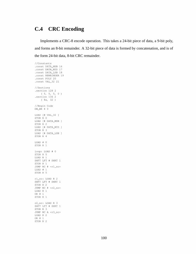
C.4 CRC Encoding
Implements a CRC-8 encode operation. This takes a 24-bit piece of data, a 9-bit poly,
and forms an 8-bit remainder. A 32-bit piece of data is formed by concatenation, and is of
the form 24-bit data, 8-bit CRC remainder.
//Constants.const DATA_MSB 16.const DATA_MID 17.const DATA_LSB 18.const REMAINDER 19.const POLY 20.const VAL_32 21
//Sections.section 128 2
( 5, 5, 5, 0 ).section 136 2
( 8a, 32 )
//Begin CodeDW_BK 8 0
LOAD [# VAL_32 ]STOR R 0LOAD [# DATA_MSB ]STOR R 2LOAD [# DATA_MID ]STOR R 3LOAD [# DATA_LSB ]STOR R 4
LOAD # 0STOR R 1
loop: LOAD # 0STOR R 5LOAD R 1SHFT LFT # SHRT 1STOR R 1JUMP NC # <r1_nc>LOAD # 1STOR R 5
r1_nc: LOAD R 2SHFT LFT # SHRT 1STOR R 2JUMP NC # <r2_nc>LOAD R 1OR # 1STOR R 1
r2_nc: LOAD R 3SHFT LFT # SHRT 1STOR R 3JUMP NC A <r3_nc>LOAD R 2OR # 1STOR R 2
100

r3_nc: LOAD R 4SHFT LFT # SHRT 1STOR R 4JUMP NC A <r4_nc>LOAD R 3OR # 1STOR R 3
r4_nc: LOAD R 5SUB # 1STOR R 5JUMP NZ # <no_xor>LOAD R 1XOR [# POLY ]STOR R 1
no_xor: LOAD R 0SUB # 1STOR R 0JUMP NZ # <loop>
LOAD R 1STOR [# REMAINDER ]
C.5 4-Bin Histogram
Implements a 4-bin, variable threshold histogram. A 32-bit piece of data is categorized
and a corresponding bin count is incremented.
//Constants.const THD_PTR 16.const BIN_PTR 17.const INPUT 25
//Sections.section 128
( 12, 15 ).section 144
( 5, 10, 15 ).section 168
( 0, 0, 0, 0 ).section 200
( 16 )
//Begin CodeDW_BK 8 0
LOAD [# THD_PTR ]ADDR STOR S 0LOAD [# BIN_PTR ]ADDR STOR S 1LOAD [# INPUT ]STOR R 1LOAD # 1STOR R 2
101

loop: LOAD R 1SUB [S 0 ]JUMP C # <tally>
ADDR INC S 0ADDR INC S 1LOAD [# BIN_PTR ]ADDR SUB S 0JUMP NZ # <loop>
tally: LOAD R 2ADD [S 1 ]STOR [S 1 ]
C.6 FIR Filter
Implements a signed, 2-tap, 4-input, 32-bit FIR integer filter. An input array and a filter
array are convolved to form an output array. To save memory, the input array is overwritten
by the output array.
//Constants.const X_BASE_START 39.const X_BASE_END 40.const FILT_BASE_START 41.const FILT_BASE_END 42
//Sections.section 256 8 //FILTER Data
( 1, 1, ).section 272 8 //Input Data
( 1, 1, 2, 2, 0, ).section 312 8 //Bounds
( 25, 21, 20, 22, )
//Begin CodeDW_BK 8 0
LOAD [# X_BASE_START ]ADDR STOR S 0NOP
start_outer: LOAD [S 0 ]STOR R 3LOAD # 0STOR [S 0 ]LOAD [# FILT_BASE_START ]ADDR STOR S 1ADDR LOAD S 0ADDR STOR S 2NOP
start_inner: LOAD [S 1 ]STOR R 1LOAD R 3STOR R 0JUMP NOC # <mult_start>
102

filt_ret: LOAD R 2ADD [S 2 ]STOR [S 2 ]ADDR INC S 1ADDR INC S 2ADDR LOAD S 1SUB [# FILT_BASE_END ]JUMP NZ # <start_inner>ADDR DEC S 0ADDR LOAD S 0SUB [# X_BASE_END ]JUMP NZ # <start_outer>JUMP NOC # <end>
// Integer multiplication startmult_start: LOAD # 0STOR R 2
mult_loop: LOAD R 0ADD # 0JUMP Z # <filt_ret>SHFT RGT # SHRT 1STOR R 0JUMP NC # <mult_inc>
LOAD R 2ADD R 1STOR R 2
mult_inc: LOAD R 1SHFT LFT # SHRT 1STOR R 1JUMP NOC # <mult_loop>//Integer multiplication end
end: NOP
C.7 Routing
Implements a simple, level-based routing scheme. Each node has an id and a level. All
messages are propogated to higher levels only, otherwise incoming messages are dropped.
//Constants.const NODE_INFO 16.const NODE_DATA 17.const AND_LVL_MASK 18.const AND_ID_MASK 19.const I_BUF_INFO 20.const I_BUF_DATA 21.const O_BUF_INFO 22.const O_BUF_DATA 23
//Sections.section 128 8
( ffff5555, 0, 0000ffff, ffff0000, ).section 160 8
( 5555aaaa, 66666666, 0, 0, )
103

//Begin CodeDW_BK 8 0
//Get info to IBUFLOAD [# I_BUF_INFO ]STOR R 0
//Get packet levelAND [# AND_LVL_MASK ]STOR R 1
//Get receiver node levelLOAD [# NODE_INFO ]AND [# AND_LVL_MASK ]STOR R 2
//Compare levelsSUB R 1JUMP NC # <no_send>
//Send updated packet to O_BUFLOAD R 0AND [# AND_ID_MASK ]OR R 2STOR [# O_BUF_INFO ]LOAD [# I_BUF_DATA ]STOR [# O_BUF_DATA ]
no_send: NOP
C.8 Tiny Encryption Algorithm
Implements one cycle of the Tiny Encryption Algorithm (TEA). Two input variables,
X and Y, are updated using four constants A-D and DELTA, in the following manner:
X+ = [(Y << 4) + a]⊕ [Y + delta]⊕ [(Y >> 5) + b]
Y + = [(X << 4) + c]⊕ [X + delta]⊕ [(X >> 5) + d]
//Constants.const delta 32.const var_a 33.const var_b 34.const var_c 35.const var_d 36.const var_x 37.const var_y 38
//Sections.section 256 8
( 9e3779b9, fa9851f1, 9c4ba642, cad3793, ).section 288 8
104

( 397fc514, a527931c, 258a4f31, )
//Begin CodeDW_BK 8 0
LOAD # 0STOR R 1LOAD [# var_x ]STOR R 2LOAD [# var_y ]STOR R 3LOAD R 1ADD [# delta ]STOR R 1LOAD R 2SHFT LFT # LONG 4ADD [# var_a ]STOR R 0LOAD R 2ADD R 1XOR R 0STOR R 0LOAD R 2SHFT RGT # LONG 5ADD [# var_b ]XOR R 0ADD R 3STOR R 3SHFT LFT # LONG 4ADD [# var_c ]STOR R 0LOAD R 3ADD R 1XOR R 0STOR R 0LOAD R 3SHFT RGT # LONG 5ADD [# var_d ]XOR R 0ADD R 2STOR R 2
105

BIBLIOGRAPHY
106

[1] ARM Ltd. Website.http://www.arm.com.
[2] ATMEL Website.http://www.atmel.com.
[3] Intel mote research project website.http://www.intel.com/research/exploratory/motes.htm.
[4] Intel pxa255 xscale processor datasheet.http://www.intel.com/design/pca/prodbref/252780.htm.
[5] Online resource for information on the data compression field.http://www.data-compression.info/Algorithms/RLE/.
[6] University of california, los angeles, wireless integrated network sensors website.http://www.janet.ucla.edu/WINS/.
[7] Wireless sensing networks project at rockwell scientific website.http://wins.rsc.rockwell.com.
[8] Spec. spec benchmark suite release 1.0. 1989.
[9] Monitoring in anaesthesia.http://www.liv.ac.uk/̃afgt/PhysMeasNotes.pdf, 2004.
[10] Multilog, multilogpro and ecolog weather stations. www.fourier-sys.com/pdfs/dataloggers/, 2004.
[11] Thomas David Burd.Subthreshold leakage modeling and reduction techniques. PhDthesis, University of California, Berkeley, 2001.
[12] C.E.Perkins. Ad-hoc on-demand distance vector routing.MILCOM Panel on Ad HocNetworks, http://cireseer.ist.psu.edu/article/perkins97adhoc.html.
[13] Chee-Yee Chong. Sensor networks: Evolution, opportunities and challanges. InProceedings of the IEEE , Volume: 91 , Issue: 8, August 2003.
[14] Virantha Ekanayake, Clinton Kelly, and Rajit Manohar. An ultra low-power processorfor sensor networks. InProceedings of the 11th international conference on Architec-tural support for programming languages and operating systems, 2004.
[15] J. Feng, F. Koushanfar, and M. Potkonjak. System-architectures for sensor networksissues, alternatives, and directions. InProceedings of IEEE International Conferenceon Computer Design: VLSI in Computers and Processors, 2002.
[16] M. R. Guthaus, J. S. Ringenberg, D. Ernst, T. M. Austin, T. Mudge, , and R. B. Brown.Mibench: A free, commercially representative embedded benchmark suite. InIEEE4th Annual Workshop on Workload Characterization, 2001.
[17] Mark Hempstead, Nikhil Tripathi, Patrick Mauro, Gu-Yeon Wei, and David Brooks.An ultra low power system architecture for sensor network applications. InInterna-tional Symposium on Computer Architecture, 2005.
107

[18] Jason Lester Hil.System Architecture for Wireless Sensor Networ. PhD thesis, Uni-versity of California, Berkeley, 2003.
[19] James Kao, Siva Narendra, and Anantha Chandrakasan. Subthreshold leakage mod-eling and reduction techniques. InProceedings of the international conference onComputer-aided design, June 2002.
[20] F. Koushanfar, V. Prabhu, M. Potkonjak, J.M., and Rabaey. Processors for mobileapplications. InInternational Conference on Computer Design, 2000.
[21] Chunho Lee, Miodrag Potkonjak, and William H. Mangione-Smith. Mediabench:A tool for evaluating and synthesizing multimedia and communicatons systems. InMICRO 1997, 1997.
[22] J. D. Meindl and J. A. Davis. The fundamental limit on biary switching energy forterascale integration (TSI). InIEEE JSSCC vol. 35, February 2002.
[23] J. Rabaey, J. Ammer, T. Karalar, B. Otis S. Li, M. Sheets, and T. Tuan. Picoradios forwireless sensor networks: The next challenge in ultra-low-power design. InProceed-ings of the International Solid-State Circuits Conference, San Francisco, February2002.
[24] Curt Schurgers and Mani B. Srivastava. Energy efficient routing in wireless sensornetworks.MILCOM’01, Vienna, VA, October 2001.
[25] Brett A. Warneke and Kristofer S.J. Pister. An ultra-low energy microcontroller forsmart dust wireless sensor networks. InInternational Solid-State Circuits Conference,2004.
[26] Brett Alan Warneke. Ultra-Low Energy Architecture and Circuits for Cubic Mil-limeter Distributed Wireless Sensor Networks. PhD thesis, University of California,Berkeley, 2003.
[27] D. J. Wheeler and R. M. Needham. TEA, a tiny encryption algorithm.Lecture Notesin Computer Science, 1008, 1995.
[28] Ross A. Williams. A painless guide to crc error detection algorithms.http://www.repairfaq.org/filipg/LINK/Fcrc v3.html.
[29] Bo Zhai, David Blaaw adn Dennis Sylvester, and Krisztian Flautner. Theoretical andpractical limits of dynamic voltage scaling. InProceedings of DAC, 2004.
108