architecture and hardware design of lossless...
TRANSCRIPT
Architecture and Hardware Design of Lossless
Compression Algorithms for Direct-Write Maskless
Lithography Systems
Hsin-I Liu
Electrical Engineering and Computer SciencesUniversity of California at Berkeley
Technical Report No. UCB/EECS-2010-47
http://www.eecs.berkeley.edu/Pubs/TechRpts/2010/EECS-2010-47.html
April 29, 2010

Copyright © 2010, by the author(s).All rights reserved.
Permission to make digital or hard copies of all or part of this work forpersonal or classroom use is granted without fee provided that copies arenot made or distributed for profit or commercial advantage and that copiesbear this notice and the full citation on the first page. To copy otherwise, torepublish, to post on servers or to redistribute to lists, requires prior specificpermission.
Architecture and Hardware Design of Lossless Compression Algorithms forDirect-Write Maskless Lithography Systems
by
Hsin-I Liu
A dissertation submitted in partial satisfaction of the
requirements for the degree of
Doctor of Philosophy
in
Engineering - Electrical Engineering and Computer Sciences
in the
Graduate Division
of the
University of California, Berkeley
Committee in charge:Professor Avideh Zakhor, Chair
Professor Borivoje NikolicProfessor Peter Y Yu
Spring 2010
The dissertation of Hsin-I Liu, titled Architecture and Hardware Design of LosslessCompression Algorithms for Direct-Write Maskless Lithography Systems is approved:
Chair Date
Date
Date
University of California, Berkeley

Architecture and Hardware Design of Lossless Compression Algorithms for
Direct-Write Maskless Lithography Systems
Copyright c⃝ 2010
by
Hsin-I Liu
1
Abstract
Architecture and Hardware Design of Lossless Compression Algorithms for Direct-Write
Maskless Lithography Systems
by
Hsin-I Liu
Doctor of Philosophy in Engineering - Electrical Engineering and Computer Sciences
University of California, Berkeley
Professor Avideh Zakhor, Chair
Future lithography systems must produce chips with smaller feature sizes, while maintaining
throughput comparable to today’s optical lithography systems. This places stringent data
handling requirements on the design of any direct-write maskless system. To achieve the
throughput of one wafer layer per minute with a direct-write maskless lithography system,
using 22 nm pixels for 45 nm technology, a data rate of 12 Tb/s is required. A recently pro-
posed datapath architecture for direct-write lithography systems shows that lossless compres-
sion could play a key role in reducing the system throughput requirements. This architecture
integrates low complexity hardware-based decoders with the writers, in order to decode a
compressed rasterized layout in real time. To this end, a spectrum of lossless compression
algorithms have been developed for rasterized integrated circuit (IC) layout data to provide
2
a tradeoff between compression efficiency and hardware complexity. In this thesis, I extend
Block Context Copy Combinatorial Code (Block C4), a previously proposed lossless com-
pression algorithm, to Block Golomb Context Copy Code (Block GC3), in order to reduce
the hardware complexity, and to improve the system throughput. In particular, the hierar-
chical combinatorial code in Block C4 is replaced by Golomb run-length code to result in
Block GC3. Block GC3 achieves minimum compression efficiency of 6.5 for 1024 × 1024,
5-bit Poly layer layouts in 130 nm technology. Even though this compression efficiency is
15% lower than that of Block C4, Block GC3 decoder is 40% smaller in area than Block C4
decoder.
In this thesis, I also illustrate hardware implementation of Block GC3 decoder with FPGA
and ASIC synthesis flow. For one Block GC3 decoder with 8 × 8 block size, 3233 slice flip-
flops and 3086 4-input LUTs are utilized in a Xilinx Virtex II Pro 70 FPGA, corresponding
to 4% of its resources. The decoder has 1.7 KB internal memory, which is implemented
with 36 block memories, corresponding to 10% of the FPGA resources. The system runs
at 100 MHz clock rate, with the overall output rate of 495 Mb/s for a single decoder. The
corresponding ASIC implementation results in a 0.07 mm2 design with the maximum output
rate of 2.47 Gb/s.
I also explore the tradeoff between encoder complexity and compression efficiency, with
a case study for reflective E-beam lithography (REBL) system. In order to accommodate
REBL’s rotary writing system, I introduce Block RGC3, a variant of Block GC3, in order
to adapt to the diagonal repetition of the rotated layout images. By increasing the encoding
3
complexity, Block RGC3 achieves minimum compression efficiency of 5.9 for 256 × 2048,
5-bit Metal-1 layer layouts in 65 nm technology with 40 KB buffer; this outperforms Block
GC3 and all existing lossless compression algorithms, while maintaining a simple decoder
architecture.
i
To my family,
for their help and support along the way.
ii
Contents
List of Figures iv
List of Tables vii
1 Introduction 11.1 Introduction to Maskless Lithography . . . . . . . . . . . . . . . . . . . . . . 11.2 The Architecture of Maskless Lithography Systems . . . . . . . . . . . . . . 21.3 Datapath Implementation of Maskless Lithography Systems . . . . . . . . . 41.4 Related Work on Maskless Lithography . . . . . . . . . . . . . . . . . . . . . 61.5 Scope of the Dissertation . . . . . . . . . . . . . . . . . . . . . . . . . . . . . 10
2 Prior Work on Lossless Data Compression Algorithms for Maskless Lithog-raphy Systems 122.1 Overview of C4 . . . . . . . . . . . . . . . . . . . . . . . . . . . . . . . . . . 132.2 Block C4 . . . . . . . . . . . . . . . . . . . . . . . . . . . . . . . . . . . . . . 172.3 Compression Efficiency Results . . . . . . . . . . . . . . . . . . . . . . . . . 22
3 Block GC3 Lossless Compression Algorithm 253.1 Introduction . . . . . . . . . . . . . . . . . . . . . . . . . . . . . . . . . . . . 253.2 Block GC3 . . . . . . . . . . . . . . . . . . . . . . . . . . . . . . . . . . . . . 263.3 Selectable Bucket Size for Golomb Run-Length Decoder . . . . . . . . . . . . 303.4 Fixed Codeword for Huffman Decoder . . . . . . . . . . . . . . . . . . . . . 323.5 Summary . . . . . . . . . . . . . . . . . . . . . . . . . . . . . . . . . . . . . 33
4 Hardware Design of Block C4 and Block GC3 Decoders 364.1 Introduction . . . . . . . . . . . . . . . . . . . . . . . . . . . . . . . . . . . . 364.2 Block C4 . . . . . . . . . . . . . . . . . . . . . . . . . . . . . . . . . . . . . . 38
4.2.1 Linear Predictor . . . . . . . . . . . . . . . . . . . . . . . . . . . . . 384.2.2 Region Decoder . . . . . . . . . . . . . . . . . . . . . . . . . . . . . . 404.2.3 Huffman Decoder . . . . . . . . . . . . . . . . . . . . . . . . . . . . . 45
iii
4.2.4 HCC Decoder . . . . . . . . . . . . . . . . . . . . . . . . . . . . . . . 484.2.5 Address Generator . . . . . . . . . . . . . . . . . . . . . . . . . . . . 564.2.6 Control Unit . . . . . . . . . . . . . . . . . . . . . . . . . . . . . . . . 574.2.7 On-Chip Buffering . . . . . . . . . . . . . . . . . . . . . . . . . . . . 59
4.3 Block GC3 . . . . . . . . . . . . . . . . . . . . . . . . . . . . . . . . . . . . . 614.4 FPGA Emulation Results . . . . . . . . . . . . . . . . . . . . . . . . . . . . 624.5 ASIC Synthesis and Simulation Results . . . . . . . . . . . . . . . . . . . . . 654.6 Summary . . . . . . . . . . . . . . . . . . . . . . . . . . . . . . . . . . . . . 69
5 Integrating Decoder with Maskless Writing System 705.1 Introduction . . . . . . . . . . . . . . . . . . . . . . . . . . . . . . . . . . . . 705.2 Input/Output data buffering . . . . . . . . . . . . . . . . . . . . . . . . . . . 715.3 Control of Error Propagation . . . . . . . . . . . . . . . . . . . . . . . . . . 725.4 Data Packaging . . . . . . . . . . . . . . . . . . . . . . . . . . . . . . . . . . 745.5 Summary . . . . . . . . . . . . . . . . . . . . . . . . . . . . . . . . . . . . . 75
6 Block RGC3: Lossless Compression Algorithm for Rotary Writing Sys-tems 776.1 Introduction . . . . . . . . . . . . . . . . . . . . . . . . . . . . . . . . . . . . 776.2 Datapath for REBL System . . . . . . . . . . . . . . . . . . . . . . . . . . . 786.3 Adapting Block GC3 to REBL Data . . . . . . . . . . . . . . . . . . . . . . 81
6.3.1 Modifying the Copy Algorithm . . . . . . . . . . . . . . . . . . . . . 816.3.2 Decreasing the Block Size . . . . . . . . . . . . . . . . . . . . . . . . 826.3.3 Compression for Segmentation Information . . . . . . . . . . . . . . . 866.3.4 Impact on Encoding Complexity . . . . . . . . . . . . . . . . . . . . . 87
6.4 Summary . . . . . . . . . . . . . . . . . . . . . . . . . . . . . . . . . . . . . 89
7 Conclusions and Future Work 92
Bibliography 97
A Proof of NP-Completeness for Two-Dimensional Region Segmentation 104
B Schematics of Block GC3 Decoder 106
iv
List of Figures
1.1 Schematic diagram of maskless EUV lithography system [35] [29]. . . . . . . 31.2 Data delivery path of direct-write lithography systems. . . . . . . . . . . . . 51.3 Block diagram of pre-alpha MAPPER maskless lithography system [24]. . . . 81.4 Block diagram of PML2 system [34] [25]. . . . . . . . . . . . . . . . . . . . . 81.5 Block diagram of Vistec system showing the combination of single shaped
beam path (light green) and multi shaped beam path (dark green) [34] [36]. . 91.6 Block diagram of REBL system [33]. . . . . . . . . . . . . . . . . . . . . . . 9
2.1 (a)Repetitive and (b) non-repetitive layouts. . . . . . . . . . . . . . . . . . . 142.2 Block diagram of C4 encoder and decoder for gray-level images. . . . . . . . 152.3 Three-pixel linear prediction with saturation in C4. . . . . . . . . . . . . . . 172.4 Illustration of a copy region. . . . . . . . . . . . . . . . . . . . . . . . . . . . 182.5 Illustration of a few potential copy regions that may be defined on the same
layout. . . . . . . . . . . . . . . . . . . . . . . . . . . . . . . . . . . . . . . . 182.6 Segmentation map of (a) C4 vs. (b) Block C4. . . . . . . . . . . . . . . . . . 202.7 Three-block prediction for encoding segmentation in Block C4. . . . . . . . . 212.8 (a) Block C4 segmentation map (b) with context-based prediction. . . . . . . 212.9 The compression efficiency comparison among different lossless compression
algorithms [10]. . . . . . . . . . . . . . . . . . . . . . . . . . . . . . . . . . . 24
3.1 The encoder/decoder architecture of Block GC3. . . . . . . . . . . . . . . . . 273.2 Golomb run-length encoding process. . . . . . . . . . . . . . . . . . . . . . . 283.3 Visualization of pixel error location for a layout image. . . . . . . . . . . . . 283.4 Compression efficiency and buffer size tradeoff for Block C4 and Block GC3. 303.5 Block diagram of Golomb run-length decoder. . . . . . . . . . . . . . . . . . 313.6 Image error value and Huffman codewords comparison, for (a) poly layer and
(b) n-active layer. . . . . . . . . . . . . . . . . . . . . . . . . . . . . . . . . . 34
4.1 Functional block diagram of the decoder. . . . . . . . . . . . . . . . . . . . . 374.2 The block diagram of Merge/Control block. . . . . . . . . . . . . . . . . . . 38
v
4.3 The block diagram of Linear Predictor. . . . . . . . . . . . . . . . . . . . . . 394.4 The algorithm of 3-pixel based linear prediction. . . . . . . . . . . . . . . . . 394.5 The context prediction algorithm for the segmentation information. . . . . . 414.6 The block diagram of the region decoder. . . . . . . . . . . . . . . . . . . . . 414.7 The block diagram of the segmentation predictor. . . . . . . . . . . . . . . . 434.8 The illustration of converting segmentation information into the pixel domain. 444.9 The timing diagram of the read/write operation of the delay chain. . . . . . 444.10 The block diagram of the Golomb run-length decoder. . . . . . . . . . . . . . 454.11 The block diagram of the Huffman decoder. . . . . . . . . . . . . . . . . . . 464.12 The control flow of the Huffman decoder. . . . . . . . . . . . . . . . . . . . . 474.13 Two-level HCC with a block size H = 4 for each level. . . . . . . . . . . . . . 494.14 The decoding process of HCC in (a) top-to-bottom fashion and (b) parallel
scheme. The timing analysis of (c) top-to-bottom fashion and (d) parallelscheme. . . . . . . . . . . . . . . . . . . . . . . . . . . . . . . . . . . . . . . 51
4.15 The control flow for one level of the HCC decoder. . . . . . . . . . . . . . . . 524.16 The encoding/decoding algorithm for uniform coding. . . . . . . . . . . . . . 544.17 The schematic of the uniform decoder. . . . . . . . . . . . . . . . . . . . . . 544.18 The decoding flow of the combinatorial decoding. . . . . . . . . . . . . . . . 564.19 The schematic of the combinatorial decoder. . . . . . . . . . . . . . . . . . . 574.20 The block diagram of the address generator. . . . . . . . . . . . . . . . . . . 584.21 The detail block diagram of the control block. . . . . . . . . . . . . . . . . . 594.22 The detail block diagram of the synchronous FIFO. . . . . . . . . . . . . . . 614.23 The block diagram of the Golomb run-length decoder. . . . . . . . . . . . . . 624.24 (a)The BEE2 system [19]; (b) FPGA emulation architecture of Block GC3
decoder. . . . . . . . . . . . . . . . . . . . . . . . . . . . . . . . . . . . . . . 64
5.1 The block diagram of the history buffer with ECC. . . . . . . . . . . . . . . 745.2 Data distribution architecture of Block GC3 decoder . . . . . . . . . . . . . 75
6.1 (a)Block diagram of the REBL Nanowriter; (b) detailed view of the rotarystage [33]. . . . . . . . . . . . . . . . . . . . . . . . . . . . . . . . . . . . . . 79
6.2 The data-delivery path of the REBL system. . . . . . . . . . . . . . . . . . . 806.3 Two copy methods: (a) Block GC3: only horizontal/vertical copy is allowed;
(b) Block RGC3: blocks may be copied from anywhere within the searchrange. In both cases, the dashed areas must be stored in the history buffer. . 82
6.4 Layout image of the REBL system: (a) Original layout image; (b) fitting theimage to an H W block grid; (c) an example of image repetition, given anedge oriented at tan-1(2) with respect to the pixel grid. . . . . . . . . . . . . 84
6.5 Segmentation map of a 256× 1024, 25∘-oriented image. . . . . . . . . . . . . 85
B.1 The block diagram of BlockGC3 decoder. . . . . . . . . . . . . . . . . . . . . 107B.2 The block diagram of region decoder. . . . . . . . . . . . . . . . . . . . . . . 108B.3 The block diagram of the segmentation predictor. . . . . . . . . . . . . . . . 108
vi
B.4 The block diagram of Golomb run-length decoder for region decoder. . . . . 109B.5 The block diagram of the delay chain. . . . . . . . . . . . . . . . . . . . . . . 109B.6 The block diagram of linear predictor. . . . . . . . . . . . . . . . . . . . . . 110B.7 The block diagram of Huffman decoder. . . . . . . . . . . . . . . . . . . . . . 111B.8 The block diagram of Golomb run-length decoder for image error location. . 112B.9 The block diagram of the region decoder. . . . . . . . . . . . . . . . . . . . . 113B.10 The block diagram of the history buffer. . . . . . . . . . . . . . . . . . . . . 113B.11 The block diagram of FIFO. . . . . . . . . . . . . . . . . . . . . . . . . . . . 114B.12 The block diagram of the control block. . . . . . . . . . . . . . . . . . . . . . 114
vii
List of Tables
1.1 List of E-beam direct-write lithography projects [34]. . . . . . . . . . . . . . 7
2.1 Comparison of compression ratio and encode times of C4 vs. Block C4 [10]. . 23
3.1 Compression efficiency comparison between Block C4 and Block GC3 for dif-ferent layers of layouts. . . . . . . . . . . . . . . . . . . . . . . . . . . . . . . 29
3.2 Compression efficiency comparison between different Huffman code tables. . 33
4.1 Estimated hardware performance comparison of different data path of direct-write maskless lithography systems. . . . . . . . . . . . . . . . . . . . . . . . 63
4.2 Synthesis summary of Block GC3 decoder. . . . . . . . . . . . . . . . . . . . 644.3 ASIC synthesis result of Block GC3 decoder. . . . . . . . . . . . . . . . . . . 664.4 Power estimate of Block GC3 decoder with different switching activity factors
� . . . . . . . . . . . . . . . . . . . . . . . . . . . . . . . . . . . . . . . . . . 68
6.1 Properties of the test layout images. . . . . . . . . . . . . . . . . . . . . . . . 806.2 Average compression efficiency comparison of two copy methods. . . . . . . . 836.3 Bit allocation of Block GC3 compressed streams, using diagonal copying. . . 856.4 Compression efficiency comparison for entropy codings. . . . . . . . . . . . . 886.5 Encoding times comparison between Block RGC3 and Block GC3. . . . . . . 896.6 Compression efficiency comparison of different compression algorithms. . . . 906.7 Block RGC3 Compression efficiency comparison of different layout images. . 91

viii
Acknowledgments
I would like to acknowledge many contributors to this work. First and foremost, I would
like to express my sincerest gratitude to my research advisor, Prof. Avideh Zakhor, for all
things great or small. She guided me with patience and full-hearted support. She carefully
reviewed all my works and write-ups. She taught me how to be a researcher.
I deeply appreciate Prof. Borivoje Nikolic for his guidance on digital circuit design. He
not only advised me with invaluable knowledge toward circuit design and technical writing,
but also supported me with the full access of the resources in BWRC, which I deeply thank
him for that.
My immense gratitude also goes to Prof. Andy Neureuther for his great leadership on
the maskless lithography project throughout the years. I am also grateful for his critics of
this work.
This work would never be made possible without the technical support from Berkeley
Wireless Research Center. In particular, I would like to thank Brian Richards. I would
never forget all the meetings and discussions we had in digital circuit design and synthesis
methodology. Also, I would acknowledge Chen Chang, Henry Chen, Dan Burke, and all the
people in the BEE/BEE2 projects for their sharing of experiences and resources.

ix
I also cherish the support from Allan Gu, George Cramer, and all my lab mates in Video
and Image Processing Lab. Their fellowship and insightful advice make the algorithmic part
of this work full of possibilities and excitement.
This project is sponsored by Semiconductor Research Corporation and DARPA. I would
also like to thank KLA-Tencor for the support of the REBL project. Specifically, the assis-
tance from Allen Corell and Andrea Trave is extremely valuable.
Last but not least, I appreciate all the support from my friends which kept me sane and
positive through it all.
Thank you.
1
Chapter 1
Introduction
1.1 Introduction to Maskless Lithography
This thesis presents the lossless data compression algorithm implementation for direct-
write lithography systems. Lithography, the process of printing layout patterns on the wafer
for semiconductor manufacturing, has traditionally been done by photolithography. In pho-
tolithography, the layout pattern, which is printed on a transparent or reflective optical mask,
is projected onto the wafer by an overhead optical source. As future lithography systems
produce chips with smaller feature sizes, such a method, creates some difficult challenges.
According to international technology roadmap for semiconductors (ITRS) lithography 2009,
one of the challenges is to fabricate cost-effective masks [21]. For the technologies beyond
45 nm, the cost and the defect-control issues of the mask, especially for extreme ultra-violet
(EUV) lithography and double patterning, become more and more intractable, hence rising
2
the new lithography paradigm of maskless lithography.
The scenario of maskless lithography is simple: Rather than using a different mask for
each layer, the writing system has a pixelated pattern generator which creates the layout
pattern dynamically. The analogy of the maskless lithography is the digital light processing
(DLP) technology used in projectors and televisions today [20]. However, the data through-
put of maskless lithography is three orders of magnitude greater than today’s high-definition
video coding standards. Moreover, the micromirror devices of maskless lithography are
smaller than those of the DLP, and are designed for direct-write lithography sources such as
EUV and electron-beam (E-beam).
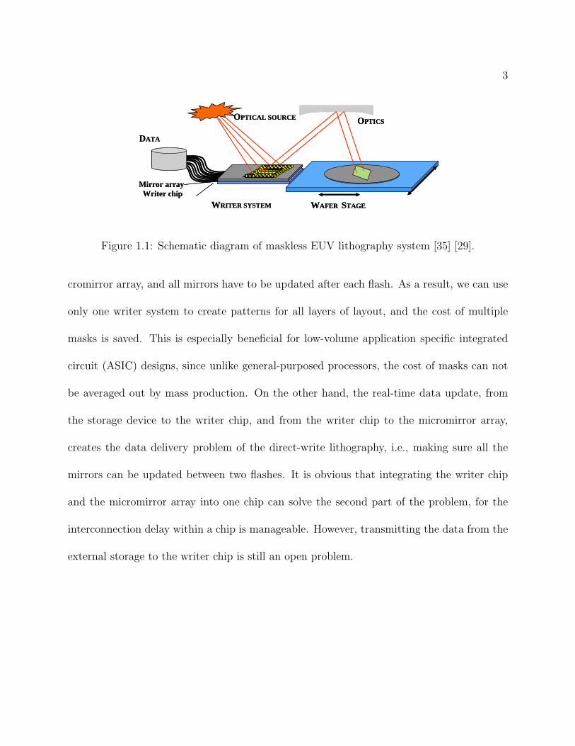
1.2 The Architecture of Maskless Lithography Systems
Figure 1.1 shows the architecture of an optical maskless lithography system [35] [29]. A
similar architecture for the E-beam lithography can be found in the literature [33]. In this
architecture, the optical source flashes on a writer system, which consists of a micromirror
array and a writer control chip underneath it, and the patterns on the mirror array are
reflected to the wafer on the scanning wafer stage. As the stage moves, the writer system
has to provide different layout patterns for different portions of the wafer, and the data
is transmitted from external storage devices to the writer system. Due to the physical
dimension constraints of the micromirror array and writer system, an entire wafer can be
written in a few thousands of such flashes.
In this scenario, the writer system controls the movement of every mirror in the mi-
3
DATA
WRITER SYSTEM WAFER STAGE
OPTICSOPTICAL SOURCE
Mirror arrayWriter chip
DATA
WRITER SYSTEM WAFER STAGE
OPTICSOPTICAL SOURCE
Mirror arrayWriter chip
Figure 1.1: Schematic diagram of maskless EUV lithography system [35] [29].
cromirror array, and all mirrors have to be updated after each flash. As a result, we can use
only one writer system to create patterns for all layers of layout, and the cost of multiple
masks is saved. This is especially beneficial for low-volume application specific integrated
circuit (ASIC) designs, since unlike general-purposed processors, the cost of masks can not
be averaged out by mass production. On the other hand, the real-time data update, from
the storage device to the writer chip, and from the writer chip to the micromirror array,
creates the data delivery problem of the direct-write lithography, i.e., making sure all the
mirrors can be updated between two flashes. It is obvious that integrating the writer chip
and the micromirror array into one chip can solve the second part of the problem, for the
interconnection delay within a chip is manageable. However, transmitting the data from the
external storage to the writer chip is still an open problem.
4
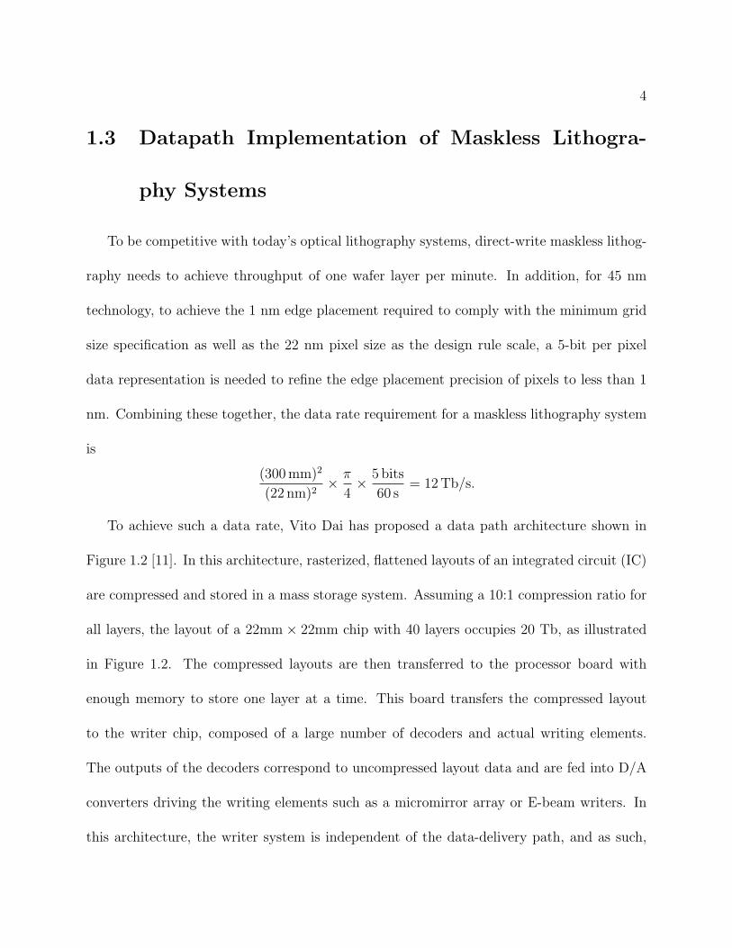
1.3 Datapath Implementation of Maskless Lithogra-
phy Systems
To be competitive with today’s optical lithography systems, direct-write maskless lithog-
raphy needs to achieve throughput of one wafer layer per minute. In addition, for 45 nm
technology, to achieve the 1 nm edge placement required to comply with the minimum grid
size specification as well as the 22 nm pixel size as the design rule scale, a 5-bit per pixel
data representation is needed to refine the edge placement precision of pixels to less than 1
nm. Combining these together, the data rate requirement for a maskless lithography system
is
(300mm)2
(22 nm)2× �
4× 5 bits
60 s= 12Tb/s.
To achieve such a data rate, Vito Dai has proposed a data path architecture shown in
Figure 1.2 [11]. In this architecture, rasterized, flattened layouts of an integrated circuit (IC)
are compressed and stored in a mass storage system. Assuming a 10:1 compression ratio for
all layers, the layout of a 22mm × 22mm chip with 40 layers occupies 20 Tb, as illustrated
in Figure 1.2. The compressed layouts are then transferred to the processor board with
enough memory to store one layer at a time. This board transfers the compressed layout
to the writer chip, composed of a large number of decoders and actual writing elements.
The outputs of the decoders correspond to uncompressed layout data and are fed into D/A
converters driving the writing elements such as a micromirror array or E-beam writers. In
this architecture, the writer system is independent of the data-delivery path, and as such,
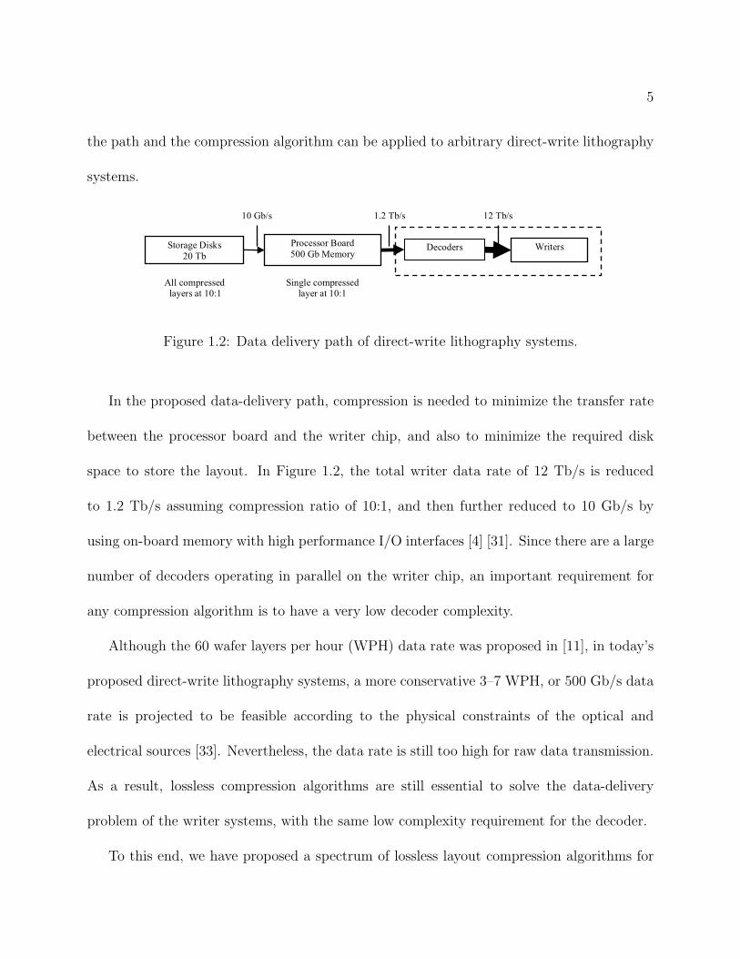
5
the path and the compression algorithm can be applied to arbitrary direct-write lithography
systems.
Storage Disks
20 Tb
All compressed layers at 10:1
10 Gb/s
Decoders Writers
12 Tb/s
Processor Board
500 Gb Memory
1.2 Tb/s
Single compressed layer at 10:1
Figure 1.2: Data delivery path of direct-write lithography systems.
In the proposed data-delivery path, compression is needed to minimize the transfer rate
between the processor board and the writer chip, and also to minimize the required disk
space to store the layout. In Figure 1.2, the total writer data rate of 12 Tb/s is reduced
to 1.2 Tb/s assuming compression ratio of 10:1, and then further reduced to 10 Gb/s by
using on-board memory with high performance I/O interfaces [4] [31]. Since there are a large
number of decoders operating in parallel on the writer chip, an important requirement for
any compression algorithm is to have a very low decoder complexity.
Although the 60 wafer layers per hour (WPH) data rate was proposed in [11], in today’s
proposed direct-write lithography systems, a more conservative 3–7 WPH, or 500 Gb/s data
rate is projected to be feasible according to the physical constraints of the optical and
electrical sources [33]. Nevertheless, the data rate is still too high for raw data transmission.
As a result, lossless compression algorithms are still essential to solve the data-delivery
problem of the writer systems, with the same low complexity requirement for the decoder.
To this end, we have proposed a spectrum of lossless layout compression algorithms for
6
flattened, rasterized data within the family of context-copy-combinatorial-code (C4), which
have been shown to outperform all existing techniques such as BZIP2, 2D-LZ, and LZ77
in terms of compression efficiency, especially under limited decoder buffer size, as required
for hardware implementation. However, the results shown in [27] and [10] only proved the
simplicity of the software decoding. The remaining question is: can those lossless compression
algorithms be implemented in hardware and ultimately be integrated into the writer chip
with a minimal amount of overhead? This is the main question I answer in this thesis.
1.4 Related Work on Maskless Lithography
Although the research on direct-write maskless lithography has been on going for a
decade, the main research focus is still on developing a prototype system. Table 1.1 lists
a sample of on going electron-beam maskless lithography projects in Europe and United
States [34] [33]. The schematics of MAPPER, projection maskless lithography (PML2), and
Vistec systems are shown in Figures 1.3, 1.4, and 1.5 respectively. Although these three
systems have different energy levels, current densities, and beam splitting mechanisms, they
all adapt the architecture from scanning electron microscope (SEM), where the electron gun
is placed on top, followed by patterning mechanism, condenser lens, and wafer. On the other
hand, reflective E-beam lithography (REBL) places the patterning device, i.e., digital pat-
tern generator (DPG) on the side, and bends the E-beam using a magnetic field, as shown in
Figure 1.6. In spite of the differences among the system architectures, the patterning devices
in these systems have to be updated dynamically to create layout patterns for different por-
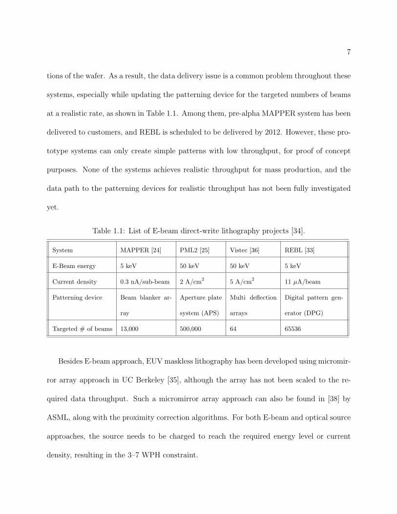
7
tions of the wafer. As a result, the data delivery issue is a common problem throughout these
systems, especially while updating the patterning device for the targeted numbers of beams
at a realistic rate, as shown in Table 1.1. Among them, pre-alpha MAPPER system has been
delivered to customers, and REBL is scheduled to be delivered by 2012. However, these pro-
totype systems can only create simple patterns with low throughput, for proof of concept
purposes. None of the systems achieves realistic throughput for mass production, and the
data path to the patterning devices for realistic throughput has not been fully investigated
yet.
Table 1.1: List of E-beam direct-write lithography projects [34].
System MAPPER [24] PML2 [25] Vistec [36] REBL [33]
E-Beam energy 5 keV 50 keV 50 keV 5 keV
Current density 0.3 nA/sub-beam 2 A/cm2
5 A/cm2
11 �A/beam
Patterning device Beam blanker ar-
ray
Aperture plate
system (APS)
Multi deflection
arrays
Digital pattern gen-
erator (DPG)
Targeted # of beams 13,000 500,000 64 65536
Besides E-beam approach, EUV maskless lithography has been developed using micromir-
ror array approach in UC Berkeley [35], although the array has not been scaled to the re-
quired data throughput. Such a micromirror array approach can also be found in [38] by
ASML, along with the proximity correction algorithms. For both E-beam and optical source
approaches, the source needs to be charged to reach the required energy level or current
density, resulting in the 3–7 WPH constraint.
8
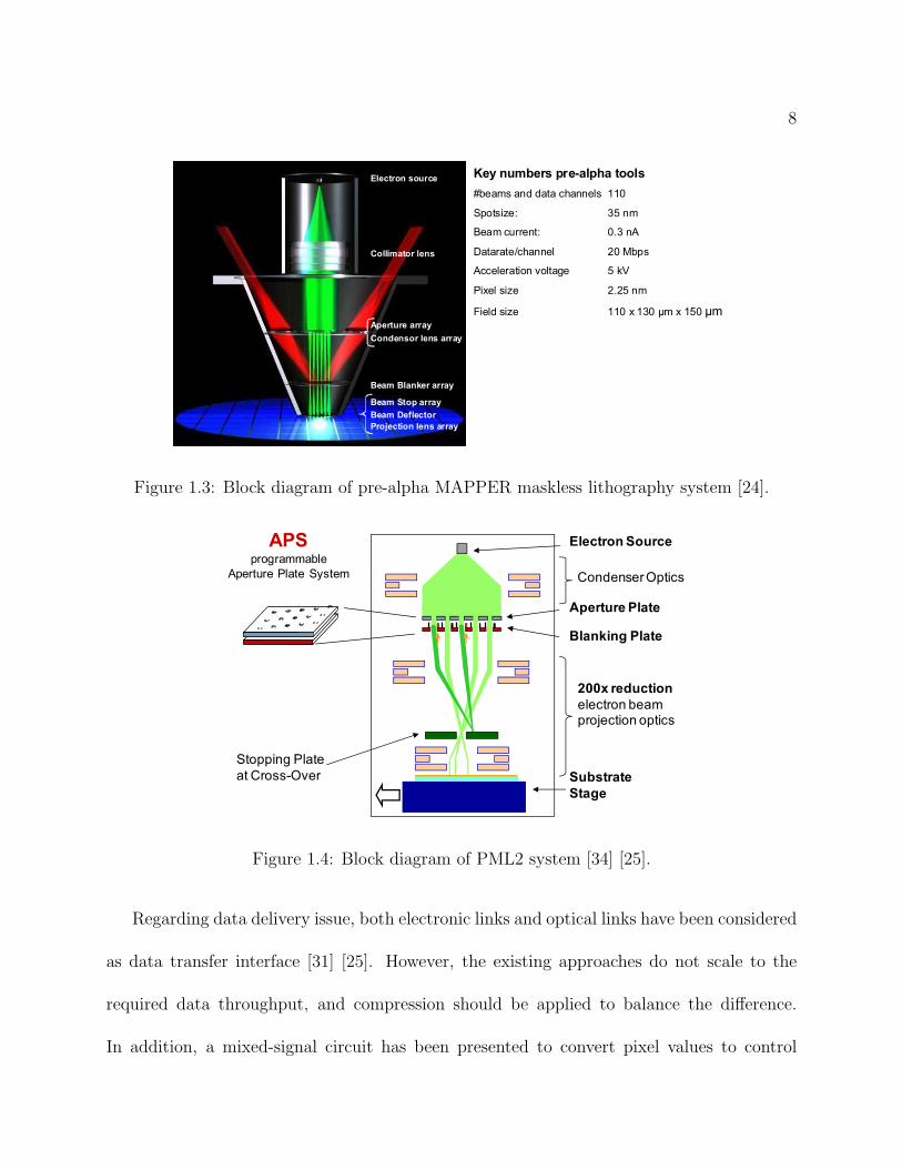
Key numbers pre-alpha tools
#beams and data channels 110
Spotsize: 35 nm
Beam current: 0.3 nA
Datarate/channel 20 Mbps
Acceleration voltage 5 kV
Pixel size 2.25 nm
Field size 110 x 130 µm x 150 µm
Electron source
Collimator lens
Aperture array
Beam Blanker array
Beam Deflector array
Projection lens array
Condensor lens array
Beam Stop array
Projection lens array
Electron source
Collimator lens
Aperture array
Beam Blanker array
Beam Deflector
Condensor lens array
Beam Stop array
Figure 1.3: Block diagram of pre-alpha MAPPER maskless lithography system [24].
Stopping Plate
at Cross-Over Substrate
Stage
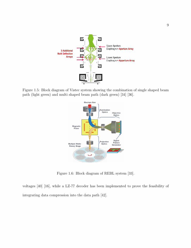
APSprogrammable
Aperture Plate System
200x reduction
electron beam projection optics
Electron Source
Condenser Optics
Aperture Plate
Blanking Plate
Figure 1.4: Block diagram of PML2 system [34] [25].
Regarding data delivery issue, both electronic links and optical links have been considered
as data transfer interface [31] [25]. However, the existing approaches do not scale to the
required data throughput, and compression should be applied to balance the difference.
In addition, a mixed-signal circuit has been presented to convert pixel values to control
9
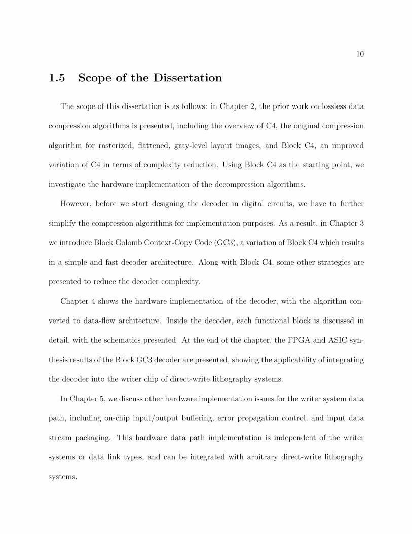
Figure 1.5: Block diagram of Vistec system showing the combination of single shaped beampath (light green) and multi shaped beam path (dark green) [34] [36].
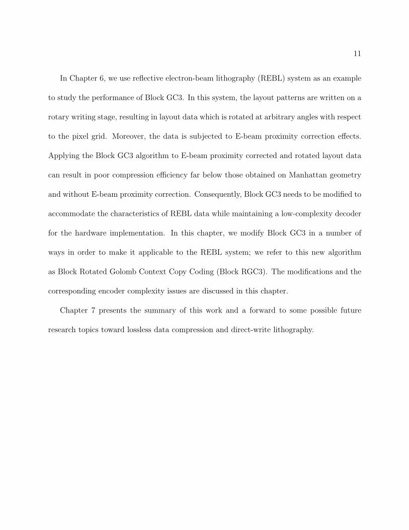
Figure 1.6: Block diagram of REBL system [33].
voltages [40] [16], while a LZ-77 decoder has been implemented to prove the feasibility of
integrating data compression into the data path [42].
10
1.5 Scope of the Dissertation
The scope of this dissertation is as follows: in Chapter 2, the prior work on lossless data
compression algorithms is presented, including the overview of C4, the original compression
algorithm for rasterized, flattened, gray-level layout images, and Block C4, an improved
variation of C4 in terms of complexity reduction. Using Block C4 as the starting point, we
investigate the hardware implementation of the decompression algorithms.
However, before we start designing the decoder in digital circuits, we have to further
simplify the compression algorithms for implementation purposes. As a result, in Chapter 3
we introduce Block Golomb Context-Copy Code (GC3), a variation of Block C4 which results
in a simple and fast decoder architecture. Along with Block C4, some other strategies are
presented to reduce the decoder complexity.
Chapter 4 shows the hardware implementation of the decoder, with the algorithm con-
verted to data-flow architecture. Inside the decoder, each functional block is discussed in
detail, with the schematics presented. At the end of the chapter, the FPGA and ASIC syn-
thesis results of the Block GC3 decoder are presented, showing the applicability of integrating
the decoder into the writer chip of direct-write lithography systems.
In Chapter 5, we discuss other hardware implementation issues for the writer system data
path, including on-chip input/output buffering, error propagation control, and input data
stream packaging. This hardware data path implementation is independent of the writer
systems or data link types, and can be integrated with arbitrary direct-write lithography
systems.
11
In Chapter 6, we use reflective electron-beam lithography (REBL) system as an example
to study the performance of Block GC3. In this system, the layout patterns are written on a
rotary writing stage, resulting in layout data which is rotated at arbitrary angles with respect
to the pixel grid. Moreover, the data is subjected to E-beam proximity correction effects.
Applying the Block GC3 algorithm to E-beam proximity corrected and rotated layout data
can result in poor compression efficiency far below those obtained on Manhattan geometry
and without E-beam proximity correction. Consequently, Block GC3 needs to be modified to
accommodate the characteristics of REBL data while maintaining a low-complexity decoder
for the hardware implementation. In this chapter, we modify Block GC3 in a number of
ways in order to make it applicable to the REBL system; we refer to this new algorithm
as Block Rotated Golomb Context Copy Coding (Block RGC3). The modifications and the
corresponding encoder complexity issues are discussed in this chapter.
Chapter 7 presents the summary of this work and a forward to some possible future
research topics toward lossless data compression and direct-write lithography.
12
Chapter 2
Prior Work on Lossless Data
Compression Algorithms for Maskless
Lithography Systems
In the proposed data-delivery path in Chapter 1, compression is needed to minimize the
transfer rate between the processor board and the writer chip, and also to minimize the
required disk space to store the layout data. Since there are a large number of decoders
operating in parallel on the writer chip to achieve the projected output data rate, an impor-
tant requirement for any compression algorithm is to have an extremely low decompression
complexity. To this end, Vito Dai and I have proposed a series of lossless layout compression
algorithms for flattened, rasterized data [14] [27]. In this chapter, the previous work on
lossless layout image compression is reviewed. In particular, the family of Context Copy
13
Combinatorial Code (C4) compression algorithms are introduced in detail.
2.1 Overview of C4
While observing the flattened, layout images, we can notice two prominent character-
istics: Manhattan shape of the patterns, and repetitiveness of the patterns, as shown in
Figure 2.1. Moreover, layout images consist of only monotone foreground (layout patterns)
and background. By denoting foreground pixels as “1”s and background pixels as “0”s,
the layout images can be represented in binary level, with the pixel grid equals the edge
placement grid. In such a case, bi-level context prediction, e.g., JBIG, can be applied to
predict the Manhattan patterns [1] [11]. On the other hand, for the repetitive patterns, a
2-dimensional Lemple-Ziv style copying method was developed to achieve compression effi-
ciency [48] [9]. However, if we consider the pixel size as the design rule scale, i.e., half of the
minimum feature size, and 1 nm edge placement as in GDS file specifications, such a binary
image model no longer sustains, and the layout image must be represented in gray scale by
applying rasterization [12]. To compress such flattened, rasterized gray-level layout images,
new lossless image compression algorithm is needed.
To compress the images efficiently, we must utilize both characteristics by either predict-
ing the pixel value from its neighborhood to preserve the horizontal and vertical edges of
the patterns, or copying the patterns directly from the buffer to exploit the repetition of
the data. The family of Context Copy Combinatorial Code (C4) compression algorithms
combines those two techniques, local context-based prediction [41] and Lempel-Ziv (LZ)
14
(a) (b)
Figure 2.1: (a)Repetitive and (b) non-repetitive layouts.
style copying, to achieve lossless compression for the rasterized layout images. In other
words, the encoder divides the layout images into “predict” and “copy” regions, which are
non-overlapping rectangles, and only the residues from the prediction and copy operations
are transmitted to the decoder. By avoiding redundant transmission of copied or predicted
pixels, C4 achieves high compression efficiency.
Figure 2.2 shows a high-level block diagram of the C4 encoder and decoder for flattened,
rasterized gray-level layout images. First, a prediction error image is generated from the
layout, using a simple three-pixel prediction model to be described shortly. Next, the “Find
copy regions” block uses the error image to segment the layout image automatically, i.e.,
generate a segmentation map between copy and predict regions. As specified by the segmen-
tation, the predict/copy block estimates each pixel value, either by copying or by prediction.
The result is compared to the actual value in the layout image. Correct pixel values are in-
dicated with a “0” and incorrect values are indicated with a “1.” The pixel error location is
compressed without loss by the hierarchical combinatorial code (HCC) encoder [13] [14], and
15
the corresponding pixel error value is compressed by the Huffman encoder. These compressed
bit streams are transmitted to the decoder, along with the segmentation map, indicating the
copy and predict regions of the layout images.
compressed
error value
error location map
error value
Compute prediction
error image
Find copy
regions Layout
segmentationPredict/Copy
Compare
HCC Decoder
Predict/Copy
Layout Buffer
Merge
HCC Encoder
Decoder
Huffman Encoder
Huffman Decodererror location maperror value
compressed
error location map
Encoder
Figure 2.2: Block diagram of C4 encoder and decoder for gray-level images.
The decoder mirrors the encoder, but skips the complex process necessary to find the seg-
mentation map, which is directly received from the encoder. The HCC decoder decompresses
the error location bits from the encoder. As specified by the segmentation, the Predict/Copy
block estimates each pixel value, either by copying or by prediction. If the error location bit
is “0”, the pixel value is correct, and if the error location bit is “1”, the pixel value is incor-
rect, and must be replaced by the actual pixel value decoded from Huffman decoder. There
is no segmentation performed in the C4 decoder, so it is considerably simpler to implement
than the encoder.
Linear prediction is used in C4, where each pixel is predicted from its three-pixel neigh-
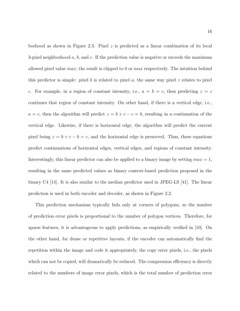
16
borhood as shown in Figure 2.3. Pixel z is predicted as a linear combination of its local
3-pixel neighborhood a, b, and c. If the prediction value is negative or exceeds the maximum
allowed pixel value max, the result is clipped to 0 or max respectively. The intuition behind
this predictor is simple: pixel b is related to pixel a, the same way pixel z relates to pixel
c. For example, in a region of constant intensity, i.e., a = b = c, then predicting z = c
continues that region of constant intensity. On other hand, if there is a vertical edge, i.e.,
a = c, then the algorithm will predict z = b + c − c = b, resulting in a continuation of the
vertical edge. Likewise, if there is horizontal edge, the algorithm will predict the current
pixel being z = b + c − b = c, and the horizontal edge is preserved. Thus, these equations
predict continuations of horizontal edges, vertical edges, and regions of constant intensity.
Interestingly, this linear predictor can also be applied to a binary image by setting max = 1,
resulting in the same predicted values as binary context-based prediction proposed in the
binary C4 [14]. It is also similar to the median predictor used in JPEG-LS [41]. The linear
prediction is used in both encoder and decoder, as shown in Figure 2.2.
This prediction mechanism typically fails only at corners of polygons, so the number
of prediction error pixels is proportional to the number of polygon vertices. Therefore, for
sparse features, it is advantageous to apply predictions, as empirically verified in [10]. On
the other hand, for dense or repetitive layouts, if the encoder can automatically find the
repetition within the image and code it appropriately, the copy error pixels, i.e., the pixels
which can not be copied, will dramatically be reduced. The compression efficiency is directly
related to the numbers of image error pixels, which is the total number of prediction error
17
pixels and copy error pixels. In C4, the major task is to develop an automatic algorithm to
minimize the number of image error pixels.
a b
c z
x = b – a + cif (x < 0) then z = 0 if (x > max) then z = max
otherwise z = x
Figure 2.3: Three-pixel linear prediction with saturation in C4.
It is obvious that the segmentation operation in the C4 encoder is extremely computa-
tionally intensive, and is vital to the compression efficiency of C4. In fact, a greedy heuristics
search algorithm is applied in C4, resulting in the best compression efficiency as compared
to all existed lossless compression algorithms [14]; however, the encoding time of C4 is also
larger than other algorithms. To reduce this computational overhead, a variant of C4, called
Block C4, is developed.
2.2 Block C4
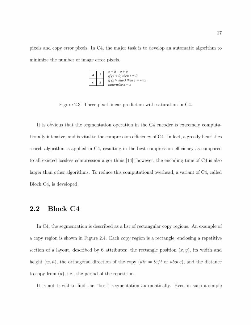
In C4, the segmentation is described as a list of rectangular copy regions. An example of
a copy region is shown in Figure 2.4. Each copy region is a rectangle, enclosing a repetitive
section of a layout, described by 6 attributes: the rectangle position (x, y), its width and
height (w, ℎ), the orthogonal direction of the copy (dir = left or above), and the distance
to copy from (d), i.e., the period of the repetition.
It is not trivial to find the “best” segmentation automatically. Even in such a simple
18
w
h
d (x,y)
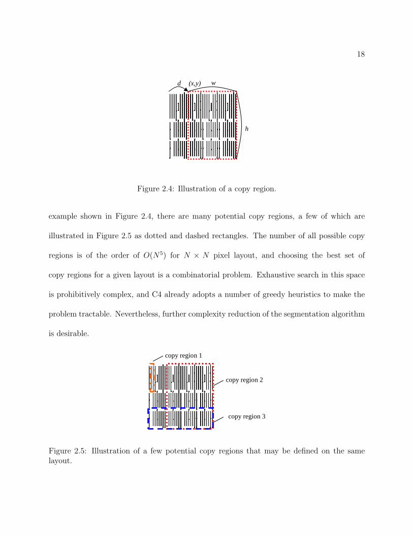
Figure 2.4: Illustration of a copy region.
example shown in Figure 2.4, there are many potential copy regions, a few of which are
illustrated in Figure 2.5 as dotted and dashed rectangles. The number of all possible copy
regions is of the order of O(N5) for N × N pixel layout, and choosing the best set of
copy regions for a given layout is a combinatorial problem. Exhaustive search in this space
is prohibitively complex, and C4 already adopts a number of greedy heuristics to make the
problem tractable. Nevertheless, further complexity reduction of the segmentation algorithm
is desirable.
copy region 1
copy region 2
copy region 3
Figure 2.5: Illustration of a few potential copy regions that may be defined on the samelayout.
19
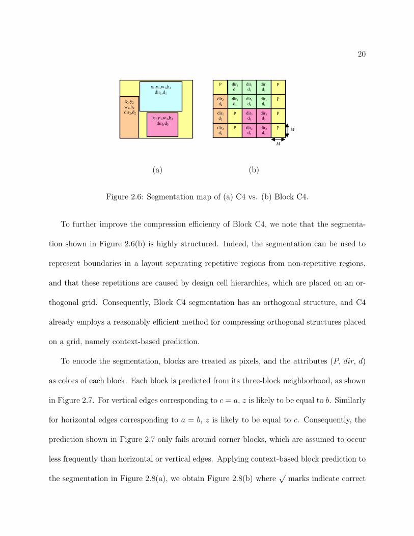
Block C4 adopts a far more restrictive segmentation algorithm than C4, and as such,
is much faster to compute. Specifically, Block C4 restricts both the position and sizes to
fixed M ×M blocks on a grid whereas C4 allows for copy regions to be placed in arbitrary
(x, y) positions with arbitrary (w, ℎ) sizes. Figure 2.6 illustrates the difference between
Block C4 and C4 segmentations. In Figure 2.6(a), the segmentation for C4 is composed of 3
rectangular copy regions, with 6 attributes (x, y, w, ℎ, dir, d) describing each copy region.
In Figure 2.6(b), the segmentation for Block C4 is composed of twenty M ×M tiles, with
each tile marked as either prediction (P ), or copy with direction and distance (dir, d). This
simple change reduces the number of possible copy regions to
O
(
N3
M2
)
≈ N2
M2×O(N),
a substantial N2M2 reduction in search space compared to C4. For our test data, N = 1024
and M = 8, so the copy region search space has been reduced by a factor of 64 million.
However, this complexity reduction could potentially come at the expense of compression
efficiency, as illustrated in Section 2.3.
The complexity reduction is also a function of the block size M , where the smaller the
block size, the better approximation of Figure 2.6(a) by Figure 2.6(b). In this case, Block
C4 and C4 result in the same segmentation map, hence the same number of image errors.
However, in this scenario, the segmentation map of Block C4 is broken down to too many
tiles, and transmitting the segmentation information becomes a challenge for the encoder. To
balance these two effects, We have empirically found M = 8 to exhibit the best compression
efficiency for nearly all test cases as compared to M = 4 or M = 16.
20
x1,y1,w1,h1
dir1,d1
x3,y3,w3,h3
dir3,d3
x2,y2
w2,h2
dir2,d2
dir1
d1
,2dir2
d2
P
dir2
d2
dir2
d2
dir1
d1
dir1
d1
dir1
d1
dir1
d1
dir1
d1
P
P
dir3
d3
dir3
d3
dir3
d3
dir3
d3
P
P
P
P
M
M
(a) (b)
Figure 2.6: Segmentation map of (a) C4 vs. (b) Block C4.
To further improve the compression efficiency of Block C4, we note that the segmenta-
tion shown in Figure 2.6(b) is highly structured. Indeed, the segmentation can be used to
represent boundaries in a layout separating repetitive regions from non-repetitive regions,
and that these repetitions are caused by design cell hierarchies, which are placed on an or-
thogonal grid. Consequently, Block C4 segmentation has an orthogonal structure, and C4
already employs a reasonably efficient method for compressing orthogonal structures placed
on a grid, namely context-based prediction.
To encode the segmentation, blocks are treated as pixels, and the attributes (P, dir, d)
as colors of each block. Each block is predicted from its three-block neighborhood, as shown
in Figure 2.7. For vertical edges corresponding to c = a, z is likely to be equal to b. Similarly
for horizontal edges corresponding to a = b, z is likely to be equal to c. Consequently, the
prediction shown in Figure 2.7 only fails around corner blocks, which are assumed to occur
less frequently than horizontal or vertical edges. Applying context-based block prediction to
the segmentation in Figure 2.8(a), we obtain Figure 2.8(b) where√
marks indicate correct
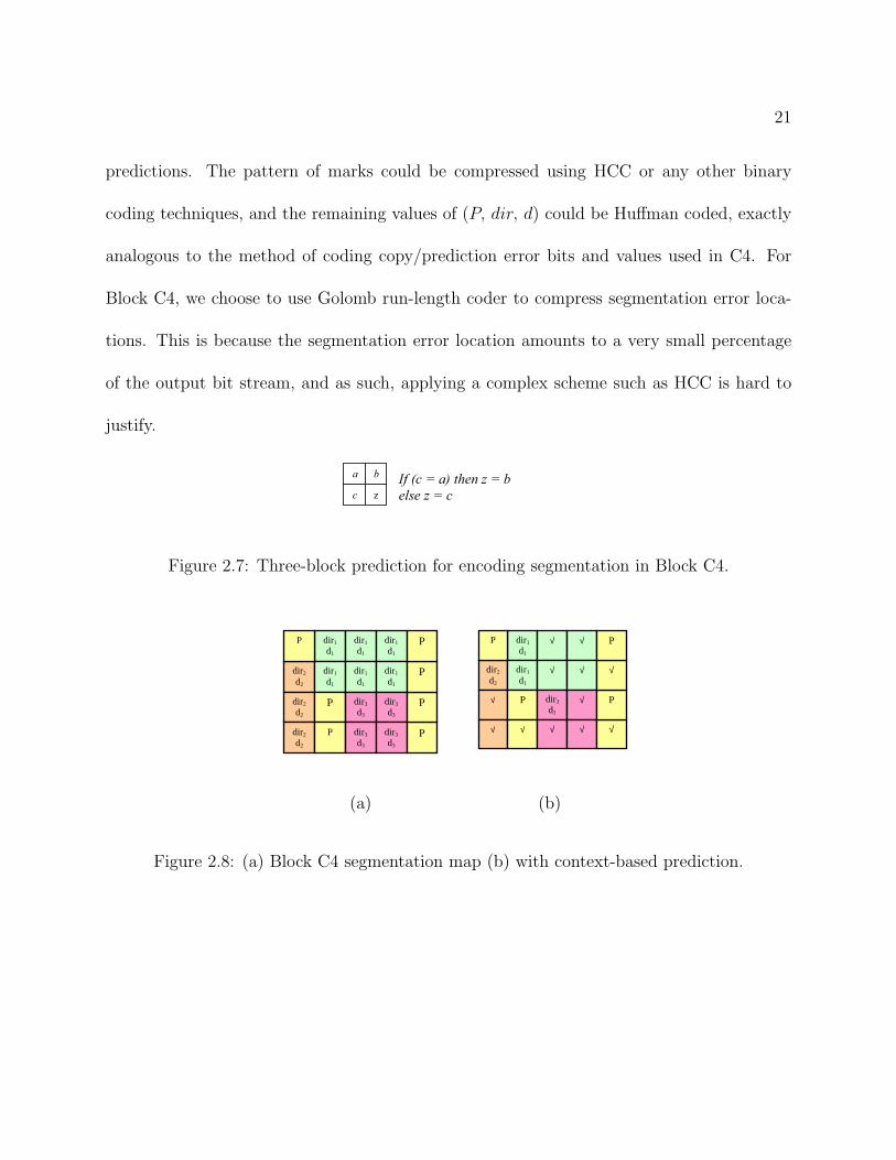
21
predictions. The pattern of marks could be compressed using HCC or any other binary
coding techniques, and the remaining values of (P, dir, d) could be Huffman coded, exactly
analogous to the method of coding copy/prediction error bits and values used in C4. For
Block C4, we choose to use Golomb run-length coder to compress segmentation error loca-
tions. This is because the segmentation error location amounts to a very small percentage
of the output bit stream, and as such, applying a complex scheme such as HCC is hard to
justify.
a b
c z
If (c = a) then z = b
else z = c
Figure 2.7: Three-block prediction for encoding segmentation in Block C4.
dir1
d1
,2dir2
d2
P
dir2
d2
dir2
d2
dir1
d1
dir1
d1
dir1
d1
dir1
d1
dir1
d1
P
P
dir3
d3
dir3
d3
dir3
d3
dir3
d3
P
P
P
P
,2
dir1
d1
,2dir2
d2
P
√
√
√ √
dir1
d1
√ √
P
√
dir3
d3
√
√
√ √
P
√
P
(a) (b)
Figure 2.8: (a) Block C4 segmentation map (b) with context-based prediction.
22
2.3 Compression Efficiency Results
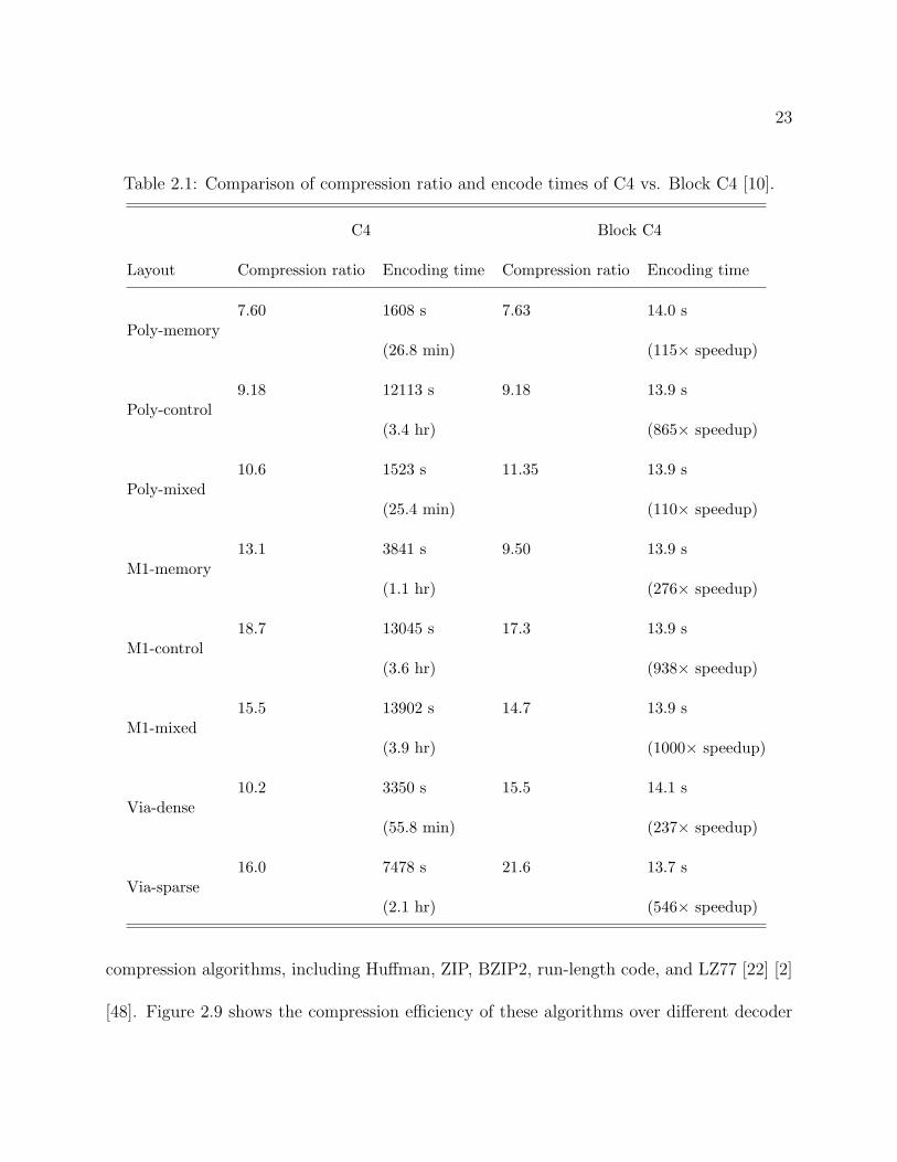
The full table of results, comparing Block C4 to C4 is shown in Table 2.1 [10]. In it, we
compare the compression efficiency and encoding time of various 1024×1024 5-bit gray-scale
images, generated from different sections and layers of an industry microchip. In columns,
from left to right, are the layer image name, C4 compression ratio, C4 encode time, Block
C4 compression ratio, and Block C4 encode time. Both C4 and Block C4 use the smallest
1.7 KB buffer, corresponding to only 2 stored rows of data. Encoding times are generated
on an AMD Athlon64TM 3200+ Windows XP desktop with 1 GB of memory.
A quick glance at this table makes it clear that the speed advantage of Block C4 over
C4 is universal, i.e., over 100 times faster than C4, and consistent, i.e., 13.7 to 14.1 seconds,
for all layers and layout types tested. In general, the compression efficiency of Block C4
matches that of C4. One exception is row 5 of Table 2.1, where C4 exceeds the compression
efficiency of Block C4, on the highly regular M1-memory layout.
For this layout, C4’s compression ratio is 13.1, while Block C4’s compression ratio is
9.5. In this particular case, the layout is extremely repetitive, and C4 covers 99% of the
entire 1024× 1024 image with only 132 copy regions. Moreover, many of these copy regions
are long narrow strips, less than 8-pixels wide, which Block C4 cannot possibly duplicate.
Consequently, Block C4 exhibits a loss of compression efficiency as compared to C4, in this
particular case. Reducing the block size of Block C4 may potentially improve the compression
efficiency, since C4 can be treated as a special case of Block C4 with the block size of 1× 1.
The other comparison is performed among, C4, Block C4, and other existing lossless
23
Table 2.1: Comparison of compression ratio and encode times of C4 vs. Block C4 [10].
C4 Block C4
Layout Compression ratio Encoding time Compression ratio Encoding time
Poly-memory7.60 1608 s 7.63 14.0 s
(26.8 min) (115× speedup)
Poly-control9.18 12113 s 9.18 13.9 s
(3.4 hr) (865× speedup)
Poly-mixed10.6 1523 s 11.35 13.9 s
(25.4 min) (110× speedup)
M1-memory13.1 3841 s 9.50 13.9 s
(1.1 hr) (276× speedup)
M1-control18.7 13045 s 17.3 13.9 s
(3.6 hr) (938× speedup)
M1-mixed15.5 13902 s 14.7 13.9 s
(3.9 hr) (1000× speedup)
Via-dense10.2 3350 s 15.5 14.1 s
(55.8 min) (237× speedup)
Via-sparse16.0 7478 s 21.6 13.7 s
(2.1 hr) (546× speedup)
compression algorithms, including Huffman, ZIP, BZIP2, run-length code, and LZ77 [22] [2]
[48]. Figure 2.9 shows the compression efficiency of these algorithms over different decoder
24
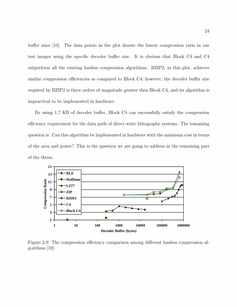
buffer sizes [10]. The data points in the plot denote the lowest compression ratio in our
test images using the specific decoder buffer size. It is obvious that Block C4 and C4
outperform all the existing lossless compression algorithms. BZIP2, in this plot, achieves
similar compression efficiencies as compared to Block C4; however, the decoder buffer size
required by BZIP2 is three orders of magnitude greater then Block C4, and its algorithm is
impractical to be implemented in hardware.
By using 1.7 KB of decoder buffer, Block C4 can successfully satisfy the compression
efficiency requirement for the data path of direct-write lithography systems. The remaining
question is: Can this algorithm be implemented in hardware with the minimum cost in terms
of the area and power? This is the question we are going to address in the remaining part
of the thesis.
1
3
5
7
9
11
13
15
1 10 100 1000 10000 100000 1000000
Decoder Buffer (bytes)
Com
pres
sion
Rat
io
RLE
Huffman
LZ77
ZIP
BZIP2
C4
Block C4
Figure 2.9: The compression efficiency comparison among different lossless compression al-gorithms [10].
25
Chapter 3
Block GC3 Lossless Compression
Algorithm
3.1 Introduction
Before we start designing the decoder in digital circuits, we have to further simplify the
compression algorithms for implementation purposes. Specifically, we have to reduce the
number of data streams, and ensure parallelism of the decoding architecture. In software
decoding, since the instructions are executed sequentially, results from the previous func-
tions are naturally ready for the current operation. However, in hardware, such sequential
operation is controlled by a state machine, and often results in a low throughput or a com-
plicated design. In this chapter, we modify Block C4 algorithmically to avoid sequential
decoding, along with some other optimization strategies. The resulting algorithm, Block
26
Golomb Context-Copy Code (GC3), is discussed in detail in the remainder of the chapter.
3.2 Block GC3
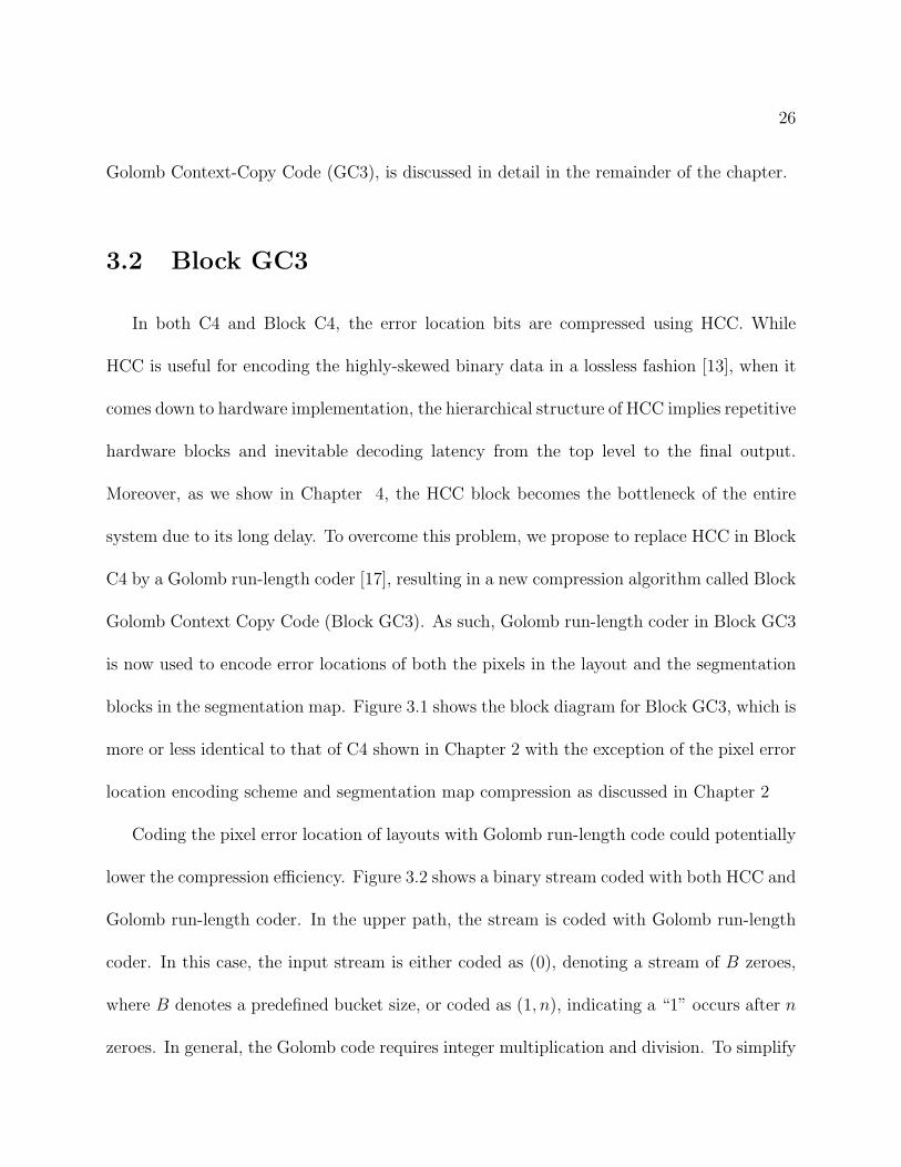
In both C4 and Block C4, the error location bits are compressed using HCC. While
HCC is useful for encoding the highly-skewed binary data in a lossless fashion [13], when it
comes down to hardware implementation, the hierarchical structure of HCC implies repetitive
hardware blocks and inevitable decoding latency from the top level to the final output.
Moreover, as we show in Chapter 4, the HCC block becomes the bottleneck of the entire
system due to its long delay. To overcome this problem, we propose to replace HCC in Block
C4 by a Golomb run-length coder [17], resulting in a new compression algorithm called Block
Golomb Context Copy Code (Block GC3). As such, Golomb run-length coder in Block GC3
is now used to encode error locations of both the pixels in the layout and the segmentation
blocks in the segmentation map. Figure 3.1 shows the block diagram for Block GC3, which is
more or less identical to that of C4 shown in Chapter 2 with the exception of the pixel error
location encoding scheme and segmentation map compression as discussed in Chapter 2
Coding the pixel error location of layouts with Golomb run-length code could potentially
lower the compression efficiency. Figure 3.2 shows a binary stream coded with both HCC and
Golomb run-length coder. In the upper path, the stream is coded with Golomb run-length
coder. In this case, the input stream is either coded as (0), denoting a stream of B zeroes,
where B denotes a predefined bucket size, or coded as (1, n), indicating a “1” occurs after n
zeroes. In general, the Golomb code requires integer multiplication and division. To simplify
27
Layout
Compare Golomb RLE
segmentation values
image error map
image error values
Predict/Copy
Merge
Golomb RLD
Layout/Buffer
image error map
image error values
Encoder
Decoder
Region Encoder
Region Decoder
Find Best Copy Distance
Predict/Copy Golomb RLE
Huffman Encoder
Huffman Decoder
Golomb RLD
seg. error values
seg. error map
seg. error map
Figure 3.1: The encoder/decoder architecture of Block GC3.
it to bit-shifting operation, we restrict B to be power of 2. These parameters are further
converted into a bit stream, where parameter (0) is translated into a 1-bit codeword, and
(1, n) takes 1+log2 B bits to encode. Therefore, a stream with successive ones can potentially
be encoded into a longer code than a stream with ones which are far apart from each other.
On the other hand, in the lower path of Figure 3.2, HCC counts the number of ones within
a fixed block size and codes it using enumerative code [14]. In Figure 3.2, the block size is 8
and attributes (2, 11) denote the 11tℎ greatest 8-bit sequence with two “1”s, i.e., “01000010.”
The attributes (2, 11) are further translated to codewords “010” and “01011,” which are the
binary representations of 2 and 11 respectively. As long as the number of ones inside the
block is fixed, HCC results in a fixed length bit stream regardless of the input distribution.
Based on the above, Block GC3 can result in potential compression efficiency loss for
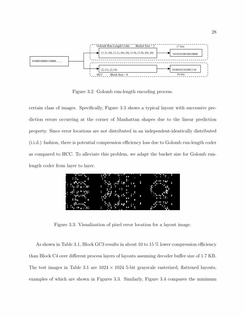
28
0100010000110000……
(1,1), (0), (1,1), (0), (0), (1.0), (1.0), (0), (0)
(2,11), (2,14)
10101010010010000
0100101101001110
Golomb Run-Length Coder Bucket Size = 2
16 bits
17 bits
HCC Block Size = 8
Figure 3.2: Golomb run-length encoding process.
certain class of images. Specifically, Figure 3.3 shows a typical layout with successive pre-
diction errors occurring at the corner of Manhattan shapes due to the linear prediction
property. Since error locations are not distributed in an independent-identically distributed
(i.i.d.) fashion, there is potential compression efficiency loss due to Golomb run-length coder
as compared to HCC. To alleviate this problem, we adapt the bucket size for Golomb run-
length coder from layer to layer.
Figure 3.3: Visualization of pixel error location for a layout image.
As shown in Table 3.1, Block GC3 results in about 10 to 15 % lower compression efficiency
than Block C4 over different process layers of layouts assuming decoder buffer size of 1.7 KB.
The test images in Table 3.1 are 1024 × 1024 5-bit grayscale rasterized, flattened layouts,
examples of which are shown in Figures 3.3. Similarly, Figure 3.4 compares the minimum
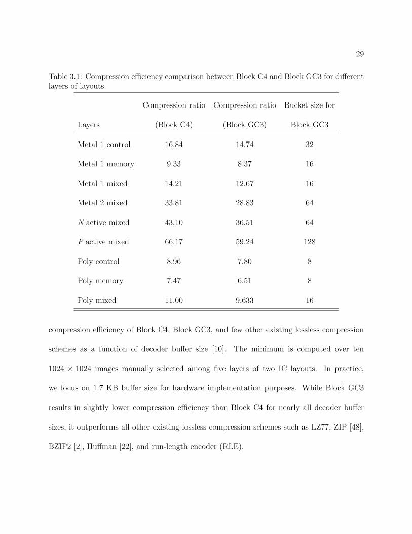
29
Table 3.1: Compression efficiency comparison between Block C4 and Block GC3 for differentlayers of layouts.
Compression ratio Compression ratio Bucket size for
Layers (Block C4) (Block GC3) Block GC3
Metal 1 control 16.84 14.74 32
Metal 1 memory 9.33 8.37 16
Metal 1 mixed 14.21 12.67 16
Metal 2 mixed 33.81 28.83 64
N active mixed 43.10 36.51 64
P active mixed 66.17 59.24 128
Poly control 8.96 7.80 8
Poly memory 7.47 6.51 8
Poly mixed 11.00 9.633 16
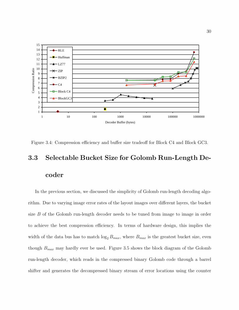
compression efficiency of Block C4, Block GC3, and few other existing lossless compression
schemes as a function of decoder buffer size [10]. The minimum is computed over ten
1024 × 1024 images manually selected among five layers of two IC layouts. In practice,
we focus on 1.7 KB buffer size for hardware implementation purposes. While Block GC3
results in slightly lower compression efficiency than Block C4 for nearly all decoder buffer
sizes, it outperforms all other existing lossless compression schemes such as LZ77, ZIP [48],
BZIP2 [2], Huffman [22], and run-length encoder (RLE).
30
1
2
3
4
5
6
7
8
9
10
11
12
13
14
15
1 10 100 1000 10000 100000 1000000
Decoder Buffer (bytes)
Co
mp
ress
ion
Rat
io
RLE
Huffman
LZ77
ZIP
BZIP2
C4
Block C4
BlockGC3
Figure 3.4: Compression efficiency and buffer size tradeoff for Block C4 and Block GC3.
3.3 Selectable Bucket Size for Golomb Run-Length De-
coder
In the previous section, we discussed the simplicity of Golomb run-length decoding algo-
rithm. Due to varying image error rates of the layout images over different layers, the bucket
size B of the Golomb run-length decoder needs to be tuned from image to image in order
to achieve the best compression efficiency. In terms of hardware design, this implies the
width of the data bus has to match log2 Bmax, where Bmax is the greatest bucket size, even
though Bmax may hardly ever be used. Figure 3.5 shows the block diagram of the Golomb
run-length decoder, which reads in the compressed binary Golomb code through a barrel
shifter and generates the decompressed binary stream of error locations using the counter
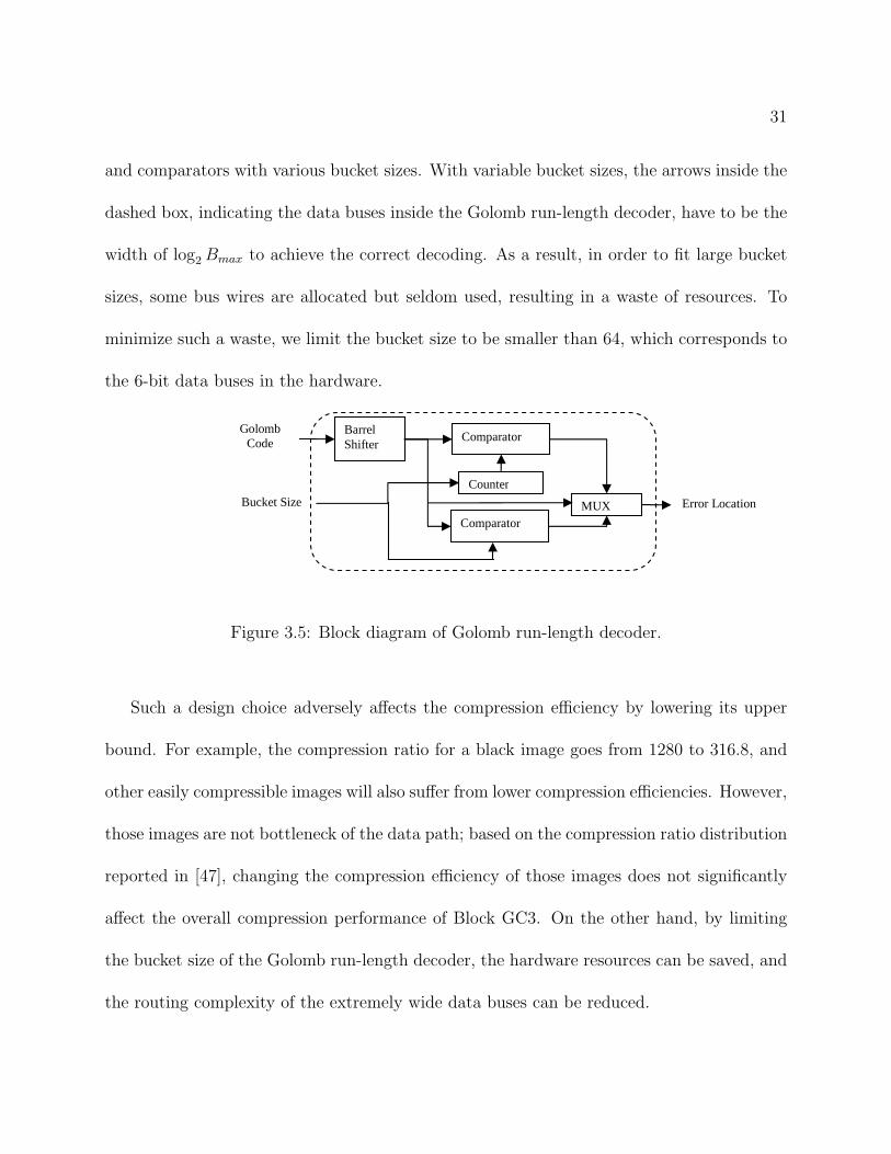
31
and comparators with various bucket sizes. With variable bucket sizes, the arrows inside the
dashed box, indicating the data buses inside the Golomb run-length decoder, have to be the
width of log2 Bmax to achieve the correct decoding. As a result, in order to fit large bucket
sizes, some bus wires are allocated but seldom used, resulting in a waste of resources. To
minimize such a waste, we limit the bucket size to be smaller than 64, which corresponds to
the 6-bit data buses in the hardware.
Barrel Shifter
Counter
Comparator
Comparator MUX
Golomb Code
Bucket Size Error Location
Figure 3.5: Block diagram of Golomb run-length decoder.
Such a design choice adversely affects the compression efficiency by lowering its upper
bound. For example, the compression ratio for a black image goes from 1280 to 316.8, and
other easily compressible images will also suffer from lower compression efficiencies. However,
those images are not bottleneck of the data path; based on the compression ratio distribution
reported in [47], changing the compression efficiency of those images does not significantly
affect the overall compression performance of Block GC3. On the other hand, by limiting
the bucket size of the Golomb run-length decoder, the hardware resources can be saved, and
the routing complexity of the extremely wide data buses can be reduced.
32
3.4 Fixed Codeword for Huffman Decoder
Similar to other entropy codes, Huffman code adapts its codeword according to the
statistics of the input data stream to achieve the highest compression efficiency. In general,
the codeword is either derived from the input data itself, or by the training data with the
same statistics. In both scenarios, the code table in the Huffman decoder has to be updated
to reflect the statistical change of the input data stream. For layout images, this corresponds
to either different layers or different parts of the layout. However, the updating of the code
table requires an additional data stream to be transmitted from encoder to the decoder.
Moreover, the update of the code table has to be done in the background such that the
current decoding is not affected. Consequently, more internal buffers are introduced, and
additional data is transmitted over the data path.
Close examination of the statistics of input data stream, namely, the image error val-
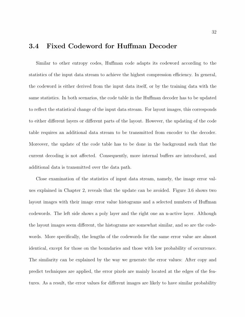
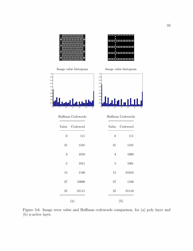
ues explained in Chapter 2, reveals that the update can be avoided. Figure 3.6 shows two
layout images with their image error value histograms and a selected numbers of Huffman
codewords. The left side shows a poly layer and the right one an n-active layer. Although
the layout images seem different, the histograms are somewhat similar, and so are the code-
words. More specifically, the lengths of the codewords for the same error value are almost
identical, except for those on the boundaries and those with low probability of occurrence.
The similarity can be explained by the way we generate the error values: After copy and
predict techniques are applied, the error pixels are mainly located at the edges of the fea-
tures. As a result, the error values for different images are likely to have similar probability
33
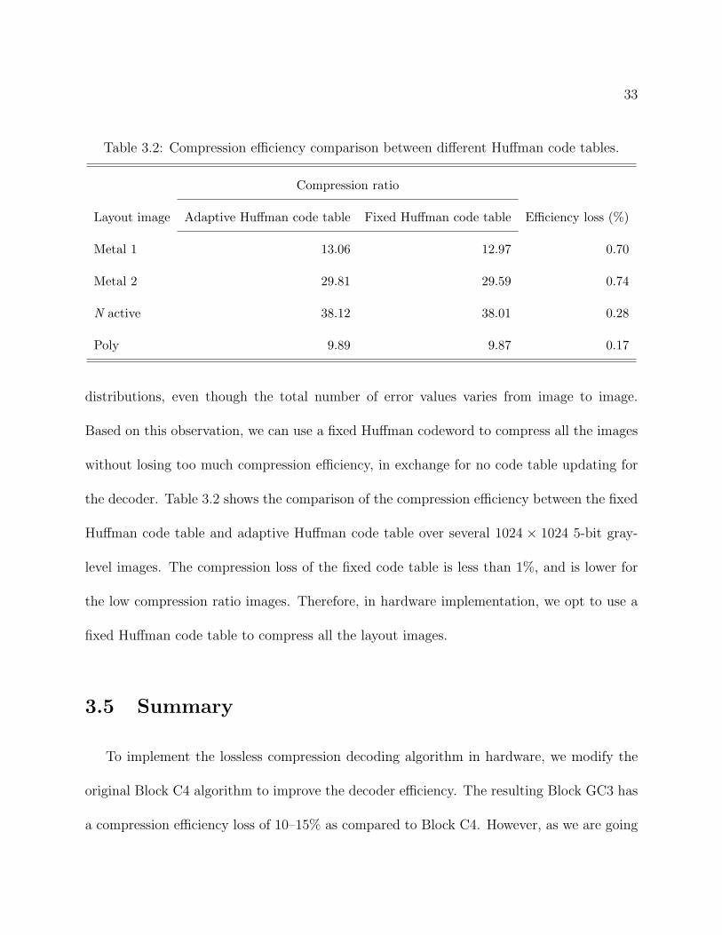
Table 3.2: Compression efficiency comparison between different Huffman code tables.
Compression ratio
Layout image Adaptive Huffman code table Fixed Huffman code table Efficiency loss (%)
Metal 1 13.06 12.97 0.70
Metal 2 29.81 29.59 0.74
N active 38.12 38.01 0.28
Poly 9.89 9.87 0.17
distributions, even though the total number of error values varies from image to image.
Based on this observation, we can use a fixed Huffman codeword to compress all the images
without losing too much compression efficiency, in exchange for no code table updating for
the decoder. Table 3.2 shows the comparison of the compression efficiency between the fixed
Huffman code table and adaptive Huffman code table over several 1024 × 1024 5-bit gray-
level images. The compression loss of the fixed code table is less than 1%, and is lower for
the low compression ratio images. Therefore, in hardware implementation, we opt to use a
fixed Huffman code table to compress all the layout images.
3.5 Summary
To implement the lossless compression decoding algorithm in hardware, we modify the
original Block C4 algorithm to improve the decoder efficiency. The resulting Block GC3 has
a compression efficiency loss of 10–15% as compared to Block C4. However, as we are going
34
Image value histogram Image value histogram
0 5 10 15 20 25 300
0.02
0.04
0.06
0.08
0.1
0.12
0.14
0.16
0.18
0.2
0 5 10 15 20 25 300
0.02
0.04
0.06
0.08
0.1
0.12
0.14
0.16
0.18
0.2
Huffman Codewords Huffman Codewords
Value Codeword
0 111
31 1101
3 1010
5 1011
15 1100
27 10000
25 01111
Value Codeword
0 111
31 1101
3 1000
5 1001
15 01010
27 1100
25 01110
(a) (b)
Figure 3.6: Image error value and Huffman codewords comparison, for (a) poly layer and(b) n-active layer.
35
to show in the next chapter, the decoder design of Block GC3 is much simpler than that of
Block C4, thus compensating the compression efficiency loss.
In addition, we restrain the parameter selection for Block GC3, such as defining the
maximum bucket size for Golomb run-length code, and using a fixed Huffman code table for
image error value coding. As a result, the data bus in the decoder is utilized more, and the
input data transmission overhead is reduced.
With these modifications, the lossless decompression algorithm is ready to be imple-
mented in hardware. In the next chapter, we are going to decribe the implementation in
detail.
36
Chapter 4
Hardware Design of Block C4 and
Block GC3 Decoders
4.1 Introduction
For the decoder to be used in a maskless lithography data path, it must be implemented
as a custom-designed digital circuit and included on the same chip with the writer array.
In addition, to achieve a system with high level of parallelism, the decoder must have data-
flow architecture and high throughput. By analyzing the functional blocks of the Block C4
and Block GC3 algorithms, we devise the data-flow architecture for the decoder. The block
diagram of Block C4 decoder is shown in Figure 4.1. There are three main inputs: the seg-
mentation, the compressed error location, and the compressed error value. The segmentation
is fed into the Region Decoder, generating a segmentation map as needed by the decoding
37
process. Using this map, the decoded predict/copy property of each pixel can be used to
select between the predicted value from Linear Prediction and the copied value from History
Buffer in the Control/Merge stage, as shown in Figure 4.2. The compressed pixel error loca-
tion is decoded by HCC, resulting in an error location map, which indicates the locations of
invalid predict/copy pixels. In the decoder, this map contributes to another control signal
in the Control/Merge stage to select the final output pixel value from either predict/copy
value or the decompressed error value generated by Huffman decoder. The output data is
written back to History Buffer for future usage, either for linear prediction or for copying,
where the appropriate access position in the buffer is generated by Address Generator. All
the decoding operations are combinations of basic logic and arithmetic operations, such as
selection, addition, and subtraction. By applying the tradeoffs described in Chapter 3, the
total amount of needed memory inside a single Block C4 decoder is about 1.7 KB, which
can be implemented using on-chip SRAM.
History Buffer
Region Decoder
Address Generator
Linear Prediction
l/a, d
Control/ Merge
Huffman Decoder
HCC Decoder
predict/copy
error location
error value
copy value
predict value
address
Writer
Segmentation
Compressed
Error Value
Compressed
Error Location
Figure 4.1: Functional block diagram of the decoder.
38
mux
pixel value from
Linear Prediction
mux
pixel value from
Huffman
predict/copy error location
pixel value from
History Buffer
Figure 4.2: The block diagram of Merge/Control block.
The block diagram of Block GC3 is almost identical to that of Block C4 shown in Fig-
ure 4.1, since it only replaces the HCC block of Block C4 by a Golomb run-length decoder.
In the remainder of this chapter, we discuss the architecture for the Block C4 and Block
GC3 decoders. We will break down all seven major blocks and describe the function in
detail. The Simulink schematics of the blocks will be shown in Appendix B. We also present
the FPGA and ASIC implementation and synthesis results of Block GC3 decoder.
4.2 Block C4
In this section, we examine the functional blocks inside Block C4 decoder and discuss
the implementation and the cost of each block.
4.2.1 Linear Predictor
For flattened, rasterized layout images, in order to correctly preserve horizontal and verti-
cal edges, we use a 3-pixel linear prediction model to predict the 5-bit gray level images. The
prediction strategy is similar to the binary image context-based prediction in [14]. However,
39
in this block, we only use arithmetic operations instead of table look-up to predict the image
pixel values. Besides the 3-pixel based linear prediction, this block also sets two thresholds
of 0 and 31 to detect the overflow from addition and subtraction. The block diagram is
shown in Figure 4.3.
Reg.
Counter
=
0
0
0
+
31
0
0
0
1
1
1
1
5
5
5
5
5
0
05
+
-
<=0 >=31
Input b
Input c
Output
5
5 5
10
Figure 4.3: The block diagram of Linear Predictor.
a b
c z
x = b – a + cif (x < 0) then z = 0 if (x > max) then z = max
otherwise z = x
Figure 4.4: The algorithm of 3-pixel based linear prediction.
The 3-pixel based linear prediction algorithm is shown in Figure 4.4. Pixel z is the
current pixel we are predicting, and a, b, and c are three adjacent pixels on the upper, left,
and upper-left corner; by applying this simple linear prediction, the horizontal and vertical
40
edges of the layout images can be preserved, as discussed in Chapter 2. In terms of the
implementation of the predictor, we merely have two inputs: pixel b from the history buffer,
and pixel c the system output from the previous cycle; pixel a is the delayed version of b. In
addition, we set the upper and left boundaries to 0 in order to provide the initial condition
of the linear prediction. Although there are both addition and substraction in the block,
we do not have to use two’s compliment data representation; since the pixel values are all
positive, it is not necessary to spend one extra sign bit to represent the negative values. All
we have to do is to check the carry-out output of both adder and subtractor to make sure
we handle the overflow cases properly.
4.2.2 Region Decoder
Architecture
In the C4 algorithm, each flattened, rasterized layout image is divided into copy and
predict regions; copy distances and directions for copy regions are also annotated so that
the decoder can access the history buffer properly. Similar to an actual IC layout, the
segmentation map is also Manhattan shaped, and can be compressed by the prediction al-
gorithm. However, since the segmentation map, consisting of the segmentation information
(predict/copy, direction, distance), is an artificial image, there is no correlation between the
information of adjacent regions. Considering the simplicity and the benefit from several
prediction algorithms, the segmentation predictor shown in Figure 4.5 is used in the region
decoder rather than the linear predictor used for pixel predictions in a layout. The resulting
41
two bit streams, the segmentation error location and the segmentation error value, are trans-
mitted to the decoder. In particular, the segmentation error location is further compressed
using Golomb run-length code.
a b
c z
If (c = a) then z = b
else z = c
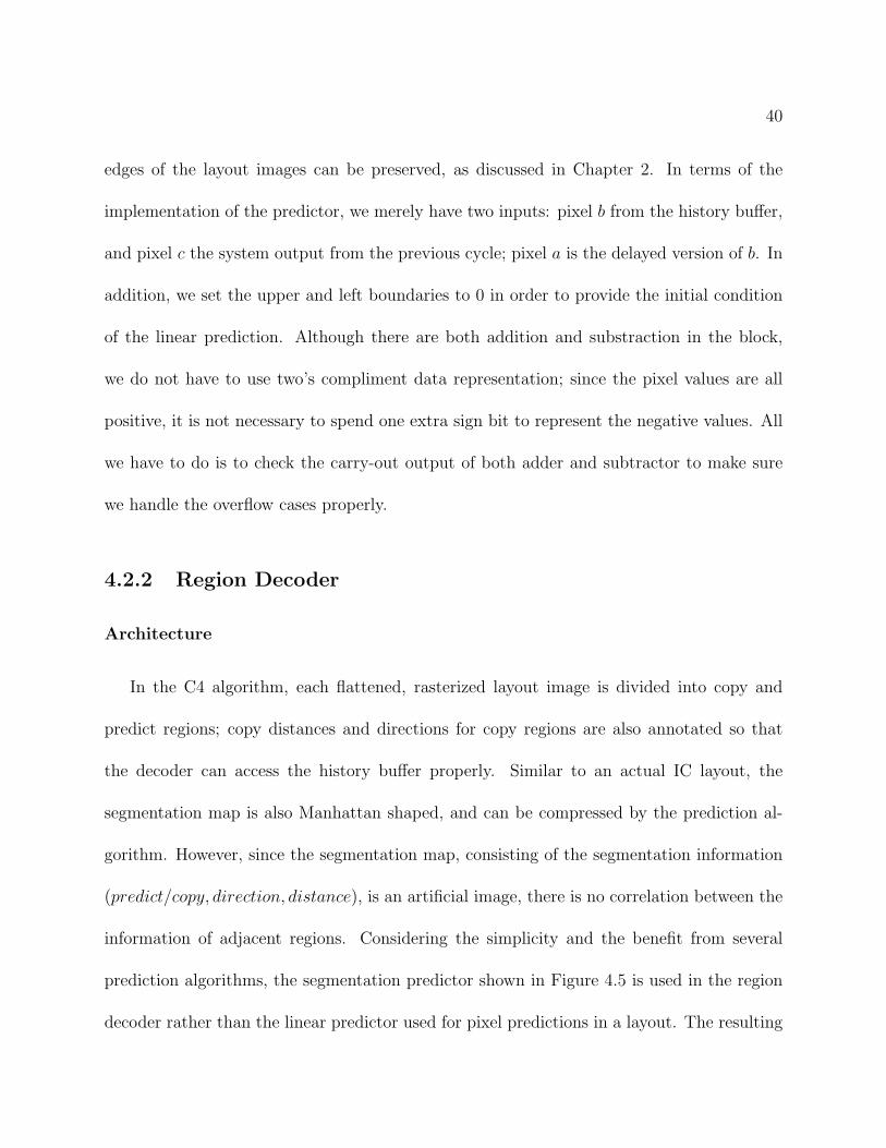
Figure 4.5: The context prediction algorithm for the segmentation information.
In the decoder, the region decoder block restores the segmentation information for each
8 × 8 image microblock from the compressed segmentation error location and the segmen-
tation error value. Furthermore, it has to convert the segmentation information from the
8× 8 block domain to the pixel domain, since the other operations in the decoder are done
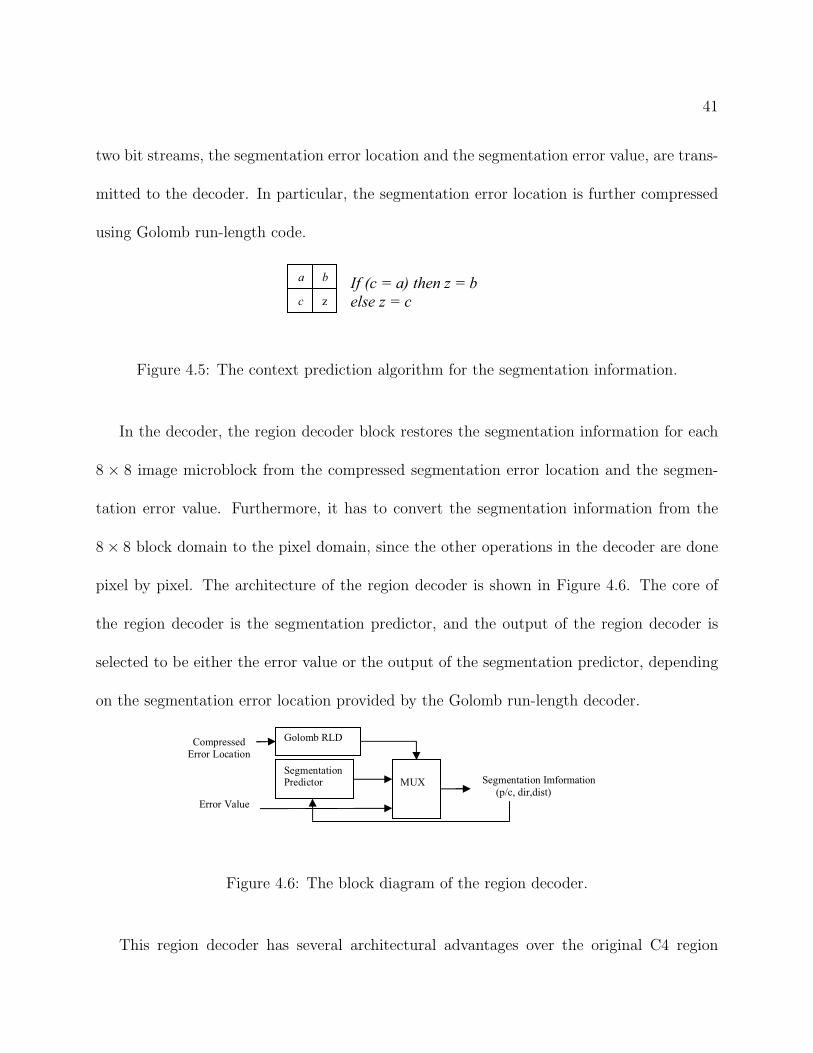
pixel by pixel. The architecture of the region decoder is shown in Figure 4.6. The core of
the region decoder is the segmentation predictor, and the output of the region decoder is
selected to be either the error value or the output of the segmentation predictor, depending
on the segmentation error location provided by the Golomb run-length decoder.
Golomb RLD
Segmentation Predictor MUX
Compressed
Error Location
Error Value
Segmentation Imformation
(p/c, dir,dist)
Figure 4.6: The block diagram of the region decoder.
This region decoder has several architectural advantages over the original C4 region
42
decoder [10]. First, it is implemented as a regular data path, in contrast to a linked-list
structure, thus eliminating feedback and latency issues. Second, the output of the Block C4
region decoder is the control signal over an 8 × 8 microblock, which lowers the output rate
of the region decoder by 64, and reduces the power consumption. Finally, the length of the
input of the region decoder is reduced from 51 bits (x, y, w, ℎ, dir, dist) to 13 bits, i.e., 1-bit
error location and 12-bit error value, and can be further packaged, resulting in fewer I/O
pins in the decoder.
Segmentation Predictor
As we stated previously, the segmentation predictor is the core of the region decoder. Its
implementation is very similar to the linear predictor block with two exceptions: there is
no microblock inputs for segmentation prediction, and the output has to be converted from
the 8× 8 microblock domain to the pixel domain in the rasterized, i.e., left to right, top to
bottom.
Figure 4.7 shows the schematics of the segmentation predictor. Note microblocks a, b,
and c of Figure 4.5 are now implemented as part of the delay chain of the output, resulting in
a self-contained predictor. The output of the predictor may be replaced by the segmentation
error value depending on the segmentation error location.
To convert the segmentation information to the pixel domain, we apply two delay blocks,
each 1024/8 = 128 words long, in the predictor to relay the segmentation information within
an 8× 8 block of pixels. As shown in Figure 4.7, the first delay block is used to keep track
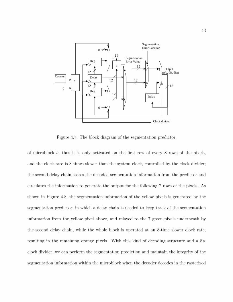
43
Delay
Reg.
Reg.
Counter
=
0
0
0
=
Segmentation Error Location
Segmentation Error Value 0
0
0
1
1
1
1
12
12
12
12
12
12
12
12
0
0
1 Output (p/c, dir, dist)
Delay
Clock divider
Figure 4.7: The block diagram of the segmentation predictor.
of microblock b; thus it is only activated on the first row of every 8 rows of the pixels,
and the clock rate is 8 times slower than the system clock, controlled by the clock divider;
the second delay chain stores the decoded segmentation information from the predictor and
circulates the information to generate the output for the following 7 rows of the pixels. As
shown in Figure 4.8, the segmentation information of the yellow pixels is generated by the
segmentation predictor, in which a delay chain is needed to keep track of the segmentation
information from the yellow pixel above, and relayed to the 7 green pixels underneath by
the second delay chain, while the whole block is operated at an 8-time slower clock rate,
resulting in the remaining orange pixels. With this kind of decoding structure and a 8×
clock divider, we can perform the segmentation prediction and maintain the integrity of the
segmentation information within the microblock when the decoder decodes in the rasterized
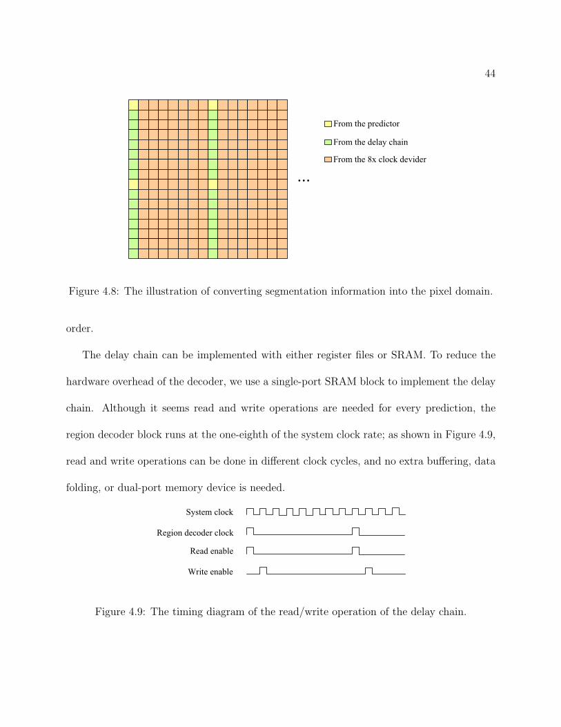
44
From the predictor
...
From the delay chain
From the 8x clock devider
Figure 4.8: The illustration of converting segmentation information into the pixel domain.
order.
The delay chain can be implemented with either register files or SRAM. To reduce the
hardware overhead of the decoder, we use a single-port SRAM block to implement the delay
chain. Although it seems read and write operations are needed for every prediction, the
region decoder block runs at the one-eighth of the system clock rate; as shown in Figure 4.9,
read and write operations can be done in different clock cycles, and no extra buffering, data
folding, or dual-port memory device is needed.
System clock
Region decoder clock
Read enable
Write enable
Figure 4.9: The timing diagram of the read/write operation of the delay chain.
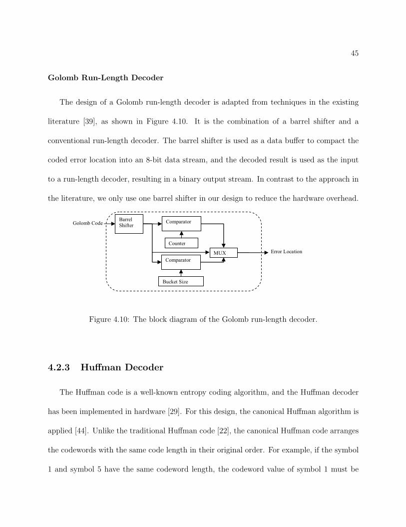
45
Golomb Run-Length Decoder
The design of a Golomb run-length decoder is adapted from techniques in the existing
literature [39], as shown in Figure 4.10. It is the combination of a barrel shifter and a
conventional run-length decoder. The barrel shifter is used as a data buffer to compact the
coded error location into an 8-bit data stream, and the decoded result is used as the input
to a run-length decoder, resulting in a binary output stream. In contrast to the approach in
the literature, we only use one barrel shifter in our design to reduce the hardware overhead.
Barrel Shifter
Counter
Comparator
Comparator
Bucket Size
MUX
Golomb Code
Error Location
Figure 4.10: The block diagram of the Golomb run-length decoder.
4.2.3 Huffman Decoder
The Huffman code is a well-known entropy coding algorithm, and the Huffman decoder
has been implemented in hardware [29]. For this design, the canonical Huffman algorithm is
applied [44]. Unlike the traditional Huffman code [22], the canonical Huffman code arranges
the codewords with the same code length in their original order. For example, if the symbol
1 and symbol 5 have the same codeword length, the codeword value of symbol 1 must be
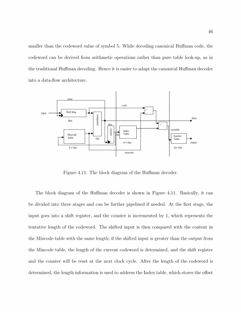
46
smaller than the codeword value of symbol 5. While decoding canonical Huffman code, the
codeword can be derived from arithmetic operations rather than pure table look-up, as in
the traditional Huffman decoding. Hence it is easier to adapt the canonical Huffman decoder
into a data-flow architecture.
Shift Reg.
Mincode Table
com
pa
rator cou
nter
Index Table
+
+
Symbol Table
-
len
reset
input
mincode
code
symaddr
output
done
8 × 5bit
8 × 5bit
8bit
32× 5bit
5bit
5bit
Figure 4.11: The block diagram of the Huffman decoder.
The block diagram of the Huffman decoder is shown in Figure 4.11. Basically, it can
be divided into three stages and can be further pipelined if needed. At the first stage, the
input goes into a shift register, and the counter is incremented by 1, which represents the
tentative length of the codeword. The shifted input is then compared with the content in
the Mincode table with the same length; if the shifted input is greater than the output from
the Mincode table, the length of the current codeword is determined, and the shift register
and the counter will be reset at the next clock cycle. After the length of the codeword is
determined, the length information is used to address the Index table, which stores the offset
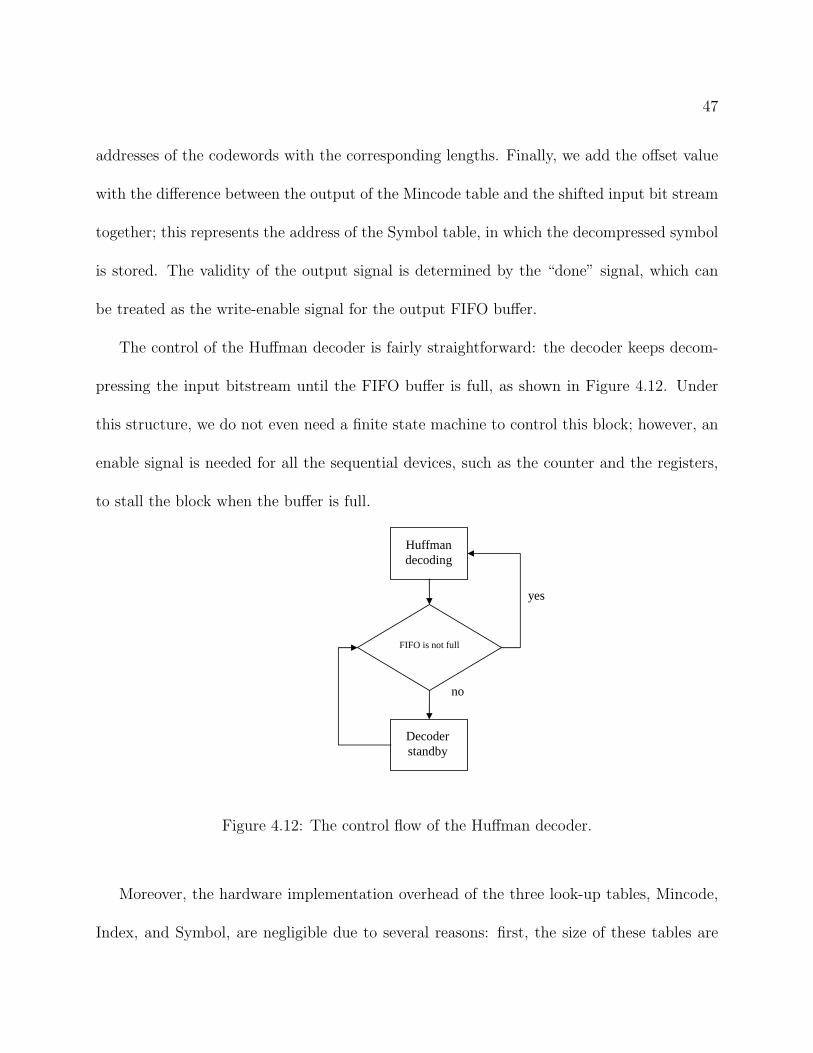
47
addresses of the codewords with the corresponding lengths. Finally, we add the offset value
with the difference between the output of the Mincode table and the shifted input bit stream
together; this represents the address of the Symbol table, in which the decompressed symbol
is stored. The validity of the output signal is determined by the “done” signal, which can
be treated as the write-enable signal for the output FIFO buffer.
The control of the Huffman decoder is fairly straightforward: the decoder keeps decom-
pressing the input bitstream until the FIFO buffer is full, as shown in Figure 4.12. Under
this structure, we do not even need a finite state machine to control this block; however, an
enable signal is needed for all the sequential devices, such as the counter and the registers,
to stall the block when the buffer is full.
FIFO is not full
Huffman decoding
Decoder standby
no
yes
Figure 4.12: The control flow of the Huffman decoder.
Moreover, the hardware implementation overhead of the three look-up tables, Mincode,
Index, and Symbol, are negligible due to several reasons: first, the size of these tables are
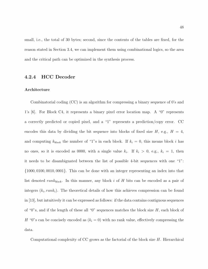
48
small, i.e., the total of 30 bytes; second, since the contents of the tables are fixed, for the
reason stated in Section 3.4, we can implement them using combinational logics, so the area
and the critical path can be optimized in the synthesis process.
4.2.4 HCC Decoder
Architecture
Combinatorial coding (CC) is an algorithm for compressing a binary sequence of 0’s and
1’s [6]. For Block C4, it represents a binary pixel error location map. A “0” represents
a correctly predicted or copied pixel, and a “1” represents a prediction/copy error. CC
encodes this data by dividing the bit sequence into blocks of fixed size H, e.g., H = 4,
and computing kblock the number of “1”s in each block. If ki = 0, this means block i has
no ones, so it is encoded as 0000, with a single value ki. If ki > 0, e.g., ki = 1, then
it needs to be disambiguated between the list of possible 4-bit sequences with one “1”:
{1000, 0100, 0010, 0001}. This can be done with an integer representing an index into that
list denoted rankblock. In this manner, any block i of H bits can be encoded as a pair of
integers (ki, ranki). The theoretical details of how this achieves compression can be found
in [13], but intuitively it can be expressed as follows: if the data contains contiguous sequences
of “0”s, and if the length of these all “0” sequences matches the block size H, each block of
H “0”s can be concisely encoded as (ki = 0) with no rank value, effectively compressing the
data.
Computational complexity of CC grows as the factorial of the block size H. Hierarchical
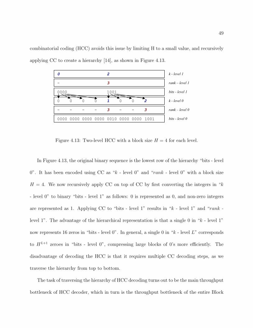
49
combinatorial coding (HCC) avoids this issue by limiting H to a small value, and recursively
applying CC to create a hierarchy [14], as shown in Figure 4.13.
0000 0000 0000 0000 0010 0000 0000 1001
0 0 0 0 1 0 0 2
0000 1001
0 2
bits - level 0
k - level 0
bits - level 1
k - level 1
- 3 rank – level 1
- - - - 3 - - 3 rank – level 0
Figure 4.13: Two-level HCC with a block size H = 4 for each level.
In Figure 4.13, the original binary sequence is the lowest row of the hierarchy “bits - level
0”. It has been encoded using CC as “k - level 0” and “rank - level 0” with a block size
H = 4. We now recursively apply CC on top of CC by first converting the integers in “k
- level 0” to binary “bits - level 1” as follows: 0 is represented as 0, and non-zero integers
are represented as 1. Applying CC to “bits - level 1” results in “k - level 1” and “rank -
level 1”. The advantage of the hierarchical representation is that a single 0 in “k - level 1”
now represents 16 zeros in “bits - level 0”. In general, a single 0 in “k - level L” corresponds
to HL+1 zeroes in “bits - level 0”, compressing large blocks of 0’s more efficiently. The
disadvantage of decoding the HCC is that it requires multiple CC decoding steps, as we
traverse the hierarchy from top to bottom.
The task of traversing the hierarchy of HCC decoding turns out to be the main throughput
bottleneck of HCC decoder, which in turn is the throughput bottleneck of the entire Block
50
C4 decoder. The block diagram of a sequential HCC decoder is shown in Figure 4.14(a).
Block C4 uses a 3-level H = 8 HCC decoder. The dashed lines separate the HCC levels from
top to bottom, and the data that moves between levels are the bits - level L. Three CC
blocks represent (k, rank) decoders for levels 2, 1, and 0, from top to bottom respectively.
CC - level 2 decodes to bits - level 2. If bits - level 2 is a “0” bit, the MUX selects the
run-length decoder (RLD) block which generates 8 zeros for bits - level 1. Otherwise, the
MUX selects the CC - level 1 block to decode a (k, rank) pair. Likewise, bits, level - 1
controls the MUX in level 0. A “0” causes the RLD block to generate 8 zeros, and a “1”
causes CC - level 0 to decode a (k, rank) pair. In this sequential design, the output of a
lower level must wait for the output of a higher level to be available before it can continue.
Consequently, the control signal corresponding to when the output of the lowest level bits
level - 0 is ready resembles Figure 4.14(c). While levels 2 and 1 are decoding as indicated by
the shaded boxes, the output of layer 0 must stall, reducing the effective overall throughput
of the HCC block.
To overcome the problem of hierarchical HCC decoding, we can parallelize the operation
by introducing a FIFO buffer between HCC levels, as indicated by the additional squares in
Figure 4.14(b), and by dividing the input (k, rank) values for each HCC level into multiple
sub-streams. The idea is that after an initial delay to fill the buffers of levels 2 and 1, level 0
can decode continuously as long as the buffers are not empty. This is guaranteed because one
level 2 output bit corresponds to 8 level 1 output bits, and 64 level 0 output bits. Level 2 and
level 1 can continue to decode into these buffers while level 0 is operating. Consequently, the
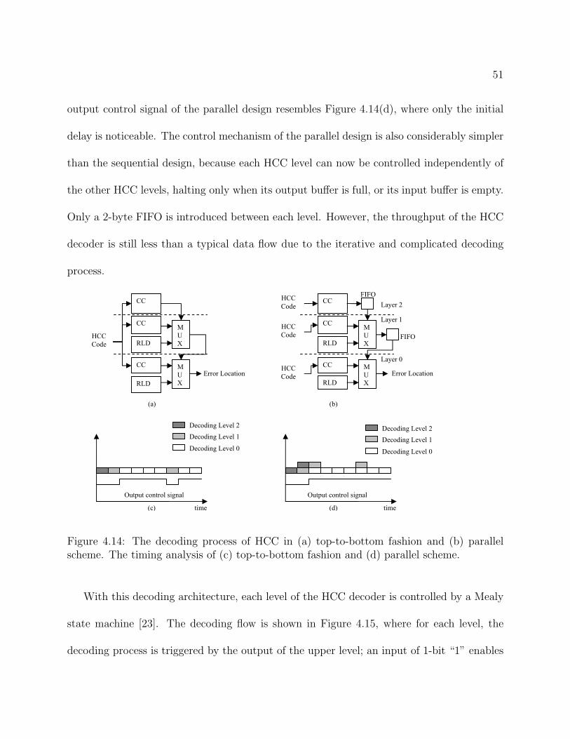
51
output control signal of the parallel design resembles Figure 4.14(d), where only the initial
delay is noticeable. The control mechanism of the parallel design is also considerably simpler
than the sequential design, because each HCC level can now be controlled independently of
the other HCC levels, halting only when its output buffer is full, or its input buffer is empty.
Only a 2-byte FIFO is introduced between each level. However, the throughput of the HCC
decoder is still less than a typical data flow due to the iterative and complicated decoding
process.
CC
CC
RLD
CC
RLD
M
U
X
M
U
X
CC
CC
RLD
CC
RLD
M
U
X
M
U
X
Layer 2
Layer 1
Layer 0
(b) (a)
FIFO
FIFO
Decoding Level 2
Decoding Level 1
Decoding Level 0
(c) (d)
Output control signal Output control signal
time time
Decoding Level 2
Decoding Level 1
Decoding Level 0
HCC
Code HCC
Code
HCC
Code
HCC
Code Error Location Error Location
Figure 4.14: The decoding process of HCC in (a) top-to-bottom fashion and (b) parallelscheme. The timing analysis of (c) top-to-bottom fashion and (d) parallel scheme.
With this decoding architecture, each level of the HCC decoder is controlled by a Mealy
state machine [23]. The decoding flow is shown in Figure 4.15, where for each level, the
decoding process is triggered by the output of the upper level; an input of 1-bit “1” enables
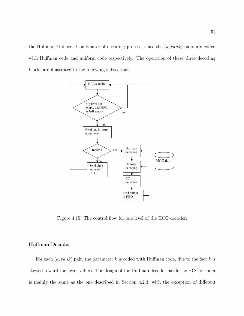
52
the Huffman–Uniform–Combinatorial decoding process, since the (k, rank) pairs are coded
with Huffman code and uniform code respectively. The operation of these three decoding
blocks are illustrated in the following subsections.
HCC standby
Up level not empty and FIFO is half empty
Read one bit from upper level
Input=1 Huffman decoding
Uniform decoding
CC decoding
Send eight zeros to FIFO
Send output to FIFO
HCC data
yes
no
no
yes
Figure 4.15: The control flow for one level of the HCC decoder.
Huffman Decoder
For each (k, rank) pair, the parameter k is coded with Huffman code, due to the fact k is
skewed toward the lower values. The design of the Huffman decoder inside the HCC decoder
is mainly the same as the one described in Section 4.2.3, with the exception of different
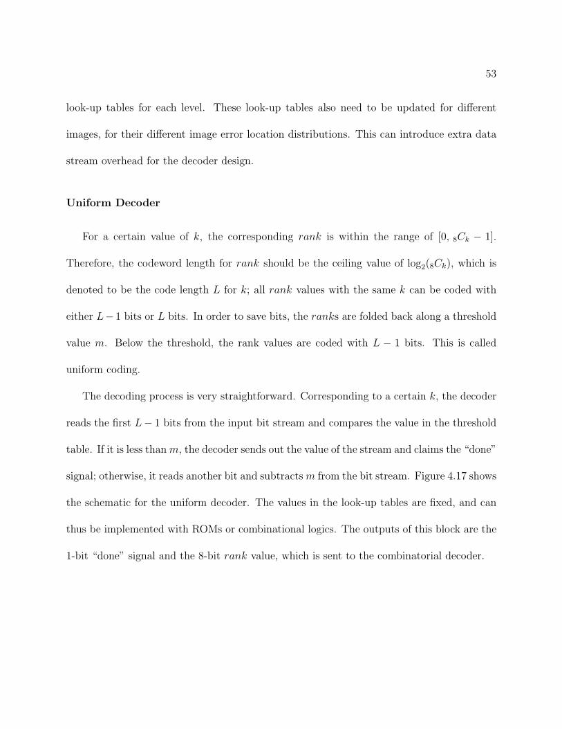
53
look-up tables for each level. These look-up tables also need to be updated for different
images, for their different image error location distributions. This can introduce extra data
stream overhead for the decoder design.
Uniform Decoder
For a certain value of k, the corresponding rank is within the range of [0, 8Ck − 1].
Therefore, the codeword length for rank should be the ceiling value of log2(8Ck), which is
denoted to be the code length L for k; all rank values with the same k can be coded with
either L− 1 bits or L bits. In order to save bits, the ranks are folded back along a threshold
value m. Below the threshold, the rank values are coded with L − 1 bits. This is called
uniform coding.
The decoding process is very straightforward. Corresponding to a certain k, the decoder
reads the first L− 1 bits from the input bit stream and compares the value in the threshold
table. If it is less thanm, the decoder sends out the value of the stream and claims the “done”
signal; otherwise, it reads another bit and subtractsm from the bit stream. Figure 4.17 shows
the schematic for the uniform decoder. The values in the look-up tables are fixed, and can
thus be implemented with ROMs or combinational logics. The outputs of this block are the
1-bit “done” signal and the 8-bit rank value, which is sent to the combinatorial decoder.
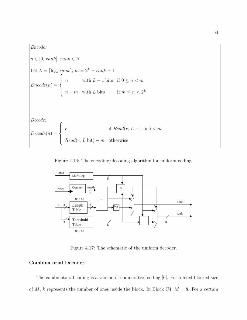
54
Encode:
n ∈ [0, rank], rank ∈ ℕ
Let L = ⌈log2 rank⌉, m = 2L − rank + 1
Encode(n) =
⎧
⎨
⎩
n with L− 1 bits if 0 ≤ n < m
n+m with L bits if m ≤ n < 2L
Decode:
Decode(n) =
⎧
⎨
⎩
r if Read(r, L− 1 bit) < m
Read(r, L bit)−m otherwise
Figure 4.16: The encoding/decoding algorithm for uniform coding.
Shift Reg.
Counter
Threshold Table
Length Table
>=
<
Reg.
+
input
kdone
rank
-
8×3 bit
8×6 bit
0
11
0
lengthreset
86
33
3
3
8
Figure 4.17: The schematic of the uniform decoder.
Combinatorial Decoder
The combinatorial coding is a version of enumerative coding [6]. For a fixed blocked size
of M , k represents the number of ones inside the block. In Block C4, M = 8. For a certain
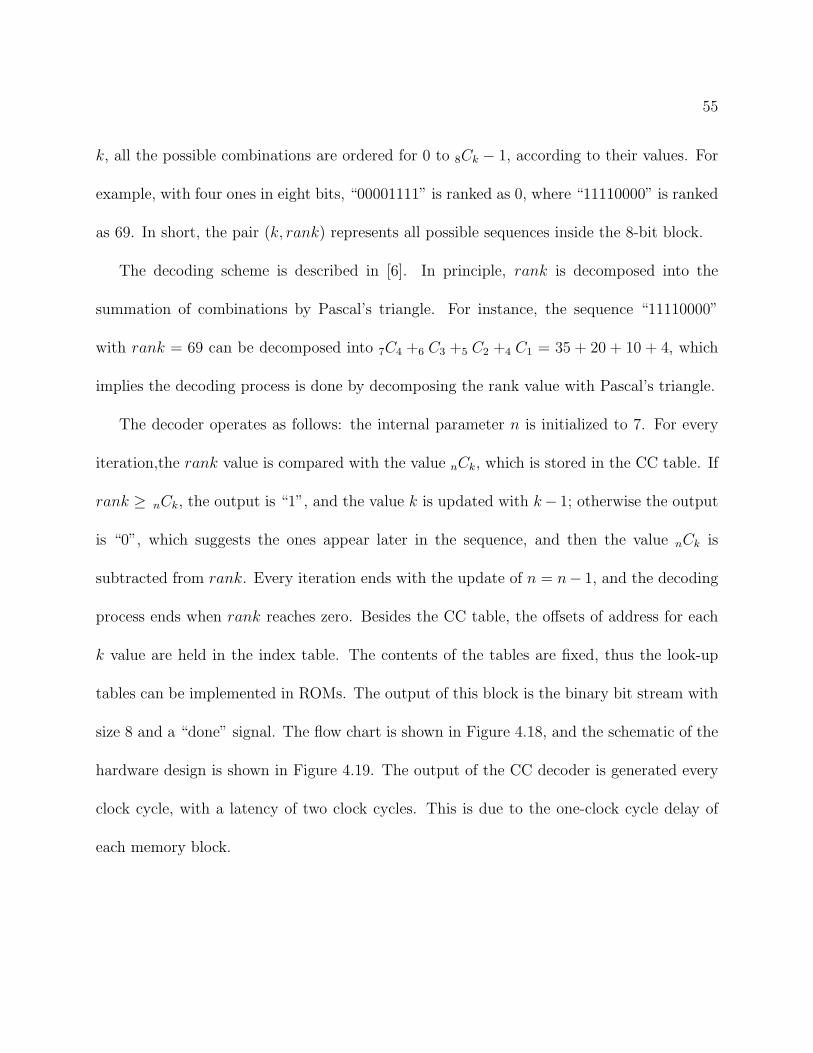
55
k, all the possible combinations are ordered for 0 to 8Ck − 1, according to their values. For
example, with four ones in eight bits, “00001111” is ranked as 0, where “11110000” is ranked
as 69. In short, the pair (k, rank) represents all possible sequences inside the 8-bit block.
The decoding scheme is described in [6]. In principle, rank is decomposed into the
summation of combinations by Pascal’s triangle. For instance, the sequence “11110000”
with rank = 69 can be decomposed into 7C4 +6 C3 +5 C2 +4 C1 = 35 + 20 + 10 + 4, which
implies the decoding process is done by decomposing the rank value with Pascal’s triangle.
The decoder operates as follows: the internal parameter n is initialized to 7. For every
iteration,the rank value is compared with the value nCk, which is stored in the CC table. If
rank ≥ nCk, the output is “1”, and the value k is updated with k− 1; otherwise the output
is “0”, which suggests the ones appear later in the sequence, and then the value nCk is
subtracted from rank. Every iteration ends with the update of n = n− 1, and the decoding
process ends when rank reaches zero. Besides the CC table, the offsets of address for each
k value are held in the index table. The contents of the tables are fixed, thus the look-up
tables can be implemented in ROMs. The output of this block is the binary bit stream with
size 8 and a “done” signal. The flow chart is shown in Figure 4.18, and the schematic of the
hardware design is shown in Figure 4.19. The output of the CC decoder is generated every
clock cycle, with a latency of two clock cycles. This is due to the one-clock cycle delay of
each memory block.
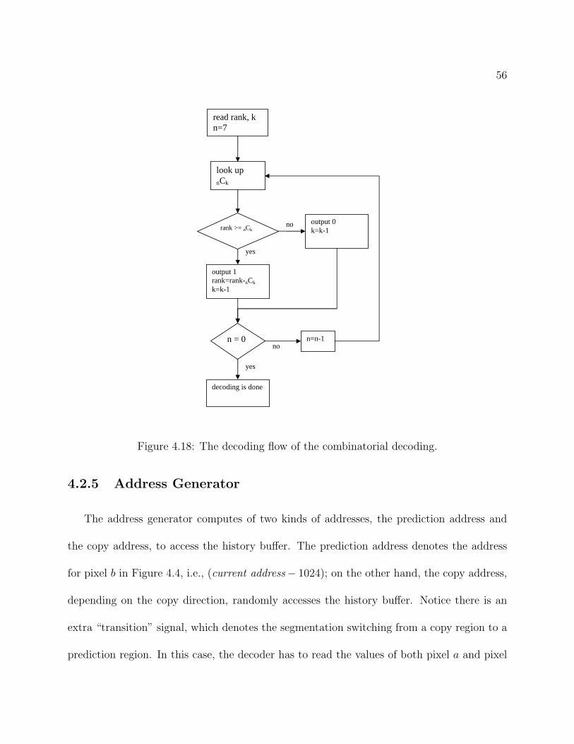
56
read rank, k n=7
look up nCk
rank >= nCk
output 1 rank=rank-nCk
k=k-1
output 0 k=k-1
n = 0
decoding is done
n=n-1
yes
yes
no
no
Figure 4.18: The decoding flow of the combinatorial decoding.
4.2.5 Address Generator
The address generator computes of two kinds of addresses, the prediction address and
the copy address, to access the history buffer. The prediction address denotes the address
for pixel b in Figure 4.4, i.e., (current address− 1024); on the other hand, the copy address,
depending on the copy direction, randomly accesses the history buffer. Notice there is an
extra “transition” signal, which denotes the segmentation switching from a copy region to a
prediction region. In this case, the decoder has to read the values of both pixel a and pixel
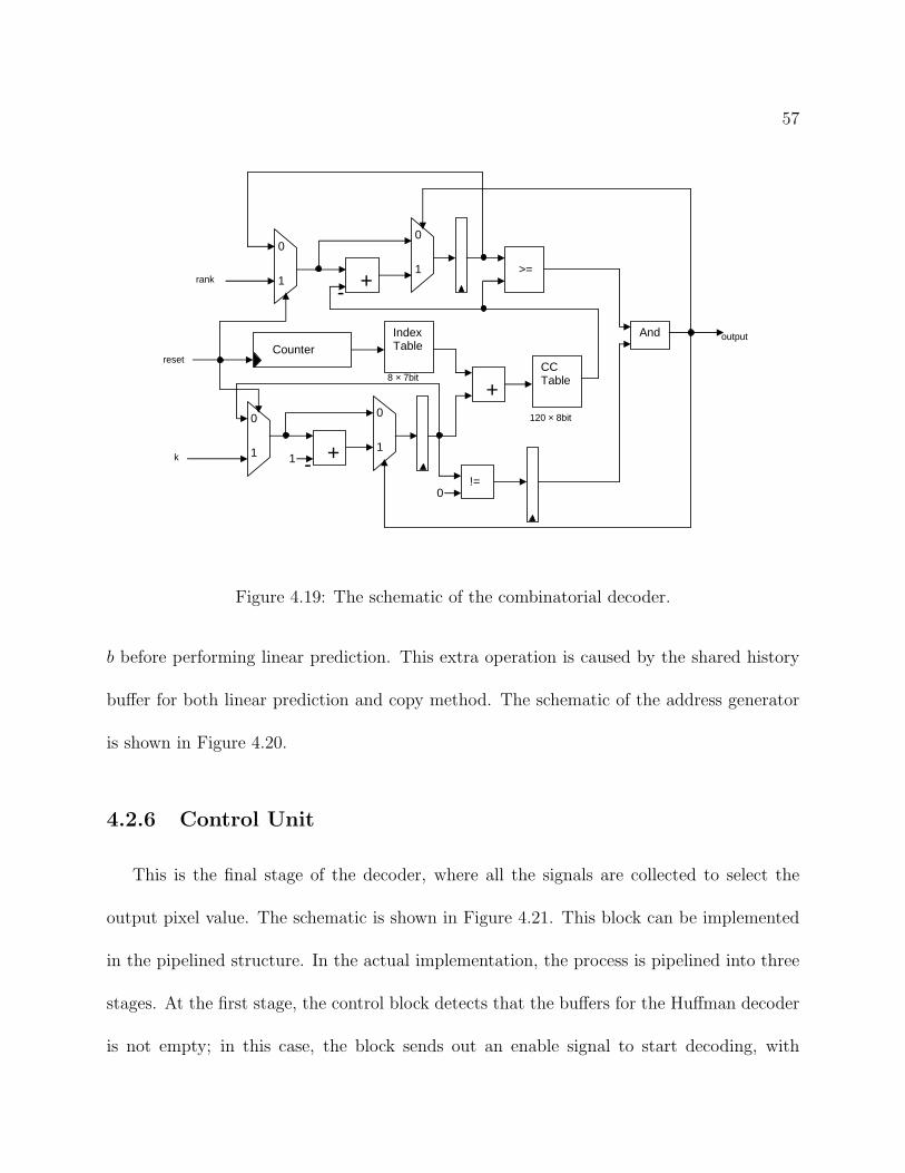
57
Counter
+-
+-
IndexTable
+
!=
CC Table
0
1
0
1
0
1
0
1
0
1
And
>= rank
reset
k
output
120 × 8bit
8 × 7bit
Figure 4.19: The schematic of the combinatorial decoder.
b before performing linear prediction. This extra operation is caused by the shared history
buffer for both linear prediction and copy method. The schematic of the address generator
is shown in Figure 4.20.
4.2.6 Control Unit
This is the final stage of the decoder, where all the signals are collected to select the
output pixel value. The schematic is shown in Figure 4.21. This block can be implemented
in the pipelined structure. In the actual implementation, the process is pipelined into three
stages. At the first stage, the control block detects that the buffers for the Huffman decoder
is not empty; in this case, the block sends out an enable signal to start decoding, with
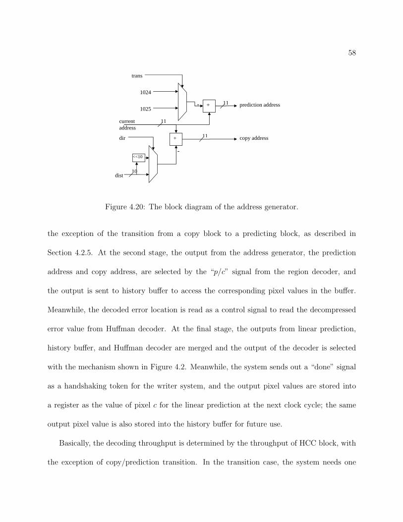
58
+
-<<10
+ -
current address
dist
dir
trans
1024
1025 prediction address
copy address
11
11
11
10
Figure 4.20: The block diagram of the address generator.
the exception of the transition from a copy block to a predicting block, as described in
Section 4.2.5. At the second stage, the output from the address generator, the prediction
address and copy address, are selected by the “p/c” signal from the region decoder, and
the output is sent to history buffer to access the corresponding pixel values in the buffer.
Meanwhile, the decoded error location is read as a control signal to read the decompressed
error value from Huffman decoder. At the final stage, the outputs from linear prediction,
history buffer, and Huffman decoder are merged and the output of the decoder is selected
with the mechanism shown in Figure 4.2. Meanwhile, the system sends out a “done” signal
as a handshaking token for the writer system, and the output pixel values are stored into
a register as the value of pixel c for the linear prediction at the next clock cycle; the same
output pixel value is also stored into the history buffer for future use.
Basically, the decoding throughput is determined by the throughput of HCC block, with
the exception of copy/prediction transition. In the transition case, the system needs one
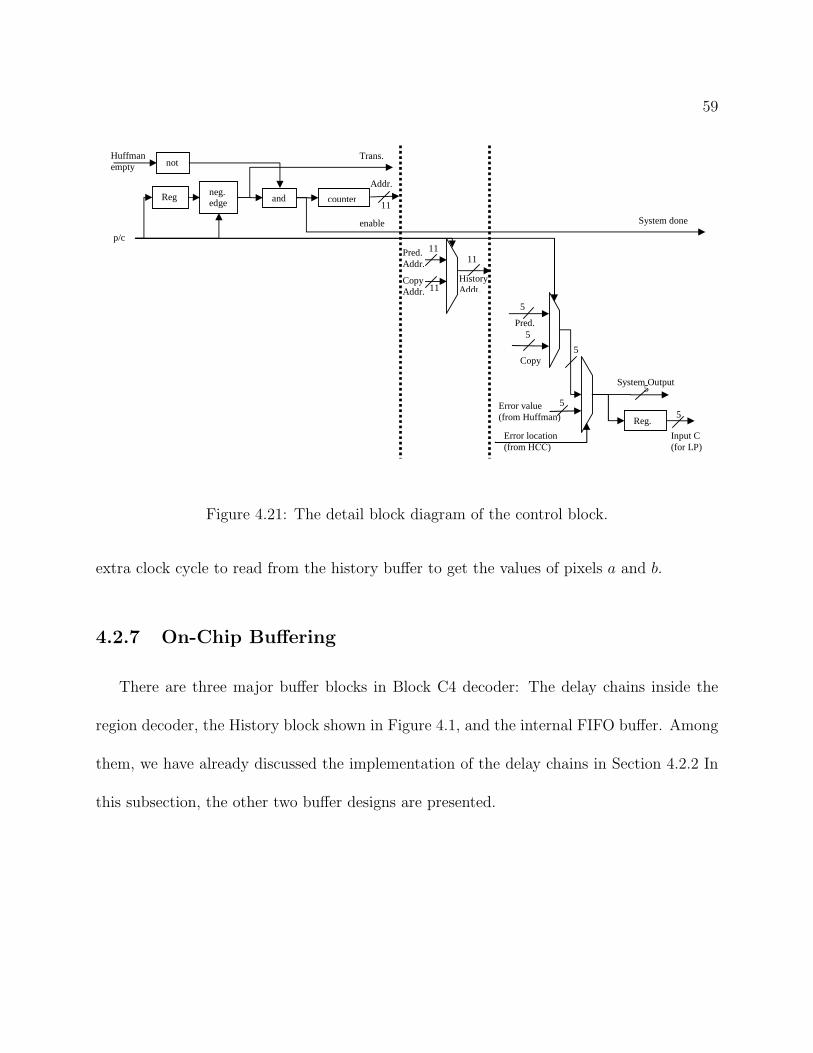
59
not
counterandneg. edge
Reg.
Huffman empty
p/c
Pred. Addr.
Copy Addr.
Addr.
enable
History Addr.
11
11 11
11
Reg.
Pred.
Copy
Error value (from Huffman)
Error location (from HCC)
System Output
Input C (for LP)
5
5
5
5
5
5
Trans.
System done
Figure 4.21: The detail block diagram of the control block.
extra clock cycle to read from the history buffer to get the values of pixels a and b.
4.2.7 On-Chip Buffering
There are three major buffer blocks in Block C4 decoder: The delay chains inside the
region decoder, the History block shown in Figure 4.1, and the internal FIFO buffer. Among
them, we have already discussed the implementation of the delay chains in Section 4.2.2 In
this subsection, the other two buffer designs are presented.
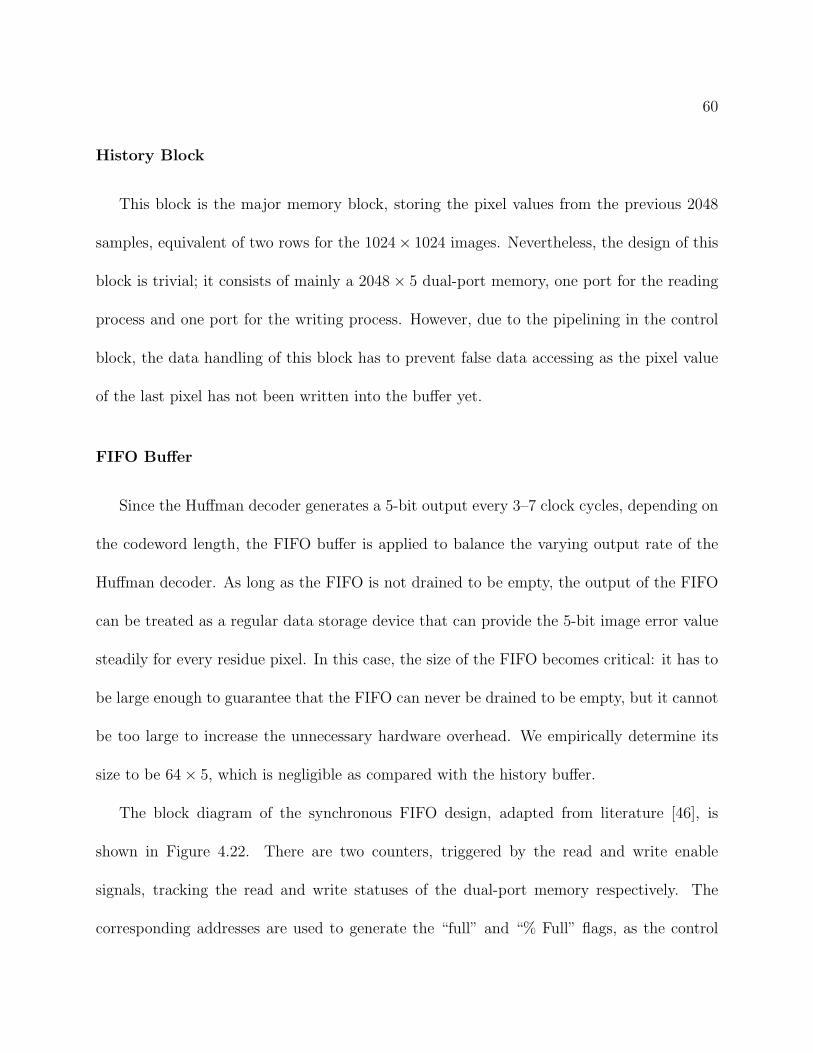
60
History Block
This block is the major memory block, storing the pixel values from the previous 2048
samples, equivalent of two rows for the 1024× 1024 images. Nevertheless, the design of this
block is trivial; it consists of mainly a 2048× 5 dual-port memory, one port for the reading
process and one port for the writing process. However, due to the pipelining in the control
block, the data handling of this block has to prevent false data accessing as the pixel value
of the last pixel has not been written into the buffer yet.
FIFO Buffer
Since the Huffman decoder generates a 5-bit output every 3–7 clock cycles, depending on
the codeword length, the FIFO buffer is applied to balance the varying output rate of the
Huffman decoder. As long as the FIFO is not drained to be empty, the output of the FIFO
can be treated as a regular data storage device that can provide the 5-bit image error value
steadily for every residue pixel. In this case, the size of the FIFO becomes critical: it has to
be large enough to guarantee that the FIFO can never be drained to be empty, but it cannot
be too large to increase the unnecessary hardware overhead. We empirically determine its
size to be 64× 5, which is negligible as compared with the history buffer.
The block diagram of the synchronous FIFO design, adapted from literature [46], is
shown in Figure 4.22. There are two counters, triggered by the read and write enable
signals, tracking the read and write statuses of the dual-port memory respectively. The
corresponding addresses are used to generate the “full” and “% Full” flags, as the control
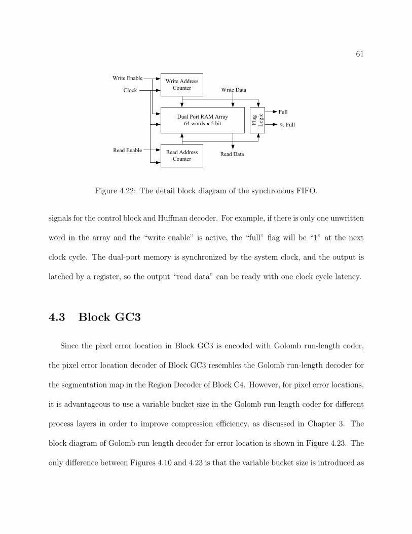
61
Write Address
Counter
Dual Port RAM Array
64 words 5 bit
Read Address
Counter
Flag
Logic
Write Enable
Clock
Read Enable
Write Data
Read Data
Full
% Full
Figure 4.22: The detail block diagram of the synchronous FIFO.
signals for the control block and Huffman decoder. For example, if there is only one unwritten
word in the array and the “write enable” is active, the “full” flag will be “1” at the next
clock cycle. The dual-port memory is synchronized by the system clock, and the output is
latched by a register, so the output “read data” can be ready with one clock cycle latency.
4.3 Block GC3
Since the pixel error location in Block GC3 is encoded with Golomb run-length coder,
the pixel error location decoder of Block GC3 resembles the Golomb run-length decoder for
the segmentation map in the Region Decoder of Block C4. However, for pixel error locations,
it is advantageous to use a variable bucket size in the Golomb run-length coder for different
process layers in order to improve compression efficiency, as discussed in Chapter 3. The
block diagram of Golomb run-length decoder for error location is shown in Figure 4.23. The
only difference between Figures 4.10 and 4.23 is that the variable bucket size is introduced as
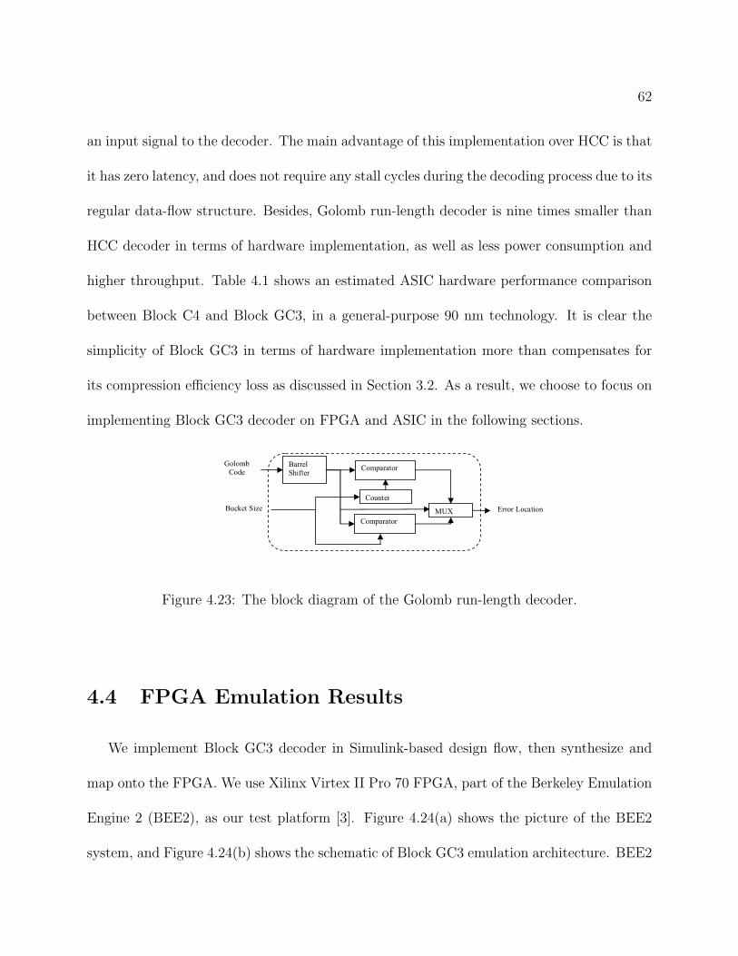
62
an input signal to the decoder. The main advantage of this implementation over HCC is that
it has zero latency, and does not require any stall cycles during the decoding process due to its
regular data-flow structure. Besides, Golomb run-length decoder is nine times smaller than
HCC decoder in terms of hardware implementation, as well as less power consumption and
higher throughput. Table 4.1 shows an estimated ASIC hardware performance comparison
between Block C4 and Block GC3, in a general-purpose 90 nm technology. It is clear the
simplicity of Block GC3 in terms of hardware implementation more than compensates for
its compression efficiency loss as discussed in Section 3.2. As a result, we choose to focus on
implementing Block GC3 decoder on FPGA and ASIC in the following sections.
Barrel Shifter
Counter
Comparator
Comparator
MUX
Golomb Code
Bucket Size Error Location
Figure 4.23: The block diagram of the Golomb run-length decoder.
4.4 FPGA Emulation Results
We implement Block GC3 decoder in Simulink-based design flow, then synthesize and
map onto the FPGA. We use Xilinx Virtex II Pro 70 FPGA, part of the Berkeley Emulation
Engine 2 (BEE2), as our test platform [3]. Figure 4.24(a) shows the picture of the BEE2
system, and Figure 4.24(b) shows the schematic of Block GC3 emulation architecture. BEE2
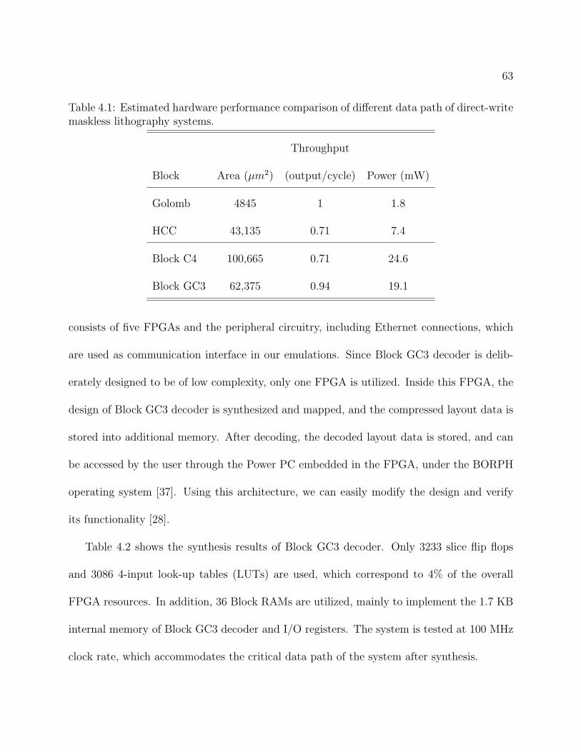
63
Table 4.1: Estimated hardware performance comparison of different data path of direct-writemaskless lithography systems.
Throughput
Block Area (�m2) (output/cycle) Power (mW)
Golomb 4845 1 1.8
HCC 43,135 0.71 7.4
Block C4 100,665 0.71 24.6
Block GC3 62,375 0.94 19.1
consists of five FPGAs and the peripheral circuitry, including Ethernet connections, which
are used as communication interface in our emulations. Since Block GC3 decoder is delib-
erately designed to be of low complexity, only one FPGA is utilized. Inside this FPGA, the
design of Block GC3 decoder is synthesized and mapped, and the compressed layout data is
stored into additional memory. After decoding, the decoded layout data is stored, and can
be accessed by the user through the Power PC embedded in the FPGA, under the BORPH
operating system [37]. Using this architecture, we can easily modify the design and verify
its functionality [28].
Table 4.2 shows the synthesis results of Block GC3 decoder. Only 3233 slice flip flops
and 3086 4-input look-up tables (LUTs) are used, which correspond to 4% of the overall
FPGA resources. In addition, 36 Block RAMs are utilized, mainly to implement the 1.7 KB
internal memory of Block GC3 decoder and I/O registers. The system is tested at 100 MHz
clock rate, which accommodates the critical data path of the system after synthesis.
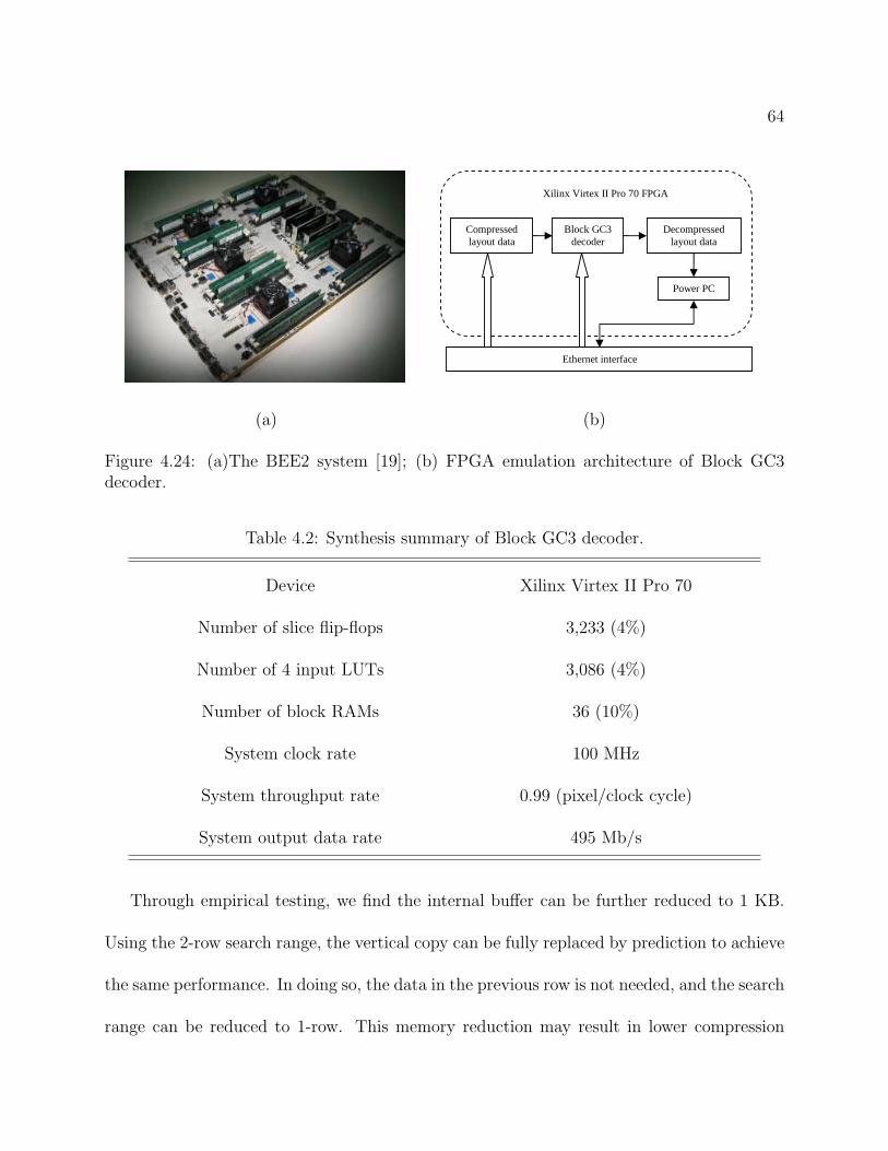
64
Block GC3 decoder
Compressed layout data
Decompressed layout data
Power PC
Ethernet interface
Xilinx Virtex II Pro 70 FPGA
(a) (b)
Figure 4.24: (a)The BEE2 system [19]; (b) FPGA emulation architecture of Block GC3decoder.
Table 4.2: Synthesis summary of Block GC3 decoder.
Device Xilinx Virtex II Pro 70
Number of slice flip-flops 3,233 (4%)
Number of 4 input LUTs 3,086 (4%)
Number of block RAMs 36 (10%)
System clock rate 100 MHz
System throughput rate 0.99 (pixel/clock cycle)
System output data rate 495 Mb/s
Through empirical testing, we find the internal buffer can be further reduced to 1 KB.
Using the 2-row search range, the vertical copy can be fully replaced by prediction to achieve
the same performance. In doing so, the data in the previous row is not needed, and the search
range can be reduced to 1-row. This memory reduction may result in lower compression
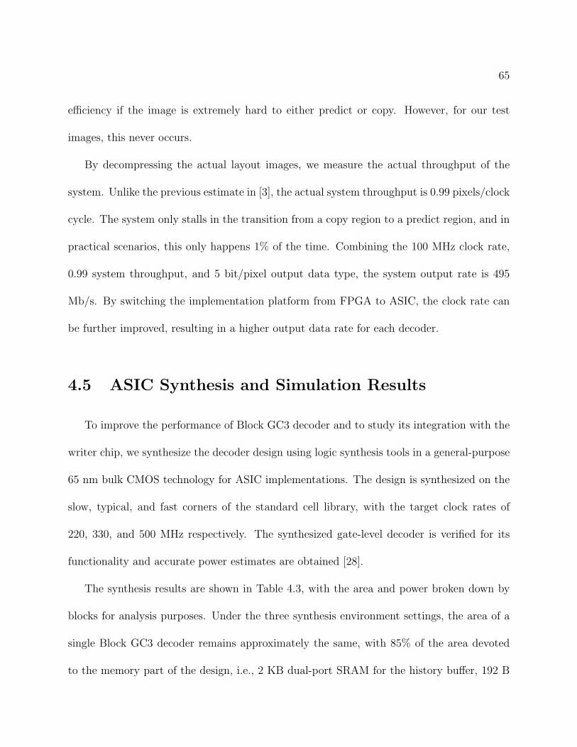
65
efficiency if the image is extremely hard to either predict or copy. However, for our test
images, this never occurs.
By decompressing the actual layout images, we measure the actual throughput of the
system. Unlike the previous estimate in [3], the actual system throughput is 0.99 pixels/clock
cycle. The system only stalls in the transition from a copy region to a predict region, and in
practical scenarios, this only happens 1% of the time. Combining the 100 MHz clock rate,
0.99 system throughput, and 5 bit/pixel output data type, the system output rate is 495
Mb/s. By switching the implementation platform from FPGA to ASIC, the clock rate can
be further improved, resulting in a higher output data rate for each decoder.
4.5 ASIC Synthesis and Simulation Results
To improve the performance of Block GC3 decoder and to study its integration with the
writer chip, we synthesize the decoder design using logic synthesis tools in a general-purpose
65 nm bulk CMOS technology for ASIC implementations. The design is synthesized on the
slow, typical, and fast corners of the standard cell library, with the target clock rates of
220, 330, and 500 MHz respectively. The synthesized gate-level decoder is verified for its
functionality and accurate power estimates are obtained [28].
The synthesis results are shown in Table 4.3, with the area and power broken down by
blocks for analysis purposes. Under the three synthesis environment settings, the area of a
single Block GC3 decoder remains approximately the same, with 85% of the area devoted
to the memory part of the design, i.e., 2 KB dual-port SRAM for the history buffer, 192 B
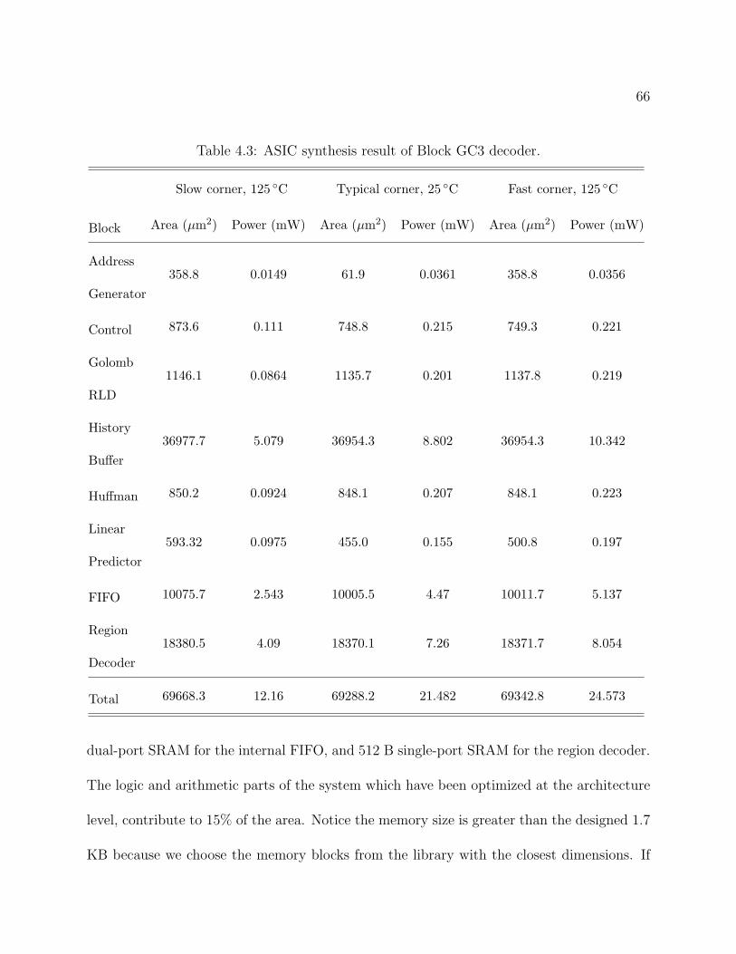
66
Table 4.3: ASIC synthesis result of Block GC3 decoder.
Slow corner, 125 ∘C Typical corner, 25 ∘C Fast corner, 125 ∘C
Block Area (�m2) Power (mW) Area (�m2) Power (mW) Area (�m2) Power (mW)
Address
Generator
358.8 0.0149 61.9 0.0361 358.8 0.0356
Control 873.6 0.111 748.8 0.215 749.3 0.221
Golomb
RLD
1146.1 0.0864 1135.7 0.201 1137.8 0.219
History
Buffer
36977.7 5.079 36954.3 8.802 36954.3 10.342
Huffman 850.2 0.0924 848.1 0.207 848.1 0.223
Linear
Predictor
593.32 0.0975 455.0 0.155 500.8 0.197
FIFO 10075.7 2.543 10005.5 4.47 10011.7 5.137
Region
Decoder
18380.5 4.09 18370.1 7.26 18371.7 8.054
Total 69668.3 12.16 69288.2 21.482 69342.8 24.573
dual-port SRAM for the internal FIFO, and 512 B single-port SRAM for the region decoder.
The logic and arithmetic parts of the system which have been optimized at the architecture
level, contribute to 15% of the area. Notice the memory size is greater than the designed 1.7
KB because we choose the memory blocks from the library with the closest dimensions. If
67
custom-designed memory blocks were used, the area of the decoder could have been further
reduced.
The memory blocks also contribute to the critical path of the system, namely the “history
buffer–linear predictor–control–history buffer” path as shown in Figure 4.1. Since this path
involves both the read and write processes of the dual-port memory, the access time of both
operations has to be considered, along with the propagation delays from other logic and
arithmetic operations. This results in a relatively slow clock rate for the 65 nm technology;
nevertheless, the impact may also be alleviated by applying custom-designed memory blocks.
The power consumption in Table 4.3 is estimated by decoding a poly layer layout image
and recording the switching activities of the decoder during the process. Intuitively, a faster
clock rate results in a higher switch activity; this phenomenon is reflected in the power
consumption, as the fast corner design consumes more power than the other two designs.
However, this number may vary from image to image, since for the sparse layouts or non-
critical layers of the layouts, the switching activity may be much lower than that of the poly
layer. In fact, if we use an average 25% switching activity factor to estimate the power, the
difference can be up to 75%.
Table 4.4 shows samples of power estimate using different environment settings and
switching activity factors (�). Notice the power estimate for decoding the poly layer image
is much higher than the power estimate assuming � = 0.25; in particular, the most discrep-
ancy happens in the address generator block, where the switching activity is much higher
than 25%. This is due to the incremental operation of the binary counter; the correspond-
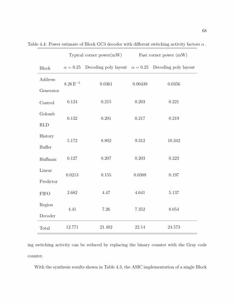
68
Table 4.4: Power estimate of Block GC3 decoder with different switching activity factors � .
Typical corner power(mW) Fast corner power (mW)
Block � = 0.25 Decoding poly layout � = 0.25 Decoding poly layout
Address
Generator
8.26E−5 0.0361 0.00439 0.0356
Control 0.124 0.215 0.203 0.221
Golomb
RLD
0.132 0.201 0.217 0.219
History
Buffer
5.172 8.802 9.312 10.342
Huffman 0.127 0.207 0.203 0.223
Linear
Predictor
0.0213 0.155 0.0388 0.197
FIFO 2.682 4.47 4.641 5.137
Region
Decoder
4.41 7.26 7.352 8.054
Total 12.771 21.482 22.14 24.573
ing switching activity can be reduced by replacing the binary counter with the Gray code
counter.
With the synthesis results shown in Table 4.3, the ASIC implementation of a single Block
69
GC3 decoder can achieve the output data rate up to 2.47 Gb/s. For 200 decoders running
in parallel, resulting in the total output rate of 500 Gb/s, or 3 wafer layers per hour, the
required area and power are 14mm2 and 5.4 W respectively. As compared to the direct-
write method, this results in a power saving of 24% with a minimal amount of hardware
overhead [4]. However, in terms of layout floorplanning, the aspect ratio of the decoder
layout has to be further determined, depending on different writer system architectures and
layout specifications, such as in [40] and [33].
4.6 Summary
In this chapter, we have shown the detailed implementation of Block C4 and Block GC3
decoder, with the schematic and operation of each blocks. Between these two designs, we
choose to implement Block GC3 in both FPGA and ASIC. For FPGA, a single Block GC3
decoder only utilizes 4% of the resources of a Xilinx Virtex Pro II 70 FPGA. The system
can run at 100 MHz, resulting in an output data rate of 495 Mb/s. We have also presented
the ASIC synthesis result of the design in the 65 nm technology, which results in a 0.07
mm2 design with the maximum output data rate of 2.47 Gb/s for a single decoder. Its
low hardware overhead and data flow architecture make it feasible for parallel processing of
direct-write lithography writing systems.
70
Chapter 5
Integrating Decoder with Maskless
Writing System
5.1 Introduction
In order to integrate the Block GC3 decoder with the writer system, we have to consider
the datapath between the decoder and the rest of the system. This includes buffering the
data from the I/O interface to the decoder, buffering the output of the decoder before it is
fed into the writer, and packaging the input data stream so that multiple input data streams
can share the same I/O interface. In addition, since the Block GC3 uses previous output
data to either predict or generate the current pixel value, proper error control is needed to
avoid the error propagation. These issues are discussed in this chapter.
71
5.2 Input/Output data buffering
In Block GC3 decoder, one bit in the input date stream is typically decoded into multiple
output pixel values, depending on the compression efficiency. In other words, the input data
rate is potentially lower than the output data rate by the compression ratio, resulting in
a fewer number of input data links and lower power consumption by the I/O interface. In
practice, this lower input data rate can only be achieved by buffering the input data on-chip
before it is read by the decoder. However, this also requires additional internal buffers of
the writer chip, which is what we are trying to avoid in the first place. In previous work, we
have proposed the on-chip buffer to be of the size
buffer size =image size
compression ratio, (5.1)
which suggests the entire 1024× 1024 compressed layout image to be stored in the memory
before being decoded [47]. Assuming the compression ratio of 10, this corresponds to 64
KB of internal buffer. Even though this number is not substantial, considering hundreds of
decoders running in parallel to achieve the projected output data rate, the scaled buffer size
may not be feasible. In addition, this buffer size may be an overestimate since the writer
system reads and writes the buffer simultaneously, in a first-in-first-out fashion. In this
case, the buffer may only be completely full at the very beginning of the decoding process,
resulting in a waste of the resources.
To circumvent the above problem, we propose to reduce the size of the input data buffer
72
to
buffer size = a× image size×(
1
compression ratio− 1
input data rate
)
. (5.2)
Unlike Eqn. (5.1), the buffer size in Eqn. (5.2) is a function of both the input and output rate
of the FIFO, and the size is reduced by taking the update speed into account. The constant
a, which is slightly greater than 1, is introduced to ensure the FIFO will not become empty.
For high compression ratio images, this buffer will always be almost full, since the input
data rate is higher than the compression ratio, which corresponds to the output data rate.
In this case, the input data link is on only when the FIFO is not full. On the other hand,
for low compression ratio images, the FIFO is slowly drained to be empty; this is because
its output data rate is higher than its input data rate, while the input data link is always
on, running at the designed input data rate. In this architecture, after decomposing the
rasterized layout into a series of images, we need to arrange the layout images so that not
all low compression ratio images are clustered together, resulting in an empty input FIFO.
The arrangement strategy for layout images was presented in [47], and can be performed at
the encoding stage.
5.3 Control of Error Propagation
In Block GC3 algorithm, both copy and predict schemes use the previous pixel values
stored in the history buffer to generate the current pixel value. If the stored pixel value
is altered during the read/write process of the history buffer, the error propagates to the
73
remaining part of the image. To solve this problem, we have to consider error control
strategies. First, the history buffer has to be refreshed for every new image. Although Block
GC3 algorithm is suitable for stream coding, i.e., using the history buffer of the previous
image to code the current one, the error can also propagate from the previous image in
the same fashion. Therefore, refreshing of the history buffer would confine the error to the
image boundaries. This results in some encoding overhead at the beginning of the images,
and lower compression efficiency as compared to stream coding. However, considering the
1-row and 2-row buffer cases, the overhead and compression efficiency loss are negligible.
Besides setting up the boundaries of the images, we can further reduce error by applying
error control code (ECC) to the history buffer. Hamming (7, 4) code is a simple error
control code, which has been implemented in hardware in the literature [26] [43]. In this
code, 4 bits of data are coded with 3 extra parity bits to construct a 7-bit code. While
decoding the Hamming code, one error bit in the code can be identified and corrected, and
two error bits can be detected by the decoder. In the history buffer of Block GC3, we can
apply the Hamming (7, 4) code to encode the four most significant bits of the 5-bit pixel
value, resulting in a 8-bit code for every pixel, which can be stored into a typical memory
design without wasting resources. While reading the pixel value from the history buffer, the
single-bit error can be corrected. A schematic of possible history buffer design is shown in
Figure 5.1. Depending on the retention ability of the memory, this may effectively reduce
the error propagation.
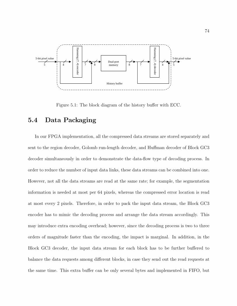
74
Ha
mm
ing (7
, 4) en
code
r
5-bit pixel value
5 4 7Dual-port memory 8
Ha
mm
ing (7
, 4) de
code
r
7 4 58
5-bit pixel value
History buffer
Figure 5.1: The block diagram of the history buffer with ECC.
5.4 Data Packaging
In our FPGA implementation, all the compressed data streams are stored separately and
sent to the region decoder, Golomb run-length decoder, and Huffman decoder of Block GC3
decoder simultaneously in order to demonstrate the data-flow type of decoding process. In
order to reduce the number of input data links, these data streams can be combined into one.
However, not all the data streams are read at the same rate; for example, the segmentation
information is needed at most per 64 pixels, whereas the compressed error location is read
at most every 2 pixels. Therefore, in order to pack the input data stream, the Block GC3
encoder has to mimic the decoding process and arrange the data stream accordingly. This
may introduce extra encoding overhead; however, since the decoding process is two to three
orders of magnitude faster than the encoding, the impact is marginal. In addition, in the
Block GC3 decoder, the input data stream for each block has to be further buffered to
balance the data requests among different blocks, in case they send out the read requests at
the same time. This extra buffer can be only several bytes and implemented in FIFO, but
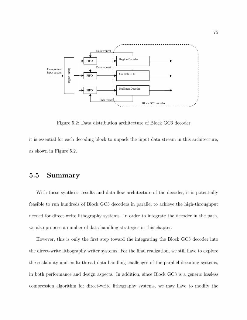
75
Inpu
t bu
ffer
FIFO
Region Decoder
Golomb RLD
Huffman Decoder
Compressed input stream
FIFO
FIFO
Data request
Data request
Data request Block GC3 decoder
Figure 5.2: Data distribution architecture of Block GC3 decoder
it is essential for each decoding block to unpack the input data stream in this architecture,
as shown in Figure 5.2.
5.5 Summary
With these synthesis results and data-flow architecture of the decoder, it is potentially
feasible to run hundreds of Block GC3 decoders in parallel to achieve the high-throughput
needed for direct-write lithography systems. In order to integrate the decoder in the path,
we also propose a number of data handling strategies in this chapter.
However, this is only the first step toward the integrating the Block GC3 decoder into
the direct-write lithography writer systems. For the final realization, we still have to explore
the scalability and multi-thread data handling challenges of the parallel decoding systems,
in both performance and design aspects. In addition, since Block GC3 is a generic lossless
compression algorithm for direct-write lithography systems, we may have to modify the

76
algorithm to accommodate the specifications of different writing technologies and layout
images while keeping the decoder complexity low. In the next chapter, we will provide one
such writing system as a case study.
77
Chapter 6
Block RGC3: Lossless Compression
Algorithm for Rotary Writing
Systems
6.1 Introduction
A new maskless direct-write lithography system, called Reflective Electron Beam Lithog-
raphy (REBL), is currently under development at KLA-Tencor [33]. In this system, the
layout patterns are written on a rotary writing stage, resulting in layout data which is ro-
tated at arbitrary angles with respect to the pixel grid. Moreover, the data is subjected to
E-beam proximity correction effects. We have empirically found that applying the Block
GC3 algorithm to E-beam proximity corrected and rotated layout data results in poor com-
78
pression efficiency far below those obtained on Manhattan geometry and without E-beam
proximity correction. Consequently, Block GC3 needs to be modified to accommodate the
characteristics of REBL data while maintaining a low-complexity decoder for the hardware
implementation. In this chapter, we modify Block GC3 in a number of ways in order to
make it applicable to the REBL system; we refer to this new algorithm as Block Rotated
Golomb Context Copy Coding (Block RGC3).
In this chapter, we first introduce the data-delivery path of the REBL system and the
requirements it imposes on the compression technique. We then describe the modifications
resulting in Block RGC3; these include an alternate copy algorithm, a finer block size,
and segmentation information compression, which better suit rotated layout patterns. We
also characterizes the additional encoding complexity required to implement our proposed
changes to Block GC3.
6.2 Datapath for REBL System
The REBL system is visualized in Figure 6.1(a), and detailed in [33] [32]. REBL’s goal
is to produce high resolution of electron-beam lithography while maintaining throughputs
comparable to those of today’s optical lithography systems. The Digital Pattern Generator
(DPG) uses reflective electron optics to constantly shape the electron beam as it scans across
the wafers, which are located on a rotary stage shown in Figure 6.1(b). This chapter focuses
on the data delivery path of the REBL system, which constrains the compression hardware
implementation. As shown in Figure 6.2, the compressed layout data is decoded by Block
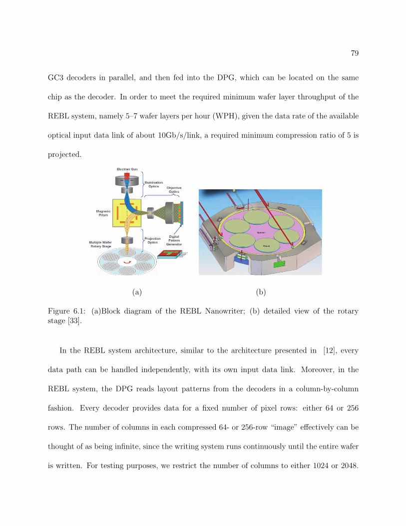
79
GC3 decoders in parallel, and then fed into the DPG, which can be located on the same
chip as the decoder. In order to meet the required minimum wafer layer throughput of the
REBL system, namely 5–7 wafer layers per hour (WPH), given the data rate of the available
optical input data link of about 10Gb/s/link, a required minimum compression ratio of 5 is
projected.
(a) (b)
Figure 6.1: (a)Block diagram of the REBL Nanowriter; (b) detailed view of the rotarystage [33].
In the REBL system architecture, similar to the architecture presented in [12], every
data path can be handled independently, with its own input data link. Moreover, in the
REBL system, the DPG reads layout patterns from the decoders in a column-by-column
fashion. Every decoder provides data for a fixed number of pixel rows: either 64 or 256
rows. The number of columns in each compressed 64- or 256-row “image” effectively can be
thought of as being infinite, since the writing system runs continuously until the entire wafer
is written. For testing purposes, we restrict the number of columns to either 1024 or 2048.
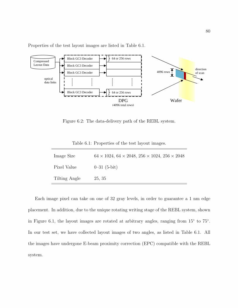
80
Properties of the test layout images are listed in Table 6.1.
Compressed Layout Data
Block GC3 Decoder
Block GC3 Decoder
Block GC3 Decoder
64 or 256 rows
.......
optical data links
Wafer
4096 rows direction of scan
Block GC3 Decoder
.......
.......
.......
64 or 256 rows
DPG (4096 total rows)
Figure 6.2: The data-delivery path of the REBL system.
Table 6.1: Properties of the test layout images.
Image Size 64× 1024, 64× 2048, 256× 1024, 256× 2048
Pixel Value 0–31 (5-bit)
Tilting Angle 25, 35
Each image pixel can take on one of 32 gray levels, in order to guarantee a 1 nm edge
placement. In addition, due to the unique rotating writing stage of the REBL system, shown
in Figure 6.1, the layout images are rotated at arbitrary angles, ranging from 15∘ to 75∘.
In our test set, we have collected layout images of two angles, as listed in Table 6.1. All
the images have undergone E-beam proximity correction (EPC) compatible with the REBL
system.
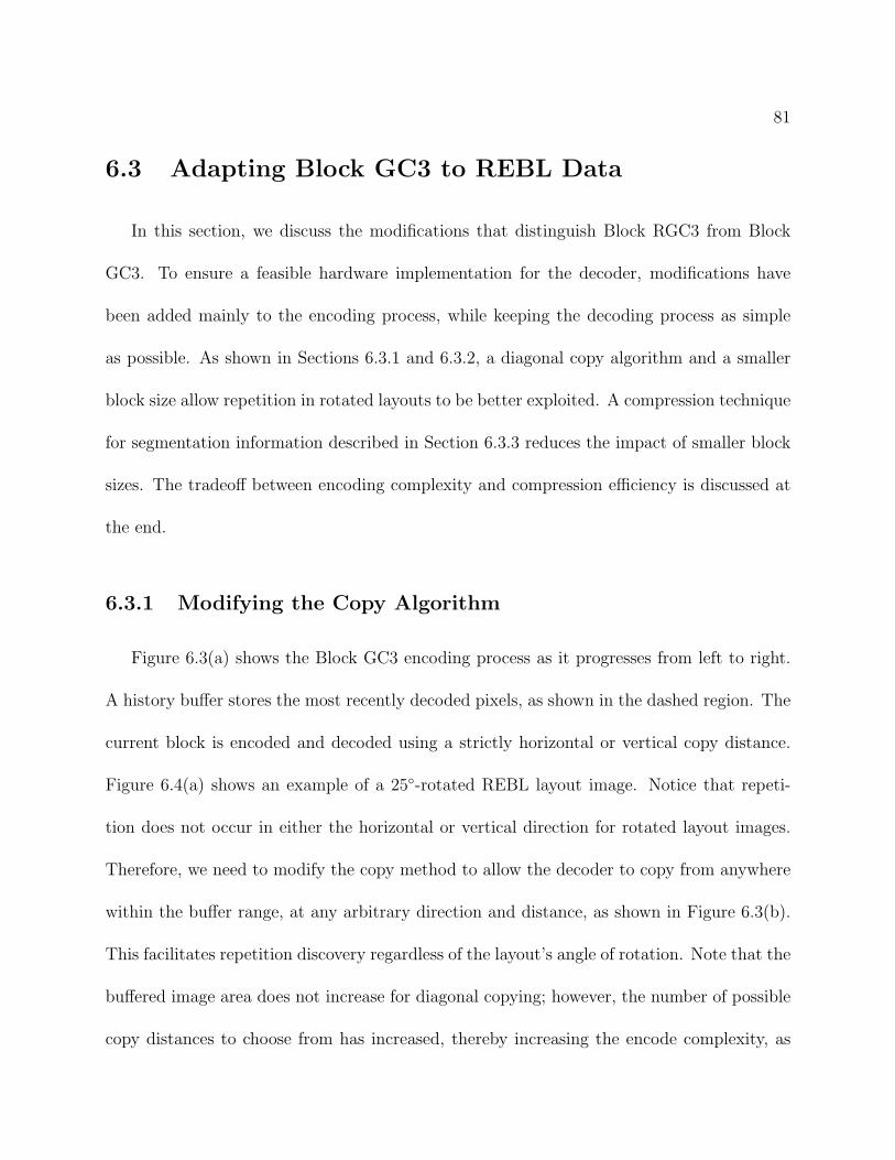
81
6.3 Adapting Block GC3 to REBL Data
In this section, we discuss the modifications that distinguish Block RGC3 from Block
GC3. To ensure a feasible hardware implementation for the decoder, modifications have
been added mainly to the encoding process, while keeping the decoding process as simple
as possible. As shown in Sections 6.3.1 and 6.3.2, a diagonal copy algorithm and a smaller
block size allow repetition in rotated layouts to be better exploited. A compression technique
for segmentation information described in Section 6.3.3 reduces the impact of smaller block
sizes. The tradeoff between encoding complexity and compression efficiency is discussed at
the end.
6.3.1 Modifying the Copy Algorithm
Figure 6.3(a) shows the Block GC3 encoding process as it progresses from left to right.
A history buffer stores the most recently decoded pixels, as shown in the dashed region. The
current block is encoded and decoded using a strictly horizontal or vertical copy distance.
Figure 6.4(a) shows an example of a 25∘-rotated REBL layout image. Notice that repeti-
tion does not occur in either the horizontal or vertical direction for rotated layout images.
Therefore, we need to modify the copy method to allow the decoder to copy from anywhere
within the buffer range, at any arbitrary direction and distance, as shown in Figure 6.3(b).
This facilitates repetition discovery regardless of the layout’s angle of rotation. Note that the
buffered image area does not increase for diagonal copying; however, the number of possible
copy distances to choose from has increased, thereby increasing the encode complexity, as
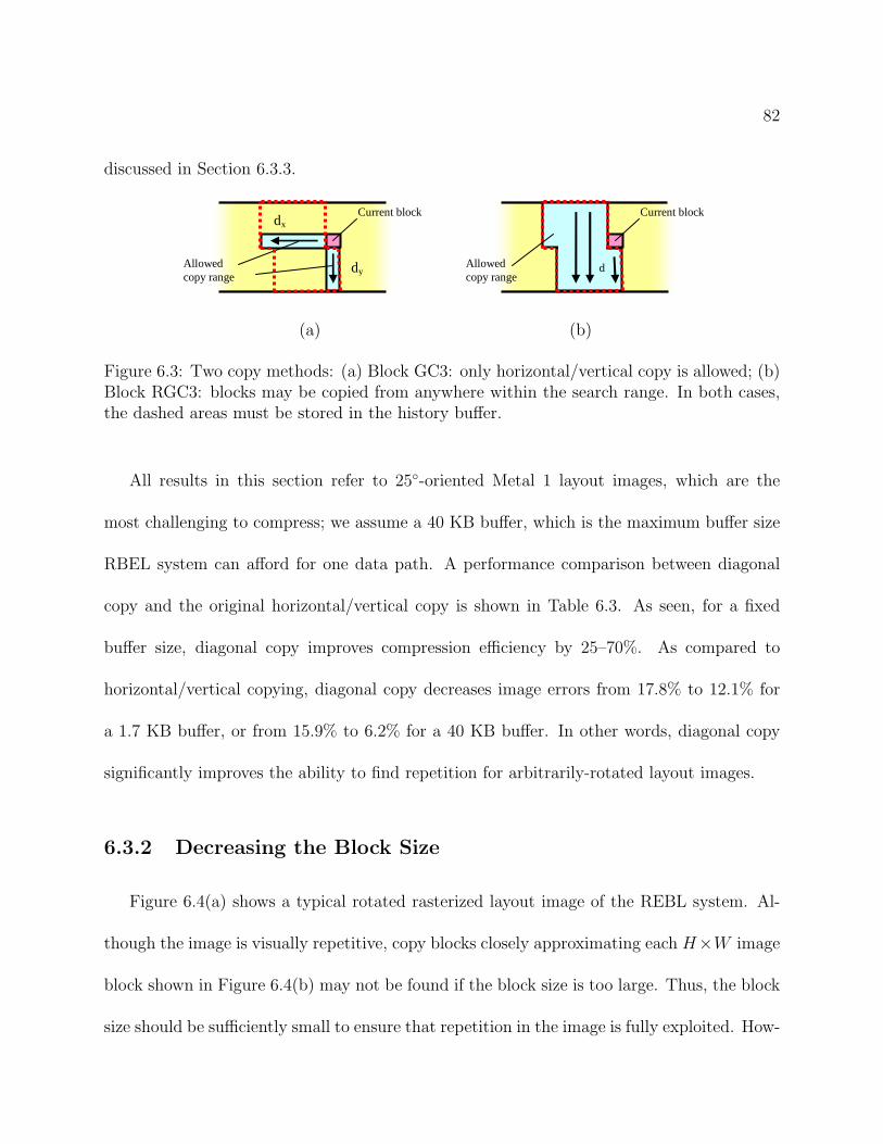
82
discussed in Section 6.3.3.
dx
dyAllowed copy range
Current block
Allowed copy range
Current block
d
x
y
(a) (b)
Figure 6.3: Two copy methods: (a) Block GC3: only horizontal/vertical copy is allowed; (b)Block RGC3: blocks may be copied from anywhere within the search range. In both cases,the dashed areas must be stored in the history buffer.
All results in this section refer to 25∘-oriented Metal 1 layout images, which are the
most challenging to compress; we assume a 40 KB buffer, which is the maximum buffer size
RBEL system can afford for one data path. A performance comparison between diagonal
copy and the original horizontal/vertical copy is shown in Table 6.3. As seen, for a fixed
buffer size, diagonal copy improves compression efficiency by 25–70%. As compared to
horizontal/vertical copying, diagonal copy decreases image errors from 17.8% to 12.1% for
a 1.7 KB buffer, or from 15.9% to 6.2% for a 40 KB buffer. In other words, diagonal copy
significantly improves the ability to find repetition for arbitrarily-rotated layout images.
6.3.2 Decreasing the Block Size
Figure 6.4(a) shows a typical rotated rasterized layout image of the REBL system. Al-
though the image is visually repetitive, copy blocks closely approximating each H×W image
block shown in Figure 6.4(b) may not be found if the block size is too large. Thus, the block
size should be sufficiently small to ensure that repetition in the image is fully exploited. How-
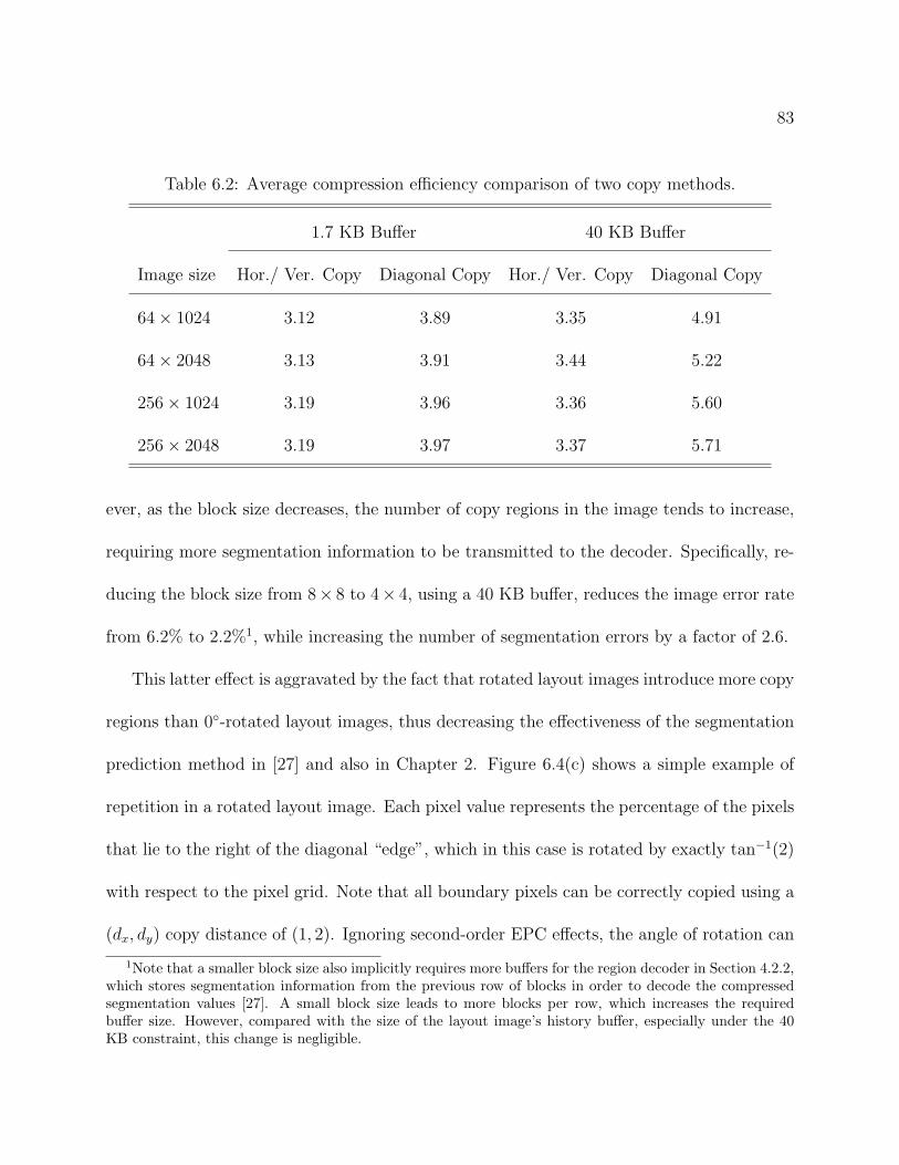
83
Table 6.2: Average compression efficiency comparison of two copy methods.
1.7 KB Buffer 40 KB Buffer
Image size Hor./ Ver. Copy Diagonal Copy Hor./ Ver. Copy Diagonal Copy
64× 1024 3.12 3.89 3.35 4.91
64× 2048 3.13 3.91 3.44 5.22
256× 1024 3.19 3.96 3.36 5.60
256× 2048 3.19 3.97 3.37 5.71
ever, as the block size decreases, the number of copy regions in the image tends to increase,
requiring more segmentation information to be transmitted to the decoder. Specifically, re-
ducing the block size from 8× 8 to 4× 4, using a 40 KB buffer, reduces the image error rate
from 6.2% to 2.2%1, while increasing the number of segmentation errors by a factor of 2.6.
This latter effect is aggravated by the fact that rotated layout images introduce more copy
regions than 0∘-rotated layout images, thus decreasing the effectiveness of the segmentation
prediction method in [27] and also in Chapter 2. Figure 6.4(c) shows a simple example of
repetition in a rotated layout image. Each pixel value represents the percentage of the pixels
that lie to the right of the diagonal “edge”, which in this case is rotated by exactly tan−1(2)
with respect to the pixel grid. Note that all boundary pixels can be correctly copied using a
(dx, dy) copy distance of (1, 2). Ignoring second-order EPC effects, the angle of rotation can
1Note that a smaller block size also implicitly requires more buffers for the region decoder in Section 4.2.2,which stores segmentation information from the previous row of blocks in order to decode the compressedsegmentation values [27]. A small block size leads to more blocks per row, which increases the requiredbuffer size. However, compared with the size of the layout image’s history buffer, especially under the 40KB constraint, this change is negligible.
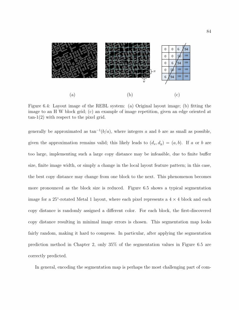
84
H
W
0
0
0
0
0
0
6
50
94
100
6
50
94
100
6 94 100
100
100
100
(a) (b) (c)
Figure 6.4: Layout image of the REBL system: (a) Original layout image; (b) fitting theimage to an H W block grid; (c) an example of image repetition, given an edge oriented attan-1(2) with respect to the pixel grid.
generally be approximated as tan−1(b/a), where integers a and b are as small as possible,
given the approximation remains valid; this likely leads to (dx, dy) = (a, b). If a or b are
too large, implementing such a large copy distance may be infeasible, due to finite buffer
size, finite image width, or simply a change in the local layout feature pattern; in this case,
the best copy distance may change from one block to the next. This phenomenon becomes
more pronounced as the block size is reduced. Figure 6.5 shows a typical segmentation
image for a 25∘-rotated Metal 1 layout, where each pixel represents a 4 × 4 block and each
copy distance is randomly assigned a different color. For each block, the first-discovered
copy distance resulting in minimal image errors is chosen. This segmentation map looks
fairly random, making it hard to compress. In particular, after applying the segmentation
prediction method in Chapter 2, only 35% of the segmentation values in Figure 6.5 are
correctly predicted.
In general, encoding the segmentation map is perhaps the most challenging part of com-
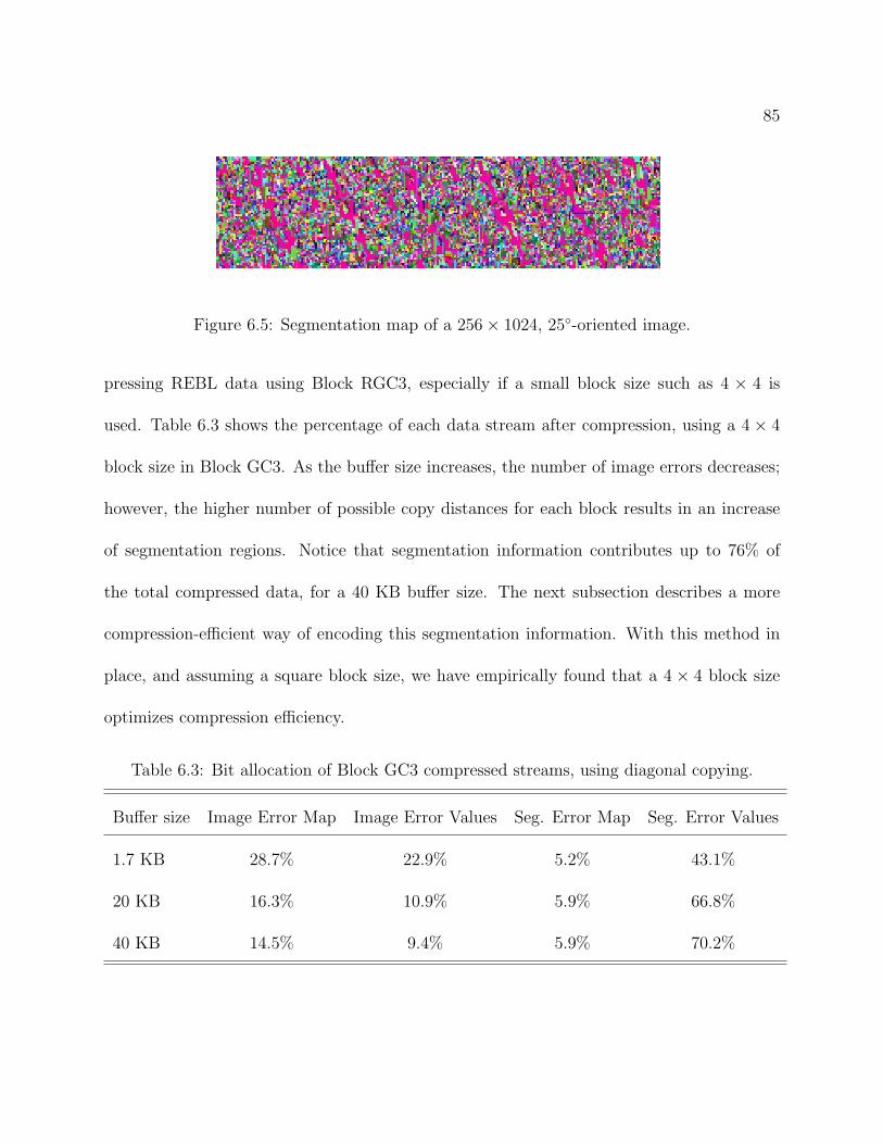
85
Figure 6.5: Segmentation map of a 256× 1024, 25∘-oriented image.
pressing REBL data using Block RGC3, especially if a small block size such as 4 × 4 is
used. Table 6.3 shows the percentage of each data stream after compression, using a 4 × 4
block size in Block GC3. As the buffer size increases, the number of image errors decreases;
however, the higher number of possible copy distances for each block results in an increase
of segmentation regions. Notice that segmentation information contributes up to 76% of
the total compressed data, for a 40 KB buffer size. The next subsection describes a more
compression-efficient way of encoding this segmentation information. With this method in
place, and assuming a square block size, we have empirically found that a 4 × 4 block size
optimizes compression efficiency.
Table 6.3: Bit allocation of Block GC3 compressed streams, using diagonal copying.
Buffer size Image Error Map Image Error Values Seg. Error Map Seg. Error Values
1.7 KB 28.7% 22.9% 5.2% 43.1%
20 KB 16.3% 10.9% 5.9% 66.8%
40 KB 14.5% 9.4% 5.9% 70.2%
86
6.3.3 Compression for Segmentation Information
As shown in Figure 6.5 and Table 6.3, the segmentation information looks random, and as
such, could attribute to the major part of the compressed data stream. In order to improve
the performance of Block RGC3, the segmentation information has to be further compressed.
There are several different approaches: First, we can apply different segmentation predic-
tion algorithms to predict the copy distance to accommodate the angle-oriented segmentation
map, as suggested in [18], [15], and [45]. However, such prediction methods may introduce
extra buffers to store more than one row of blocks, and the effect can be marginal. This is
again due to the randomness of the segmentation map. As a result, to maintain the simplicity
of the decoder, we keep the segmentation prediction methods shown in Figure 4.5.
The next strategy is to reduce the randomness of the segmentation map, i.e., enforce
the spatial coherence of the segmentation map. Notice that the map is an artificial image,
and the pixel values represent different copy distances. However, for each block, there may
be multiple copy distances resulting in the minimum image errors. In that sense, we can
select the copy distances carefully, and grow “regions” consisting of one or more adjacent
blocks, each assigned the same copy distance. By creating large regions, the segmentation
map can be simplified. Regions can be grown in 2-dimensional way. The optimal region-
growing metric is to minimize the total number of 2-D regions, assuming a known fixed
number of image errors for each block. However, this problem is NP-complete, even if the
number of image errors per block is already known, as we have shown in Appendix A. As a
result, if we want to apply 2-D region growing, the heuristic algorithm again makes marginal
87
improvement. An alternative is to grow 1-D regions after first assuming each block contains
minimal image errors; the related discussion can be found in [8] and [7].
Finally, in contrast to Block GC3, the segmentation errors in Block RGC3 have to be
compressed before sending to the decoder; we apply Huffman codes to compress this. How-
ever, in this step, we split the horizontal copy distance (dx) and vertical copy distance (dy)
into two streams and code them separately. The reason for this approach is simple: the size
of the Huffman table is proportional to p log2 p, where p is the maximum value of the stream.
Given a 40 KB buffer, the maximum copy distance is 216, resulting in a 128 KB Huffman
table, which is not practical; whereas the size of two Huffman tables with maximum copy
distance 28 is 0.25 KB, which is again negligible for the REBL system. The compression
efficiency of applying entropy coding is shown in Table 6.4. Notice the major improvement
resulting from applying Huffman code to the segmentation information, especially for larger
image sizes.
6.3.4 Impact on Encoding Complexity
By allowing diagonal copying, the encoder essentially compares each pixel with the pix-
els associated with each available copy distance. Thus, this portion of the encoding time
is independent of the input image pattern. The image is both encoded and decoded in
a column-by-column fashion. For Block RGC3, the number of possible copy distances
per block is dx max × dy max, where dy max typically equals the height of the image and
dx max = buffer size/dy max; in contrast, for Block GC3’s horizontal/vertical copying, the
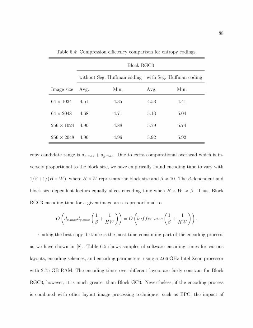
88
Table 6.4: Compression efficiency comparison for entropy codings.
Block RGC3
without Seg. Huffman coding with Seg. Huffman coding
Image size Avg. Min. Avg. Min.
64× 1024 4.51 4.35 4.53 4.41
64× 2048 4.68 4.71 5.13 5.04
256× 1024 4.90 4.88 5.79 5.74
256× 2048 4.96 4.96 5.92 5.92
copy candidate range is dx max + dy max. Due to extra computational overhead which is in-
versely proportional to the block size, we have empirically found encoding time to vary with
1/�+1/(H×W ), where H×W represents the block size and � ≈ 10. The �-dependent and
block size-dependent factors equally affect encoding time when H × W ≈ �. Thus, Block
RGC3 encoding time for a given image area is proportional to
O
(
dx maxdy max
(
1
�+
1
HW
))
= O
(
buffer size
(
1
�+
1
HW
))
.
Finding the best copy distance is the most time-consuming part of the encoding process,
as we have shown in [8]. Table 6.5 shows samples of software encoding times for various
layouts, encoding schemes, and encoding parameters, using a 2.66 GHz Intel Xeon processor
with 2.75 GB RAM. The encoding times over different layers are fairly constant for Block
RGC3, however, it is much greater than Block GC3. Nevertheless, if the encoding process
is combined with other layout image processing techniques, such as EPC, the impact of
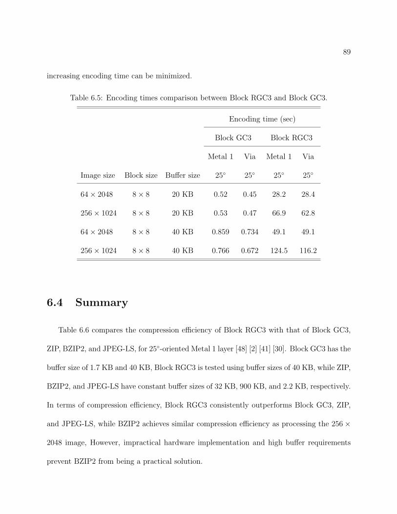
89
increasing encoding time can be minimized.
Table 6.5: Encoding times comparison between Block RGC3 and Block GC3.
Encoding time (sec)
Block GC3 Block RGC3
Metal 1 Via Metal 1 Via
Image size Block size Buffer size 25∘ 25∘ 25∘ 25∘
64× 2048 8× 8 20 KB 0.52 0.45 28.2 28.4
256× 1024 8× 8 20 KB 0.53 0.47 66.9 62.8
64× 2048 8× 8 40 KB 0.859 0.734 49.1 49.1
256× 1024 8× 8 40 KB 0.766 0.672 124.5 116.2
6.4 Summary
Table 6.6 compares the compression efficiency of Block RGC3 with that of Block GC3,
ZIP, BZIP2, and JPEG-LS, for 25∘-oriented Metal 1 layer [48] [2] [41] [30]. Block GC3 has the
buffer size of 1.7 KB and 40 KB, Block RGC3 is tested using buffer sizes of 40 KB, while ZIP,
BZIP2, and JPEG-LS have constant buffer sizes of 32 KB, 900 KB, and 2.2 KB, respectively.
In terms of compression efficiency, Block RGC3 consistently outperforms Block GC3, ZIP,
and JPEG-LS, while BZIP2 achieves similar compression efficiency as processing the 256×
2048 image, However, impractical hardware implementation and high buffer requirements
prevent BZIP2 from being a practical solution.
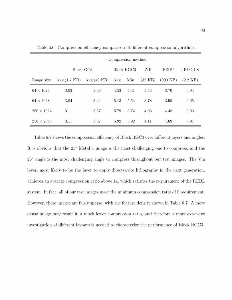
90
Table 6.6: Compression efficiency comparison of different compression algorithms.
Compression method
Block GC3 Block RGC3 ZIP BZIP2 JPEG-LS
Image size Avg.(1.7 KB) Avg.(40 KB) Avg. Min. (32 KB) (900 KB) (2.2 KB)
64× 1024 3.03 3.36 4.53 4.41 3.53 3.70 0.94
64× 2048 3.04 3.44 5.13 5.54 3.78 3.95 0.95
256× 1024 3.11 3.37 5.79 5.74 4.03 4.48 0.96
256× 2048 3.11 3.37 5.92 5.92 4.11 4.69 0.97
Table 6.7 shows the compression efficiency of Block RGC3 over different layers and angles.
It is obvious that the 25∘ Metal 1 image is the most challenging one to compress, and the
25∘ angle is the most challenging angle to compress throughout our test images. The Via
layer, most likely to be the layer to apply direct-write lithography in the next generation,
achieves an average compression ratio above 14, which satisfies the requirement of the REBL
system. In fact, all of our test images meet the minimum compression ratio of 5 requirement.
However, these images are fairly sparse, with the feature density shown in Table 6.7. A more
dense image may result in a much lower compression ratio, and therefore a more extensive
investigation of different layouts is needed to characterize the performance of Block RGC3.
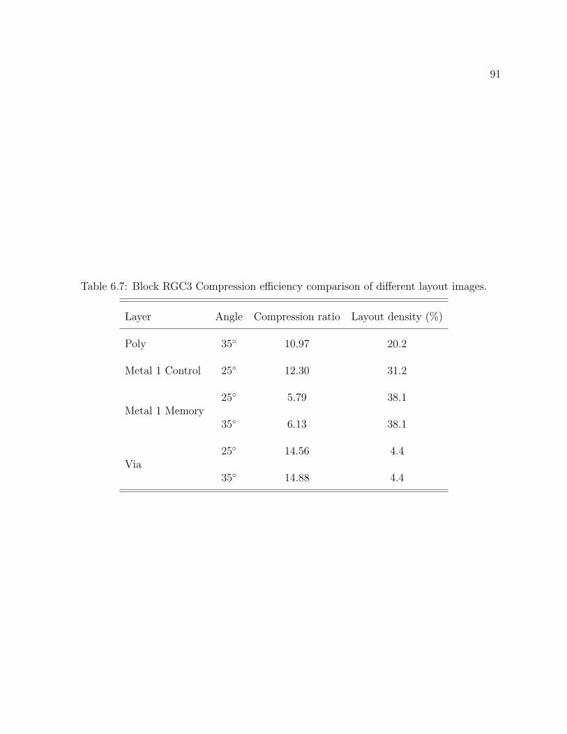
91
Table 6.7: Block RGC3 Compression efficiency comparison of different layout images.
Layer Angle Compression ratio Layout density (%)
Poly 35∘ 10.97 20.2
Metal 1 Control 25∘ 12.30 31.2
Metal 1 Memory25∘ 5.79 38.1
35∘ 6.13 38.1
Via25∘ 14.56 4.4
35∘ 14.88 4.4
92
Chapter 7
Conclusions and Future Work
Maskless lithography has been proposed as an alternative to optical lithography in order
to reduce the cost of the mask sets. However, to realize this direct-write technique, several
issues need to be addressed, including manufacturing micromirror array writing system using
MEMS, correcting proximity effect causing by the EUV and E-beam sources, controlling the
sources with desired degrees of freedom, actuating the micromirror array using mix signal
circuits, etc. Among them, the data delivery problem, transmitting the data from external
storage devices to the writer system for real-time update, is a bottleneck for realistic data
throughput of direct-write lithography systems. To this end, we have proposed to losslessly
compress the data beforehand, transmit the compressed data, and decompress it on-the-fly
in the writer chip. This implies the compression algorithm has to be asymmetric, i.e., the
decoder has to be simple and implementable in hardware with minimal overhead, while the
overall compression efficiency must be large enough to reduce the transmission and storage
93
overhead to a manageable level.
In this thesis, I have presented a lossless compression algorithm, Block Golomb Context-
Copy Code (GC3), that is implementable in hardware. The compression efficiency of Block
GC3 outperforms all existing lossless data compression algorithms, including LZ, ZIP, BZIP2,
JPEG-LS, Huffman, and run-length coding, with the decoder buffer of only 1.7 KB. Although
it has a 10–15% efficiency loss as compared to the previously proposed Block C4 algorithm, I
have shown Block GC3 achieves a much simpler hardware decoder design, thus compensating
for the compression efficiency loss.
I also have presented hardware design for Block GC3 decoder, along with the FPGA and
ASIC synthesis and simulation results. I have shown that Block GC3 results in a simple
digital circuit. A single Block GC3 decoder only utilizes 4% of the resources of a Xilinx
Virtex Pro II 70 FPGA. The system can run at 100 MHz, resulting in an output data rate of
495 Mb/s. Meanwhile, the corresponding ASIC synthesis in the 65 nm technology results in
an area of 0.07mm2 with the maximum output data rate of 2.47 Gb/s for a single decoder.
For 200 decoders running in parallel, resulting in the total output data rate of 500 Gb/s, or
3 wafer layers per hour, the required area and power are 14mm2 and 5.4 W respectively. As
compared to the direct-write method, this results in a power saving of 24% with a minimal
amount of hardware overhead [4]. With these synthesis results and data-flow architecture
of the decoder, it is potentially feasible to run hundreds Block GC3 decoders in parallel to
achieve the high-throughput needed for direct-write lithography systems.
To integrate the decoder into the writer chip, I have proposed several data handling
94
strategies for the data path. Regarding on-chip input FIFO buffering, the input data rate
can be reduced with a smaller memory as compared to our previous work [10], by utilizing
the simultaneous read/write property of FIFO. Meanwhile, with additional output data
buffering, the data between multiple decoders and writer devices can be synchronized, so
that multiple decoders can run in their own data flow without jeopardizing the final output.
In addition, error propagation control techniques such as memory refreshing and Hamming
code are introduced to minimize the impact of error propagation caused by imperfect data
retention ability of the memory. Finally, input data stream packaging is proposed to reduce
the number of input data streams, which can also reduce the I/O complexity if multiple
decoders are applied. This hardware data path implementation is independent of the writer
systems or data link types, and can be integrated with arbitrary direct-write lithography
systems.
To investigate the integration of Block GC3 with a real direct-write lithography system,
I have applied Block GC3 to the reflective electron-beam lithography (REBL) system, devel-
oped by KLA-Tencor [33] [32]. Two characteristic features of the REBL system are a rotary
stage resulting in arbitrarily-rotated layout imagery, and E-beam corrections prior to writ-
ing the data, both of which present significant challenges to lossless compression algorithms.
Together, these effects reduce the effectiveness of both the copy and predict compression
methods within Block GC3.
To deal with these challenges, I have proposed technique Block RGC3, which divides
the image into a grid of two-dimensional “blocks” of pixels, each of which is copied from a
95
specified location in a history buffer of recently-decoded pixels. However, in Block RGC3
the number of possible copy locations is significantly increased, so as to allow repetition
to be discovered along any orientation, rather than horizontal or vertical. Also, by copying
smaller groups of pixels at a time, repetition in layout patterns is easier to be found and taken
advantage of. As a side effect, this increases the total number of copy locations to transmit;
to overcome this, I have presented several strategies to reduce the transmitted data volume,
thereby improving compression efficiency. I have characterized the performance of Block
RGC3 in terms of compression efficiency and encoding complexity on a number of rotated
Metal 1, Poly, and Via layouts at various angles, and shown that Block RGC3 provides higher
compression efficiency than existing lossless compression algorithms for rotated layouts.
Through this work, I have presented Block GC3 as a solution for the data delivery issue of
direct-write lithography systems. However, since Block GC3 is a generic lossless compression
algorithm for direct-write lithography systems, the algorithm may need to be modified to
accommodate the specifics of different writer technologies and layout images while keeping
the decoder complexity low. Extensive testing over different layouts and layers is needed
when specifically targeting a given writing system [47].
The integration of decoder and writer chip poses additional challenges. For example,
we need to investigate the scalability and multi-thread data handling issues of the parallel
decoding systems when hundreds of decoders are on the same chip. In this case, it is
impossible to manually place the memory blocks at the floor-planning stage, and therefore
an automatic system or a inter-core memory sharing strategy is needed.
96
On the algorithmic side, Block GC3 also leaves some open questions. For example, can we
find a better segmentation algorithm to reduce the number of copy regions? In addition, after
we find a segmentation, is there a better way to code it so the size of the compressed data
can be reduced? The 1-D region growing method in [8] provided a possible solution to reduce
the complexity of the segmentation map; however, a generalized two-dimensional solution
and a better data representation algorithm may still improve the compression efficiency.
Besides direct-write lithography application, the lossless compression algorithm can also
be applied to compress natural images and videos, as needed in the film and medical imaging
industries. However, since Block GC3 adapts some major characteristics of the layout images
to achieve the best compression efficiency, the algorithm can not be applied to natural images
directly. Developing a low-decoding complexity algorithm for natural images can also be a
very interesting topic.
97
Bibliography
[1] CCITT, ITU-T Rec. T.82 & ISO/IEC 11544:1993, information technology coded rep-
resentation of picture and audio information progressive bi-level image comp., 1993.
[2] M. Burrows and D. J. Wheeler. A block-sorting lossless data compression algorithm.
Technical report, Digital Equipment Corporation, Palo Alto, CA, 1994.
[3] C. Chang, J. Wawrzynek, and R.W. Brodersen. BEE2: a high-end reconfigurable com-
puting system. Design & Test of Computers, IEEE, 22(2):114–125, March-April 2005.
[4] K. Chang, S. Pamarti, K. Kaviani, E. Alon, X. Shi, T. Chin, J. Shen, G. Yip, C. Madden,
R. Schmitt, C. Yuan, F. Assaderaghi, and M. Horowitz. Clocking and circuit design
for a parallel I/O on a first-generation CELL processor. IEEE Intl. Solid-State Circuit
Conf., Digest of Technical Papers, 1:526–615, 2005.
[5] Martin C. Cooper. The tractability of segmentation and scene analysis. Int. J. Comput.
Vision, 30(1):27–42, 1998.
98
[6] T. M. Cover. Enumerative source coding. IEEE Transactions of Information Theory,
IT-19(1):73–77, 1973.
[7] G. Cramer. Lossless compression algorithms for the REBL direct-write e-beam lithog-
raphy system. Master thesis, UC Berkeley, 2009.
[8] G. Cramer, H. Liu, and A. Zakhor. Lossless compression algorithm for REBL direct-
write e-beam lithography system. SPIE Advanced Lithography II, 7637(7637-58), 2010.
[9] V. Dai. Binary lossless layout compression algorithms and architectures for direct-write
lithography systems. Master’s thesis, UC Berkeley, 2000.
[10] V. Dai. Data Compression for Maskless Lithography Systems: Architecture, Algorithms
and Implementation. Ph. D dissertation, UC Berkeley, 2008.
[11] V. Dai and A. Zakhor. Lossless layout compression for maskless lithography. Proc. of
SPIE, 3997:467–77, 2000.
[12] V. Dai and A. Zakhor. Lossless compression techniques for maskless lithography data.
Emerging Lithographic Technologies VI, Proc. of the SPIE, 4688:583–594, 2002.
[13] V. Dai and A. Zakhor. Binary combinatorial coding. Proc. of the Data Compression
Conference, page 420, 2003.
[14] V. Dai and A. Zakhor. Advanced low-complexity compression for maskless lithography
data. Emerging Lithographic Technologies VIII, Proc. of the SPIE, 5374:610–618, 2004.
99
[15] E. A. Edirisinghe and S. Bedi. Gradient-based predictor for diagonal edge pixels in
JPEG-LS. Electronics Letters, 37(22):1327–1328, October 2001.
[16] D. Fang. A mixed signal interface for maskless lithography. Master’s thesis, EECS
Department, University of California, Berkeley, 2005.
[17] S. W. Golomb. Run-length encodings. IEEE Trans. on Information Theory, IT-
12(3):399–4–01, 1966.
[18] C. Grecos, J. Jiang, and E. A. Edirisinghe. Two low cost algorithms for improved
diagonal edge detection in JPEG-LS. IEEE Transcations on Consumer Electronics,
47(3):466–472, August 2001.
[19] http://bee2.eecs.berkeley.edu/.
[20] http://dlp.com.
[21] http://www.itrs.net/Links/2009ITRS/Home2009.htm.
[22] D. A. Huffman. A method for the construction of minimum-redundancy codes. Pro-
ceedings of the IRE, 40(9):1098–1101, Sept. 1952.
[23] C. H. Roth Jr. Fundamentals of Logic Design. PWS Publishing Company, 4tℎ edition,
1995.
[24] B. J. Kampherbeek, M. J. Wieland, G. deBoer, G. F. ten Berge, M. ban Kervinck, R. J.
Jager, J. J. Peijster, E. Slot, S. W. Steenbrink, and T. F. Teepen. MAPPER: High-
100
throughput maskless lithography. Proc. of SPIE Advanced Lithography II, 7637:7637–14,
2010.
[25] C. Klein, J. Klikovits, L. Szikszai, E. Platzgummer, and H. Loeschner. 50 keV
electron-bean projection maskless lithography (PML2): Results obtained with 2,500
programmable 12.5-nm sized beams. Proc. of SPIE Advanced Lithography II, 7637:7637–
10, 2010.
[26] S. Lin and D. J. Costello. Error Control Coding: Fundamentals and Applications.
Prentice-Hall computer applications in electrical engineering series. Prentice-Hall, 2nd
edition, 2001.
[27] H. Liu, V. Dai, A. Zakhor, and B. Nikolic. Reduced complexity compression algo-
rithms for direct-write maskless lithography systems. SPIE Journal of Microlithography,
MEMS, and MOEMS (JM3), 6(1):013007, Jan.–Mar. 2007.
[28] H. Liu, B. Richards, A. Zakhor, and B. Nikolic. Hardware implementation of Block
GC3 lossless compression algorithm for direct-write lithography systems. Proc. of SPIE,
7637:7637–42, 2010.
[29] B. Nikolic, B. Wild, V. Dai, Y. Shroff, B. Warlick, A. Zakhor, and W. Oldham. Lay-
out decompression chip for maskless lithography. Proceedings of the SPIE, Emerging
Lithographic Technologies VIII, 5374(1):1092–1099, 2004.
[30] M. E. Papadonikolakis, A. P. Kakarountas, and C. E. Coutis. Efficient high-performance
101
implementation of JPEG-LS encoder. Journal of Real-Time Image Processing, 3:303–
310, 2008.
[31] A. Paraskevopoulos, S.-H. Voss, M. Talmi, and G. Walf. Scalable (24 – 140 Gbs) optical
data link, well adapted for future maskless lithography applications. Proc. of SPIE
Advanced Lithography, 7271:7271–53, 2009.
[32] P. Petric, C. Bevis, A. Brodie, A. Carroll, A. Cheung, L. Grella, M. McCord, H. Percy,
K. Standiford, and M. Zywno. Reflective electron-beam lithography (REBL). Alterna-
tive Lithographic Technologies, Proc. of SPIE, 7271:7271–07, 2009.
[33] P. Petric, C. Bevis, A. Carroll, H. Percy, M. Zywno, K. Standiford, A. Brodie,
N. Bareket, and L. Grella. REBL nanowriter: A novel approach to high speed maskless
electron beam direct write lithography. IEEE Journal of Vacuum Science & Technology
B, 27(1):161–166, 2009.
[34] K. G. Ronse. E-beam maskless lithography. Proc. of SPIE Advanced Lithography II,
7637:7637–09, 2010.
[35] Y. A. Shroff. Design, Fabrication, and Optical Analysis of Nanomirrors for Maskless
EUV Lithography. PhD thesis, EECS Department, University of California, Berkeley,
2004.
[36] M. Slodowski, H.-J. Doering, T. Elster, and I. Stolberg. Coulomb blur advantage
102
of a multi-shaped beam lithography approach. Proc. of SPIE Advanced Lithography,
7271:72710Q, 2009.
[37] H. K.-H. So and R. Brodersen. A unified hardware/software runtime environment for
FPGA-based reconfigurable computers using borph. ACM Transactions on Embedded
Computing Systems (TECS), 7(2), February 2008.
[38] E. M. Stone, J. D. Hintersteiner, W. A. Cebuhar, R. Albright, N. K. Eib, A. Latypov,
N. Baba-Ali, S. K. Poultney, and E. H. Croffie. Achieving mask-based imaging with
optical maskless lithography. Proc. of SPIE Microlithography, 6151:6151–87, 2006.
[39] M. T. Sun. VLSI architecture and implementation of a high-speed entropy decoder.
IEEE Intl. Symp. Circuits and System, pages 200–203, 1991.
[40] B. Warlick and B. Nikolic. Mixed-signal data interface for maskless lithography. Proc.
of SPIE, 5374:619–627, 2004.
[41] M. J. Weinberger, G. Seroussi, and G. Sapiro. The LOCO-I lossless image compression
algorithm: principles and standardization into JPEG-LS. IEEE Trans. Image Process,
9(8):1309–1324, 2000.
[42] B. Wild. Data handling circuitry for maskless lithography systems. Technical Report
UCB/ERL M02/7, EECS Department, University of California, Berkeley, 2002.
[43] C. Winstead, Jie Dai, Shuhuan Yu, C. Myers, R.R. Harrison, and C. Schlegel. CMOS
103
analog map decoder for (8,4) Hamming code. Solid-State Circuits, IEEE Journal of,
39(1):122–131, Jan. 2004.
[44] I. H. Witten, A. Moffat, and T. C. Bell. Managing gigabytes: Compressing and indexing
documents and images. Morgan Kaufmann, 2nd edition, 1999.
[45] X. Wu. Context-based, adaptive, lossless image coding. IEEE Transactions on Com-
munications, 45(4):437–444, April 1997.
[46] D. Wyland. New features in synchronous FIFOs. In WESCON/’93. Conference Record,,
pages 580–585, Sep 1993.
[47] A. Zakhor, V. Dai, and G. Cramer. Full chip characterization of compression algo-
rithms for direct write maskless lithography systems. SPIE Conference on Advanced
Lithography, San Jose, California, 7271, 2009.
[48] J. Ziv and A. Lempel. A universal algorithm for sequential data compression. IEEE
Trans. on Information Theory, IT-23(3):337–343, 1977.
104
Appendix A
Proof of NP-Completeness for
Two-Dimensional Region
Segmentation
Assume that each block is given a list of copy distances which yield no more than some
pre-determined number of image errors, as described in Chapter 6. In this Appendix, we
show that the process of choosing one copy distance from each block’s list such that the
total number of regions is minimized is NP-complete. We define a “region” as a group of
4-connected blocks each having the same copy distance. Let X1 be an image with n optimal
copy distances D(p) = {d1(p), d2(p), . . . dn(p)} for all blocks p ∈ X1. Our goal is to minimize
the number of regions in X1, such that each block in a given region has at least one copy
105
distance in common. More formally, the following uniformity predicate holds:
U1(X1) = true iff ∀p ∈ X1,i, ∃a s.t. a ∈ D(p),
where X1,i is any region in X1. As proven by MIN2DSEG in [5], minimizing the number of
2-D regions in an image X2 is an NP-complete problem, assuming the uniformity predicate
U2(X2) = ture iff ∀p, q ∈ X2,i, ∣I(p)− I(q)∣ ≤ 1,
where I(p) are the block values for all blocks p ∈ X2. For X2, let D(p) = {I(p), I(p) + 1}.
U1(X2) and U2(X2) are equivalent; this proves the reduction from MIN2DSEG in [5] to our
2-D region-segmentation method, which is thus NP-complete.
106
Appendix B
Schematics of Block GC3 Decoder
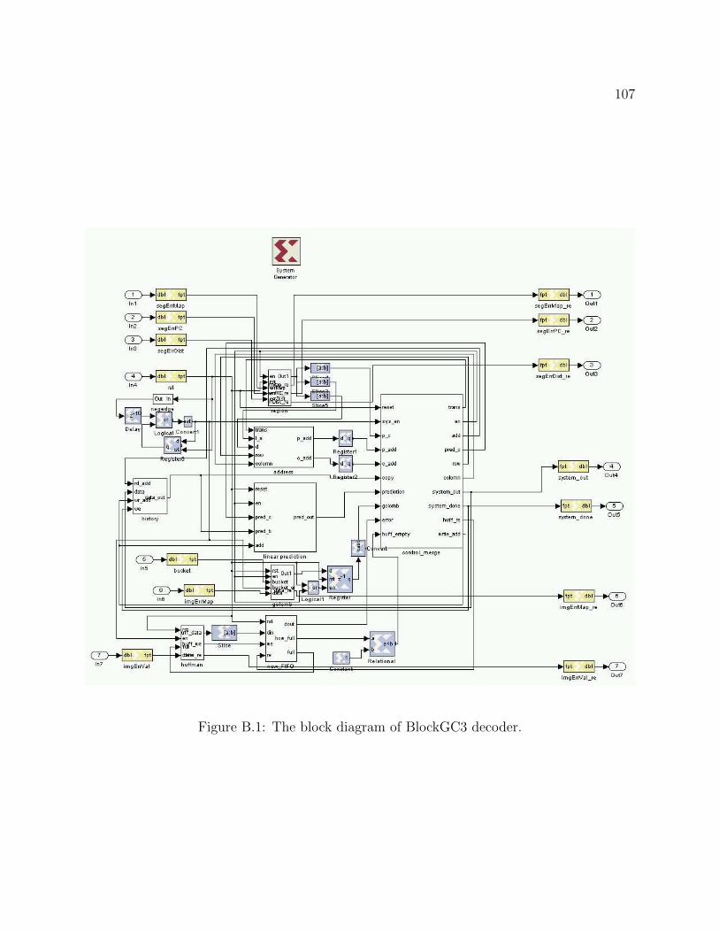
107
Figure B.1: The block diagram of BlockGC3 decoder.
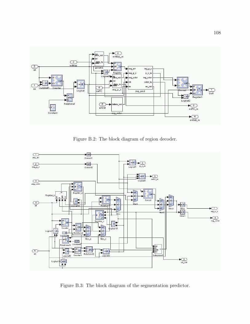
108
Figure B.2: The block diagram of region decoder.
Figure B.3: The block diagram of the segmentation predictor.
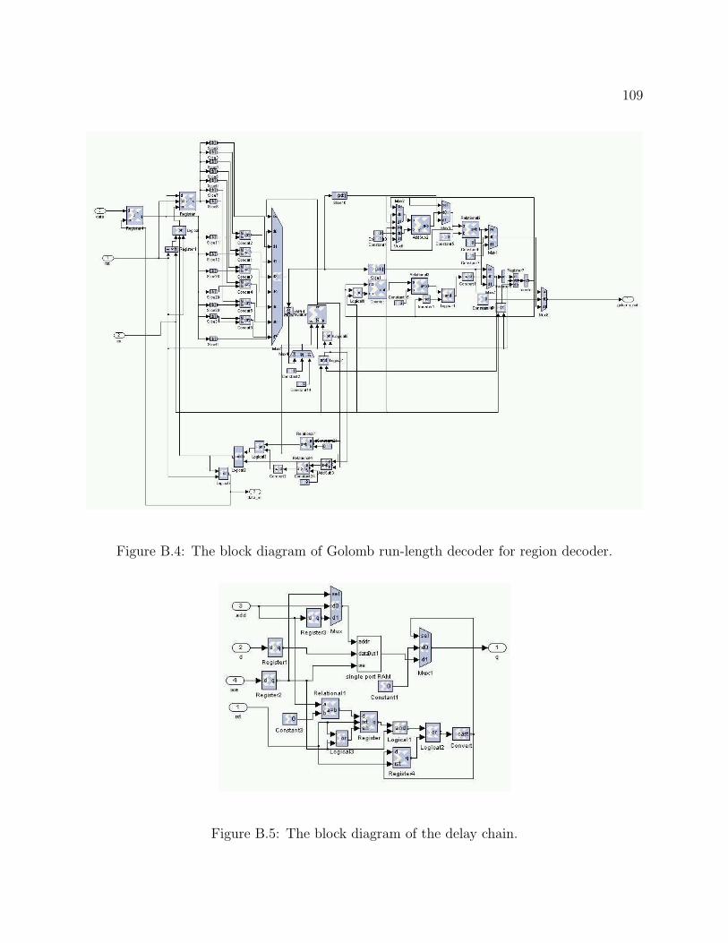
109
Figure B.4: The block diagram of Golomb run-length decoder for region decoder.
Figure B.5: The block diagram of the delay chain.
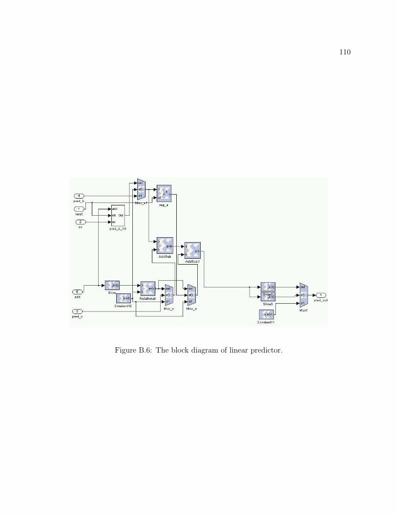
110
Figure B.6: The block diagram of linear predictor.
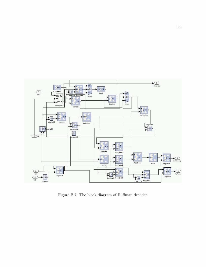
111
Figure B.7: The block diagram of Huffman decoder.
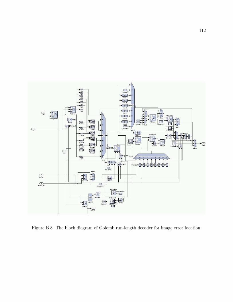
112
Figure B.8: The block diagram of Golomb run-length decoder for image error location.
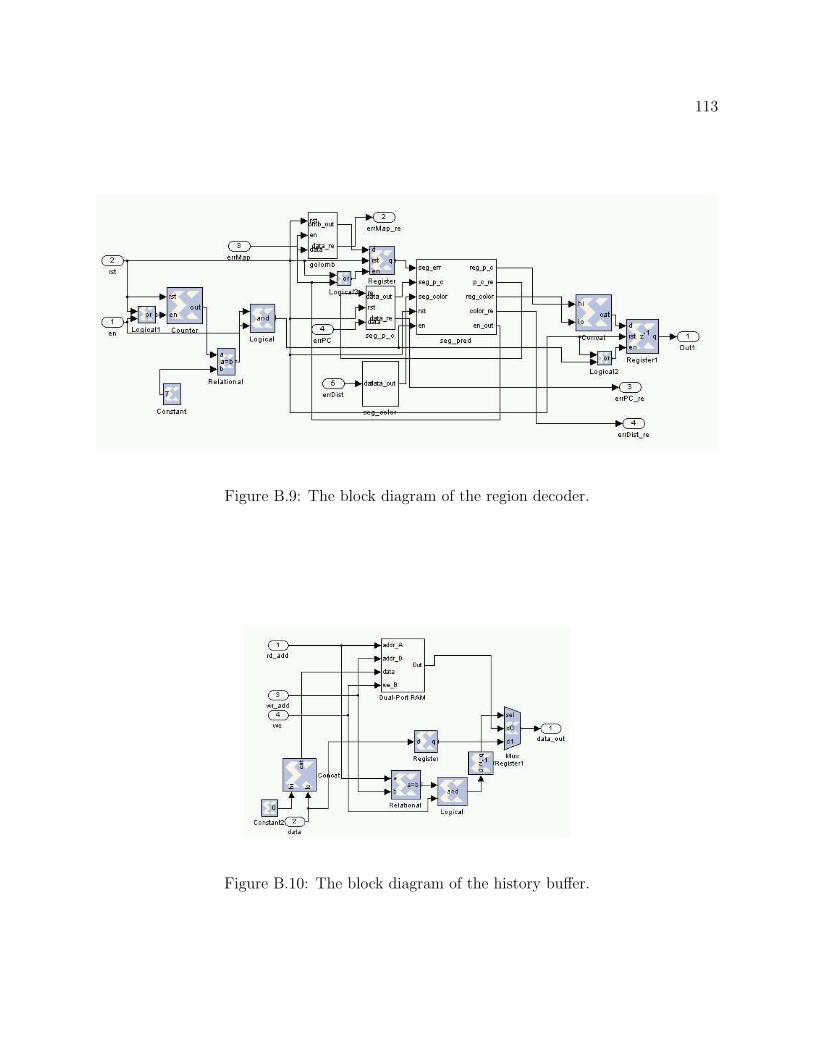
113
Figure B.9: The block diagram of the region decoder.
Figure B.10: The block diagram of the history buffer.
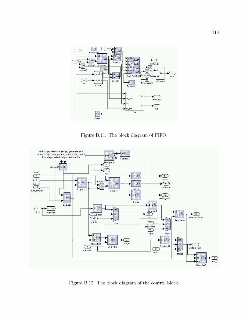
114
Figure B.11: The block diagram of FIFO.
Figure B.12: The block diagram of the control block.