arf leadership - asml leadership asml’s commitment to arf leadership continues with the newest...
TRANSCRIPT
EDITOR’S NOTE
Innovation leadership implies being out front
with new inventions, processes, or new ways of
working. As we enter the era of low k1, lithography
innovation leadership is needed more than ever
to extend the limits of optical lithography to high
volume manufacturing.
ASML has a proud history of l ithography
innovation leadership, ranging from the
introduction of Phase Grating Alignment in
1984 at the time of the company’s founding, to
our more recent revolutionary innovation, the
TWINSCAN platform, the industry’s fi rst and only
dual-stage lithography system.
The lead article in this issue of Images
showcases the TWINSCAN AT:1200B, a high NA
193-nm production tool, and the newest member
of the TWINSCAN family. This new system is
packed with innovations to enable high volume
manufacturing for 80 nm and beyond.
Another article in this issue describes
ASML’s integrated portfolio of products for en-
abling low k1 manufacturing—products like
LumenShaper, which allows customers to more
easily implement customized illumination to im-
prove their process latitude. And products like
LithoCruiser and MaskWeaver are described for
simultaneously optimizing scanner performance
and mask designs.
Two more articles on our Technology
Development Centers and Training Operations
describe innovative ways of working and
transferring knowledge, which ASML has
developed to enhance our customers’ ex-
perience and lithography productivity.
From steppers to scanners, innovation includes
the continuous evolution and improvement of our
platforms. This hallmark of ASML products’ value
of ownership is described in a pair of articles
on the “C” package productivity upgrades for
PAS 5500 and TWINSCAN, and the improved
imaging and overlay performance offered on the new
PAS 5500/350C.
Finally, it is important for you to know that at
ASML, our lithography innovations have always
been, and will continue to be, solely directed at
bringing more value to our customers’ lithography
operations.
Contents
4 ASML in the News
5-7 ASML ArF Leadership
Continues with
TWINSCAN AT:1200B;
a 0.85-NA Production Tool
for 80 nm Processing
8-11 Integrated Portfolio Enables
Low k1 Manufacturing
12-13 ASML’s Technology
Development Center –
Extending the Limits
for Customers
14-16 New TWINSCAN and
PAS 5500 Systems Increase
Productivity by up to 15%
18-19 ASML’s TWINSCAN
Training and Certifi cation
Program Sets Worldwide
Industry Standard in System
Performance and Support
20 ASML Extends its Portfolio
with 0.18-µm DUV Stepper
The LithographyInnovation Leaderby Mark Bigelow
IMAGES ASML’s CUSTOMER MAGAZINE
Editorial BoardDave Chavoustie
Paul van Attekum
Tom McGuire
Editor in ChiefMark Bigelow
Managing EditorRyan Young
Corporate EditorJane Mitchell
Contributing WritersNick Rowlands, Vivian Kim, Dorseda de Block,
Andrea Avery, Ryan Young
CirculationMichelle Herrick, Saskia Boeije, Emily Leung
© 2003, ASML.
ASML, ASM Lithography, TWINSCAN, PAS 5500, PAS 5000,
SA 5200, ATHENA, QUASAR, IRIS, FOCAL, CPL, DDL, Micralign,
Micrascan, 3DAlign, 2DStitching, 3DMetrology, MaskTools, LithoGuide,
MaskRigger, MaskWeaver, LithoCruiser, LumenShaper, Ultra-k1, Dose-
Mapper, SAMOS, ILIAS, and the ASML logo are trademarks of ASML
Holding N.V. or of affi liate companies. The trademarks may be used
either alone or in combination with a further product designation.
Starlith, AERIAL, and AERIAL II are trademarks of Carl Zeiss.
Nothing in this publication is intended to make representations with
regard to whether any trademark is registered or to suggest that any
sign other than those mentioned should not be considered to be a
trademark of ASML or of any third party.
ASML Images Summer 2003 3
IMAGINGTHE FUTUREIMAGINGTHE FUTURE
IT’S OUR COMMITMENT TO THE NEXT GENERATION
ASML produces the world’s most advanced lithography systems. Our technology
leadership enables IC makers to image today’s and tomorrow’s highest
performance chips.
ASML technology leadership is rooted in R&D and nourished by our people. We’re
committed to providing customers the right technology at the right time.
Technology leadership. It’s how we became the market leader. It’s how we’re
imaging the future. Find out more by visiting www.asml.com

4 ASML Images Summer 2003
ASML Maintains Momentum in China with Sale to ASMC
ASMC Selects ASML as “Tool of Choice” for New Facility
June 3, 2003 – ASML announced booking a multiple product order
from Advanced Semiconductor Manufacturing Corporation (ASMC),
a leading wafer foundry in Shanghai, China. The sale represents a
move forward in ASML’s bid to expand its position in the growing
Chinese chip market.
UMCi Chooses Advanced Lithography System from ASML
May 20, 2003 – ASML announced the sale of an advanced
lithography system to Singapore-based UMCi, a 300 nm foundry
joint venture company between UMC, Infineon Technologies and
Singapore’s Economic Development Board Investments (EDBI). At
full capacity, UMCi’s wafer foundry will produce up to 40,000 wafers
per month.
ASML Named World Leaderin Stepper Market
54 Percent Share of Market Captured by ASML
According to Analyst Firm
May 1, 2003 – ASML announced that the company has been named
the world leader in the semiconductor stepper market by Gartner
Dataquest, an independent research and consulting firm specializing
in the technology industry. The findings are based on market surveys
about 2002 revenues and unit sales from companies competing in the
capital equipment market.
ASML Secures Sale to Fuji Film Arch of Japan
Lithography System Selected to Support R&D
April 23, 2003 – ASML announced a sale in the Japanese market
to Fuji Film Arch (FFA), a major developer of photochemicals used in
semiconductor production. Japan is a market traditionally dominated
by local lithography suppliers.
ASML Delivers First Full-Field 157-nm Tool to IMEC
Other Customers Place Orders for 2003 Delivery
April 2, 2003 – ASML announced that it is delivering the industry’s
first full-field 157-nanometer step-and-scan tool to Europe’s leading
independent research and development chip consortium, Inter-
universities MicroElectronic Center (IMEC). Called the Micrascan VII,
the new system is the first 157-nm full-field tool able to create working
chips. IMEC will receive shipment in April 2003.
ASML and Samsung Sign Global IP Licensing Agreement
Patented Technology Enhances Imaging Performance
March 27, 2003 – ASML announced that Samsung Electronics Co.
Ltd. signed a licensing agreement for its Scattering Bar technology
to be deployed at Samsung’s semiconductor production facilities
worldwide. The patented ASML technology significantly enhances the
imaging performance for current and future technology generations.
Samsung is licensing the technology through the life of the patents.
ASML Receives Favorable Ruling from Full ITC
March 18, 2003 – ASML announced that the U.S. International
Trade Commission (ITC) in Washington D.C. ruled in favor of ASML on
all claims filed against the company by competitor Nikon Corporation
of Japan. The Commission denied the petition by Nikon seeking review
of the initial determination made by an administrative law judge on
January 29, 2003.
The Commission determined that ASML had not violated Section
337 of U.S. trade law, which governs investigations into allegations of
certain unfair practices in import trade.
Carl Zeiss Selects ASML MaskTools to Supply Advanced Lens Design Qualification Software
February 04, 2003 – ASML MaskTools announced that it has been
awarded a business contract by Carl Zeiss SMT AG to support the
design of high numerical aperture (NA) 193-nm and 157-nm lenses.
Lens quality and consistency are increasingly important factors as line
widths shrink to below half the wavelength of the exposure tool. ASML
MaskTools was engaged to develop a unique method and software
implementation for the lenses, improving layout cycle times while
maintaining design quality.
For complete information regarding these press announcements,
please refer to the press section of www.asml.com
ArF leadership
ASML’s commitment to ArF leadership continues
with the newest member of the proven dual-stage
TWINSCAN platform, the AT:1200B. This system
enables customers to achieve greater yield of more
sophisticated chips. The AT:1200B provides increased
productivity in high-volume manufacturing of 80-nm
applications. Equipped with ASML’s Ultra-k1 portfolio,
the AT:1200B meets the challenges of low-k1 manu-
facturing with subsystem improvements and new
functionality.
System Overview
The TWINSCAN AT:1200B 193-nm Step & Scan system is
a high-productivity, dual-stage, ArF lithography exposure tool
designed for high-volume production at 80-nm resolution. The
AT:1200B combines the imaging power of a variable (0.60–0.85)
Numerical Aperture (NA), Carl Zeiss Starlith 4X reduction lens with
AERIAL II illuminator technology.
Accelerating the Industry TowardLower k1 Applications
Dual wafer-stage technology provides maximum productivity
for both 300-mm and 200-mm applications, and enables
improvements to the focus and leveling operations to meet
stringent process control requirements. A 20-W ArF laser with
variable frequency control and a flexible, high-transmission
illuminator provide a production throughput of 103 wph (300 mm)
or 150 wph (200 mm), all at the lowest possible cost of operation.
New functionality on the AT:1200B includes flexible lens pupil
control, on-board measurement, and aerial image control from the
projection lens for the lowest possible aberrations, and minimi-
zation of stray light. This ensures performance for low k1 imaging.
Third Generation ArF Exposure Tool
ArF has become the technology of choice for leading edge
designs below 100 nm. The AT:1200B incorporates Carl Zeiss’
third generation ArF projection lens. This lens combines the high-
est NA and lowest number of aberrations of any ArF lens to date.
The system represents the latest addition to ASML’s well-estab-
lished ArF product range. The first shipments of ASML’s exposure
systems using 193-nm wavelength began in 1998 with the
PAS 5500/900 and later PAS 5500/950B. The PAS 5500/1100
and TWINSCAN AT:1100B were subsequently introduced in 2000
and 2001.
ASML ArF Leadership Continues with TWINSCAN AT:1200B, a 0.85-NA Production Tool for 80-nm Processingby Frank van de Mast & Alberto Pirati
0.6
0.5
0.7
0.4
0.8
0.3
0.9
80
Resolution (nm) = k1 x λ / NA
k 1 li
mit
100130150
PA
S 5
500/
950B
PA
S 5
500/
950B
AT:
1100
B, P
AS
550
0/11
00
0.85
0.35
AT
:120
0B
NA
k1
ASML in the News
ASML Images Summer 2003 5
6 ASML Images Summer 2003
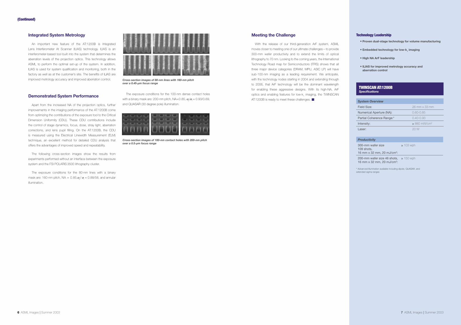
Integrated System Metrology
An important new feature of the AT:1200B is Integrated
Lens Interferometer At Scanner (ILIAS) technology. ILIAS is an
interferometer-based tool built into the system that determines the
aberration levels of the projection optics. This technology allows
ASML to perform the optimal set-up of the system. In addition,
ILIAS is used for system qualification and monitoring, both in the
factory as well as at the customer’s site. The benefits of ILIAS are
improved metrology accuracy and improved aberration control.
Demonstrated System Performance
Apart from the increased NA of the projection optics, further
improvements in the imaging performance of the AT:1200B come
from optimizing the contributions of the exposure tool to the Critical
Dimension Uniformity (CDU). These CDU contributions include
the control of stage dynamics, focus, dose, stray light, aberration
corrections, and lens pupil filling. On the AT:1200B, the CDU
is measured using the Electrical Linewidth Measurement (ELM)
technique, an excellent method for detailed CDU analysis that
offers the advantages of improved speed and repeatability.
The following cross-section images show the results from
experiments performed without an interface between the exposure
system and the FSI POLARIS 3500 lithography cluster.
The exposure conditions for the 80-nm lines with a binary
mask are: 160-nm pitch, NA = 0.85,σo/ σ
i = 0.88/58, and annular
illumination.
Cross-section images of 80-nm lines with 160-nm pitch over a 0.45-µm focus range
The exposure conditions for the 100-nm dense contact holes
with a binary mask are: 200-nm pitch, NA=0.85, σo/ σ
i = 0.93/0.69,
and QUASAR (30 degree pole) illumination.
Cross-section images of 100-nm contact holes with 200-nm pitch over a 0.5-µm focus range
(Continued)
Meeting the Challenge
With the release of our third-generation ArF system, ASML
moves closer to meeting one of our ultimate challenges—to provide
300-mm wafer productivity and to extend the limits of optical
lithography to 70 nm. Looking to the coming years, the International
Technology Road map for Semiconductors (ITRS) shows that all
three major device categories (DRAM, MPU, ASIC LP) will have
sub-100-nm imaging as a leading requirement. We anticipate,
with the technology nodes starting in 2004 and extending through
to 2006, that ArF technology will be the dominant wavelength
for enabling these aggressive designs. With its high-NA, ArF
optics and enabling features for low-k1 imaging, the TWINSCAN
AT:1200B is ready to meet these challenges.
Technology Leadership
• Proven dual-stage technology for volume manufacturing
• Embedded technology for low-k1 imaging
• High NA ArF leadership
• ILIAS for improved metrology accuracy and aberration control
System Overview
Field Size: 26 mm x 33 mm
Numerical Aperture (NA): 0.60-0.85
Partial Coherence Range:* 0.40-0.93
Intensity: ≥ 880 mW/cm2
Laser: 20 W
Productivity
300-mm wafer size 109 shots, 16 mm x 32 mm, 20 mJ/cm2:
≥ 103 wph
200-mm wafer size 46 shots, 16 mm x 32 mm, 20 mJ/cm2:
≥ 150 wph
* Advanced Illumination available including dipole, QUASAR, and extended sigma ranges
7 ASML Images Summer 2003
TWINSCAN AT:1200BSpecifications
low k1 manufacturing
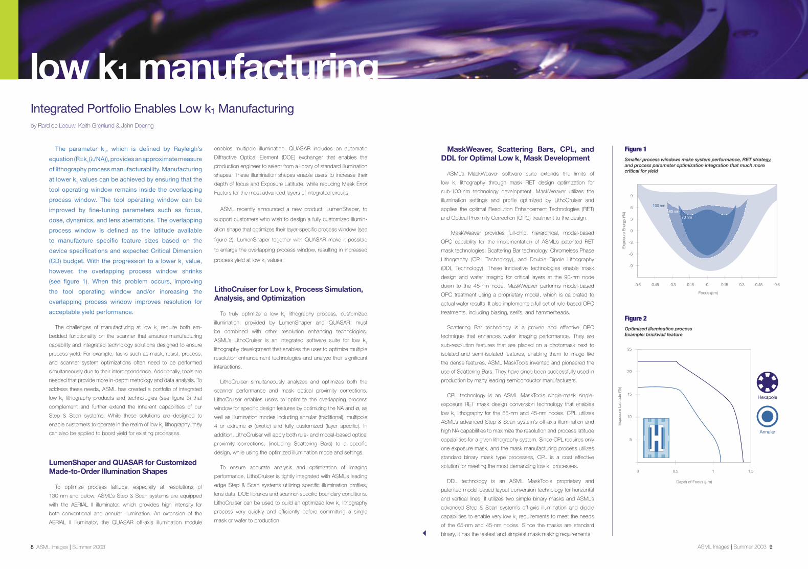
The parameter k1, which is defi ned by Rayleigh’s
equation (R=k1(λ/NA)), provides an approximate measure
of lithography process manufacturability. Manufacturing
at lower k1 values can be achieved by ensuring that the
tool operating window remains inside the overlapping
process window. The tool operating window can be
improved by fi ne-tuning parameters such as focus,
dose, dynamics, and lens aberrations. The overlapping
process window is defi ned as the latitude available
to manufacture specifi c feature sizes based on the
device specifi cations and expected Critical Dimension
(CD) budget. With the progression to a lower k1 value,
however, the overlapping process window shrinks
(see fi gure 1). When this problem occurs, improving
the tool operating window and/or increasing the
overlapping process window improves resolution for
acceptable yield performance.
The challenges of manufacturing at low k1 require both em-
bedded functionality on the scanner that ensures manufacturing
capability and integrated technology solutions designed to ensure
process yield. For example, tasks such as mask, resist, process,
and scanner system optimizations often need to be performed
simultaneously due to their interdependence. Additionally, tools are
needed that provide more in-depth metrology and data analysis. To
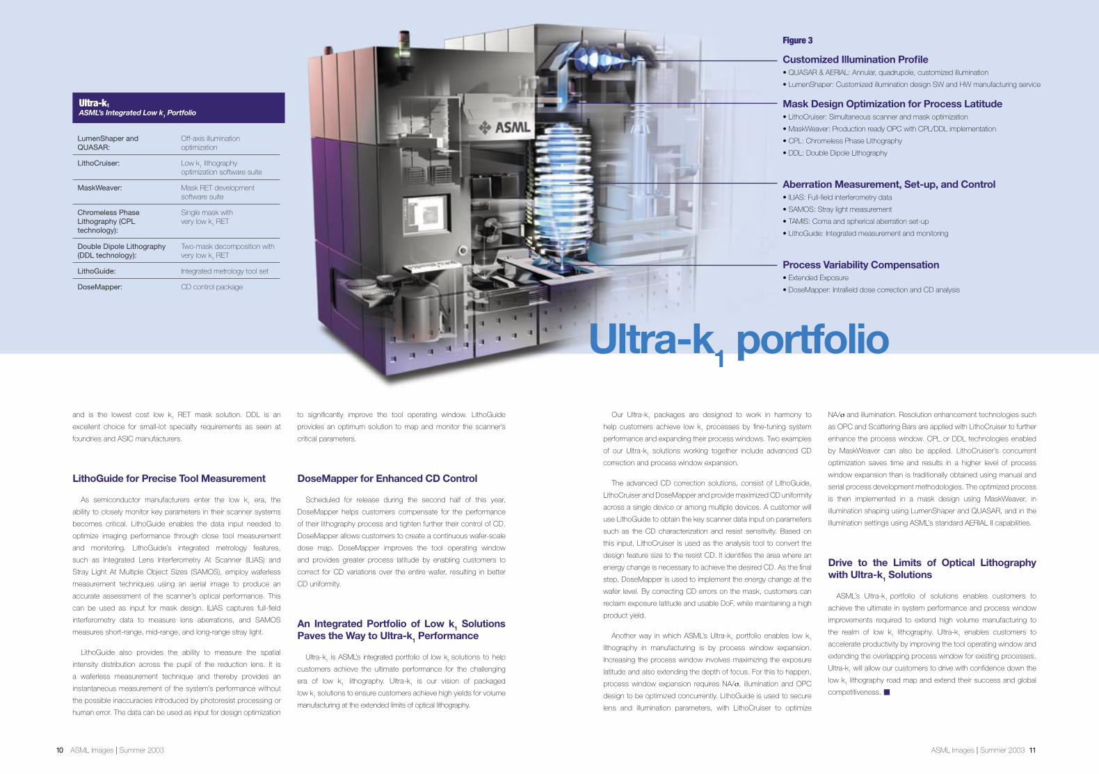
address these needs, ASML has created a portfolio of integrated
low k1 lithography products and technologies (see fi gure 3) that
complement and further extend the inherent capabilities of our
Step & Scan systems. While these solutions are designed to
enable customers to operate in the realm of low k1 lithography, they
can also be applied to boost yield for existing processes.
LumenShaper and QUASAR for Customized Made-to-Order Illumination Shapes
To optimize process latitude, especially at resolutions of
130 nm and below, ASML’s Step & Scan systems are equipped
with the AERIAL II illuminator, which provides high intensity for
both conventional and annular illumination. An extension of the
AERIAL II illuminator, the QUASAR off-axis illumination module
enables multipole illumination. QUASAR includes an automatic
Diffractive Optical Element (DOE) exchanger that enables the
production engineer to select from a library of standard illumination
shapes. These illumination shapes enable users to increase their
depth of focus and Exposure Latitude, while reducing Mask Error
Factors for the most advanced layers of integrated circuits.
ASML recently announced a new product, LumenShaper, to
support customers who wish to design a fully customized illumin-
ation shape that optimizes their layer-specifi c process window (see
fi gure 2). LumenShaper together with QUASAR make it possible
to enlarge the overlapping process window, resulting in increased
process yield at low k1 values.
LithoCruiser for Low k1 Process Simulation, Analysis, and Optimization
To truly optimize a low k1 lithography process, customized
illumination, provided by LumenShaper and QUASAR, must
be combined with other resolution enhancing technologies.
ASML’s LithoCruiser is an integrated software suite for low k1
lithography development that enables the user to optimize multiple
resolution enhancement technologies and analyze their signifi cant
interactions.
LithoCruiser simultaneously analyzes and optimizes both the
scanner performance and mask optical proximity corrections.
LithoCruiser enables users to optimize the overlapping process
window for specifi c design features by optimizing the NA and σ, as
well as illumination modes including annular (traditional), multipole
4 or extreme σ (exotic) and fully customized (layer specifi c). In
addition, LithoCruiser will apply both rule- and model-based optical
proximity corrections, (including Scattering Bars) to a specifi c
design, while using the optimized illumination mode and settings.
To ensure accurate analysis and optimization of imaging
performance, LithoCruiser is tightly integrated with ASML’s leading
edge Step & Scan systems utilizing specifi c illumination profi les,
lens data, DOE libraries and scanner-specifi c boundary conditions.
LithoCruiser can be used to build an optimized low k1 lithography
process very quickly and effi ciently before committing a single
mask or wafer to production.
Integrated Portfolio Enables Low k1 Manufacturingby Rard de Leeuw, Keith Gronlund & John Doering
8 ASML Images Summer 2003
MaskWeaver, Scattering Bars, CPL, and DDL for Optimal Low k1 Mask Development
ASML’s MaskWeaver software suite extends the limits of
low k1 lithography through mask RET design optimization for
sub-100-nm technology development. MaskWeaver utilizes the
illumination settings and profi le optimized by LithoCruiser and
applies the optimal Resolution Enhancement Technologies (RET)
and Optical Proximity Correction (OPC) treatment to the design.
MaskWeaver provides full-chip, hierarchical, model-based
OPC capability for the implementation of ASML’s patented RET
mask technologies: Scattering Bar technology, Chromeless Phase
Lithography (CPL Technology), and Double Dipole Lithography
(DDL Technology). These innovative technologies enable mask
design and wafer imaging for critical layers at the 90-nm node
down to the 45-nm node. MaskWeaver performs model-based
OPC treatment using a proprietary model, which is calibrated to
actual wafer results. It also implements a full set of rule-based OPC
treatments, including biasing, serifs, and hammerheads.
Scattering Bar technology is a proven and effective OPC
technique that enhances wafer imaging performance. They are
sub-resolution features that are placed on a photomask next to
isolated and semi-isolated features, enabling them to image like
the dense features. ASML MaskTools invented and pioneered the
use of Scattering Bars. They have since been successfully used in
production by many leading semiconductor manufacturers.
CPL technology is an ASML MaskTools single-mask single-
exposure RET mask design conversion technology that enables
low k1 lithography for the 65-nm and 45-nm nodes. CPL utilizes
ASML’s advanced Step & Scan system’s off-axis illumination and
high NA capabilities to maximize the resolution and process latitude
capabilities for a given lithography system. Since CPL requires only
one exposure mask, and the mask manufacturing process utilizes
standard binary mask type processes, CPL is a cost effective
solution for meeting the most demanding low k1 processes.
DDL technology is an ASML MaskTools proprietary and
patented model-based layout conversion technology for horizontal
and vertical lines. It utilizes two simple binary masks and ASML’s
advanced Step & Scan system’s off-axis illumination and dipole
capabilities to enable very low k1 requirements to meet the needs
of the 65-nm and 45-nm nodes. Since the masks are standard
binary, it has the fastest and simplest mask making requirements
Figure 1Smaller process windows make system performance, RET strategy, and process parameter optimization integration that much more critical for yield
Figure 2Optimized illumination processExample: brickwall feature
�
��
�
��
�
��
�
� ����
����� ����
���
����
��
����
���
�
����� ������� ������� ���������
�� ���� ��
��� ��
ASML Images Summer 2003 9
��
��
��
�
��
���
����� �� ����� ����
���
�������
�����
���
�
�����
�������
��������
Our Ultra-k1 packages are designed to work in harmony to
help customers achieve low k1 processes by fine-tuning system
performance and expanding their process windows. Two examples
of our Ultra-k1 solutions working together include advanced CD
correction and process window expansion.
The advanced CD correction solutions, consist of LithoGuide,
LithoCruiser and DoseMapper and provide maximized CD uniformity
across a single device or among multiple devices. A customer will
use LithoGuide to obtain the key scanner data input on parameters
such as the CD characterization and resist sensitivity. Based on
this input, LithoCruiser is used as the analysis tool to convert the
design feature size to the resist CD. It identifies the area where an
energy change is necessary to achieve the desired CD. As the final
step, DoseMapper is used to implement the energy change at the
wafer level. By correcting CD errors on the mask, customers can
reclaim exposure latitude and usable DoF, while maintaining a high
product yield.
Another way in which ASML’s Ultra-k1 portfolio enables low k
1
lithography in manufacturing is by process window expansion.
Increasing the process window involves maximizing the exposure
latitude and also extending the depth of focus. For this to happen,
process window expansion requires NA/σ, illumination and OPC
design to be optimized concurrently. LithoGuide is used to secure
lens and illumination parameters, with LithoCruiser to optimize
NA/σ and illumination. Resolution enhancement technologies such
as OPC and Scattering Bars are applied with LithoCruiser to further
enhance the process window. CPL or DDL technologies enabled
by MaskWeaver can also be applied. LithoCruiser’s concurrent
optimization saves time and results in a higher level of process
window expansion than is traditionally obtained using manual and
serial process development methodologies. The optimized process
is then implemented in a mask design using MaskWeaver, in
illumination shaping using LumenShaper and QUASAR, and in the
illumination settings using ASML’s standard AERIAL II capabilities.
Drive to the Limits of Optical Lithography with Ultra-k1 Solutions
ASML’s Ultra-k1
portfolio of solutions enables customers to
achieve the ultimate in system performance and process window
improvements required to extend high volume manufacturing to
the realm of low k1 lithography. Ultra-k
1 enables customers to
accelerate productivity by improving the tool operating window and
extending the overlapping process window for existing processes.
Ultra-k1 will allow our customers to drive with confidence down the
low k1 lithography road map and extend their success and global
competitiveness.
and is the lowest cost low k1 RET mask solution. DDL is an
excellent choice for small-lot specialty requirements as seen at
foundries and ASIC manufacturers.
LithoGuide for Precise Tool Measurement
As semiconductor manufacturers enter the low k1 era, the
ability to closely monitor key parameters in their scanner systems
becomes critical. LithoGuide enables the data input needed to
optimize imaging performance through close tool measurement
and monitoring. LithoGuide’s integrated metrology features,
such as Integrated Lens Interferometry At Scanner (ILIAS) and
Stray Light At Multiple Object Sizes (SAMOS), employ waferless
measurement techniques using an aerial image to produce an
accurate assessment of the scanner’s optical performance. This
can be used as input for mask design. ILIAS captures full-field
interferometry data to measure lens aberrations, and SAMOS
measures short-range, mid-range, and long-range stray light.
LithoGuide also provides the ability to measure the spatial
intensity distribution across the pupil of the reduction lens. It is
a waferless measurement technique and thereby provides an
instantaneous measurement of the system’s performance without
the possible inaccuracies introduced by photoresist processing or
human error. The data can be used as input for design optimization
to significantly improve the tool operating window. LithoGuide
provides an optimum solution to map and monitor the scanner’s
critical parameters.
DoseMapper for Enhanced CD Control
Scheduled for release during the second half of this year,
DoseMapper helps customers compensate for the performance
of their lithography process and tighten further their control of CD.
DoseMapper allows customers to create a continuous wafer-scale
dose map. DoseMapper improves the tool operating window
and provides greater process latitude by enabling customers to
correct for CD variations over the entire wafer, resulting in better
CD uniformity.
An Integrated Portfolio of Low k1 Solutions Paves the Way to Ultra-k1 Performance
Ultra-k1 is ASML’s integrated portfolio of low k
1 solutions to help
customers achieve the ultimate performance for the challenging
era of low k1 lithography. Ultra-k
1 is our vision of packaged
low k1 solutions to ensure customers achieve high yields for volume
manufacturing at the extended limits of optical lithography.
Figure 3
Ultra-k1 portfolio
Customized Illumination Profile• QUASAR & AERIAL: Annular, quadrupole, customized illumination
• LumenShaper: Customized illumination design SW and HW manufacturing service
Mask Design Optimization for Process Latitude• LithoCruiser: Simultaneous scanner and mask optimization
• MaskWeaver: Production ready OPC with CPL/DDL implementation
• CPL: Chromeless Phase Lithography
• DDL: Double Dipole Lithography
Aberration Measurement, Set-up, and Control• ILIAS: Full-field interferometry data
• SAMOS: Stray light measurement
• TAMIS: Coma and spherical aberration set-up
• LithoGuide: Integrated measurement and monitoring
Process Variability Compensation• Extended Exposure
• DoseMapper: Intrafield dose correction and CD analysis
LumenShaper and QUASAR:
Off-axis illumination optimization
LithoCruiser: Low k1 lithography
optimization software suite
MaskWeaver: Mask RET development software suite
Chromeless Phase Lithography (CPL technology):
Single mask with very low k
1 RET
Double Dipole Lithography (DDL technology):
Two-mask decomposition with very low k
1 RET
LithoGuide: Integrated metrology tool set
DoseMapper: CD control package
Ultra-k1ASML’s Integrated Low k1 Portfolio
10 ASML Images Summer 2003 ASML Images Summer 2003 11
TDC scientists work closely with customers to facilitate Joint
Development Projects (JDPs). In cooperation with account
managers at the customer site and development engineers, JDPs
are initiated to develop new products or to drive tool performance
to improve the customer’s product. JDPs enable our customers to
refine their design processes to more closely match our system
capabilities. Doing so enables customers to make better products
using our systems. The work done in these projects also offers
ASML great insight into how our customers use ASML equipment,
what type of problems arise, how to solve them, and how to
best match ASML’s systems to our customers’ needs. From the
continuous and significant data collected, ASML receives early
insight to formulate accurate long-term product and technology
road maps that better meet market needs. This work is executed
in cooperation with our customer support and equipment
engineers to ensure proper implementation of the results received
from the JDPs.
TDC also engages with partner/supplier companies who
support different parts of the lithography process such as masks,
photoresists, optics, and lasers to determine more accurately
when, how, and to what extent we are able to enhance our
technology and imaging capabilities.
“TDC was initiated to add value to our customers. Working with
customers to solve low k1 imaging, 193-nm and 157-nm issues
enhances the customer’s process and production as well as
provides insight into future requirements,” concludes Arnold. By
working closely with other ASML engineers in Veldhoven, Wilton,
and ASML MaskTools, the TDC is helping refine tool use today and
define products for tomorrow.
process expertise
Extending the traditional limits of optical lithography
is an increasingly common requirement from our cus-
tomers. ASML’s Technology Development Center (TDC)
is committed both to enabling efficient utilization of
ASML tools to meet advanced customers’ process
requirements and to understanding their long term
technology needs. In close collaboration with
Development Engineering and MaskTools, TDC works
intensively with customers to establish high yielding
processes, as well as higher value IC products through
effective use of our innovative technology.
A New Era in Technology Creates the Need for ASML’s TDC
To meet the needs of the continued shrink in critical dimensions
below the half illumination wavelength, the technological
complexity of lithography tools has increased significantly. This
has created a new era of scientific challenges such as lower k1
values and decreased process tolerances. As a result, there is
a need to provide customers with advanced process-related
technical support to get the maximum value from their new tool,
while meeting the market demands at the right time.
“It was logical that our customers expected more from us, the
makers of the tool, and to give them the best advice on how to
improve performance through specific tool applications. In the past,
Technology, Development, and Customer Support departments
collaborated to support the customer. However, with the ever-
growing advances in technology, it became evident that to ensure
our customers’ success with our tools, even more dedicated time
to them was required by personnel closely located to the fab
manager and sites,” remarks Martin van den Brink, Executive Vice
President of Marketing & Technology.
It was with this objective in mind that ASML created TDC. TDC
intensifies ASML’s expertise in the areas of imaging, optics, reticles,
process integration and photoresist technology. “This added
expertise working in concert with account teams, development and
customer support resources enables customers to quickly adopt
new tools and technologies that bring them to full manufacturing
capacity in a timely manner,” emphasizes Bill Arnold, Chief Scientist
and Vice President of the Technology Development Center.
The TDC was established in the United States in 1999
and today is composed of leading senior lithography scientists
with strong academic backgrounds, expertise in research and
development, and extensive work experience as both a customer
and a vendor in a fab environment. “Customers benefit from a
dialogue with ASML staff who understand their current and future
technology requirements from a high volume production fab
perspective,” comments Mircea Dusa, a TDC scientist and ASML
Fellow specializing in lithography process integration.
In 2001, a TDC was also established in Hsin-chu, Taiwan to
serve customers throughout Asia. This group operates under the
leadership of Alek Chen, Senior Imaging Scientist and Director of
TDC, Asia.
Extending the Tool’s Imaging Performance
TDC specializes in understanding our customers’ advanced
technology needs while optimizing the imaging performance of
the existing installed base of advanced products in the following
areas:
• Customized illumination for specific layer designs
• Optimal mask choice and enhancements
• Resist process improvements
• Resolution of materials/manufacturing process integration issues
• Ultra high NA optics applications
• Simulation of new imaging techniques and tools
• Advanced technologies in focus and overlay
ASML’s Technology Development Center –Extending the Limits for Customersby Bill Arnold & Kevin Cummings
Customer Focus
• TDC is focused on enabling efficient utilization of existing leading-edge ASML tools in their fabs and understanding our customers’ long-term technology requirements
• Joint Development Projects (JDPs) enable customers to refine design processes to more closely match system capabilities
• As part of ASML’s matrixed organization, TDC provides process expertise to support advanced customers
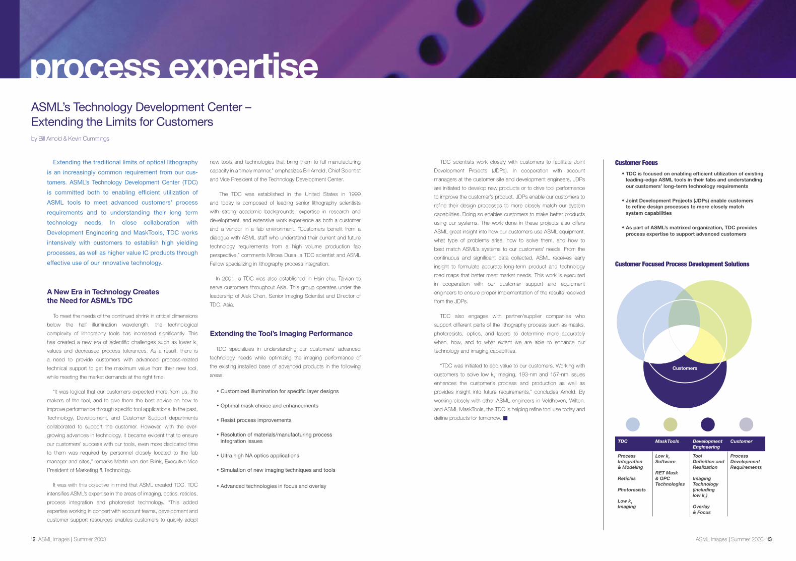
Customer Focused Process Development Solutions
TDC MaskTools Development Engineering
Customer
Process Integration & Modeling
Reticles
Photoresists
Low k1 Imaging
Low k1 Software
RET Mask & OPC Technologies
Tool Definition and Realization
Imaging Technology (including low k1)
Overlay & Focus
ProcessDevelopment Requirements
Customers
12 ASML Images Summer 2003 ASML Images Summer 2003 13

ASML Images Summer 2003 15
PAS 5500 Product Overview
The PAS 5500/1150C 193-nm Step & Scan system enables
90-nm mass production. This system, the industry’s leading
resolution tool, stretches the current technology to its limit. The
PAS 5500/1150C combines the proven imaging power of the
0.75 NA four-times-reduction lens with AERIAL II illumination
technology. An array of optional, advanced illumination-
enhancement technologies is available for this system. The
system is equipped with ATHENA and reticle blue align,
providing an increased accuracy of single machine overlay of
less than 12 nm. The 8-Spot Level Sensor improves focus and
leveling, particularly for edge dies, for better process control.
Highly line-narrowed 20-W ArF lasers with variable frequency
control, in combination with the high optical transmission of
the complete system, provide a production throughput of
135 wph for 200-mm wafers.
The introduction of the PAS 5500/850C DUV Step & Scan
system for 110-nm mass production stems from continuous
improvements to the industry’s highest-NA optical system, the
PAS 5500/850. The optional high-sigma DOE that is available
for this system can even extend the production resolution of the
PAS 5500/850C to 100 nm. Combining the imaging power of
a 0.80 NA four-times-reduction lens with AERIAL II illumination
technology, this system offers unprecedented imaging power
flexibility. Like the PAS 5500/1150C, ATHENA and reticle blue
align provide single machine overlay accuracy, which on the
PAS 5500/850C is less than 15 nm. A 320-mm/sec high-
speed wafer stage, in combination with highly line-narrowed
20-W KrF lasers and the high optical transmission of the
system, provides a production throughput of 135 wph for
200-mm wafers.
PAS 5500/1150C 90-nm dense lines performance. A binary mask was used, and the illumination conditions were as follows: NA= 0.75, and sigma 0.89/0.65.
-0.30 µm -0.25 µm -0.20 µm -0.15 µm -0.10 µm -0.05 µm 0.0 µm
0.05 µm 0.10 µm 0.15 µm 0.20 µm 0.25 µm 0.30 µm
increased productivity
ASML has developed performance enhancements
for its TWINSCAN and PAS 5500 lithography systems.
Called TWINSCAN C and PAS 5500 C, the new
enhancements increase wafer output for 300-mm and
200-mm wafers, at real production conditions, while
improving imaging, alignment, and leveling accuracy.
Realization of these productivity improvements is due mainly
to the increased stage speeds in these platforms. However,
other enhancements on these systems include unprecedented
imaging power and process control that drive production reso-
lution on ArF systems down to 90 nm and on KrF systems down
to 100 nm.
The TWINSCAN C product enhancements will be available
on four systems: the AT:400C, AT:750C, AT:850C, and
AT:1150C. The PAS 5500 C product enhancements are found in the
PAS 5500/850C and PAS 5500/1150C. These new systems
began shipping in the second quarter of 2003.
Optimized Imaging with AERIAL II Illumination Technology—Reduction of k1 Without Intensity or Throughput Loss
A common element in both the TWINSCAN and PAS 5500
systems is AERIAL II illumination technology. This technology
enables continuous, variable, conventional illumination, and off-
axis illumination with zoom optics for maintaining high throughput.
There are a number of optional modules available for the new
TWINSCAN C and PAS 5500 C systems. These optional modules
include the QUASAR Multipole Illumination Module—a software-
controlled automatic Diffractive Optical Element (DOE) exchanger
that maximizes the flexibility of the AERIAL II illuminator—and a high
sigma DOE, used in combination with QUASAR that extends the
sigma range.
DOEs, whether standard, or customized through LumenShaper,
work in concert with the full pupil-shaping flexibility of the AERIAL II
illuminator and the QUASAR off-axis illumination module to generate
the optimum pupil shape in the imaging tool, while maintaining high
illumination intensity.
This use of DOE technology allows customers to fine tune the
imaging of their system to meet their specific purposes, while
improving imaging performance at low k1. This optimization of the
illumination can bring substantial improvements to the process
window.
A software-controlled automatic DOE exchanger maximizes the flexibility of the AERIAL II illuminator. The DOE shapes shown, from top left to bottom right, are: conventional, low sigma, annular, high sigma, QUASAR, cQuad, dipole 35° (X), and dipole 90° (Y).
Value of Ownership
• I-Line, KrF and ArF production improvements of up to 15%
• Production resolutions of 90 nm for ArF systems, and 100 nm for KrF systems
• LumenShaper and QUASAR: Off-axis illumination optimization
• Improved focus and leveling for better process control
New TWINSCAN and PAS 5500 SystemsIncrease Productivity by up to 15%by Ron Kool & Rob van Keulen
14 ASML Images Summer 2003

TWINSCAN Product Overview
The TWINSCAN AT:1150C 193-nm Step & Scan system is a high-
productivity, dual-stage, ArF lithography tool designed for volume 300-
mm wafer production at 90-nm resolution. The AT:1150C combines
the imaging power of a variable (0.50–0.75) Numerical Aperture (NA),
Carl Zeiss Starlith, four-times-reduction lens with AERIAL II illuminator
technology. The level sensor improves focus and leveling, particularly
on edge dies, for better process control. A 20-W ArF laser with variable
frequency control, in combination with the high optical transmission of
the complete system, provides a production throughput of 107 wph
for 300-mm wafers.
The TWINSCAN AT:850C is a 248-nm KrF system capable of
volume 300-mm wafer production at a resolution of 110 nm and
below. The imaging power of this system comes from a variable
(0.55–0.80) NA, Starlith, four-times-reduction lens in combination with
AERIAL II and QUASAR illuminator technology. The AT:850C extends
ASML’s proven KrF technology to 100-nm applications, and next
generation chip design rules can exploit the improved overlay from
ATHENA. Furthermore, innovative off-axis wafer mapping improves
the focus and leveling capabilities of this system. Highly line-narrowed
20-W KrF lasers with variable frequency control, in combination
with the high optical transmission of the optical system, provide
a production throughput of 112 wph for 300-mm wafers. A high
power, 30-W laser is available as a factory option.
The TWINSCAN AT:750C continues the trend of high-productivity
made possible by dual-stage technology. This 248-nm KrF Step &
Scan system drives production resolutions on 300-mm wafers down
to 130 nm. The combination of the variable (0.50–0.70) NA lens with
AERIAL II illuminator technology again offers powerful imaging. The
level sensor improves focus and leveling, particularly on edge dies,
for better process control. Highly line-narrowed 20-W KrF lasers
with variable frequency control, in combination with the high optical
transmission of the optical system, provide a production throughput
of 112 wph for 300-mm wafers.
A 365-nm Step & Scan system, the TWINSCAN AT:400C,
completes the enhanced TWINSCAN C product range. This
high-productivity, dual-stage system offers volume 300-mm wafer
production at a resolution of 280 nm. A high power 5-kW Hg lamp
and fast stages ensure maximum productivity by minimizing the
exposure scanning time per field and the stepping time between
fields. The level sensor in combination with the TWINSCAN leveling
approach virtually eliminates differences between inner dies and
edge dies and ensures a high yield across the entire wafer. Further
enhancements on this system include fast reticle exchange times
and lot streaming.
TWINSCAN AT:850C 90-nm dense lines (pitch 1:1) performance. A binary mask was used, and the illumination conditions were as follows: cQuad illumination, NA = 0.8, and sigma 0.9/0.72.
-0.50 µm -0.45 µm -0.40 µm -0.35 µm -0.30 µm -0.25 µm -0.20 µm
90.6 nm 87.9 nm 92.1 nm 92.5 nm 91.2 nm 94.2 nm 94.4 nm
-0.15 µm -0.10 µm -0.05 µm 0.0 µm +0.05 µm +0.10 µm +0.15 µm
92.9 nm 90.2 nm 92.7 nm 92.5 nm 89.7 nm 88.7 nm 81.1 nm
16 ASML Images Summer 2003
ASML is committed to technology leadership. ASML TWINSCAN™ lithography
systems deliver the highest productivity at the limits of optical lithography.
TWINSCAN is the only platform that combines world-class measurement accuracy
with simultaneous, nonstop wafer imaging because it’s the only system with dual stages.
Why have the world’s leaders in 300 mm productivity chosen TWINSCAN?
Dual stages. Race them for yourself on our test track at www.asml.com/dualstages.
THE WORLD’S ONLY DUAL-STAGE LITHOGRAPHY SYSTEM
RACE AHEAD WITHTWINSCANRACE AHEAD WITHTWINSCAN

training & certification
Even as semiconductor technology continues to
become increasingly sophisticated, ASML maintains its
position as the world’s leading supplier of lithographic
imaging solutions. Contributing significantly to this
status is ASML’s demonstrated dedication to optimal
system performance and use. Through commitment
to customer satisfaction, ASML has developed the
industry-leading TWINSCAN Training and Certification
Program, aimed at ensuring that every TWINSCAN
service engineer worldwide has the same high level of
proficiency and expertise.
“Our customers deserve more than just leading-edge tech-
nology,” says Jerry Holtzclaw, U.S. Training Manager. “They also
deserve the security of knowing that their engineers have the skills
required to optimize system performance and use.”
Courses to Suit Every Engineer at Every Level
The wide variety of training programs offered—ranging from self-
paced multimedia courses incorporating e-learning to intensive,
hands-on practical training—ensures that both customer engineers
and ASML engineers have those skills so crucial to system support.
Graham Murray, Director Worldwide Training, explains how ASML’s
performance-based Training and Certification Program provides
variable paths to certification based on the demonstrated abilities
of the engineer. “We provide four distinct training paths to suit an
individual engineer’s experience,” Murray says. “This ensures that,
whatever the program entry point, certification is achieved to the
same high standard.” (See figure 1.)
The courses offered as a part of the TWINSCAN Training and
Certification Program follow a logical progression, thoroughly
covering material in each level before advancing to the next.
For example, the Level 1 System Introduction Course, which
is the initial course for all engineers, technicians, and operators
assigned to any TWINSCAN support capacity, provides students
with a basic introduction to the machine operation and an
in-depth explanation of each subsystem. This course is available
in both traditional and multimedia formats. In addition to this
Level 1 Course, the Level 1 Introduction and Operations Course
is a course designed specifically for on-site delivery to customer
TWINSCAN Operators and Technicians, and thoroughly covers
machine operations and safety.
Figure 1
Wk. Path 4
New Hire
Path 3
Lithography Experienced
Path 2
Experienced 5500 Engineers
Path 1
Experienced TWINSCAN Engineers
1
2
3
4
5
6
7
8
9
10
11
12
13
14
15
16
17
18
19
20
21
22
23
24
25
26
ASML’s TWINSCAN Training and Certification Program Sets Worldwide Industry Standard in System Performance and Support
Hands-on Instruction at Worldwide Training Facilities
The Level 2 course, Preventative Maintenance, addresses the
needs of maintenance engineers and technicians. The focus is
on hands-on, performance-based training and experience. During
this two-week course, students spend eighty percent of their
time in profitable hands-on learning, performing preventative
maintenance tasks on dedicated training equipment. This course
is also available to customers on-site, upon request. The six-week
Level 3 course, which covers maintenance adjustments, repair and
replacement, and general diagnostics, is targeted to maintenance
engineers and technicians. Participants receive extensive hands-on
practical exposure, performing advanced maintenance procedures
and calibrations, running software, replacing spare parts, and
mastering machine set-up sequences and system diagnostics.
(See figure 2.)
ASML’s customer commitment is evident in every aspect of
training. Training takes place in ASML’s four training centers, all
of which provide students with the opportunity to work hands-
on with full-scale, leading-edge ASML systems in a faithful fab
environment, fully preparing engineers for all aspects of system
support in the field. Each one of these established, dedicated
facilities, unmatched by any training centers in the industry, is
entirely equipped with state-of-the-art systems, and all courses are
delivered by experienced, certified technical instructors. As much
as eighty percent of the course content consists of unique hands-
on learning, often considered the most beneficial learning method
available. Hands-on experience, combined with the unparalleled
facilities, and the fact that class sizes are limited, guarantees each
student maximum system exposure and value from the training
experience.
Training is typically delivered in English, or in the local language
at each of ASML’s training centers, while on-site training courses
are delivered in the customer’s local language. Whether training is
taking place at the training center in the Netherlands, Taiwan, Korea,
or the U.S., Murray points out that “ASML’s Worldwide Training
Organization has a highly flexible team that can always overcome
any barriers language brings to the learning environment.”
Customer Focus
• Wide range of training options: - Virtual classroom e-learning - Interactive multimedia computer based training - Hands-on practical training
• Performance based instruction
• Full-scale systems in a fab environment
• Regional Facilities: The Netherlands, Taiwan, Korea, United States
Figure 2
Level Description Length
Level 0 (L0) Prerequisite Training, Orientation, Safety, Contamination
Level 1 (L1) Computer Based Training
System Introduction Self-paced
Level 1* (L1) Customer Introduction and Operations
2 days
Level 2 (L2) Preventitive Maintenance 2 weeks
Level 3 (L3) General Diagnostics, Layout, Airmounts, Sensors
Wafer and Reticle Handler
Wafer and Reticle Stage
Illumination and Projection
Advanced Alignment
Metrology
1 week
1 week
1 week
1 week
1 week
1 week
Validation Skill Certification in the Field
*L1 Introduction and Operations for customers only
Available Courses
Level 0 Level 2 Validation
Level 1 Level 3
ASML Images Summer 2003 19 18 ASML Images Summer 2003

3DAlign™, an optical front-to-back alignment technology, allows ASML’s
production-proven lithography steppers to provide fully automated,
high-throughput, double-sided processing of MEMS devices.
The 3DAlign option also enables high accuracy, back-to-back and mixed front/back
alignment for power, discrete and compound chip manufacturers.
This capability solves process-induced challenges such as CMP lapped
marks, epi shift for thick epi layers and noisy signals from grainy metal.
ASML’s commitment to special applications solutions is making the
world’s best ideas fly. See 3DAlign in action at www.asml.com/3DAlign.
extended portfolio
The new PAS 5500/350C stepper system, the
successor to the PAS 5500/300, is good news for
users seeking resolution and image improvements over
former stepper capabilities. The PAS 5500/350C is a
Deep UltraViolet (DUV) stepper for 0.18-µm applications
and beyond. The /350C’s 10-W KrF laser and AERIAL
illuminator enable high productivity for all applications.
The new system also provides an ideal mix-and-match
solution for i-line stepper fabs seeking to advance their
process capabilities.
DUV Stepper Enables Process Advances
The most advanced lithography processes employ DUV step-
and-scan systems. However, DUV steppers continue to fill an
important role in more mature fabs that wish to advance from i-line
to DUV. For example, many silicon and compound IC applications
that, until now, have used i-line steppers are migrating to processes
or technology nodes that require DUV imaging. While their
resolution requirements are moving into DUV territory, they still want
to continue to use their existing i-line steppers for the less critical
layers. For these users, the PAS 5500/350C provides DUV imaging
that is much more cost efficient than the more complex and more
expensive step-and-scan technology. Because it operates well in
mixed i-line and DUV stepper environments, the /350C provides
these users with an optimum mix-and-match solution.
Significant Resolution and Overlay Improvements
While the /350C delivers the same high throughput as the
/300C, the new stepper offers significant imaging and overlay
improvements over the /300C. The imaging improvements were
achieved by optimizing the adjustment of the lens, resulting in
better lens performance. In addition, the /350C’s improved critical
dimension (CD) performance results in resolution improvements
from 0.25 µm in the /300C down to 0.18 µm and beyond in
the /350C.
Along with the enhanced resolution of the new stepper comes
an improvement in the overlay performance. While an Improved
Overlay for Stepper (IOSt) package was an option for the /300,
it is now a standard feature of the /350C. The IOSt package is
a phase-modulated alignment system, which greatly enhances
overlay. Without the IOSt option, the /300 produced an overlay of
45 nm, versus the impressive 25 nm delivered by the /350C.
Enabling 0.18-µm technology in high-volume production, the
PAS 5500/350C fills an ever-increasing need as customers extend
their stepper infrastructure to DUV technology.
Value of Ownership
• Presents an important next step in the imaging improvement road map for /300 customers
• Shrinks CD to 0.18 µm and beyond
• Offers a significant overlay improvement
• Provides an ideal mix-and-match i-line stepper solution
ASML Extends its Portfolio with 0.18-µm DUV Stepperby Markus Hankeln
PAS 5500/350CKey Specifications
Lens
Numerical Aperture (NA): Variable 0.40-0.63
Resolution: ≤ 0.18 µm
Field Size
X & Y: 22 x 22 mm
Overlay
Two-point Global Alignment: ≤ 25 nm
Throughput
200-mm wafers, 70 shots, 30 mJ/cm2:
≥ 88 wph
20 ASML Images Summer 2003
WHEN ALIGNMENT IS CRITICAL TO PERFORMANCE
FLY WITH ASML
3DAlignFLY WITH ASML
3DAlign