arhitectura sistemelor de calcul 34. sisteme bazate pe...
TRANSCRIPT
Platformă de e-learning și curriculă e-content pentru învățământul superior tehnic
Arhitectura Sistemelor de Calcul
34. Sisteme bazate pe Cells

2
Motivation

3
Motivation: Cell Goals
• Outstanding performance, especially on game/multimedia applications.
– Challenges: Memory Wall, Power Wall, Frequency Wall
• Real time responsiveness to the user and the network.
– Challenges: Real-time in an SMP environment, Security
• Applicable to a wide range of platforms. – Challenge: Maintain programmability while increasing
performance
• Support an introduction in 2005/6. – Challenge: Structure innovation such that 5yr. schedule can
be met

4
Computing Paradigm Shift Today:
– Single thread performance hitting limits • Architecture and process technology saturated • Small percentage gains expected to remain
But: – Signs of paradigm shift to application
specific system customization • Large multiple gains for specific applications • Cell
–50x on TRE, 120x on FFT • Datapower
–XML acceleration • Many examples in embedded markets
Future: – Greater performance demands
• Immersive Interaction –3D, real-time, gaming inspired applications –Rich media, data-intensive content
• Sensory Computing –New network tier –Autonomous agents performing intelligent analysis on streaming data
»A&D: battlefield coordination
0
500
1000
1500
2000
2500
3000
3500
1998 2000 2002 2004 2006 2008 2010
Single Thread Performance SPECint
Single thread performance
growth rate slows dramatically
Historical Trend 45% CGR

5
Solutions
• Memory wall: – More slower threads – Asynchronous loads
• Efficiency wall: – More slower threads – Specialized function
• Power wall: – Reduce transistor power
• operating voltage • limit oxide thickness scaling • limit channel length
– Reduce switching per function
INCREASE
CONCURRENCY
INCREASE
SPECIALIZATION
6
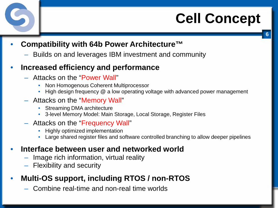
Cell Concept • Compatibility with 64b Power Architecture™
– Builds on and leverages IBM investment and community
• Increased efficiency and performance – Attacks on the “Power Wall”
• Non Homogenous Coherent Multiprocessor • High design frequency @ a low operating voltage with advanced power management
– Attacks on the “Memory Wall” • Streaming DMA architecture • 3-level Memory Model: Main Storage, Local Storage, Register Files
– Attacks on the “Frequency Wall” • Highly optimized implementation • Large shared register files and software controlled branching to allow deeper pipelines
• Interface between user and networked world – Image rich information, virtual reality – Flexibility and security
• Multi-OS support, including RTOS / non-RTOS – Combine real-time and non-real time worlds

7
Cell BE Processor Overview
• IBM, SCEI/Sony, Toshiba Alliance formed in 2000 • Design Center opened in March 2001 • Based in Austin, Texas • ~$400M Investment – 400 people • February 7, 2005: First technical disclosures • May 16, 2005: First public demonstrations at E3 • August 25, 2005: Release of technical documentation • Designed for Sony PlayStation3
– Commodity processor • Cell is an extension to IBM Power family of processors • Sets new performance standards for computation &
bandwidth • High affinity to HPC workloads
– Seismic processing, FFT, BLAS, etc.

8
The Cell BE Processor
© 2005 IBM Corporation 8

9
Cell BE Architecture™ Technology Competitive Roadmap
2006 2007 2008 2009 2010
Performance Enhancements/ Scaling
Enhanced Cell BE
(1+8eDP) 65nm SOI
Cell BE (1+8)
90nm SOI
Cost Reduction
1TF Processor 45nm SOI
Cell BE Roadmap Version 5.0 24-Jul-2006 All future dates are estimations only; Subject to change without notice.

10
Firmware
e.g. Blades, Development platforms, etc
Operating Systems such as Linux
e.g. SPE exploitation, BE awareness Device Drivers
Compilers
C, C++, Fortran, etc
Application Tooling and Environment Programming model/APIs for accelerators
Scale out Systems
Sector Specific Libraries
ISVs, Universities, Labs, Open Source, etc.
Applications
ISV, Universities, Labs, etc
HyperVisors
Core Libraries
e.g. SPE intrinsic, etc
Ubiquitous for all Markets
Market Segment Specific
SPE performance enhancements, improved scheduling and affinity management, SPE core files
libSPE cleanup and vector math support for SPEs security utilities
XLC GA with additional distro hosted platform coverage, Overlay support, gcc and xlC continued work on auto-vectorization/SIMDization,
xlC MASS/V support
Overlay support, Accelerated Library Framework (ALF) Performance tooling (oprofile, pmcount, VPA)
Gdbserver server support for combined PPE/SPE remote debugging IDE integration with programming models, compiler, debugger and
simulator support,
In addition: libraries, programming model and frameworks, performance tools, operating systemsf rom IBM Ecosystem, Mercury, Sony, PeakStream, RapidMind,
Yellow Dog
Cell based systems Software Stack

11
Cell BE™ Blade vs. SDK
Performance
2006 2008 2007
Cell BE-Based Blade
Advanced Cell BE-Based Blade
Enhanced Cell BE-based Blade
GA: 2H06
Target Availability: 2H07
Target Availability: 1H08
2 Cell BE Processors Single Precision Floating Pt Affinity 1 GB Memory Up to 4X PCI Express™
2 Cell BE Processors Single Precision Floating Pt Affinity 2 GB Memory Up to 16X PCI Express
2 Enhanced Cell BE Processors SP & DP Floating Point Affinity Up to 16 GB Memory Up to 16X PCI Express
Available: 17 July 2006
Target Availability: 1H07
Target Availability: 2H07
SDK 1.1 Alpha Software
Hardware
SDK 2.0
Beta Software
SDK 3.0
GA Software
Cell BE Roadmap Version 5.0 24-Jul-2006

12
Architecture

13
Cell Concept • Compatibility with 64b Power Architecture™
– Builds on and leverages IBM investment and community
• Increased efficiency and performance – Non Homogenous Coherent Chip Multiprocessor
• Allows an attack on the “Frequency Wall” – Streaming DMA architecture attacks “Memory Wall” – High design frequency, low operating voltage attacks
“Power Wall” – Highly optimized implementation
• Interface between user and networked world – Flexibility and security – Multi-OS support, including RTOS/non-RTOS – Architectural extensions for real-time management

14
Cell Architecture is …
COHERENT BUS
Power
ISA
MMU/BIU
Power
ISA
MMU/BIU
…
IO
transl. Memory
Incl. coherence/memory
compatible with 32/64b Power Arch. Applications and OS’s
64b Power Architecture™

15
Cell Architecture is … 64b Power Architecture™
COHERENT BUS (+RAG)
Power
ISA +RMT
MMU/BIU
+RMT
Power
ISA +RMT
MMU/BIU
+RMT
IO
transl. Memory
Plus
Memory
Flow Control (MFC)
MMU/DMA
+RMT
Local Store
Memory
MMU/DMA
+RMT
Local Store
Memory
LS Alias
LS Alias …
…
…
16
Cell Architecture is … 64b Power Architecture™+ MFC
COHERENT BUS (+RAG)
Power
ISA +RMT
MMU/BIU
+RMT
Power
ISA +RMT
MMU/BIU
+RMT
IO
transl. Memory
Plus
Synergistic
Processors
MMU/DMA
+RMT
Local Store
Memory
MMU/DMA
+RMT
Local Store
Memory
LS Alias
LS Alias …
…
… Syn.
Proc.
ISA
Syn.
Proc.
ISA

17
18
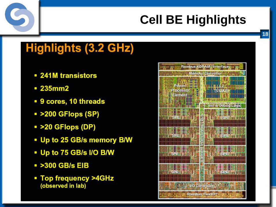
Cell BE Highlights

19
Cell BE vs Pentium D
• Combines multiple high performance processors in one chip
• 9 cores, 10 threads
• A 64-bit Power Architecture™ core (PPE)
• 8 Synergistic Processor Elements (SPEs) for data-intensive processing
• Current implementation—roughly 10 times the performance of Pentium for computational intensive tasks
• Clock: 3.2 GHz (measured at >4GHz in lab)
Cell Pentium D
Peak I/O BW 75 GB/s ~6.4 GB/s
Peak SP Performance
>200 GFLOPS ~30 GFLOPS
Area 235 mm² 206 mm²
Total Transistors 241M ~230M

20
Cell BE Processor Features
• Heterogeneous multi-core system architecture
– Power Processor Element for control tasks
– Synergistic Processor Elements for data-intensive processing
• Synergistic Processor Element (SPE) consists of
– Synergistic Processor Unit (SPU)
– Synergistic Memory Flow Control (SMF)
• Data movement and synchronization
• Interface to high-performance Element Interconnect Bus
16B/cycle (2x) 16B/cycle
BIC
FlexIOTM
MIC
Dual XDRTM
16B/cycle
EIB (up to 96B/cycle)
16B/cycle
64-bit Power Architecture with VMX
PPE
SPE
LS
SXU SPU
SMF
PXU L1
PPU
16B/cycle L2
32B/cycle
LS
SXU SPU
SMF
LS
SXU SPU
SMF
LS
SXU SPU
SMF
LS
SXU SPU
SMF
LS
SXU SPU
SMF
LS
SXU SPU
SMF
LS
SXU SPU
SMF
21
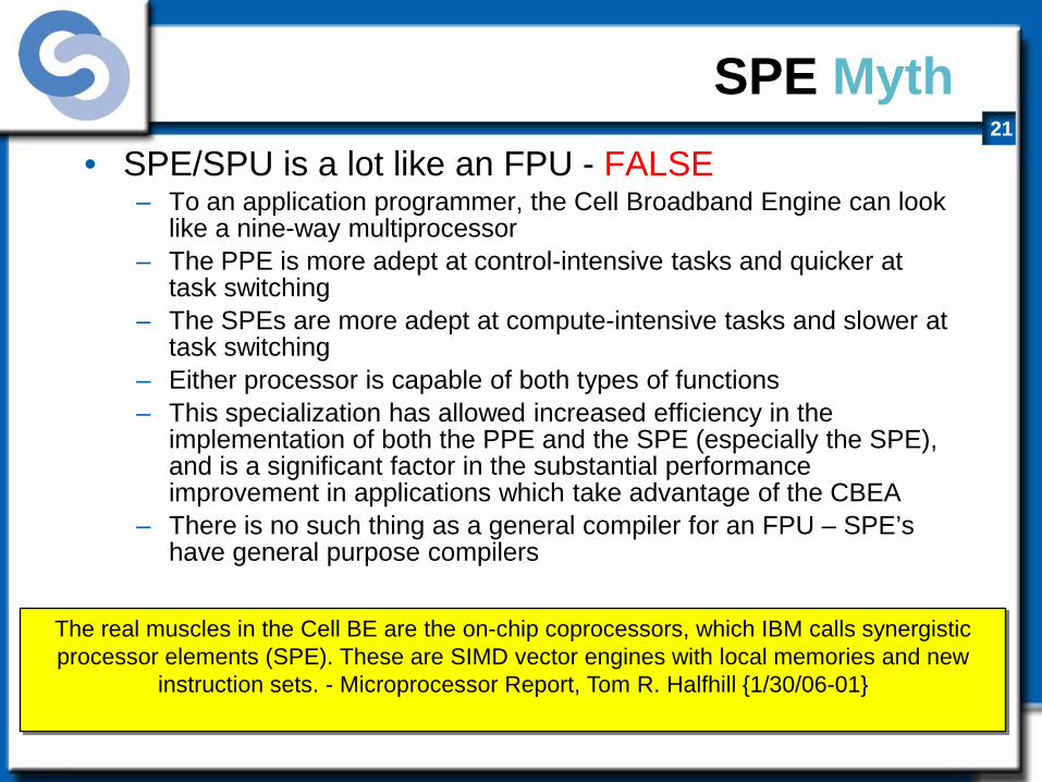
SPE Myth • SPE/SPU is a lot like an FPU - FALSE
– To an application programmer, the Cell Broadband Engine can look like a nine-way multiprocessor
– The PPE is more adept at control-intensive tasks and quicker at task switching
– The SPEs are more adept at compute-intensive tasks and slower at task switching
– Either processor is capable of both types of functions – This specialization has allowed increased efficiency in the
implementation of both the PPE and the SPE (especially the SPE), and is a significant factor in the substantial performance improvement in applications which take advantage of the CBEA
– There is no such thing as a general compiler for an FPU – SPE’s have general purpose compilers
The real muscles in the Cell BE are the on-chip coprocessors, which IBM calls synergistic processor elements (SPE). These are SIMD vector engines with local memories and new
instruction sets. - Microprocessor Report, Tom R. Halfhill {1/30/06-01}

22
Cell Double Precision Myth • The Cell Broadband Engine Chip doesn’t do Double
Precision (DP) – FALSE – The Cell BE chip does perform Double Precision compliant
with IEEE specifications, and does it rather fast – The Cell BE peak DP operations is 1.6x times faster than a
similarly clocked Intel Xeon – We tend not to talk about DP operations on Cell, because
they run at roughly 1/10th the speed of Single Precision operations, today
– There is a design for the Cell BE that retains the full SP performance, while bringing DP performance to 50% the speed of SP operations
– This design would produce a pin compatible chip, and is sometimes known as Cell DP
23
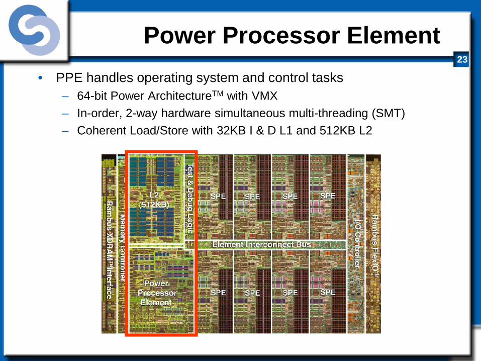
Power Processor Element • PPE handles operating system and control tasks
– 64-bit Power ArchitectureTM with VMX – In-order, 2-way hardware simultaneous multi-threading (SMT) – Coherent Load/Store with 32KB I & D L1 and 512KB L2

24
Pre-Decode
L1 Instruction Cache
Microcode SMT Dispatch (Queue)
Decode Dependency
Issue
Branch Scan
Fetch Control L2 Interface
VMX/FPU Issue (Queue)
VMX Load/Store/
Permute
VMX Arith./Logic Unit
FPU Load/Store
FPU Arith/Logic Unit
Load/Store Unit
Branch Execution
Unit
Fixed-Point Unit
FPU Completion VMX Completion
Completion/Flush
8
4
2 1
2 1 1 1 1
1 1 1
4 Thread A Thread B
Threads alternate fetch and dispatch cycles
Thread A
Thread B
Thread A
L1 Data Cache
2
PPE Block Diagram
25
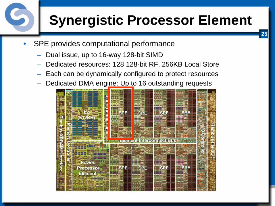
Synergistic Processor Element • SPE provides computational performance
– Dual issue, up to 16-way 128-bit SIMD – Dedicated resources: 128 128-bit RF, 256KB Local Store – Each can be dynamically configured to protect resources – Dedicated DMA engine: Up to 16 outstanding requests

26
Permute Unit Load-Store Unit
Floating-Point Unit Fixed-Point Unit
Branch Unit Channel Unit
Result Forwarding and Staging Register File
Local Store (256kB)
Single Port SRAM
128B Read 128B Write
DMA Unit
Instruction Issue Unit / Instruction Line Buffer
8 Byte/Cycle 16 Byte/Cycle 128 Byte/Cycle 64 Byte/Cycle
On-Chip Coherent Bus
SPE Block Diagram

27
SPE Highlights
• RISC like organization – 32 bit fixed instructions – Clean design – unified Register file
• User-mode architecture – No translation/protection within SPU – DMA is full Power Arch protect/x-late
• VMX-like SIMD dataflow – Broad set of operations (8 / 16 / 32
Byte) – Graphics SP-Float – IEEE DP-Float
• Unified register file – 128 entry x 128 bit
• 256KB Local Store – Combined Instruction & Data
LS
LS
LS
LSGPR
FXU ODD
FXU EVN
SFPDP
CO
NTR
OL
CHANNEL
DMA SMMATO
SBIRTB
BEB
FWD
14.5mm2 (90nm SOI)
28
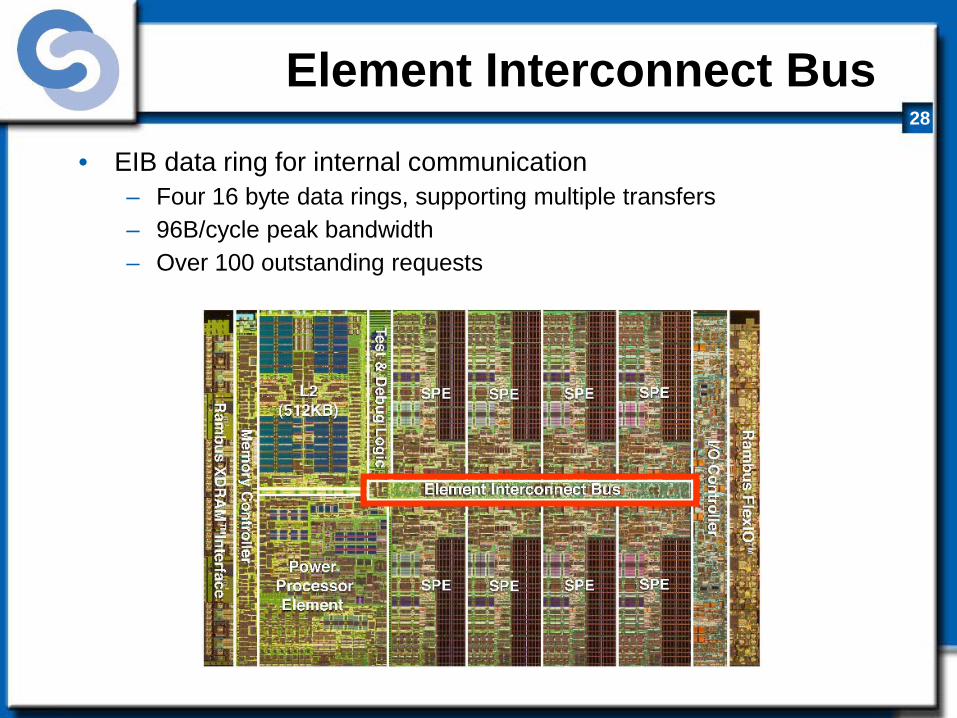
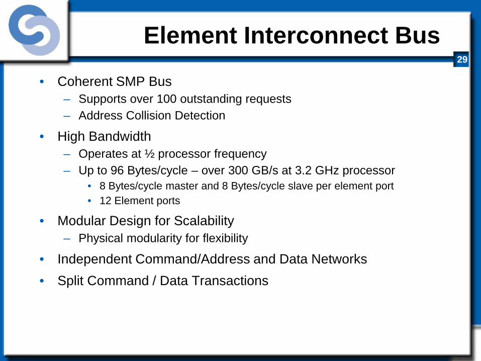
Element Interconnect Bus
• EIB data ring for internal communication – Four 16 byte data rings, supporting multiple transfers – 96B/cycle peak bandwidth – Over 100 outstanding requests
29
Element Interconnect Bus
• Coherent SMP Bus – Supports over 100 outstanding requests – Address Collision Detection
• High Bandwidth – Operates at ½ processor frequency – Up to 96 Bytes/cycle – over 300 GB/s at 3.2 GHz processor
• 8 Bytes/cycle master and 8 Bytes/cycle slave per element port • 12 Element ports
• Modular Design for Scalability – Physical modularity for flexibility
• Independent Command/Address and Data Networks • Split Command / Data Transactions

30
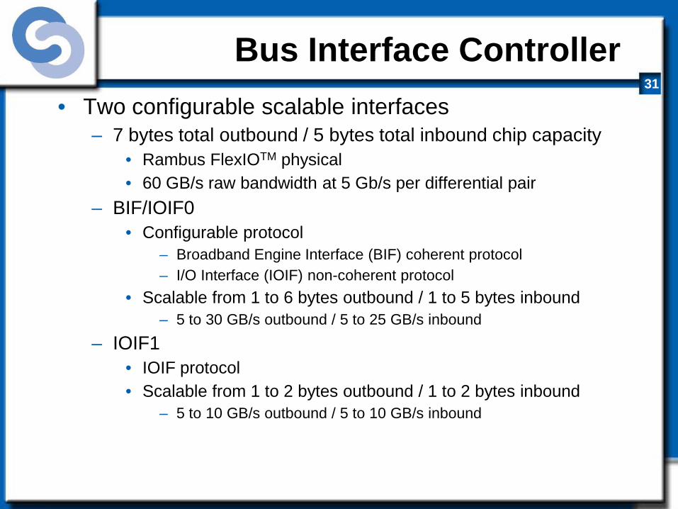
Bus Interface Controller
31
Bus Interface Controller • Two configurable scalable interfaces
– 7 bytes total outbound / 5 bytes total inbound chip capacity • Rambus FlexIOTM physical • 60 GB/s raw bandwidth at 5 Gb/s per differential pair
– BIF/IOIF0 • Configurable protocol
– Broadband Engine Interface (BIF) coherent protocol – I/O Interface (IOIF) non-coherent protocol
• Scalable from 1 to 6 bytes outbound / 1 to 5 bytes inbound – 5 to 30 GB/s outbound / 5 to 25 GB/s inbound
– IOIF1 • IOIF protocol • Scalable from 1 to 2 bytes outbound / 1 to 2 bytes inbound
– 5 to 10 GB/s outbound / 5 to 10 GB/s inbound

32
Bus Interface Controller • IOIF Mode Additional Features
– I/O Address Translation and Protection • Two stage segment table / page table lookup • 4KB, 64KB, 1MB, 16MB page size support per segment • Storage protection at page granularity • Storage protection by device ID • Command ordering attributes assigned at page granularity • HW and SW load of translation caches
– Four Virtual Channels • Independent ordering and resource management per VC
– Interrupt Controller • Interrupt presentation, routing and status to PPEs • Interprocessor Interrupt support • 16 priority levels

33
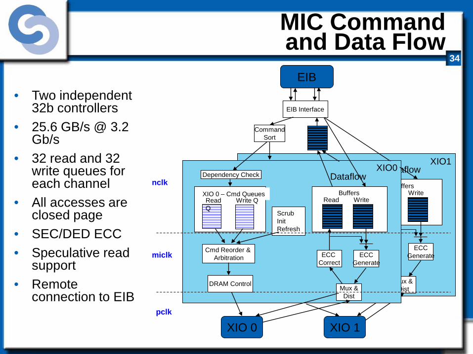
Dual XDRTM Controller (25.6 GB/s @ 3.2 Gbps)
34
MIC Command and Data Flow
Read Write Buffers XIO 0 – Cmd Queues
Read Q
Write Q
Scrub Init Refresh
Cmd Reorder & Arbitration
DRAM Control
ECC Correct
ECC Generate
Mux & Dist
Dependency Check Dataflow
Read Write Buffers XIO 0 – Cmd Queues
Read Q
Write Q
Scrub Init Refresh
Cmd Reorder & Arbitration
DRAM Control
ECC Correct
ECC Generate
Mux & Dist
Dependency Check Dataflow
EIB
EIB Interface
Command Sort
XIO 0 XIO 1
nclk
miclk
pclk
XIO1 XIO0
• Two independent 32b controllers
• 25.6 GB/s @ 3.2 Gb/s
• 32 read and 32 write queues for each channel
• All accesses are closed page
• SEC/DED ECC • Speculative read
support • Remote
connection to EIB

35
Cell Processor
Power Processor Element (PPE): •General Purpose, 64-bit RISC Processor (PowerPC 2.02) •2-Way Hardware Multithreaded •L1 : 32KB I ; 32KB D •L2 : 512KB •Coherent load/store •VMX •3.2 GHz
Internal Interconnect: •Coherent ring structure •300+ GB/s total internal interconnect bandwidth •DMA control to/from SPEs supports >100 outstanding memory requests
Synergistic Processor Elements (SPE): •8 per chip •128-bit wide SIMD Units •Integer and Floating Point capable •256KB Local Store •Up to 25.6 GF/s per SPE --- 200GF/s total *
External Interconnects: •25.6 GB/sec BW memory interface •2 Configurable I/O Interfaces
•Coherent interface (SMP) •Normal I/O interface (I/O & Graphics) •Total BW configurable between interfaces •Up to 35 GB/s out •Up to 25 GB/s in
Memory Management & Mapping •SPE Local Store aliased into PPE system memory •MFC/MMU controls SPE DMA accesses
•Compatible with PowerPC Virtual Memory architecture •S/W controllable from PPE MMIO
•Hardware or Software TLB management •SPE DMA access protected by MFC/MMU
“Supercomputer-on-a-Chip”
* At clock speed of 3.2GHz
Element Interconnect Bus
MFC
Local Store
SPU
N
AUC
MFC
Local Store
SPU
N
AUC
Power Core (PPE)
L2 Cache
NCU Local Store
SPU MFC
N
AUC
Local Store
SPU MFC
N
AUC
N N
N N
MFC
Local Store
SP
U
N
AU
C
MFC
Local Store
SP
U
N
AU
C
MFC
Loca
l Sto
re
SP
U
N
AU
C
MFC
Loca
l Sto
re
SP
U
N
AU
C
20 GB/sec Coherent
Interconnect
25.6 GB/sec Memory Inteface
5 GB/sec I/O Bus

36
Cell BE Processor Can Support Many Systems
• Game console systems • Blades • HDTV • Home media servers • Supercomputers • And more!
Cell BE Processor
XDRtm XDRtm
IOIF0 IOIF1
Cell BE Processor
XDRtm XDRtm
IOIF BIF
Cell BE Processor
XDRtm XDRtm
IOIF
Cell BE Processor
XDRtm XDRtm
IOIF BIF
Cell BE Processor
XDRtm XDRtm
IOIF
Cell BE Processor
XDRtm XDRtm
IOIF
BIF
Cell BE Processor
XDRtm XDRtm
IOIF SW

37
The First Generation Cell Blade
Cell Processors 1GB XDR Memory IO Controllers IBM Blade Center interface

38
Cell Blade Hardware Overview
Chassis
Blade • Blade
• Two Cell BE Processors • 1GB XDRAM • BladeCenter Interface ( Based on IBM JS20)
• Chassis
• Standard IBM BladeCenter form factor with: • 7 Blades (for 2 slots each) with full performance • 2 switches (1Gb Ethernet) with 4 external ports
each • Updated Management Module Firmware. • External Infiniband Switches with optional FC ports. •
• Typical Configuration (available today from E&TS) • eServer 25U Rack • 7U Chassis with Cell BE Blades, OpenPower 710 • Nortel GbE switch • GCC C/C++ (Barcelona) or XLC Compiler for Cell (alphaworks) • SDK Kit on http://www-128.ibm.com/developerworks/power/cell/
Blade
BladeCenter Network Interface
Cell Processor
South Bridge
XDRAM
Cell Processor
South Bridge
XDRAM
IB 4X
IB 4X
GbE GbE