a.saez j.ortiz ade - esg g.siringo r. price j.castillo
TRANSCRIPT

ALMA System Block Diagram
SYSE-80.04.01.00-004-R-DWG
Version: R
Status: Draft
01 April 2021
Prepared by: Organization: Date:
J.Ortiz
A.Saez
G.Siringo
R. Price
J.Castillo (2016)
ADE - ESG
01 April 2021
Approved by:
Tzu-Chiang Shen (JAO ESG Manager)
Released by:
Norikazu Mizuno (ADE Head)

H
G
F
E
D
C
B
A
8 7 6 5 4 3 2 1
H
G
F
E
D
C
B
A
8 7 6 5 4 3 2 1
Atacama Large Millimeter Array (ALMA)
System Block Diagram
Change RecordSIZE DWG NO REV
B 80.04.01.00-004 R
SCALE 1 : 1 01 April 2021 SHEET 1 OF 8The ALMA System Block Diagram is a joint effort
by the ALMA Project Team.
CONTACT:
Norikazu Mizuno
Change # Sheet Location Update on diagram
1 Cover Signature Matrix update
2 Change Record Listed changes on Rev R. Contact person updated. Date updated.
3 Central Electronics Contact persons and sheet date updated
4 Central Electronics A5-B5 CAN configuration for the Laser synthesizer 4-6 was updated
5 Central Electronics C4 Backup Master Laser connection was updated
6 Central Electronics B3-B4 Hydrogen MASER was included with its connections
7 Central Electronics C2 AMB configuration updated
8 Central Electronics 4C Master Laser Distributor (MLD) Optical Divider updated from “1:6” to “1:6(8)”
9 Central Electronics 5A-5B-5C-5D Photonic Reference Distributor (PRD) Optical Power Divider Updated from “1:80” to “1:66 (80)”
10 Central Electronics B3 5MHz and 10MHz labels added to H-Maser and Rb-MFS outputs
11 Central Electronics B4 Product ID added to 10MHz distributor
12 Central Electronics A4-B4 125MHz distributor product ID update
13 Central Electronics F8 Switch from EDFAs and spectrum analyzer diagrams removed since not yet installed.
14 CLOA Racks Contact person and sheet date updated
15 CLOA Racks D6-D7 Hydrogen MASER Rack was added
16 Antenna Electronics Contact persons and sheet date updated
17 Antenna Electronics H7 Band 1 sky frequency range changed from “31.3-45GHz” to “35-50GHz (52)”
18 Antenna Electronics G7 Band 1 LO driver & YTO range changed from “27.3-33.0 GHz” to “31-40GHz”
19 Antenna Electronics H7-G7 Band 1 Mixers were moved from CCA1 to WCA1. Amplifiers added at WCA1 after Mixers for both POLs
20 Antenna Electronics H5 Band 5 sky frequency range changed from “163.0-211.0” GHz to “158-211GHz”
21 Antenna Electronics G5 Band 5 Extended the 110K stage to include the “x2” multipliers
22 Antenna Electronics G5 Band 5 Deleted amplifiers and “x3” multipliers
23 Antenna Electronics G5 Band 5 LO driver range changed from “28.5-34GHz” to “83.0-101.5GHz”
24 Antenna Electronics G5 Band 5 Warm multiplier changed from “x2” to “x6”
25 Antenna Electronics G5 Band 5 YTO range changed from “14-17GHz” to “13.8-16.9GHz”
27 Baseline Correlator Contact person and sheet date updated
28 Baseline Correlator D2-E2 Phase Interface Cards
29 Baseline Correlator D1 OFL multiplexer added
30 VLBI Recorders Recorders
31 VLBI Recorders OFL Demultiplexer
32 ACA Correlator Contact person and sheet date updated
33 ACA Correlator F3-F5 Number of DFP(8) and CIP(4) modules per quadrant added
35 ACA Correlator E5-E6 Digital Power Meter included
36 ACA Correlator E3-F3 DIP Enclosures explicitly added to the diagram
37 ACA Correlator E3-E4-E5-E6 Correlator Monitor and Control Bus (CMB) bus is constrained as a private quadrant network
38 ACA Correlator D6-E6-F6 "Baseband" label replace with "BBpr" for diagram consistency
39 Patch Panel Contact person and sheet date updated
40 Cryostat Contact person and sheet date updated
Quadrants names and numbering changed from
“Set #1”, “Set #2”, “Set #3 and “Set #4”
To
“Quadrant 0”, “Quadrant 1”, “Quadrant 2” and “Quadrant 3”
D3-E3-F3 ACA Correlator 34
Band 6 IF output lines changed from
{
B6-P0: 5 - 10 GHz
B6-P0: 5 - 10 GHz
B6-P1: 5 - 10 GHz
B6-P1: 5 - 10 GHz
}
To
{
B6-P0: 4.5 - 10 GHz
B6-P0: 4.5 - 10 GHz
B6-P1: 4.5 - 10 GHz
B6-P1: 4.5 - 10 GHz
}
4FAntenna Electronics 26
New on Rev. R

Foundation
Vault
Fiber Splice
Box (SB)
(8:8 Fiber)
First LO Offset
Generator
FLOOG55.07
2x2 M
atrix
S
witc
h
2x2 M
atrix
S
witc
h2x2 M
atrix
S
witc
h
2.1-3.9 GHz
Anti-alias
Front End
4-K
Sta
ge
x 3 x 3
x 6
YIG
OscPLL
Cold optics
4-K
Sta
ge
x 6 x 6
x 3
YIG
OscPLL
Cold optics
&
Polarization Separating Grids
4-K
Sta
ge
x 9 x 9
x 3
YIG
OscPLL
Cold optics
4-K
Sta
ge
B10
-P0
: 4 -
12
GH
z
B10
-P1
: 4 -
12
GH
z
x 6
YIG
OscPLL
LO Injection
Optics
LO Injection
Optics
Cold optics
Ortho Mode
Transducer
4-K
Sta
ge
x 3 x 3
B6
-P0
: 4
.5 -
10
GH
z
B6
-P1
: 4
.5 -
10
GH
z
x 6
YIG
OscPLL
Cold optics
Ortho Mode
Transducer
4-K
Sta
ge
x 2 x 2
x 6
YIG
OscPLL
Cold optics
Ortho Mode
Transducer
4-K
Sta
ge
x 2 x 2
x 3
YIG
OscPLL
Cold optics
Ortho Mode
Transducer
4-K
Sta
ge
x 6
YIG
OscPLL
Cold optics
Ortho Mode
Transducer
YIG
OscPLL
B9
-P0
: 4 -
12
GH
z
B9
-P1
: 4 -
12
GH
z
B8
-P0
: 4 -
8 G
Hz
B8
-P1
: 4 -
8 G
Hz
B5
-P0
: 4 -
8 G
Hz
B5
-P1
: 4 -
8 G
Hz
B4
-P0
: 4 -
8 G
Hz
B4
-P1
: 4 -
8 G
Hz
2SB
SIS mixer
2SB
SIS mixer
B3
-P0
: 4 -
8 G
Hz
B3
-P1
: 4 -
8 G
Hz
B3
-P0
: 4 -
8 G
Hz
B3
-P1
: 4 -
8 G
Hz
HFETHFET
B1
-P0
: 4 -
12
GH
z
B1
-P1
: 4 -
12
GH
z
IF Switch Module IF Switch Module
Protocol Encoder
16:1 MUXHalf
Transponder23C
16:1 MUXHalf
Transponder 25D
Digitizer 53.01
35.0–50.0(52.0) GHz
IF P
rocesso
r P
0
IF
P
52.0
1
LNA
Gain
Equalizer
Total Pwr USB Detector
LNA
Gain
Equalizer
Total Pwr LSB Detector
Gain 0: 0-31.5 dB
0.5 dB step
Gain
Equalizer
2.1-3.9 GHz
Anti-alias
0.5 dB stepGain
Equalizer
2.1-3.9 GHz
Anti-alias
0.5 dB stepGain
Equalizer
2.1-3.9 GHz
Anti-alias
0.5 dB stepGain
Equalizer
5:1 MUX
3 b
it
A/D
3 b
it
A/D
8.5 GHz LPF
12 GHz LPF
8.5 GHz LPF
12 GHz LPF
4-12 GHz
BPF
4-12 GHz
BPF
1:4 Demux
1:1
6D
em
ux
1:1
6D
em
ux
1:1
6D
em
ux
1:1
6D
em
ux
1:1
6D
em
ux
1:1
6D
em
ux
Atacama Large Millimeter Array (ALMA)
System Block Diagram
Antenna ElectronicsSIZE DWG NO REV
E 80.04.01.00-004 R
SCALE 1 : 1 01 April 2021 SHEET 3 OF 8The ALMA System Block Diagram is a joint effort
by the ALMA Project Team.
CONTACT:
LO2 BB0
x 9x 9
31.0 – 40.0 GHz
Cold optics
Ortho Mode
Transducer
YIG
OscPLL
HFETHFET
B2
-P0
: 4 -
12
GH
z
B2
-P1
: 4 -
12
GH
z
Band 2
67.0 - 90.0 GHz
13.2-15.7 GHz
Band 3
84.0 - 116.0 GHz
15.3-18.0 GHz
Band 4
125.0 - 163.0 GHz
22.2-25.8 GHz
Band 5
158.0 - 211.0 GHz
13.8-16.9 GHz
Band 6
211.0 - 275.0 GHz
12.3-14.7 GHz 15.62-20.37 GHz
Band 7
275.0 - 373.0 GHz
21.72-27.44 GHz
Band 8
385.0 - 500.0 GHz
Band 9
602.0 - 720.0 GHz
22.51-26.45 GHz
DSB
SIS mixer
DSB
SIS mixer
DSB
SIS mixer
DSB
SIS mixer
14.8 -17.4 GHz
Band 10
787.0 - 950.0 GHz
Va
cuu
m V
esse
l B
ou
nd
ary
Wa
ll
Va
cuu
m V
esse
l B
ou
nd
ary
Wa
ll
2SB
SIS mixer
2SB
SIS mixer
B7
-P0
: 4 -
8 G
Hz
B7
-P1
: 4 -
8 G
Hz
B7
-P0
: 4 -
8 G
Hz
B7
-P1
: 4 -
8 G
Hz
LO2
Synthesizer
Slot BBpr2
x 6
Mechanism for inserting Calibration, Solar Protection and Polarization Device 40.06
Window
2SB
SIS mixer
2SB
SIS mixer
900 Hybrid
2SB
SIS mixer
2SB
SIS mixer2SB
SIS mixer
2SB
SIS mixer
900 Hybrid 90
0 Hybrid
Polarization 0
USB
Polarization 0
LSB
Polarization 1
USB
Polarization 1
LSB
Front End Monitor & Control
(FE M/C) 40.04.03
1 bit @ 4 Gb/s
1bit@ 10Gbps (2 Pol)
AMB2
G.Siringo, A.Saez, J.Ortiz
H
G
F
E
D
C
B
A
8 7 6 5 4 3 2 1
H
G
F
E
D
C
B
A
8 7 6 5 4 3 2 1
Cold optics
Polarization Separating Grid
110 K and 15 K IR Filters
Window
110 K and 15 K IR Filters
Window
110 K and 15 K IR Filters
Window
Polarization Separating Grid
110 K and 15 K IR Filters
Window
110 K and 15 K IR Filters
Window
110 K and 15 K IR Filters
Window
110 K and 15 K IR Filters
Window
110 K and 15 K IR Filters
Window
110 K and 15 K IR Filters
Window
110 K and 15 K IR Filters
900 Hybrid 90
0 Hybrid
LSB IF Input
4 - 12 GHz
2 - 4 GHz
2 - 4 GHz
B4
-P1
: 4 -
8 G
Hz
B4
-P0
: 4 -
8 G
Hz
B5
-P1
: 4 -
8 G
Hz
B5
-P0
: 4 -
8 G
Hz
B6
-P0
: 4
.5 -
10
GH
z
B6
-P1
: 4
.5 -
10
GH
z
Warm Optics Warm Optics Warm Optics
Optical Pointing Telescope(not on all antennas)
BE Digital Rack
AMB2
AM
B1
AM
B1
AM
B1
31.0 – 40.0 GHzLO Driver 1
79.0 - 94.0 GHzLO Driver 2
92.0 - 108.0 GHzLO Driver 3
66.5 - 77.5 GHzLO Driver 4
83.0-101.5 GHzLO Driver 5
73.7 - 88.3 GHzLO Driver 6
94.3 - 121.7 GHzLO Driver 7
65.5 - 82.0 GHzLO Driver 8
67.8 - 79.1 GHzLO Driver 9
88.3 - 104.7 GHzLO Driver 10
M/C Signals
Ethernet Signals
Video Signals
Other Signals
Timing References
Legend
RF Signals
LO Signals
DTS Signals
12
5 M
Hz
12
5 M
Hz
12
5 M
Hz
48
msec
48
msec
48
msec
Fine Tune
Synthesizer
20-45 MHz
125 MHz
P1 LSB
P1 USB
Formatter 53.05
DTS Transmitter DTX - BBpr0 53.08.02
DTS Transmitter DTX - BBpr1 53.08.03
AMP
AMP
AMP
AMP
Low
Pass
Filters
Total
Power
Digitizers
Transmitter&
ReceiverBuffers
Total Power Digitizer, Monitor & Control Board
TPD&MC 52.07
SPI
SPI
Rabbit
Core
Module
(RCM)
Buffers
AMBSI-2
IF Switch ControlerIF Switch Module
DC
Pow
er
Su
pp
ly
40.0
4.0
1
Warm Optics
Bias Filter Card
Cartridge Bias Module
40.04.02
Bias Filter Card
Cartridge Bias Module
40.04.02
Bias Filter Card
Cartridge Bias Module
40.04.02
Bias Filter Card
Cartridge Bias Module
40.04.02
Bias Filter Card
Cartridge Bias Module
40.04.02
Bias Filter Card
Cartridge Bias Module
40.04.02
Bias Filter Card
Cartridge Bias Module
40.04.02
Bias Filter Card
Cartridge Bias Module
40.04.02
Bias Filter Card
Cartridge Bias Module
40.04.02
15
-K S
tag
e
11
0-K
Sta
ge
Bias Filter Card
Cartridge Bias Module
40.04.02
Cold
Cart
ridg
e A
ssem
bly
40.0
2.0
9
Cold
Cart
ridg
e A
ssem
bly
40.0
2.1
0
Cold
Cart
ridg
e A
ssem
bly
40.0
2.0
8
Cold
Cart
ridg
e A
ssem
bly
40.0
2.0
7
Cold
Cart
ridg
e A
ssem
bly
40.0
2.0
6
Cold
Cart
ridg
e A
ssem
bly
40.0
2.0
5
Cold
Cart
ridg
e A
ssem
bly
40.0
2.0
4
Cold
Cart
ridg
e A
ssem
bly
40.0
2.0
3
Cold
Cart
ridg
e A
ssem
bly
40.0
2.0
2
Warm
Cart
ridg
e A
ssem
bly
40.1
0.0
1C
old
Cart
ridg
e A
ssem
bly
40.0
2.0
1
Line
Filter
48V DC > Digital BE Rack DTS Load
PSA
AC-penta-DC
Power Supply Over-Temp Cutout
-7 V
+7 V
-17 V
+17 Vb
+17 Va
Surge
Protector
AC - 48V DC
Power Supply PSD
Over-Temp Cutout
16:1 MUXHalf
Transponder 21B
Protocol Encoder
5:1 MUX1:4 Demux
Protocol Encoder
5:1 MUX1:4 Demux
16 bits@ 625 Mbps
80 bits@ 62.5 Mbps (2 Pol)
64 bits@ 62.5 Mbps
16 bits@ 250 Mbps
250 MHzStep Phase
LVDS
to RS
422
48
ms
LV
DS
Differential DDS
Accumulator
48
ms
Con
trol
LUT
LUT
LPF
LPF
90° 0° 90° 0°
I/Qmod
I/Qmod
x2
Phase Comp.
4GHzVCO
Lo
ck
Vo
ltag
e
PS
_V
oltag
e
RF Subassembly
4 GHzStep Phase
12
5 M
Hz
0 d
Bm
Digitizer Clock Assembly DGCK 53.04
8
AD
AD
2
250 MHz4 GHz
48 msec
AM
B1
DTS Transmitter DTX - BBpr2 53.08.04
DTS Transmitter DTX - BBpr3 53.08.05
Formatter 53.05Digitizer 53.01
250 MHz4 GHz
Digitizer 53.01
48 msec
Formatter 53.05
250 MHz4 GHz
Digitizer 53.01
48 msec
Formatter 53.05
48 msec
125
MH
z
AMB1
BB0
BB1
BB2
BA_Det
BB_Det
BC_Det
BD_Det
BB0
8 - 14 GHz+14 to +18 dBm
FTS
DYTO
8-14 GHz
Course Tuning Control
Fine Tune Driver
DAC
-3dB
+19dB
14.2 GHz
A
PowerDetect
PowerDetect
PowerDetect
Lock Detect
Monitor
DCVoltages
M&CInterface
Control
A
50 MHz
-5dB
50 MHz
Det
fLoop Filter
AMB1LO Reference Receiver LORR 55.04
125 MHz BPF
Comb
Gen
125 MHz
40 Hz BW
H(s)
FPGA:
48 msec Det.
Lock Detect.
RF Detectors
M&C
48m
s (R
S4
22)
48ms (LVDS)
2.125 GHz
Amp
Equalizer
To ABM
LR
I
48 msec
AMB1
Ethernet Switch(located on azimuth platform;
managed)
Utility Module(located on azimuth platform)
Nutator Controller(not on all antennas; located on azimuth platform)
Antenna Control Unit (ACU) (located on azimuth platform)
Mu
lti-f
iber
cable
to A
OS
Tech
nic
al B
uild
ing
Azimuth WrapsElevation Wraps
Nutator (located at quadrapod apex; not on all antennas)
He Compressor
(for detailed I/F’s see Cryostat Blockdiagram)
AMB5
Antenna Bus Master (ABM)(located in digital rack)
Sp
are
/Deb
ug
gin
g
Op
tica
l T
ele
sco
pe
Az. P
latf
orm
AP
EX
/ H
olo
gra
ph
y
Rece
ive
r C
ab
in (
BE
Eq
)
Antenna
PAD
Fiber
Connector
Box (SB1)
(8:8 Fiber)
Ethernet Switch
(unmanaged)
Remote
Power
Switch
Antenna Cabin
Fiber Splice Box
(SB4)
(7:3 Fiber)
3dB Optical Coupler
1x10 Optical Switch
Fiber Freq. Shifter
Faraday Rotator Mirror
MC
PA
OA
AM
B1
AM
B3
AM
B18
AM
B5
FLOOG
Distributor
20-45 MHz 40.04.10
DC Pwr
125MHz
EFC
P0 LSB
P0 USB
ExternalMemory
FIFO
Time Stamp
Timing, Monitor & Control
EthernetControllerInterfaceA
ccum
ula
tors
Dig
itize
rIn
terface
Data
Rem
ap
Accu
mu
lato
rs
FPGA
2SB
SIS mixer
2SB
SIS mixer
B8
-P0
: 4 -
8 G
Hz
B8
-P1
: 4 -
8 G
Hz
AM
B1
BE Analog Rack
AMB2
AM
B2
AMB3
Fire Alarm
Emergency-Stop
AC Power Off
UPS Power Off
Stow Monitor
Over-Temp. Alarm
Discrete I/O Control
Fib
er
Op
tic M
ultip
lexe
r
DW
DM
FO
M
LO Photonic
Receiver
56.05
BB7BB5
BB3BB1
Total Power Digitizer, Monitor & Control Board
TPD&MC 52.00.04
AMB1
HT 27B
HT 29C
HT 31D
HT 33B
HT 35C
HT 37D
HT 39B
HT 41C
HT 43D
AM
B1
AM
B1
AM
B1
Line
Filter
Surge
ProtectorAC Input
230V 50 Hz
AMB1
AC Input
230V 50 Hz
Rece
ive
r C
ab
in (
FE
Eq)
AM
B2
AM
B4
48m
s (R
S4
22)
Fro
m L
O R
efe
rence
Rece
iver
LO Fiber
HVAC Alarm
Zenith Pointing
Feed Shutter
Spare
Spare
Spare
Wate
r V
apo
r R
adio
me
ter
40
.07
.00
Indoor
Control Unit
Compressor
M & C
AMB3
10:1 Switch
IF Switch Module
Eq.
Cryostat Monitor & Control
Vacuum pumps (on/off)Vacuum valvesVacuum vessel pressure
FE M/C
125 MHz
11
0-K
Sta
ge
11
0-K
Sta
ge
11
0-K
Sta
ge
11
0-K
Sta
ge
11
0-K
Sta
ge
11
0-K
Sta
ge
11
0-K
Sta
ge
11
0-K
Sta
ge
11
0-K
Sta
ge
15
-K S
tag
e
15
-K S
tag
e
15
-K S
tag
e
15
-K S
tag
e
15
-K S
tag
e
15
-K S
tag
e
15
-K S
tag
e
15
-K S
tag
e
15
-K S
tag
e
DC Pwr
DC Pwr
Warm
Cart
ridg
e A
ssem
bly
40.1
0.0
3
Warm
Cart
ridg
e A
ssem
bly
40.1
0.0
4
Warm
Cart
ridg
e A
ssem
bly
40.1
0.0
5
Warm
Cart
ridg
e A
ssem
bly
40.1
0.0
6
Warm
Cart
ridg
e A
ssem
bly
40.1
0.0
7
Warm
Cart
ridg
e A
ssem
bly
40.1
0.0
8
Warm
Cart
ridg
e A
ssem
bly
40.1
0.0
9
Warm
Cart
ridg
e A
ssem
bly
40.1
0.1
0
FE M/C
DC Pwr
FE M/C
DC Pwr
FE M/C
DC Pwr
FE M/C
DC Pwr
FE M/C
DC Pwr
FE M/C
DC Pwr
FE M/C
DC Pwr
FE M/C
DC Pwr
FE M/C
DC Pwr
FE M/C
DC Pwr
DC DC DC DC DC DC DC DC DCDC
AC Input
230V 50 Hz
Holography Receiver
USB IF Input
4 - 12 GHzS
S
AMP
AMP
S
S
AMP
analog dif ferential AMP
AMP
AMP
AMP
AMPAMP
AMP AMP
AMP
AMP
AMP
AMP
AMP
AMP
AMP
AMP
S
S
S
S
AMP
AMP
AMP
AMP
AMP
Gain 1: 0-31.5 dB
Gain 2: 0-31.5 dB
Gain 3: 0-31.5 dB
R
R
R
RL
L
L
LI
I
I
I
BB2
BB4
BB6
AMP
analog dif ferential
S
AC Input
230V 50 Hz
differential
differential
differential
differential
AM
P
AM
P
AM
P
AM
P
1.5 - 5 GHz
BPF
1.5 - 5 GHz
BPF
1.5 - 5 GHz
BPF
1.5 - 5 GHz
BPF
S
LO2 55.05
Synthesizer
Slot BBpr3
Holography
Support
Electronics25 MHz
48V DC
: Spare Fiber.
: Spare Fiber not installed.
Note: If not indicated as MMF,
all Fibers are SMF.
MMF
Telephones,Laptops, etc.
DC Pwr
DC Pwr
Front End
FE M/C
FE M/C
LO2
Synthesizer
Slot BBpr1
LO2
Synthesizer
Slot BBpr0
LO2 BB2LO2 BB4
LO2 BB6
LO2 BB1LO2 BB3
LO2 BB5LO2 BB7
8 - 14 GHz+14 to +18 dBm
I/O Board, Voltage-Conversion, M&C IF Downconverter P0
IFDC 52.06
IF Downconverter P1
IFDC 52.06
IF P
rocesso
r P
1
IF
P
52.0
0
AMB1
Private CAN
48 msec
AMB3
temporary connections
AMP
125
MH
z125
MH
z125
MH
z
/ 4250 MHz
62.5
MHz
54.0
2
1532 nm
~ 1557 nm
On Axis FOW On Axis FOW 54.09.02
57.03.01
57.03.03
FE M/CDC Power
M&C Module
40.04.07
DC Power
Distribution Module
40.04.08
Optical Diplexer
ODF 56.10
8 GHz SSB,
USB centred at 8 GHz
8 GHz SSB,
LSB centred at 8 GHz
Splice
Box
(SB3)
Splice
Box
(SB2)
“keep-alive”
“keep-alive”Diplexer
LORRD 55.10
25 MHz to LOPR
H(s)
Amp 1.5 GHz HPF
2 GHz
RF detect.
RF detect.
EFC
4 x HPF 4.16 GHz inside
analog rack penetration panel
Ortho Mode
Transducer
900 Hybrid
900 Hybrid 90
0 Hybrid
AMP
AMP
AMP
900 Hybrid 90
0 Hybrid 90
0 Hybrid 90
0 Hybrid
-31 to -18 dBm
-1 to +1 dBm input
-1 to +
1 d
Bm
input
AM
B1
Warm
Cart
ridg
e A
ssem
bly
40.1
0.0
2
40.04.06IF switch40.08.01
Band 1

Master
Laser1556.21 nm
ACA Patch
Panel
Main Patch
Panel Rack 3
Ant 2, BB1, Polarization 1
Data samples packet ized into
32 bit words @125k samples/1msec
Ant 2, BB1, Polarization 1
Data samples packet ized into
32 bit words @125k samples/1msec
Ant 2, BB0, Polarization 0
Data samples packet ized into
32 bit words @125k samples/1msec
Ant 2, BB0, Polarization 0
Data samples packet ized into
32 bit words @125k samples/1msec
Ant 1, BB1, Polarization 1
Data samples packet ized into
32 bit words @125k samples/1msec
Ant 1, BB1, Polarization 1
Data samples packet ized into
32 bit words @125k samples/1msec
Ant 1, BB0, Polarization 0
Data samples packet ized into
32 bit words @125k samples/1msecPacketizing &
Tracking
Delay
Station Card
1:16 Demux
1:16 Demux
1:16 Demux
16 bits @ 625 MHz
16 bits @ 625 MHz
16 bits @ 625 MHz
Packetizing &
Tracking
Delay
Station Card
16 bits @ 625 MHz
16 bits @ 625 MHz
16 bits @ 625 MHz
Ant 1, BB0, Polarization 0
Bit 1 of 2 bit sample
32 parallel signals @ 125 MHz
Ant 1, BB0, Polarization 0
Bit 2 of 2 bit sample
32 parallel signals @ 125 MHz
Ant 1, BB1, Polarization 1
Bit 1 of 2 bit sample
32 parallel signals @ 125 MHz
Ant 1, BB1, Polarization 1
Bit 2 of 2 bit sample
32 parallel signals @ 125 MHz
Ant 2, BB0, Polarization 0
Bit 1 of 2 bit sample
32 parallel signals @ 125 MHz
Ant 2, BB0, Polarization 0
Bit 2 of 2 bit sample
32 parallel signals @ 125 MHz
Ant 2, BB1, Polarization 1
Bit 1 of 2 bit sample
32 parallel signals @ 125 MHz
Ant 2, BB1, Polarization 1
Bit 2 of 2 bit sample
32 parallel signals @ 125 MHz
1:16 Demux
1:16 Demux
1:16 Demux
Corr
. C
ard
Corr
. C
ard
Corr
. C
ard
Corr
. C
ard
LTA
Card
Antenna 1, BBpr0, Polarization 0 & 1
Antenna 2, BBpr0, Polarization 0 & 1
Antenna 1, BBpr1, Polarization 0
Antenna 2, BBpr1, Polarization 1
Ant 1, BB0, Polarization 1
Packetized samples
@ 125,000 samples/1 msec
Corr
. C
ard
Corr
. C
ard
Corr
. C
ard
Corr
. C
ard
Corr
. C
ard
Corr
. C
ard
Corr
. C
ard
Corr
. C
ard
LTA
Card
Corr
. C
ard
Corr
. C
ard
Corr
. C
ard
Corr
. C
ard
Corr
. C
ard
Corr
. C
ard
Corr
. C
ard
Corr
. C
ard
LTA
Card
Corr
. C
ard
Corr
. C
ard
Corr
. C
ard
Corr
. C
ard
Corr
. C
ard
Corr
. C
ard
Corr
. C
ard
Corr
. C
ard
LTA
Card
Corr
. C
ard
Corr
. C
ard
Corr
. C
ard
Corr
. C
ard
Corr
. C
ard
Corr
. C
ard
Corr
. C
ard
Corr
. C
ard
LTA
Card
Corr
. C
ard
Corr
. C
ard
Corr
. C
ard
Corr
. C
ard
Corr
. C
ard
Corr
. C
ard
Corr
. C
ard
Corr
. C
ard
LTA
Card
Corr
. C
ard
Corr
. C
ard
Corr
. C
ard
Corr
. C
ard
Corr
. C
ard
Corr
. C
ard
Corr
. C
ard
Corr
. C
ard
LTA
Card
Corr
. C
ard
Corr
. C
ard
Corr
. C
ard
Corr
. C
ard
Corr
. C
ard
Corr
. C
ard
Corr
. C
ard
Corr
. C
ard
LTA
Card
Corr
. C
ard
Corr
. C
ard
Corr
. C
ard
Corr
. C
ard
Corr
. C
ard
Corr
. C
ard
Corr
. C
ard
Corr
. C
ard
LTA
Card
Corr
. C
ard
Corr
. C
ard
Corr
. C
ard
Corr
. C
ard
Corr
. C
ard
Corr
. C
ard
Corr
. C
ard
Corr
. C
ard
LTA
Card
Corr
. C
ard
Corr
. C
ard
Corr
. C
ard
Corr
. C
ard
Corr
. C
ard
Corr
. C
ard
Corr
. C
ard
Corr
. C
ard
LTA
Card
Corr
. C
ard
Corr
. C
ard
Corr
. C
ard
Corr
. C
ard
Corr
. C
ard
Corr
. C
ard
Corr
. C
ard
Corr
. C
ard
LTA
Card
Corr
. C
ard
Corr
. C
ard
Corr
. C
ard
Corr
. C
ard
Corr
. C
ard
Corr
. C
ard
Corr
. C
ard
Corr
. C
ard
Adder C
ard
LTA
Card
Corr
. C
ard
Corr
. C
ard
Corr
. C
ard
Corr
. C
ard
Corr
. C
ard
Corr
. C
ard
Corr
. C
ard
Corr
. C
ard
Adder C
ard
LTA
Card
Corr
. C
ard
Corr
. C
ard
Corr
. C
ard
Corr
. C
ard
Corr
. C
ard
Corr
. C
ard
Corr
. C
ard
Corr
. C
ard
Adder C
ard
LTA
Card
Corr
. C
ard
Corr
. C
ard
Corr
. C
ard
Corr
. C
ard
Corr
. C
ard
Corr
. C
ard
Corr
. C
ard
Corr
. C
ard
Adder C
ard
LTA
Card
Corr
. C
ard
Corr
. C
ard
Corr
. C
ard
Corr
. C
ard
Correlator Electronics
Cables go to
Correlator Quadrant 3
in same configuration as
Quadrant 1
Cables go to
Correlator Quadrant 4
in same configuration as
Quadrant 1
Station Electronics Block
Correlator Rack
Equipment
Correlator Rack
Equipment
Correlator Rack
Equipment
Correlator Rack
Equipment
1:5 DemuxProtocol Decoder
1:5 DemuxProtocol Decoder
1:5 DemuxProtocol Decoder
1:5 DemuxProtocol Decoder
1:5 DemuxProtocol Decoder
1:5 DemuxProtocol Decoder
Atacama Large Millimeter Array (ALMA)
System Block Diagram
Central ElectronicsSIZE DWG NO REV
E 80.04.01.00-004 R
SCALE 1 : 1 01 April 2021 SHEET 4 OF 8The ALMA System Block Diagram is a joint effort
by the ALMA Project Team.
CONTACT:
Packetizing &
Tracking Delay
Station Card
Filter Bank
Station Rack
Interface Card
1:16 Demux
Antenna 63, BBpr0, Polarization 0 & 1
Antenna 64, BBpr0, Polarization 0 & 1
Filter Bank
Packetizing &
Tracking Delay
Station Card
Filter BankProtocol EngineProtocol Engine
Filter Bank1:5 Demux
8 signals: 2 antennas, 2 polarizations & 2 bits per
cable
Inte
rface C
ard
Inte
rface C
ard
Inte
rface C
ard
Inte
rface C
ard
Correlator Electronics
Correlator Electronics
Correlator Electronics
GPS Receiver
Correlator Data Processor (CDP) Cluster
A.Saez, J.Ortiz
Disk Array
Archive Processor
Equipment Located at Operational Support Facility (OSF)
Executive Subsystem
Control Subsystem
Quick-Look Subsystem
Calibration Subsystem
Scheduling Subsystem
Inte
rface C
ard
Inte
rface C
ard
Inte
rface C
ard
Inte
rface C
ard
Inte
rface C
ard
Inte
rface C
ard
Inte
rface C
ard
Inte
rface C
ard
Inte
rface C
ard
Inte
rface C
ard
Inte
rface C
ard
Inte
rface C
ard
Inte
rface C
ard
Inte
rface C
ard
Inte
rface C
ard
Inte
rface C
ard
Inte
rface C
ard
Inte
rface C
ard
Inte
rface C
ard
Inte
rface C
ard
Inte
rface C
ard
Inte
rface C
ard
Inte
rface C
ard
Inte
rface C
ard
Inte
rface C
ard
Inte
rface C
ard
Inte
rface C
ard
Inte
rface C
ard
Packetizing &
Tracking Delay
Station Card
Filter Bank
Station Rack
Interface Card
Protocol Engine
Rate Conversion1:16
Demux Filter Bank
Packetizing &
Tracking Delay
Station Card
Filter Bank
Filter Bank1:16
Demux
Antenna 63, BBpr1, Polarization 0 & 1
Antenna 64, BBpr1, Polarization 0 & 1
1:16 Demux
Antenna 1, BBpr2, Polarization 0 & 1
Antenna 2, BBpr2, Polarization 0 & 1
Antenna 63, BBpr2, Polarization 0 & 1
Antenna 64, BBpr2, Polarization 0 & 1
Antenna 1, BBpr3, Polarization 0 & 1
Antenna 2, BBpr3, Polarization 0 & 1
Antenna 63, BBpr3, Polarization 0 & 1
Antenna 64, BBpr3, Polarization 0 & 1
Cables go to
Correlator Quadrant 2
in same configuration as
Quadrant 1
Station Electronics Block
Station Electronics Block
Station Electronics Block
Baseband 3, Both Polarizations - all Antennas
Baseband 2, Both Polarizations - all Antennas
Baseband 1, Both Polarizations - all Antennas
Baseband 0, Both Polarizations - all Antennas
CMB
CMB
CMB
CMB
Weather Stations
(located outdoors)Control/D
ata
In
terface, R
S 2
32
Ant 1, BB0, Polarization 0
Data samples packet ized into
32 bit words @125k samples/1msec
Cross-Correlator
Matrix Plane
Data sample 8
Cross-Correlator
Matrix Plane
Data sample 7
Station Rack
Interface Card
Cross-Correlator
Matrix Plane
Data sample 1
Cross-Correlator
Matrix Plane
Data sample 2
Cross-Correlator
Matrix Plane
Data sample 3
Cross-Correlator
Matrix Plane
Data sample 4
Cross-Correlator
Matrix Plane
Data sample 5
Cross-Correlator
Matrix Plane
Data sample 6
Cross-Correlator
Matrix Plane
Data sample 9
Cross-Correlator
Matrix Plane
Data sample 10
Cross-Correlator
Matrix Plane
Data sample 11
Cross-Correlator
Matrix Plane
Data sample 12
Cross-Correlator
Matrix Plane
Data sample 16
Cross-Correlator
Matrix Plane
Data sample 15
Cross-Correlator
Matrix Plane
Data sample 13
Cross-Correlator
Matrix Plane
Data sample 14
Cross-Correlator
Matrix Plane
Data sample 24
Cross-Correlator
Matrix Plane
Data sample 23
Cross-Correlator
Matrix Plane
Data sample 21
Cross-Correlator
Matrix Plane
Data sample 22
Cross-Correlator
Matrix Plane
Data sample 32
Cross-Correlator
Matrix Plane
Data sample 31
Cross-Correlator
Matrix Plane
Data sample 29
Cross-Correlator
Matrix Plane
Data sample 30
Cross-Correlator
Matrix Plane
Data sample 17
Cross-Correlator
Matrix Plane
Data sample 18
Cross-Correlator
Matrix Plane
Data sample 19
Cross-Correlator
Matrix Plane
Data sample 20
Cross-Correlator
Matrix Plane
Data sample 25
Cross-Correlator
Matrix Plane
Data sample 26
Cross-Correlator
Matrix Plane
Data sample 27
Cross-Correlator
Matrix Plane
Data sample 28
CMB
CMB
Filter Bank Card
form 32
subchannels
Filter Bank Card
form 32
subchannels
CMB
CMB
Filter Bank Card
form 32
subchannels
CMB
Filter Bank Card
form 32
subchannels
CMB
CMB
CMB
CMB
CMB
CMB
CMB
CMB
CMB
CMB
CMB
CMB
M/C Signals
Ethernet Signals
Video Signals
Other Signals
Timing References
Legend
RF Signals
LO Signals
DTS Signals
Quadrant 4
Quadrant 3
Quadrant 2
Quadrant 1
Quadrant 4 (processes signal ‘BB3’, both polarizations for all 64 antennas)
Quadrant 3 (processes signal ‘BB2’, both polarizations for all 64 antennas)
Quadrant 2 (processes signal ‘BB1’, both polarizations for all 64 antennas)
Quadrant 1 (processes IF signal ‘BB0’, both polarizations for all 64 antennas)
Operator Console
Note: Each correlator rack interface card receives an 8-
signal cable from each of 32 station rack interface cards.
Array Control Computer
(ACC)
DTS Receiver DRX
DTS Receiver DRX
1:5 DemuxProtocol Decoder
Protocol Decoder
1:16 Demux
1:5 DemuxProtocol Decoder
1:5 DemuxProtocolDecoder
21BFO-Rcvr
25DFO- Rcvr
25DFO- Rcvr
25DFO- Rcvr
25DFO- Rcvr
3 bits x 32 samples at 125 MHz
Signal designat ions vary according to mode of
operat ion; typical names shown.
4 x 64 MB/sec = 256 MB/sec per quadrant
CMB
1P
PS
Op Spec
Op Spec
Op Spec
66 (80) Cables
from all EDFAs
ALMA-B Fiber Optic Amplifier
Demultiplexer FOAD 54.05
EDFA
Controller
DWDM
ANT 1
EDFA
Controller
DWDM
ANT 3
EDFA
Controller
DWDM
ANT 4
EDFA
Controller
DWDM
ANT 2
8 Fibers per Bundle
ALMA-B Fiber Optic Amplifier
Demultiplexer FOAD 54.05
EDFA
Controller
DWDM
ANT 61
EDFA
Controller
DWDM
ANT 63
EDFA
Controller
DWDM
ANT 64
EDFA
Controller
DWDM
ANT 62
12 Fibers
12 Fibers
12 Fibers
12 Fibers
12 Fibers
12 Fibers
12 Fibers
12 Fibers
Op Spec
Op Spec
Op Spec
Op Spec
FOA 54.05.02
FOA 54.05.02
FOA54.05.02
FOA54.05.02
FOA54.05.02
FOA54.05.02
FOA 54.05.02
FOA54.05.02
2 x
19
9 (
TB
C)
Fib
ers
;
Eth
ern
et A
ctiv
e S
en
sin
g
ma
x 50
(64
) +
16
(A
CA
) active
lin
es
1 Fiber per Antenna
Array Real Time Machine
(ARTM) & Backup
CDP Master & Backup
66 (80) LO Fibers
H
G
F
E
D
C
B
A
8 7 6 5 4 3 2 1
H
G
F
E
D
C
B
A
8 7 6 5 4 3 2 1
AMB19
AMB19
AMB22
AMB22
AMB25
AMB25
AMB28
AMB28
AMB31
AMB31
AMB34
AMB34
AMB13
AMB13
AMB10
AMB10
AMB14
AMB14
AMB23
AMB23
Ethernet Switch
Ethernet Switch
Fib
er
Bun
dle
s f
rom
all
17
7 (
TB
C)
AL
MA
-B
An
ten
na
Pa
ds
Fib
er
Bun
dle
s f
rom
all
22
AC
A
An
ten
na
Pa
ds
GPS Antenna
on Roof of AOS
ALMA-B Correlator RoomPatch Panel Room
AMB6
2 SMF Pairs plus 6 Pair Spares
BBpr0
BBpr1
BBpr2
BBpr3
23CFO-Rcvr
25DFO-Rcvr
23CFO-Rcvr
25DFO-Rcvr
21BFO-Rcvr
23C21B
23C21B
23C21B
23C21B
Correlator Control
Computer (CCC) & Backup
DTS M&C Computer
(DMC1)
48 msec (LVDS converted to RS-485)
Computer Room
2 Ethernet Core Switches
Ethernet
1000
BaseT
GBIC
Switch
2 Ethernet
Distribution Switches
DP
ID
PI
DP
ID
PI
4 SMF Pairs, including 3 spares
2 SMF Pairs plus 2 Spare Pairs
2 SMF Pairs plus 2 Spares
DRX
DRX
DRX
DRX
Main Patch
Panel Rack 1
DTS
LO
M&C
M&C
Spare
Spare
Spare
Spare
DTS
LO
M&C
M&C
Spare
Spare
Spare
Spare
split
ter
DTS
LO
M&C
M&C
Spare
Spare
Spare
Spare
64 Fibers 16 Fibers
22
Fib
ers
fo
r A
CA
Baselin
e C
orr
ela
tion
48 msec
from TBD in Correlator
ACA Fiber Optic Amplifier
Demultiplexer FOAD 54.05
EDFA
Controller
DWDM
ACA ANT 1
EDFA
Controller
DWDM
ACA ANT 16
Op Spec
FOA-M 54.05.02
FOA-M 54.05.02
AMB29
AMB29
12 Fibers
12 Fibers
16 x 12 Fibers to
ACA Correlator
in ACA Correlator
Room
to Ethernet Switch (for CCC, DMC, CDP of ACA)
in ACA Correlator Room
Op Spec
Op Spec
2 SMF Pairs plus 2 Spare Pairs
2 SMF Pairs plus 2 Spare Pairs
RG-59, 15.24 m
DTS M&C Computer
(DMC2)
in s
am
e r
ack a
s C
CC
DTS M&C Computer
(DMC4)
DTS M&C Computer
(DMC3)
Line length corrector Monitor and
control Computer (LMC)
M&C of FOAD’s:
Ant 1-32: AMB14
Ant 33-64: AMB23
ACA 1-16: AMB29
NOTE. AMB cables to DRX boards are non-standard. They do not include the TE pair.
AMB16
10 MHz
2 GHz
3 x5 MHz
Optical
Divider
1 : 6 (8)
Central Reference Distributor CRD 55.02
CombinerDFB Laser
&Modulator
PECL
to
LVTTL
48ms Clock
Generator
64 Bit Counter
(real time & drift)
Single
Pulse
Blanking
M&C Registers
Time Storage
A/D
Converter
AMBSI2
(daughter
card)
48ms LVDS
Repeater
48ms RS-422
Driver
SPI
CRD and CRG M & C
5V
Regulator 2.5/3.3V
Regulator
+5V to PCB
+5V to Laser
5V
Regulator-5 V to Laser
-7.0V in
FPGA PCB
1532 nm
+ 48 msec
+ 125 MHz
+ 2 GHz
+3.3V to PCB
+2.5V to PCB
Rb-Master
Frequency
Standard
MFS55.01
Central Reference Generator CRG 55.03
PLL
X5
X2 X5
X16
5MHz VCXO
125 MHz
J1
J2J3
J4
EFC
DET DET DET DET
Dual +5/+10Volt
Regulator for
PCB
+15 Volt
Regulator
Volt Reg/Det PCB
Buf
+17 Volt in
+15 to sub-
modules
5 MHz
Composite
Master Laser DistributionMLD 56.07
Slave
LaserLaser PLLFFS
1556.393 - 1557.396 nm
192.620 - 192.5496 THz
Laser Synthesizer LS #1 56.11
I
Photonic Reference
Distribution PRD #1
56.08
12
5 M
Hz
OPSW 6:1
SubArray Switch
Slave
LaserLaser PLLFFS
1556.393 - 1557.396 nm
192.620 - 192.5496 THz
Laser Synthesizer LS #2 56.11
I
12
5 M
Hz
Laser Synthesizer LS #3 56.11
Optical1:66 (80)
PowerDivider
5 MHz
Line Length Correction LLC 56.03
50 MHz
FiberStretcher
/10
5 MHz
Phase Detector
Fringe Counter
Stretcher Driver
MicroController
Pol Ctrl
Unit 2 of 66 (80)
Op
tica
l P
wr
Div
ide
r
1 : 6
6 (
80)
EDFA1 o
utp
ut
to
ea
ch
SA
S M
od
ule
Low Frequency ReferenceDistribution LFRD 56.06
Master
Laser1556.21 nm
Photonic LO Master LaserML 56.13
5 MHz EFC
125 MHz Pwr
25 MHz Pwr
5 MHz Pwr
2 GHz Pwr
Laser mon
-5V mon
+15V mon
AMB6
AMB37
AMB6
AMB6
AMB6
AMB6
1 o
utp
ut
to
each L
LC
RF
Pw
r D
ivid
er
1 : 6 1
25
MH
z R
ef.
Dis
trib
utio
n
125
RD
55
.09
.00
.00
-001
Central Variable Reference CVR 56.04
Microwave Synthesizer, 12 – 18 GHz (or 18-20 GHz)
N-Har-
monic
N=2, 5, 7
CVR 56.04
Central Variable Reference CVR 56.04
Microwave Synthesizer, 12 – 18 GHz (or 18-20 GHz)
N=2, 5, 7
AMB6
Central Variable Reference CVR 56.04
Microwave Synthesizer, 12 – 18 GHz (or 18-20 GHz)
N=2, 5, 7
AMB6
LO Room
N-Har-
monic
N-Har-
monic
27.26–33.05 GHz
65.46–121.712 GHz to ALMA-B and ACA Correlators,
DTS
to 125 MHz Distributorsin ALMA-B and
ACA Correlators (+10 dBm)
+7V In from P.S.
1556 nm+ 1532 nm
Optical1:66 (80)
PowerDivider
1532 nm
RF
Pw
r D
ivid
er
1 : 6
6 (
80)
5 M
Hz
Ref.
Dis
trib
utio
n
LLC
R
57.0
2.0
3
125 M
Hz
10 M
Hz
10 M
Hz
10 M
Hz
PLLEFC
125MHz VCXO
Ethernet I/F
with ARTM
Ethernet I/F
with ARTM
Ethernet I/F
with ARTM
Optical1:66 (80)
PowerDivider
Photonic Reference
Distribution PRD #2
56.08
AMB6
Photonic Reference
Distribution PRD #3
56.08
AMB6
Optical1:66 (80)
PowerDivider
Photonic Reference
Distribution PRD #4
56.08
AMB6
Optical1:66 (80)
PowerDivider
Photonic Reference
Distribution PRD #5
56.08
AMB6
Optical1:66 (80)
PowerDivider
Photonic Reference
Distribution PRD #6
56.08
AMB6
PolCtrl
50/50 CPL
PBS95/5CPL
Polari-
meter
Line Length Correction LLC 56.03
50 MHz
FiberStretcher
/10
5 MHz
Phase Detector
Fringe Counter
Stretcher Driver
MicroController
Pol Ctrl
Unit 1 of 66 (80)
AMB37
Polari-
meter
5 MHz
5 MHz
Line Length Correction LLC 56.03
50 MHz
FiberStretcher
/10
5 MHz
Phase Detector
Fringe Counter
Stretcher Driver
MicroController
Pol Ctrl
Unit 80 of 80
AMB41
Polari-
meter
MonPD
SAS Module #2
SAS Module #80
SAS Module #1
MonPD
SA
S M
od
ule
s #
3 to
#7
9
OPSW 6:1
OPSW 6:1
(see Module #2)
(see Module #2)
#2
#2
#2
#2
#2
#2
1
1
1
1
1
1
Laser Synthesizer LS #4 56.11
CVR 56.04
Laser Synthesizer LS #5 56.11
CVR 56.04
Slave
LaserLaser PLLFFS
1556.393 - 1557.396 nm
192.620 - 192.5496 THz
Laser Synthesizer LS #6 56.11
12
5 M
Hz
AMB16
LLCs #3 to #65 (79)
SAS 56.09
#1#2#80
#1
#2 #80
PolCtrl
50 50
CPL
PMC
PMC
PMC
Eth-Net
Eth-Net
Eth-Net
27.26–33.05 GHz
65.46–121.712 GHz
27.26–33.05 GHz
65.46–121.712 GHz
1532 nm
1532 nm
0 dBm
10 dBm
20 dBm
>2 mW outputper lightwave LS Offset Freq fLS = N*fCVR + 125 MHz
1 mHz resolut ion
1 mHz resolut ion
1 mHz resolut ion
AMB17
LLC 1-16 : AMB37
LLC 17-32 & 2 PowSup : AMB38
LLC 33-48 : AMB39
LLC 49-64 & 2 PowSup : AMB40
LLC 16 ACAs & 2 PowSup : AMB41
Spare : AMB42
AMB7
AMB7
SAS 1-16: AMB7
SAS 17-32: AMB8
SAS 33-48: AMB9
SAS 49-64: AMB16
SAS for 16 ACAs
& 2 PowSup: AMB17
Master Laser Backup
WDM
MonPD
1556 nm+ 1532 nm
1556 nm+ 1532 nm
Mainboard (56.03.02)
FSA (56.03.01)
Mainboard (56.03.02)
FSA (56.03.01)
Mainboard (56.03.02)
FSA (56.03.01)
PRD Out1532 nm
FBGFilt
EDFA
1:3
AMB6
AMB6
AMB6
AMB6
AMB6
AMB6
PRD1
PRD2
PRD3
PRD4
PRD5
PRD6
LFRD
MLD
RS232
Fibre DistributionM&CFDMC 56.16
AMB6
AMB6
6 X PSLLC
-12 V
+12 V
+6 V
AMB38
57.03.07
AMB40
AMB41
2 X PSSAS
- 6 V
+6 V
ABM17
57.03.10
PSCR
-7 V
+7 V
-17 V
+17 Vb
+17 Va AMB6
57.03.14
SlaveClockBoard
SlaveClockBoard
SlaveClockBoard
SlaveClockBoard
8 way splitter
MasterClockBoard
8 way splitter
One clock signal per Station Rack
8 way splitter
8 way splitter
Located in Corr. Rack 3, Q1
Located in Corr. Rack 3, Q2
Located in Corr. Rack 3, Q3
Located in Corr. Rack 3, Q4
Located in Corr. Rack 3, Q1
H-MASER
Master
Frequency
Standard
MFS55.01
1 o
utp
ut
to
Eac
h C
VR
RF
Pw
r D
ivid
er
1 : 6
10 M
Hz
Ref.
Dis
trib
utio
n
CV
RR
55
.09
.00
.00
-002
AMB42AMB41AMB40AMB39
AMB37AMB38
Spare
AMB42
AMB41
AMB40AMB39
AMB37AMB38
LMC2
LMC3
AMB17AMB16
AMB9AMB8AMB7
AMB16
AMB16
TE Distribution
48 msec, RS422
AMB42
5 MHz
5 MHz
10 MHz

Ant 2, BB1, Polarization 1
Data samples packet ized into
32 bit words @125k samples/1msec
Ant 2, BB1, Polarization 1
Data samples packet ized into
32 bit words @125k samples/1msec
Ant 2, BB0, Polarization 0
Data samples packet ized into
32 bit words @125k samples/1msec
Ant 2, BB0, Polarization 0
Data samples packet ized into
32 bit words @125k samples/1msec
Ant 1, BB1, Polarization 1
Data samples packet ized into
32 bit words @125k samples/1msec
Ant 1, BB1, Polarization 1
Data samples packet ized into
32 bit words @125k samples/1msec
Ant 1, BB0, Polarization 0
Data samples packet ized into
32 bit words @125k samples/1msec
Station Card
0
1:16 Demux
1:16 Demux
1:16 Demux
16 bits @ 625 MHz
16 bits @ 625 MHz
16 bits @ 625 MHz
Station Card
1
16 bits @ 625 MHz
16 bits @ 625 MHz
16 bits @ 625 MHz
Ant 0, BB0, Polarization 0
Bit 1 of 2 bit sample
32 parallel signals @ 125 MHz
Ant 0, BB0, Polarization 0
Bit 2 of 2 bit sample
32 parallel signals @ 125 MHz
Ant 0, BB1, Polarization 1
Bit 1 of 2 bit sample
32 parallel signals @ 125 MHz
Ant 0, BB1, Polarization 1
Bit 2 of 2 bit sample
32 parallel signals @ 125 MHz
Ant 1, BB0, Polarization 0
Bit 1 of 2 bit sample
32 parallel signals @ 125 MHz
Ant 1, BB0, Polarization 0
Bit 2 of 2 bit sample
32 parallel signals @ 125 MHz
Ant 1, BB1, Polarization 1
Bit 1 of 2 bit sample
32 parallel signals @ 125 MHz
Ant 1, BB1, Polarization 1
Bit 2 of 2 bit sample
32 parallel signals @ 125 MHz
1:16 Demux
1:16 Demux
1:16 Demux
Antenna 1, BBpr0, Polarization 0 & 1
Antenna 2, BBpr0, Polarization 0 & 1
Ant 1, BB0, Polarization 1
Packetized samples
@ 125,000 samples/1 msec
Station Electronics Bin 1
1:5 DemuxProtocol Decoder
1:5 DemuxProtocol Decoder
1:5 DemuxProtocol Decoder
1:5 DemuxProtocol Decoder
1:5 DemuxProtocol Decoder
1:5 DemuxProtocol Decoder
Atacama Large Millimeter Array (ALMA)
ALMA Baseline Correlator
System DiagramSIZE DWG NO REV
E 80.04.01.00-004 R
SCALE 1 : 1 01 April 2021 SHEET 5 OF 8The ALMA System Block Diagram is a joint effort
by the ALMA Project Team.
CONTACT:
Alejandro Saez
Ant 1, BB0, Polarization 0
Data samples packet ized into
32 bit words @125k samples/1msec
Station Interface
Card 0
TFB Card
form 32
Subchannels
2
TFB Card
form 32
Subchannels
1
TFB card
form 32
Subchannels
0
TFB Card
form 32
Subchannels
3
Legend
125MHz Clock Signal
48Msec Timing Event
DTS Signals
Quadrant 1
DTS Receiver DRX 0
21BFO-Rcvr
3 bits x 32 samples at 125 MHz
Signal designat ions vary according to mode of
operat ion; typical names shown.
H
G
F
E
D
C
B
A
8 7 6 5 4 3 2 1
H
G
F
E
D
C
B
A
8 7 6 5 4 3 2 1
AMB10
AMB10
BBpr0
23CFO-Rcvr
25DFO-Rcvr
23CFO-Rcvr
25DFO-Rcvr
21BFO-Rcvr
One clock signal per Station Rack
Ant 2, BB1, Polarization 1
Data samples packet ized into
32 bit words @125k samples/1msec
Ant 2, BB1, Polarization 1
Data samples packet ized into
32 bit words @125k samples/1msec
Ant 2, BB0, Polarization 0
Data samples packet ized into
32 bit words @125k samples/1msec
Ant 2, BB0, Polarization 0
Data samples packet ized into
32 bit words @125k samples/1msec
Ant 1, BB1, Polarization 1
Data samples packet ized into
32 bit words @125k samples/1msec
Ant 1, BB1, Polarization 1
Data samples packet ized into
32 bit words @125k samples/1msec
Ant 1, BB0, Polarization 0
Data samples packet ized into
32 bit words @125k samples/1msec
Station Card
2
1:16 Demux
1:16 Demux
1:16 Demux
16 bits @ 625 MHz
16 bits @ 625 MHz
16 bits @ 625 MHz
Station Card
3
16 bits @ 625 MHz
16 bits @ 625 MHz
16 bits @ 625 MHz
Ant 2, BB0, Polarization 0
Bit 1 of 2 bit sample
32 parallel signals @ 125 MHz
Ant 2, BB0, Polarization 0
Bit 2 of 2 bit sample
32 parallel signals @ 125 MHz
Ant 2, BB1, Polarization 1
Bit 1 of 2 bit sample
32 parallel signals @ 125 MHz
Ant 2, BB1, Polarization 1
Bit 2 of 2 bit sample
32 parallel signals @ 125 MHz
Ant 3, BB0, Polarization 0
Bit 1 of 2 bit sample
32 parallel signals @ 125 MHz
Ant 3, BB0, Polarization 0
Bit 2 of 2 bit sample
32 parallel signals @ 125 MHz
Ant 3, BB1, Polarization 1
Bit 1 of 2 bit sample
32 parallel signals @ 125 MHz
Ant 3, BB1, Polarization 1
Bit 2 of 2 bit sample
32 parallel signals @ 125 MHz
1:16 Demux
1:16 Demux
1:16 Demux
Ant 1, BB0, Polarization 1
Packetized samples
@ 125,000 samples/1 msec
1:5 DemuxProtocol Decoder
1:5 DemuxProtocol Decoder
1:5 DemuxProtocol Decoder
1:5 DemuxProtocol Decoder
1:5 DemuxProtocol Decoder
1:5 DemuxProtocol Decoder
Ant 1, BB0, Polarization 0
Data samples packet ized into
32 bit words @125k samples/1msec
Station Interface
Card 1
TFB Card
form 32
Subchannels
6
TFB Card
form 32
Subchannels
5
TFB Card
form 32
Subchannels
4
TFB Card
form 32
Subchannels
7
21BFO-Rcvr
Signal designat ions vary according to mode of
operat ion; typical names shown.
AMB10
AMB10
23CFO-Rcvr
25DFO-Rcvr
23CFO-Rcvr
25DFO-Rcvr
21BFO-Rcvr
DTS Receiver DRX 1
DTS Receiver DRX 2
DTS Receiver DRX 3
Station
Control
Card
6U
Power Supply A1.8V
3.3V
5.0V
6U
Power Supply B1.8V
3.3V
5.0V
4 TE signalsOne per DRX
8 TE signalsOne per TFB
Station Rack 1
Station Electronics Bin 2
Station Electronics Bin 3
Station Electronics Bin 4
CMB, 16
CMB, 17
CMB, 18
CMB, 19
SlaveClockBoard
Station Electronics Bin 1CMB, 20
Station Electronics Bin 2CMB, 21
Station Electronics Bin 3CMB, 22
Station Electronics Bin 4CMB, 23
Station Rack 2
Station Electronics Bin 1CMB, 24
Station Electronics Bin 2CMB, 25
Station Electronics Bin 3CMB, 26
Station Electronics Bin 4CMB, 27
Station Rack 3
Station Electronics Bin 1CMB, 28
Station Electronics Bin 2CMB, 29
Station Electronics Bin 3CMB, 30
Station Electronics Bin 4CMB, 31
Station Rack 4
Quadrant 2 (processes signal ‘BB1’, both
polarizations for all 64 antennas)
Quadrant 3 (processes signal ‘BB2’, both
polarizations for all 64 antennas)
Quadrant 4 (processes signal ‘BB3’, both
polarizations for all 64 antennas)
CMB
CMB
CMB
Quadrant 1 (processes IF signal ‘BB0’, both polarizations for all 64 antennas)
Cables go to
Correlator Quadrant 2
in same configuration as
Quadrant 1
Correlator
Interface
Card 0
Ant[15:0]
Correlator
Interface
Card 1
Ant[31:16]
Correlator
Interface
Card 2
Ant[47:32]
Correlator
Interface
Card 3
Ant[63:48]
Correlator
Interface
Card 4
Ant[15:0]
Correlator
Interface
Card 5
Ant[31:16]
Correlator
Interface
Card 6
Ant[47:32]
Correlator
Interface
Card 7
Ant[63:48]
Correlator
Card 4
Correlator
Card 5
Correlator
Card 6
Correlator
Card 7
ALMA-B Correlator Room
NOTE. AMB cables to DRX boards are non-standard. They do not include the TE pair.
LTA
DPI
LTA
LTA
LTA
CC0,B1, R1
CC4,B1, R1
CC0,B2, R1
CC4,B2, R1
CC0,B3, R1
CC4,B3, R1
CC0,B4, R1
CC4,B4, R1
CC1,B1, R1
CC5,B1, R1
CC1,B2, R1
CC5,B2, R1
CC1,B3, R1
CC5,B3, R1
CC1,B4, R1
CC5,B4, R1
CC2,B1, R1
CC6,B1, R1
CC2,B2, R1
CC6,B2, R1
CC2,B3, R1
CC6,B3, R1
CC2,B4, R1
CC6,B4, R1
CC3,B1, R1
CC7,B1, R1
CC3,B2, R1
CC7,B2, R1
CC3,B3, R1
CC7,B3, R1
CC3,B4, R1
CC7,B4, R1
CC0,B1, R1
CC1,B1, R1
CC2,B1, R1
CC3,B1, R1
CC4,B1, R1
CC5,B1, R1
CC6,B1, R1
CC7,B1, R1
CC0,B2, R1
CC1,B2, R1
CC2,B2, R1
CC3,B2, R1
CC4,B2, R1
CC5,B2, R1
CC6,B2, R1
CC7,B2, R1
CC0,B3, R1
CC1,B3, R1
CC2,B3, R1
CC3,B3, R1
CC4,B3, R1
CC5,B3, R1
CC6,B3, R1
CC7,B3, R1
CC0,B4, R1
CC1,B4, R1
CC2,B4, R1
CC3,B4, R1
CC4,B4, R1
CC5,B4, R1
CC6,B4, R1
CC7,B4, R1
CMB, 0
CMB, 1
CMB, 2
CMB, 3
LTA 0
LTA 4
LTA 8
LTA 12
LTA 3
LTA 7
LTA 11
LTA 15
LTA 1
LTA 5
LTA 9
LTA 13
LTA 2
LTA 6
LTA 10
LTA 12
FA-X N
FA-Y N
FA-X N+1
FA-Y N+1
LTA 0
DPI
DPI
DPI
LTA 1
LTA 2
LTA 3
FA-X N
FA-Y N
FA-Y N+1
FA-X N+1
FA
FA
Ant[31:0]
Ant[31:0]
Ant[31:0]
Ant[32:63]
Ant[32:63]
Ant[32:63]
Correlator
Card 0
Correlator
Card 1
Correlator
Card 2
Correlator
Card 3
Ant[31:0]
Ant[31:0]
Ant[31:0]
Ant[32:63]
Ant[32:63]
Ant[32:63]
LTA 4
LTA 5
LTA 6
LTA 7
LTA 8
LTA 9
LTA 10
LTA 11
LTA 12
LTA 13
LTA 14
LTA 15
QCC
TE from
CLo
8 waysplitter
125MHz
from CLo
CDP node 1
CDP node 2
CDP node 3
CDP node 4
SlaveClockBoard
9U power
supply
SlaveClockBoard
SlaveClockBoard
SlaveClockBoard
CMB, N
CMB, N+1
CMB, 43
CMB, 44
CMB, 45
CMB, 46
Correlator Electronics Bin 1
Correlator Electronics Bin 2
Correlator Electronics Bin 3
Correlator Electronics Bin 4
Correlator Electronics Bin 1
Correlator Electronics Bin 2
Correlator Electronics Bin 3
Correlator Electronics Bin 4
Correlator Electronics Bin 1
Correlator Electronics Bin 2
Correlator Electronics Bin 3
Correlator Electronics Bin 4
Correlator Electronics Bin 1
Correlator Electronics Bin 2
Correlator Electronics Bin 3
Correlator Electronics Bin 4
Correlator Rack 1
Correlator Rack 2
Correlator Rack 3
Correlator Rack 4
CCC CCC backup CDP Master
CDP Master backup
QCC, 20
QCC, 21
QCC, 22
QCC, 23
CMB Q1
CMB Q2
CMB Q3
CMB Q4
QCC
AMB10
AMB10
AMB10
AMB11
AMB11
AMB11
AMB11
AMB12
AMB12
AMB12
AMB12
AMB13
AMB13
AMB13
AMB13
DMC
AMB13
AMB12
AMB11
AMB10
Maste
rC
lock
Board
8 way splitter
8 way splitter
8 way splitter
QCC
QCC
QCC
Ethernet
Power
Control
Card
48V rectifier 1
48V rectifier 2
48V rectifier 3
48V rectifier 4
48V rectifier 5
48V rectifier 6
Electrical
Panel
Breaker 1
Breaker 2
Breaker 3
Breaker 4
Breaker 5
Breaker 6
Main Breaker
Solid state relay
control signal
Ant0, BBP0
Ant1, BBP0
Ant2, BBP0
Ant3, BBP0
B
C
D
B
C
D
B
C
D
B
C
D
Ant[7:4], BBP0
Ant[11:8], BBP0
Ant[15:12], BBP0
Ant[31:16], BBP0
Ant[47:32], BBP0
Ant[63:48], BBP0
PIC
Pol X
CMB, 38
CC1,B1,R1
CC5,B1,R1
CC1,B2,R1
CC5,B2,R1
CC1,B3,R1
CC5,B3,R1
CC1,B4,R1
CC5,B4,R1
CC1,B1,R2
CC5,B1,R2
CC1,B2,R2
CC5,B2,R2
CC1,B3,R2
CC5,B3,R2
CC1,B4,R2
CC5,B4,R2
CC1,B1,R3
CC5,B1,R3
CC1,B2,R3
CC5,B2,R3
CC1,B3,R3
CC5,B3,R3
CC1,B4,R3
CC5,B4,R3
CC1,B1,R4
CC5,B1,R4
CC1,B2,R4
CC5,B2,R4
CC1,B3,R4
CC5,B3,R4
CC1,B4,R4
CC5,B4,R4
PIC
Pol Y
CMB, 40
CC1,B1,R1
CC5,B1,R1
CC1,B2,R1
CC5,B2,R1
CC1,B3,R1
CC5,B3,R1
CC1,B4,R1
CC5,B4,R1
CC1,B1,R2
CC5,B1,R2
CC1,B2,R2
CC5,B2,R2
CC1,B3,R2
CC5,B3,R2
CC1,B4,R2
CC5,B4,R2
CC1,B1,R3
CC5,B1,R3
CC1,B2,R3
CC5,B2,R3
CC1,B3,R3
CC5,B3,R3
CC1,B4,R3
CC5,B4,R3
CC1,B1,R4
CC5,B1,R4
CC1,B2,R4
CC5,B2,R4
CC1,B3,R4
CC5,B3,R4
CC1,B4,R4
CC5,B4,R4
CC1,B1, R1
CC1,B1, R1
CC5,B1, R1
CC6,B1, R1
OFL
MUX
PIC Y,Q1
PIC X,Q1
PIC X,Q1
PIC Y,Q1
PIC X,Q1
PIC X,Q2
PIC Y,Q2
PIC X,Q3
PIC Y,Q3
PIC X,Q4
PIC Y,Q4
10Gb Ethernet
LVDS analog sum
To VLBI recorders
Deployed at the
OSF
AOS-OSF fiber

H
G
F
E
D
C
B
A
8 7 6 5 4 3 2 1
H
G
F
E
D
C
B
A
8 7 6 5 4 3 2 1
Atacama Large Millimeter Array (ALMA)
System Block Diagram
Central Electronics (ACA)SIZE DWG NO REV
C 80.04.01.00-004 R
SCALE 1 : 1 01 April 2021 SHEET 5 OF 8The ALMA System Block Diagram is a joint effort
by the ALMA Project Team.
CONTACT:
A.Saez
12 Fibers
12 Fibers
ACA Fiber Optic Amplifier
Demultiplexer FOAD 54.05
(see Central Electronics)
16 x 12 Fibers to
ACA Correlator
from Distribution Ethernet Switch
in Computer Room
(see Central Electronics)
AMB PCI
DTS-R card
AMB PCI
DTS-R card
DFP module
Quadrant 0
Quadrant 3
Quadrant 2
Quadrant 1
ACA Correlator Room
RSD panel
To DFP & CIP modules
125 MHz from CRG
48ms TE from CRD
48ms TE
to MCIs
125 MHz
to MCIs
FORDFR
Delay compensation
bit-C
FORDFR
Delay compensation
bit-D
ACA CDP Master
ACA Correlator Data
Processor (CDP) Cluster
PCICIP card
PCICIP card
PCICIP card
PCICIP card
PCICIP card
PCICIP card
PCIMTI card
CIP module
PCICIP card
Correlation multiplication
and Integration (1 msec)
PCI
CIP card
48ms TE
from MCI
48ms TE
from MCI
Ethernet Switch
ACA Correlator Control
Computer (CCC) ACA DTS M&C Computer
MCI module
CMB
BBpr0, Both Polarizations - all ACA Antennas
BBpr1, Both Polarizations - all ACA Antennas
BBpr2, Both Polarizations - all ACA Antennas
BBpr3, Both Polarizations - all ACA Antennas
PCI
FFT card
PCI
FFT card
PCI
FFT card
Data Transfer (FFT segmentation)
ADC level statistics
Polarization 1
PCI
FFT card1-M point FFT and Re-quantization
bit-B
FORDFR
Delay compensation
Data Transfer (FFT segmentation)
ADC level statistics
Polarization 0
Middle-term Integration (4 – 16 msec)
and Data Transfer
MTI card
PCI
2 SMF Pairs plus 2 Spare Pairs
AMB29
M/C Signals
Ethernet Signals
Video Signals
Other Signals
Timing References
Legend
RF Signals
LO Signals
DTS Signals
Digital Power Meter
Polarization 0 and 1DIP PCI-X PCI-Express
DIP enclosure
DIP PCI-X PCI-Express
DIP enclosure
DIPs
8 DFP modules 4 CIP modules
CMB
CMB
H
G
F
E
D
C
B
A
8 7 6 5 4 3 2 1
H
G
F
E
D
C
B
A
8 7 6 5 4 3 2 1
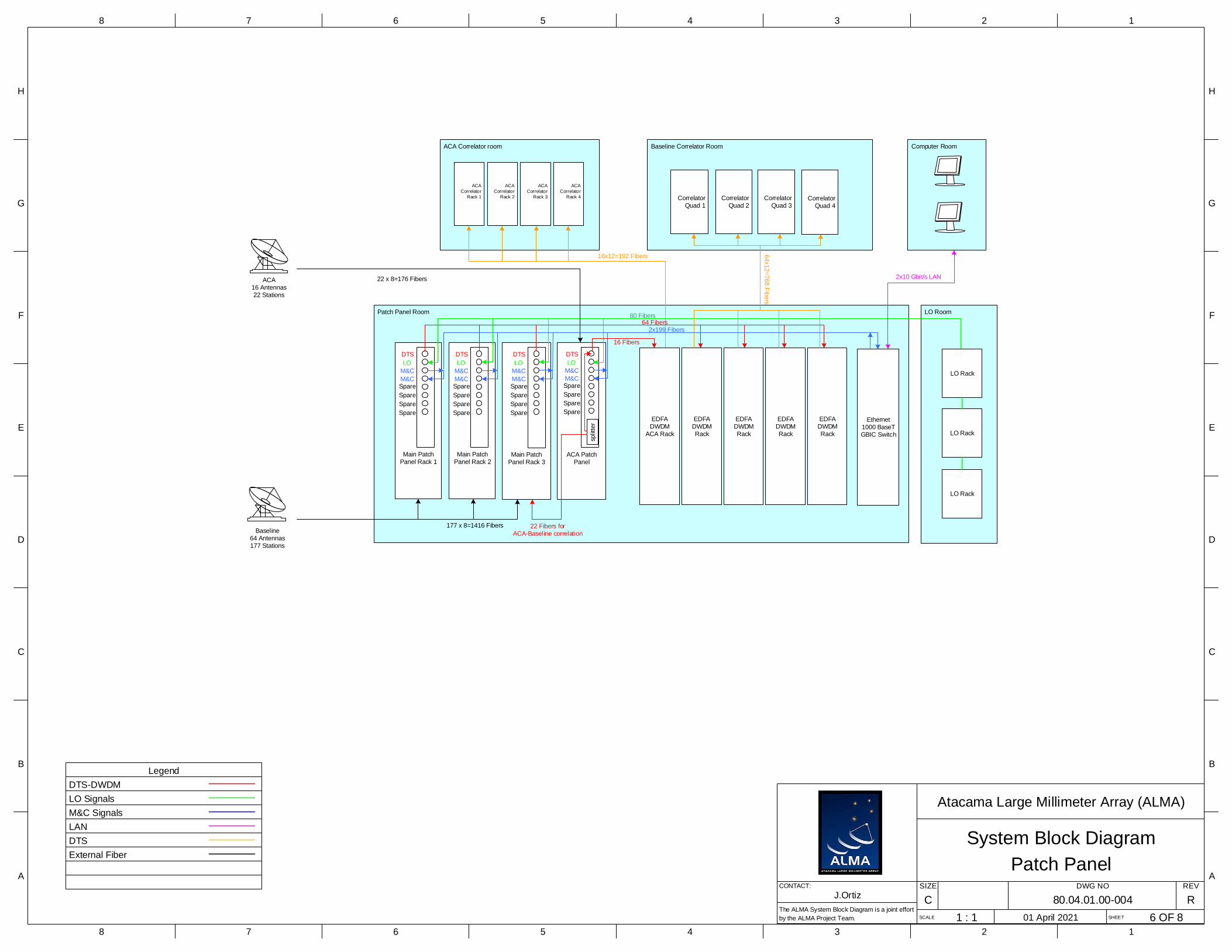
Patch Panel Room
Main Patch Panel Rack 2
LO Room
Computer Room
1664 fibers
ACA Correlator room
20
8 F
ibe
rs
Baseline64 Antennas177 Stations
ACA
Correlator
Rack 1
Main Patch Panel Rack 3
ACA Patch Panel
Baseline Correlator Room
CorrelatorQuad 1
CorrelatorQuad 2
CorrelatorQuad 3
CorrelatorQuad 4
splitter
EDFADWDM Rack
EDFA DWDM Rack
EDFA DWDM Rack
EDFA DWDM Rack
DTS
LO
M&C
M&CSpare
Spare
Spare
Spare
DTS
LO
M&C
M&CSpare
Spare
Spare
Spare
DTS
LO
M&C
M&CSpare
Spare
Spare
Spare
Ethernet 1000 BaseT GBIC Switch
LO Rack
22 x 8=176 Fibers
80 Fibers64 Fibers
2x199 Fibers
64x12=
768 F
ibers
16x12=192 Fibers
2x10 Gbit/s LAN
22 Fibers for ACA-Baseline correlation
split
ter
177 x 8=1416 Fibers
ACA
Correlator
Rack 4
ACA
Correlator
Rack 3
ACA
Correlator
Rack 2
EDFADWDM
ACA Rack
16 Fibers
Main Patch Panel Rack 1
DTS
LO
M&C
M&CSpare
Spare
Spare
Spare
LO Rack
LO Rack
ACA 16 Antennas22 Stations
DTS
External Fiber
LAN
Legend
DTS-DWDM
LO Signals
M&C SignalsAtacama Large Millimeter Array (ALMA)
System Block Diagram
Patch PanelSIZE DWG NO REV
C 80.04.01.00-004 R
SCALE 1 : 1 01 April 2021 SHEET 6 OF 8The ALMA System Block Diagram is a joint effort
by the ALMA Project Team.
CONTACT:
J.Ortiz

H
G
F
E
D
C
B
A
8 7 6 5 4 3 2 1
H
G
F
E
D
C
B
A
8 7 6 5 4 3 2 1
Atacama Large Millimeter Array (ALMA)
System Block Diagram
CLOA Rack Power Distribution and Control
SIZE DWG NO REV
C 80.04.01.00-004 R
SCALE 1 : 1 01 April 2021 SHEET 7 OF 8The ALMA System Block Diagram is a joint effort
by the ALMA Project Team.
CONTACT:
J.OrtizNote: The original drawing source is BEND-50.01.00.00-032-A-DWG, 08 August 2009, W.Grammer/E.Ford
H-MASER

H
G
F
E
D
C
B
A
8 7 6 5 4 3 2 1
H
G
F
E
D
C
B
A
8 7 6 5 4 3 2 1
Item Description References/comments
01 Wide Range Turbo molecular Pump
incl. Turbo-Drive “S”
Leybold TURBOVAC TW 70H
02 Diaphragm Pump Leybold DIVAC 2.5VT
03 Right Angle Valve Leybold 16KF
04 Cryostat Gate Valve Gate Valve VAT / (or optional
manual butterfly valve VAT)
05 Butterfly valve / lockable Alcatel
06 ITR90 wide range gauge head Leybold
07 ITR90 wide range gauge head (spare) Leybold
08 Center 2 Gauge Controller Leybold
09 Pressure switch Leybold TTR70
10 Electromagnetic valve Leybold
11 Self Sealing Quick Coupling Swagelok
12 Pressure reduction Air Liquide
13 Dry N2 reservoir Air Liquide
14 Proximity switch Baumer
15 Pressure Relieve valve RAL
16 Temp. Sensor Ultimate pressure
sensor
Pt-100/ Jumo
17 Vacuum Vessel -
18 Antenna cabin temperature sensor Pt-100/Jumo
19 - -
20 Three stage cold head Sumitomo RDK3ST-R2
21 ICCU/ Indoor Compressor and
Control Unit
Sumitomo part of CAN-61D
22 OCU/ Outdoor compressor unit Sumitomo CAN-61D
23 He-Buffer Tank Sumitomo
24 Pressure sensor (supply) Sumitomo
25 Pressure sensor (return) Sumitomo
26 Pressure sensor (He-Buffer Tank) Sumitomo
27 He-flex line (He-Buffer Tank – Cold
Head)
Sumitomo (1/4’Aero Quip) He-Pot
feed
28 He line between
ICCU/OCU(outdoor)
ALMA-40.03.02.06-003- A-DWG
29 He supply line (outdoor) ALMA-40.03.02.06-005- A-DWG
30 He return line (outdoor) ALMA-40.03.02.06-004- A-DWG
31 He return line (indoor) ALMA-40.03.02.06-006- A-DWG
32 He supply line (indoor) ALMA-40.03.02.06-007- A-DWG
Note: The original drawing source is SYSE-40.03.02.00-037-A-DWG, 08 February 2010, R. Hinters
Atacama Large Millimeter Array (ALMA)
System Block Diagram
Cryogenic/Vacuum SystemSIZE DWG NO REV
D 80.04.01.00-004 Q
SCALE 1 : 1 01 April 2021 SHEET 8 OF 8The ALMA System Block Diagram is a joint effort
by the ALMA Project Team.
CONTACT:
G. Siringo

OFL
MUX
From the PIC
deployed at AOS,
BL correlator
PIC X,Q1
PIC Y,Q1
PIC X,Q1
PIC X,Q2
PIC Y,Q2
PIC X,Q3
PIC Y,Q3
PIC X,Q4
PIC Y,Q4
VLBI recorder 1
Mark 6
VLBI recorder 2
Mark 6
VLBI recorder 3
Mark 6
VLBI recorder 4
Mark 6
PIC X,Q1
PIC Y,Q1
PIC X,Q2
PIC Y,Q2
PIC X,Q3
PIC Y,Q3
PIC X,Q4
PIC Y,Q4
Computing Room at the OSF