asic 121: practical vhdl digital design for fpgas tutorial 1 september 27, 2006
TRANSCRIPT
ASIC 121: Practical VHDL Digital Design for FPGAs
Tutorial 1
September 27, 2006
Contributions
• I have taken some of the slides in this tutorial from Jeff Wentworth’s ASIC 120
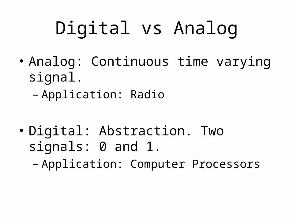
Digital vs Analog
• Analog: Continuous time varying signal.– Application: Radio
• Digital: Abstraction. Two signals: 0 and 1.– Application: Computer Processors
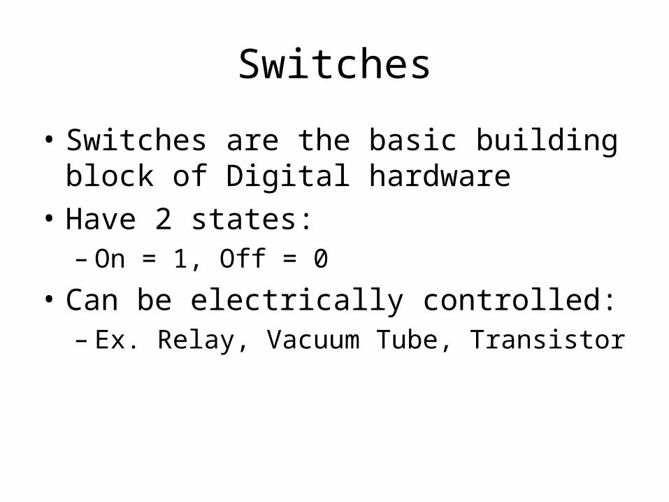
Switches
• Switches are the basic building block of Digital hardware
• Have 2 states:– On = 1, Off = 0
• Can be electrically controlled:– Ex. Relay, Vacuum Tube, Transistor
Transistor
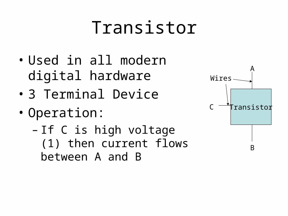
• Used in all modern digital hardware
• 3 Terminal Device
• Operation:– If C is high voltage (1) then
current flows between A and B
Transistor
A
B
C
Wires
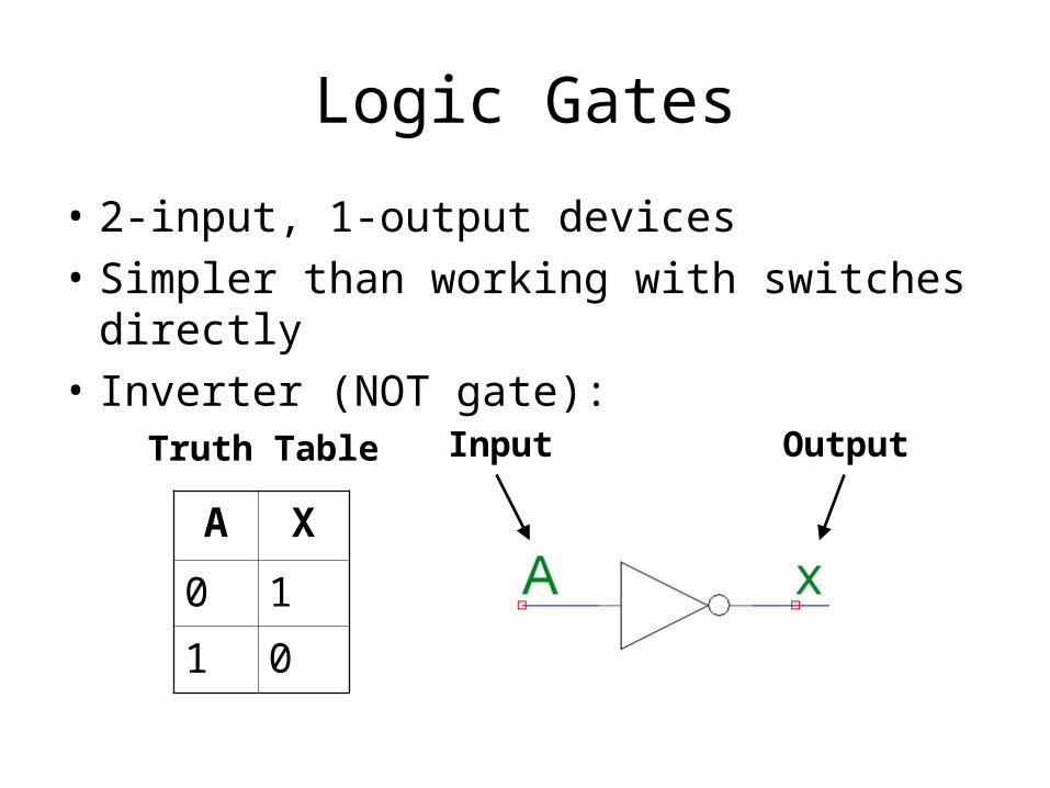
Logic Gates
• 2-input, 1-output devices
• Simpler than working with switches directly
• Inverter (NOT gate):
A X
0 1
1 0
Input OutputTruth Table
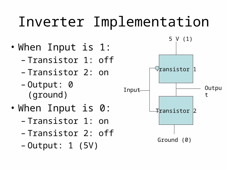
Inverter Implementation
• When Input is 1:– Transistor 1: off– Transistor 2: on– Output: 0 (ground)
• When Input is 0:– Transistor 1: on– Transistor 2: off – Output: 1 (5V)
Transistor 1
5 V (1)
Input Output
Transistor 2
Ground (0)
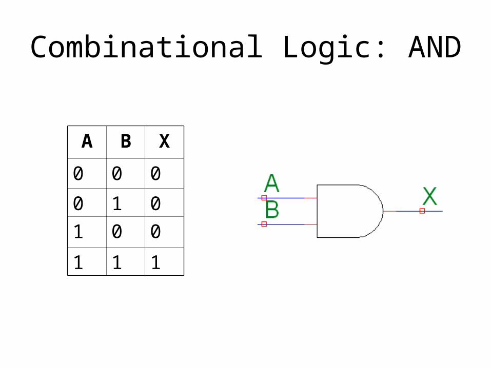
Combinational Logic: AND
A B X
0 0 0
0 1 0
1 0 0
1 1 1
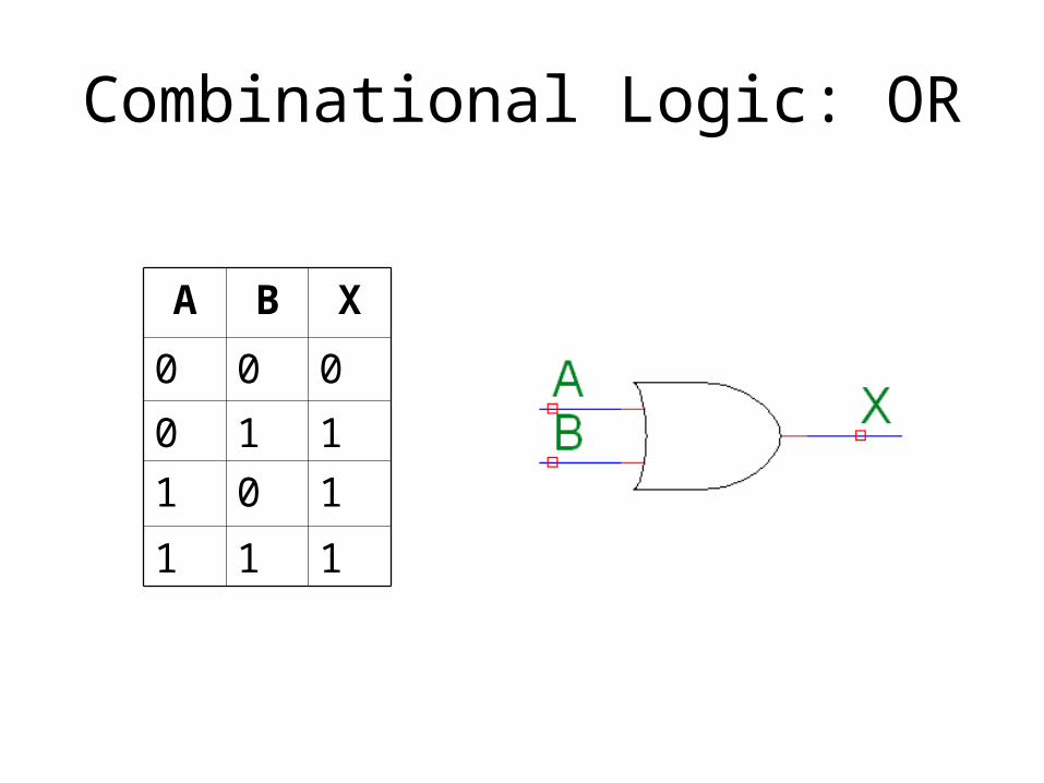
Combinational Logic: OR
A B X
0 0 0
0 1 1
1 0 1
1 1 1
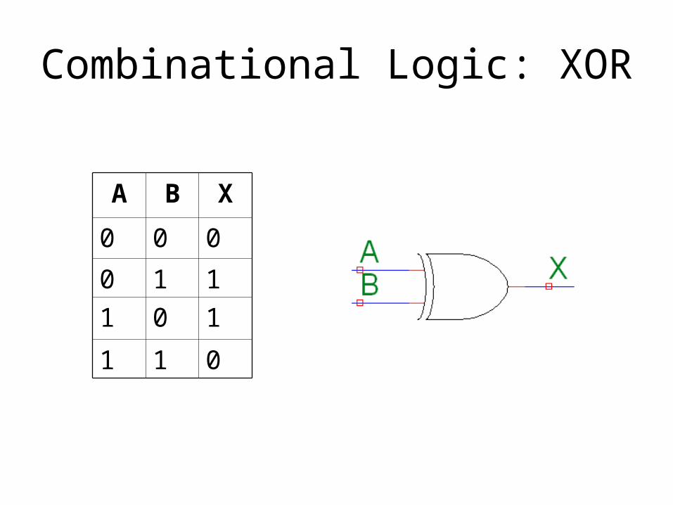
Combinational Logic: XOR
A B X
0 0 0
0 1 1
1 0 1
1 1 0
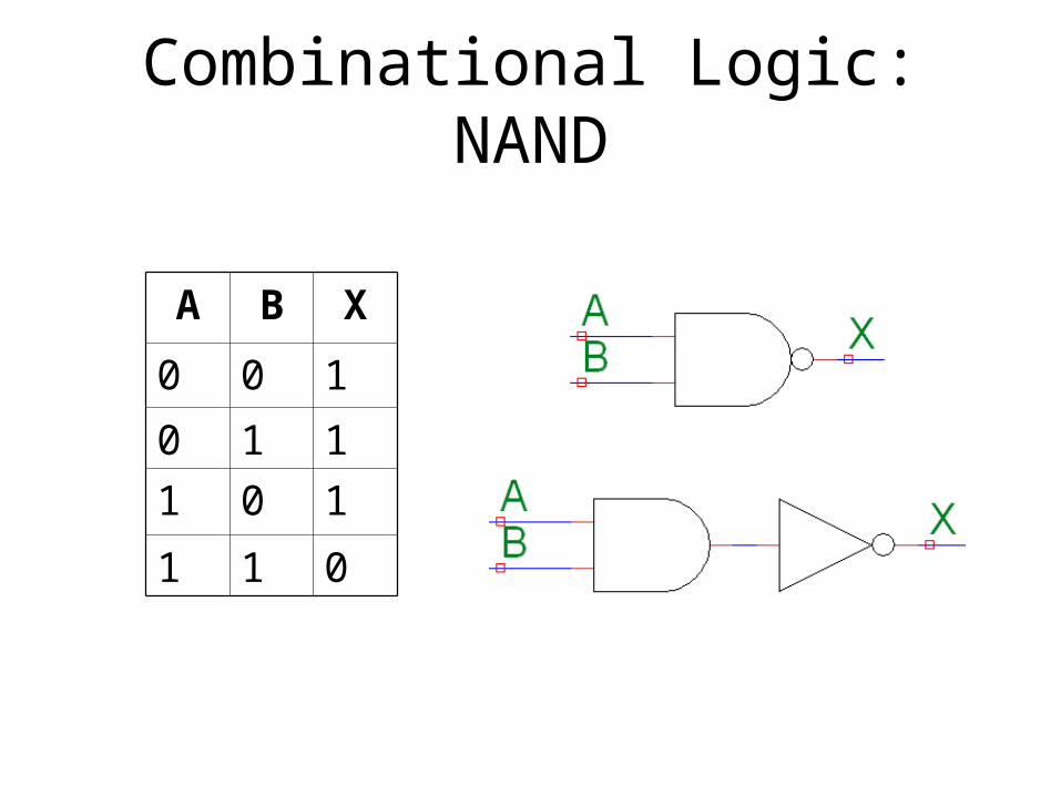
Combinational Logic: NAND
A B X
0 0 1
0 1 1
1 0 1
1 1 0

Combinational Logic: NOR, XNOR
A B X
0 0 1
0 1 0
1 0 0
1 1 0
A B X
0 0 1
0 1 0
1 0 0
1 1 1
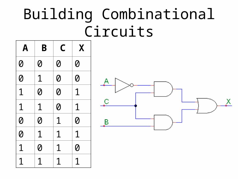
Building Combinational Circuits
A B C X
0 0 0 0
0 1 0 0
1 0 0 1
1 1 0 1
0 0 1 0
0 1 1 1
1 0 1 0
1 1 1 1
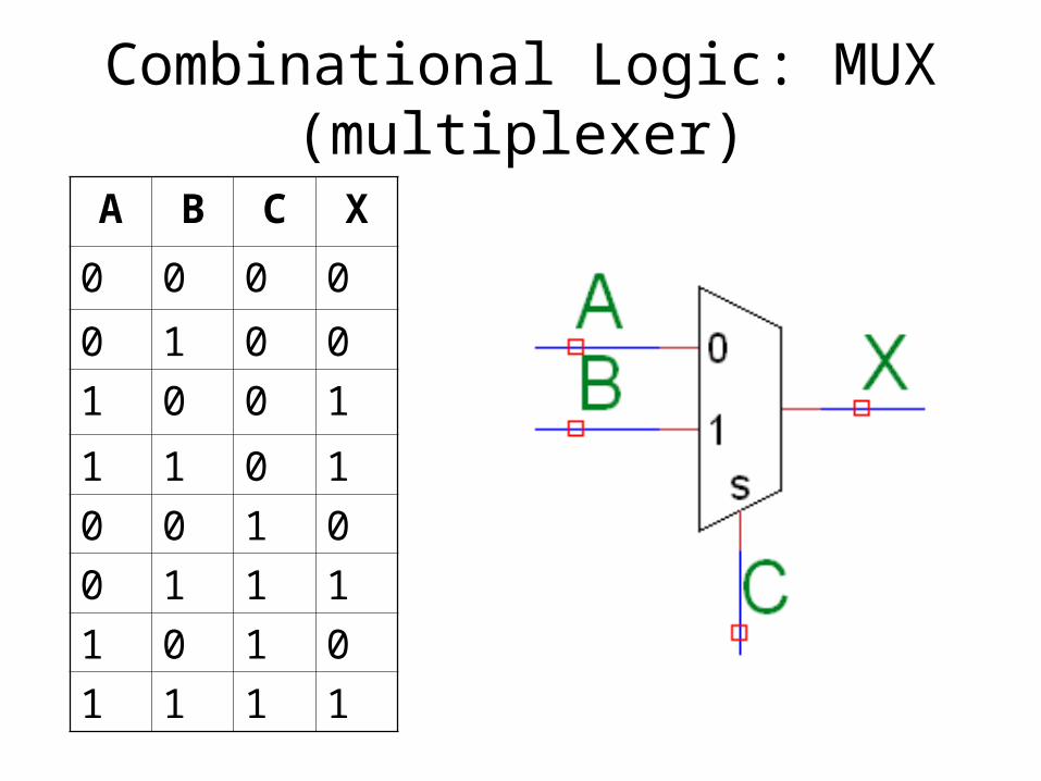
Combinational Logic: MUX(multiplexer)
A B C X
0 0 0 0
0 1 0 0
1 0 0 1
1 1 0 1
0 0 1 0
0 1 1 1
1 0 1 0
1 1 1 1
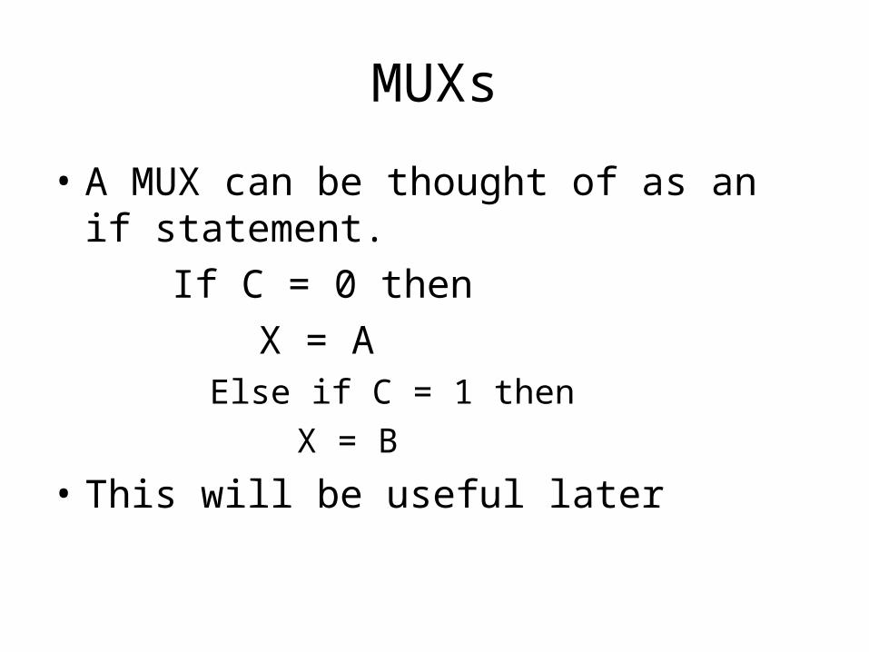
MUXs
• A MUX can be thought of as an if statement.
If C = 0 then
X = AElse if C = 1 then
X = B
• This will be useful later
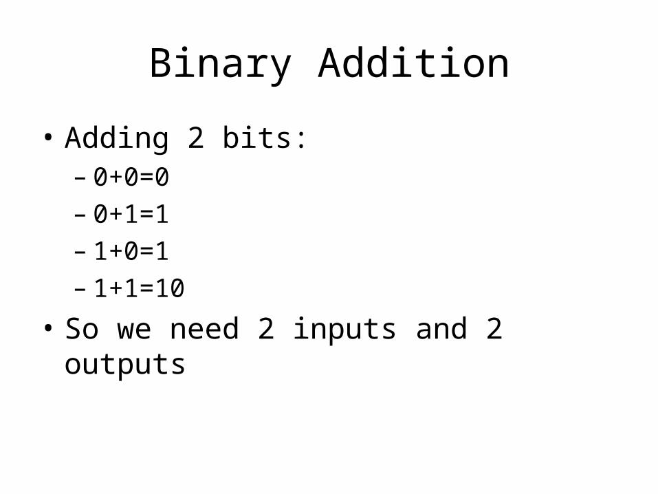
Binary Addition
• Adding 2 bits:– 0+0=0– 0+1=1– 1+0=1– 1+1=10
• So we need 2 inputs and 2 outputs
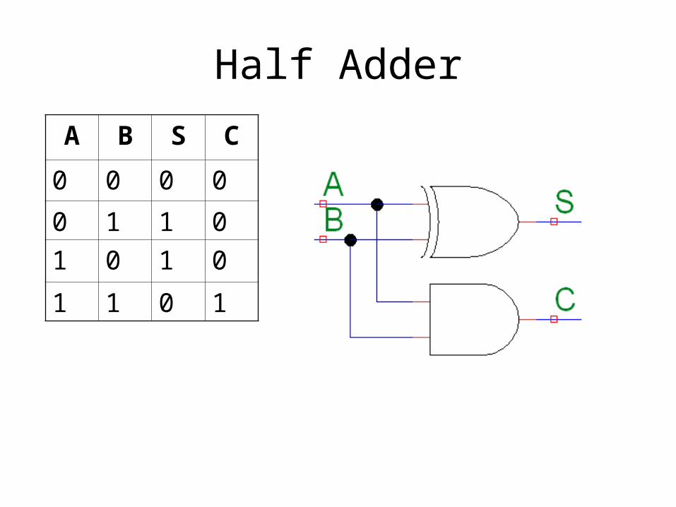
Half Adder
A B S C
0 0 0 0
0 1 1 0
1 0 1 0
1 1 0 1
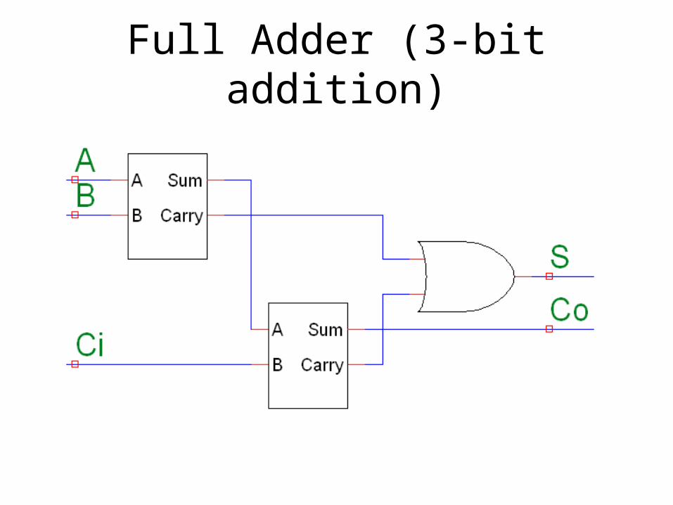
Full Adder (3-bit addition)
Independent Tasks
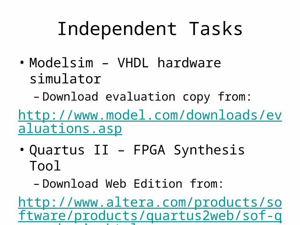
• Modelsim – VHDL hardware simulator– Download evaluation copy from:
http://www.model.com/downloads/evaluations.asp
• Quartus II – FPGA Synthesis Tool– Download Web Edition from:
http://www.altera.com/products/software/products/quartus2web/sof-quarwebmain.html
Development Boards
• For interested students there are development boards available
• Check out the DE2: http://www.altera.com/education/univ/materials/boards/unv-de2-board.html
• The DE2 comes with lab exercises and design examples
• Not cheap: $269 US
Quartus II Exercise
• Open Quartus II, Select File->New Project Wizard, Select a valid working directory (should be an empty folder)
• Name the project and entity “half_adder”
• Click next for all other menus
• Select File->New. Select VHDL File
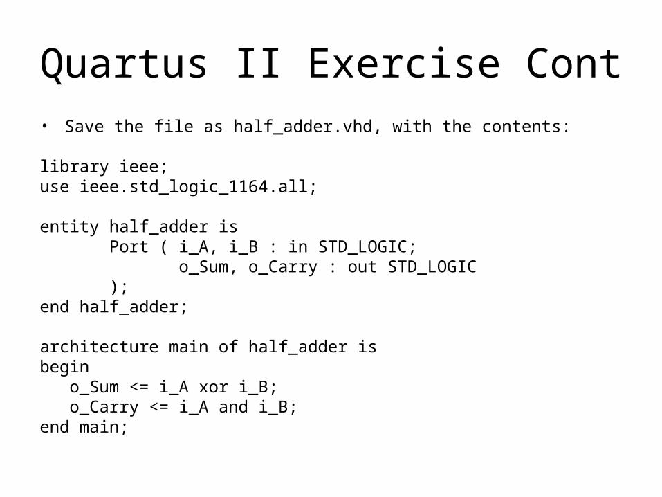
Quartus II Exercise Cont• Save the file as half_adder.vhd, with the contents:
library ieee;use ieee.std_logic_1164.all;
entity half_adder is Port ( i_A, i_B : in STD_LOGIC; o_Sum, o_Carry : out STD_LOGIC );end half_adder;
architecture main of half_adder isbegin o_Sum <= i_A xor i_B; o_Carry <= i_A and i_B;end main;
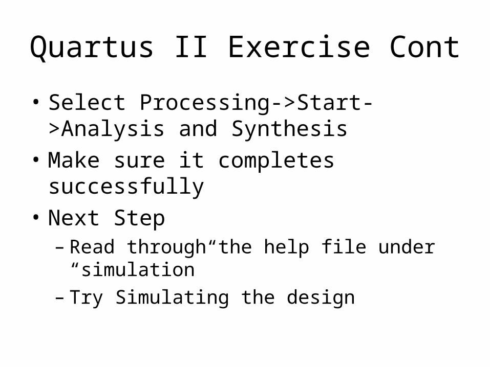
Quartus II Exercise Cont
• Select Processing->Start->Analysis and Synthesis
• Make sure it completes successfully
• Next Step– Read through the help file under “simulation”– Try Simulating the design