assembling the ece 4760 small dev board c1 100nf...
TRANSCRIPT

Assembling the ECE 4760 Small Dev Board
Bill of Materials
C1 100nF SMT
C2 100nF SMT
C3 10uF SMT
C4 1uF SMT
C5 1uF SMT
D1 1N4007 SMT
J1 ICSP HEADER (6 pin header-plug)
J2 Input Supply (2.1 mm Power input jack)
J3 Power Outputs
J4 PIC GPIO 1
J5 PIC GPIO 2 (NOTE: J3, J4, J5 will use one 28 pin header-plug)
R1 10k SMT
SW1 RESET (Toggle switch)
SW2 POWER (Button switch)
U1 PIC32MX250F128B (Use a 28-pin PDIP 0.3in socket)
U2 MCP1702
Off board: 5v AC adapter (wall wart)
Note:
For ease of reference, we shall refer to the directions of the board with north being the edge of the board with J1, south the edge with all GPIO pins, east with the power input, and west with R1. As you are assembling the board, refer to the attached pictures for reference points.
Recommended assembly procedure:
1. Solder the surface mount (SMT) parts onto the board. This includes: R1, C1, C2, C3, C4, C5, D1. For D1, the thin white line on the top of the part indicates the cathode end of the diode, and should be placed such that the line is closest to the north edge.
2. Solder the toggle switch at SW2, orientation is not important. When this is done, when the switch is in the north position, the circuit is complete and the board is considered powered on. When in the south position, the circuit is broken, and the board is considered powered off.

3. Solder the 2.1 mm power input jack at J2, such that the power socket opening is directly facing the east edge of the board. Note: the through holes are much larger than the pins due to the peculiar shape of the pins. It will require much solder to make a solid connection all around the pin and the surrounding through hole.
4. Solder the MCP1702 into U2. Refer to the pinout diagram to the right. As a rule of thumb, when looking directly down on the board with the north edge at the top of your field of vision, the top of the MCP1702 device will resemble the letter ‘D’.
5. STOP soldering for a moment and check the power circuit before continuing. With the toggle switch in the off position, connect a power supply to the power input jack using an appropriate plug. It is recommended to use a 5v AC adapter, but the circuit will theoretically operate with up to a 12v AC adapter. Move the switch to the on position. If anything begins to burn, smoke, or heat up dangerously, immediately switch off power and unplug the adapter. You will need to recheck your connections and orientations of the soldered devices. If nothing appears wrong, using a multimeter, check the voltage across the +3.3V through holes and the GND through holes on the south edge of the board on the east side. If you read a positive 3 volt difference, you may continue assembling the board after unplugging and powering off. If not, recheck your connections and orientations of the soldered devices after unplugging and powering off.
6. Take the button switch intended for SW1, and with a pair of pliers, gently straighten the leads, until the device easily fits in the SW1 through holes. Orientation is not important. Solder the device.
7. Solder the PDIP socket in the U1 place for the PIC to eventually go into. Orientation of the socket is not important. There is often a dent or indent in the pin 1 end, and this should face the west side of the board.
8. You may want to skip this step, if you intend to connect wires, or you may want to orient the pins upward, rather than below the board. The following assumes that you want the pins oriented downward. Place the 28-pin header-plug into the GPIO/power through holes, such that the shorter side of the metal enters the holes from the underside of the board, such that the black spacers are on the bottom of the board, with the longer metal side of the headers pointing out of the bottom of the board. Solder this header in place by soldering the top of the board. See pictures if further clarification is needed.
9. Doing the opposite for the 6-pin header-plug into J1, solder it in place such that the longer side of the metal headers and the black spacers are on the top of the board, and the solder points are on the bottom of the board. See pictures if further clarification is needed.
10. Place the PIC32 into the PDIP socket, such that the notch on the device points toward the west edge of the board.
11. Plug in the AC adapter, power on and begin testing.
NOTE: The PICkit 3 programmer goes on the board with the lighted side facing north. See appendix for pictures. The Microstick programmer is connected as shown on the development board page.
Appendix: Pictures
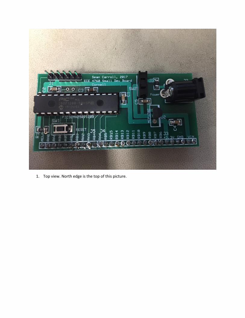
1. Top view. North edge is the top of this picture.

2. Side view from south edge.
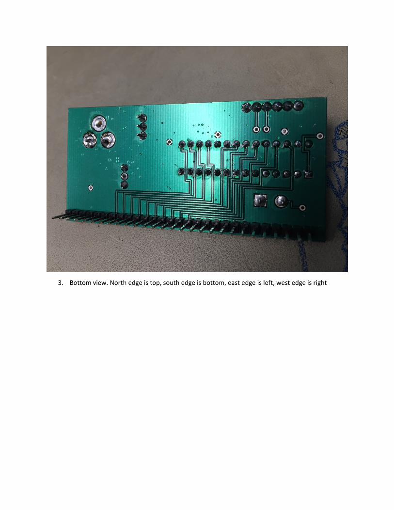
3. Bottom view. North edge is top, south edge is bottom, east edge is left, west edge is right

4. Same bottom view as 3, different angle.
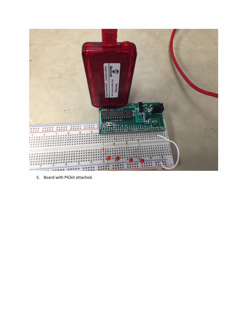
5. Board with PICkit attached.
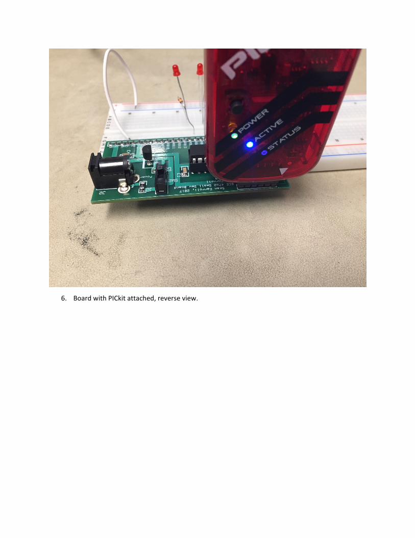
6. Board with PICkit attached, reverse view.