assembly and test houses: requirements for … · discrete semiconductor technologies basic...
TRANSCRIPT
DLR-RF-PS-STD-009
Issue 1
April 2010
Assembly and Test Houses:
Requirements for Capability Approval of
Discrete Semiconductor Technologies
Basic Specification No.2435200
Issue 1
Deutsches Zentrum German für Luft- und Raumfahrt e.V. Aerospace Center
Assembly and Test Houses:
Requirements for Capability Approval of Discrete Semiconductor Technologies Basic Specification No.2435200
DLR-RF-PS-STD-009
2
Copyright © 2005 German Aerospace Center - DLR. All rights reserved. Copyright © in this document is owned by German Aerospace Center - DLR. Any person is hereby authorized to view, copy, print, and distribute this document subject to the following conditions:
The document may be used for informational purposes only. The document may only be used for non-commercial, non-profit purposes. Any copy of this document thereof must include this Copyright notice.
This document is provided "as is", and copyright holders make no warranties, including, but not limited to, warranties of merchantability, fitness for a particular purpose, non.infringement; that the contents of the document are suitable for any purpose; nor that the implementation of such contents will not infringe any third party patents, copyrights, trademarks or other rights. Copyright holders will not be liable for any direct, indirect, special or consequential damages arising out of any use of the document or the performance or implementation of the contents thereof. For permission requests, questions, or further information, please contact Dr. Andreas Jain - DLR - Quality and Product Assurance, +49 (2203) 601 - 2954.
Assembly and Test Houses:
Requirements for Capability Approval of Discrete Semiconductor Technologies Basic Specification No.2435200
DLR-RF-PS-STD-009
4
TABLE OF CONTENTS
1. PURPOSE............................................................................................................. 6
2. APPLICABLE DOCUMENTS................................................................................ 6
3. TERMS, DEFINITIONS, ABBREVIATIONS, SYMBOLS AND UNITS................... 6
4. INTRODUCTION................................................................................................... 7
4.1 GENERAL ............................................................................................................. 7 4.2 CAPABILITY PROGRAM VARIANTS.................................................................... 7
5. EVALUATION OF MANUFACTURER .................................................................. 8
6. DEFINITION OF CAPABILITY DOMAIN AND BOUNDARIES ............................. 8
6.1 GENERAL ............................................................................................................. 8 6.2 PROCESS IDENTIFICATION DOCUMENT (PID) ................................................. 8 6.3 PHYSICAL DESIGN.............................................................................................. 9 6.4 DESIGN SYSTEM................................................................................................. 9 6.5 WAFER/CHIP FABRICATION PROCESSES ...................................................... 10 6.6 PROCUREMENT OF WAFER/DIE...................................................................... 11 6.7 PACKAGE........................................................................................................... 12 6.8 ASSEMBLY PROCESSES .................................................................................. 12 6.9 TEST FACILITY .................................................................................................. 13 6.10 TRACEABILITY................................................................................................... 14
7. TEST SAMPLES AND MEASUREMENT METHODS ......................................... 14
7.1 GENERAL ........................................................................................................... 14 7.2 PROCESS AND DEVICE CHARACTERISTICS.................................................. 14 7.3 DESIGN AND LAYOUT RULES .......................................................................... 15 7.4 DEVICE PERFORMANCE .................................................................................. 15 7.5 DEVICE RELlABlLITY INCLUDING RADIATION TOLERANCE .......................... 15 7.6 TECHNOLOGY ................................................................................................... 15 7.7 TEST DICE.......................................................................................................... 15
8. EVALUATION OF CAPABILITY DOMAIN.......................................................... 16
9. CAPABLLITY APPROVAL TESTING................................................................. 16
9.1 GENERAL ........................................................................................................... 16 9.2 CAPABlLITY APPROVAL TEST REPORT .......................................................... 16
10. COMPONENT TYPE APPROVAL TEST ............................................................ 16
11. REDUCTION. EXTENSION AND CHANGE OF THE CAPABLLITY DOMAIN ... 17
12. PROCUREMENT ................................................................................................ 17
CHART I - CAPABILTY APPROVAL TESTING ............................................................... 18
Assembly and Test Houses:
Requirements for Capability Approval of Discrete Semiconductor Technologies Basic Specification No.2435200
DLR-RF-PS-STD-009
5
Change Record
Issue Details of Change
A Initial Issue
Assembly and Test Houses:
Requirements for Capability Approval of Discrete Semiconductor Technologies Basic Specification No.2435200
DLR-RF-PS-STD-009
6
1. PURPOSE
This specification defines the requirements for Capability Approval of Discrete Semiconductor Technologies assembled and tested by Assembly and Test Houses (ATH). It outlines the requirements for the definition of the Capability Domain and its Boundaries, the Evaluation of a Capability Domain, Capability Approval Testing and Component Type Approval testing. ESCC Basic Specification No. 24300 gives the general requirements for Capability Approval of electronic component technologies.
2. APPLICABLE DOCUMENTS
The following specifications form part of, and shall be read in conjunction with, this specification. The relevant issues shall be those in effect at the date of commencement of the Capability Approval. DLR-Documents: - DLR No. 2025200, Checklist for Discrete Semiconductor Assembly and Test House and Line Survey; Basic Specification. - DLR No. 2265200, Evaluation Test Program for Discrete Semiconductor Devices assembled and tested in Assembly and Test House; Basic Specification. - DLR No. 5200, Discrete Semiconductor Components, Hermetically Sealed; Generic Specification. - DLR No. 5200/XXX, Discrete Semiconductor Component, Hermetically Sealed; Detail Specification for the relevant type respectively technologies. ESCC-Documents: - ESCC No. 20200, Component Manufacturer Evaluation; Basic specification. - ESCC No. 21300, Terms, Definitions, Abbreviations, Symbols and Units; Basic specification. - ESCC No. 21500, Calibration System Requirements; Basic specification. - ESCC No. 22600, Requirements for the Evaluation of Standard Electronic Components for Space Application; Basic specification. - ESCC No. 22700, Requirements and Guidelines for the Process Identification Document (PID); Basic specification. - ESCC No. 24300, Requirements for the Capability Approval of Electronic Component Technologies for Space Application; Basic specification. - ESCC No. 24600, Minimum Quality System Requirements; Basic specification.
3. TERMS, DEFINITIONS, ABBREVIATIONS, SYMBOLS AND UNITS
The terms, definitions, abbreviations, symbols and units in ESCC Basic Specification No. 21300 shall apply. In addition, the following shall apply: Abbreviations ATH Assembly and Test House DLR Deutsches Zentrum für Luft- und Raumfahrt ESCC European Space Component Coordination PID Parts Identification Document
Assembly and Test Houses:
Requirements for Capability Approval of Discrete Semiconductor Technologies Basic Specification No.2435200
DLR-RF-PS-STD-009
7
Definitions Assembly and Test House A company which procures the Discrete Semiconductor Chips
from the semiconductor manufacturer in the needed quality and at agreed standards, assembles these chips into packages and performs all relevant and required inspections, testing and measurements at chip and package level.
Semiconductor Manufacturer A company which designs the Discrete Semiconductor Chips,
develops the processes for the Chip Fabrication and performs the Chips Production in the required characteristic and quality.
4. INTRODUCTION
4.1 GENERAL
Capability Approval is the status granted to a manufacturer for a specified capability domain after successful completion of an evaluation and capability approval programme as defined herein. The programme consists of four phases: (a) Evaluation of manufacturer (b) Definition of the capability domain and its boundaries (c) Evaluation of the capability domain (d) Capability and type approval testing
4.2 CAPABILITY PROGRAM VARIANTS
As subsequent described this specification defines for Assembly and Test Houses (ATH) two variants of capability program. ATH Product Capability Approval The ATH Product Capability Approval of a component technology demands that all requirements for a component technology including the semiconductor chip technology are successful met. This requires in addition to the activities for the assembly and testing of the components at the ATH a very close cooperation with and control by the ATH of the semiconductor manufacturer and the willingness of the semiconductor manufacturer to perform all specified activities within this specification and in the specification ESCC 24300. After successful completion of the evaluation and capability approval program components within the specified capability domain are considered as qualified components. ATH Capability Approval The ATH Capability Approval requires the successful performance of all activities by the ATH for the assembly and testing of the components as specified within this specification and in the specification ESCC 24300. The ATH has to procure the semiconductor chips to the highest available quality level and has to demonstrate the compatibility of the semiconductor chips with the package and the applied assembly and testing processes. But the semiconductor manufacturer with his product is not part of the capability program. However, components delivered by a ATH with a ATH Capability Approval can not be considered as a qualified component. As long as these components are within the specified capability domain ( see paragraph 6 of this specification) only the assembly and the testing of such components can be considered as qualified.
Assembly and Test Houses:
Requirements for Capability Approval of Discrete Semiconductor Technologies Basic Specification No.2435200
DLR-RF-PS-STD-009
8
5. EVALUATION OF MANUFACTURER
The evaluation of the manufacturer is an exercise designed to assess the adequacy of the organisation, plant and facilities and the manufacturer’s fitness to provide electronic components suitable for space application. The exercise for the ATH shall be performed by the DLR in accordance with the requirements of ESCC No. 20200 and with the more detailed requirements given in DLR No. 2025200. In addition for the ATH Product Capability Approval the ATH has under the supervision of DLR to perform a similar exercise for assessing the semiconductor manufacturer’s fitness to supply the semiconductor wafers/chips for space application. The requirements for this exercise have to be tailored by the ATH for the individual case in accordance with the requirements given in DLR No. 2025200.
6. DEFINITION OF CAPABILITY DOMAIN AND BOUNDARIES
6.1 GENERAL
The ATH shall define the capability domain. This capability domain has to describe in a comprehensive manner in details the scope and extent of for which capability approval is sought in terms of the boundaries of technologies, performance, construction rules, design data, assembly processes and materials, packages, in-process testing and controls, the plant or plants were the processes are to be carried out etc. The definition shall clearly delineate all necessary boundaries, such that there can be no uncertainties regarding the extent what is to be qualified and deciding whether specific component types will be covered. The definition document shall be submitted to the DLR for approval prior to the start of the evaluation activities. It shall be updated, as necessary, during the course of the evaluation and capability approval testing. In case of a ATH Product Capability Program as defined in paragraph 4.2 above all of the subsequent required details of the semiconductor chip technology has to be included in the capability domain description. The definition has to comprise the areas listed in the following paragraphs at least to the extent detailed herein. Additional information has to be supplied, whenever necessitated by the particular nature of the technology under approval. In case anyone of the characteristics in the following paragraphs should not apply to the technology and/or methodology under approval, this shall be stated. For a ATH Capability Program only these criteria have to be specified of the semiconductor chip technology in the domain description, which are needed to be known for the appropriate selection and procurement of the chips and the packages and the correct application of the assembly and testing processes at the ATH. Furthermore, also the parameters of the chip technology, which can affect the parts performance and reliability by the assembly and testing processes, have to be defined in the capability domain.
6.2 PROCESS IDENTIFICATION DOCUMENT (PID)
The Capability Domain to be qualified shall also form the basis of the PID which has to be prepared by the ATH to the satisfaction of DLR. In terms of content and configuration control, the PID shall fulfil the requirements of ESCC Basic Specification No. 22700. It shall be updated, as necessary, during the course of the Capability exercise such that at the completion of Capability Approval accurately identifies all the processes used in the specified Domain. In preparing the PID the ATH may use extensive references to in-house documentation describing the processes as long as the relevant issues are clearly identified and subject to an acceptable control system.
Assembly and Test Houses:
Requirements for Capability Approval of Discrete Semiconductor Technologies Basic Specification No.2435200
DLR-RF-PS-STD-009
9
6.3 PHYSICAL DESIGN
The physical design is governed by a set of technology specific rules and parameters, commonly called “Design Rules”. These rules define the construction and composition of all structures foreseen for the design and manufacture of a semiconductor in a specific technology. The description of the physical design requires the definition of at least the following characteristic for ATH Product Capability Program and for the ATH Capability Program as relevant: ● Layout rules which specifies the topology of all physical structures, including those for
alignment and test purposes in terms of:
Function (e.g. diffusion, conductor, contact, dielectric….), Shape (e.g. ratios, angles….), Size (e.g. minimum/maximum width/length/depth…), Positioning (e.g. overlaps of compound structures, spacing between structures of
equal or different nature), Vertical dimensions of all layers (e.g. depth of diffusion, trenches; thickness of
polysilicon, metalisation…), Radiation hardness assurance considerations, if applicable.
● Electrical rules and parameters in terms of:
Sheet resistivities of layers used for resistors, Current carrying capability of conductive layers, Sheet and edge capacitances Dielectric breakdown voltages, Device parameters and associated simulation models,
If needed, other relevant parameters or restrictions not covered in the previous points shall also be stated.
6.4 DESIGN SYSTEM
The design methodology is defined by the design system and all other procedures applied in the design of a semiconductor. The design system comprises all software, basic design data and hardware platform. A ATH Product Capability Program of a design system requires the following as a minimum and a ATH Capability Program the information which are relevant: ● The implementation of a configuration control system guaranteeing the traceability of all
software and data forming part of the system and ● The application of a quality assurance system addressing at least documentation procedures,
acceptance testing prior to system release and the organisation of error reporting and corrective action procedures.
Both systems shall be fully documented and their application has to be evident.
At least the following items shall be covered in the domain description:
● A general description of the design system representing:
The design flow.
The data flow within the system.
Assembly and Test Houses:
Requirements for Capability Approval of Discrete Semiconductor Technologies Basic Specification No.2435200
DLR-RF-PS-STD-009
10
● All relevant electrical and timing parameters including the power consumption.
● The final layout after completion of all post processing steps.
● A description of the hardware platform (e.g. work stations).
● Software and associated data shall be described in terms of :
The origin and version of the programme.
A comprehensive description of its functional scope.
The programming language.
The memory requirement.
Definition of data formats and description languages.
Definition of programme interfaces.
A description of the human interface with admitted or required interactivity and output format.
All software serving simulation type purposes requires a detailed description of the underlying models and their parametric capability.
6.5 WAFER/CHIP FABRICATION PROCESSES
The wafer/chip fabrication processes to be covered by the description should include, but not be limited, for ATH Product Capability Program to the following areas and for the ATH Capability Program only to these criteria which have to be known for an appropriate assembly process and which can be affected by the assembly and testing: ● Fabrication process sequence and limits. ● Fabrication process materials and materials specifications. ● Quality control and incoming inspection of materials and piece parts. ● Traceability and control of stored materials, especially limited shelf life items. ● Photoresistive materials and material specifications. ● Method of mask generation and identification. ● Doping material source, concentration and process technique. ● Cross section diffusion profile. ● Passivation or glassivation material, thickness and technique. ● Passivation and glassivation process temperature and time. ● Oxidation process, oxide composition and thickness, oxidation temperature and time. ● Metalisation system (pattern, material, deposition and etching technique, line width and
thickness). ● Gate formation process, material and technique. ● Conductor and dielectric materials. ● Ohmic contact formation. ● Backside process including wafer thinning and backside metalisation. ● Sintering and annealing temperature and time. ● Parameter monitor and how it is tested. ● Sample plans (quantity and acceptance numbers) ● Probing. ● Wafer acceptance criteria. ● Wafer handling and storage conditions. ● Lot formation. ● Cleanroom conditions. ● Material qualification. ● Physical location of wafer fabrication line.
Assembly and Test Houses:
Requirements for Capability Approval of Discrete Semiconductor Technologies Basic Specification No.2435200
DLR-RF-PS-STD-009
11
6.6 PROCUREMENT OF WAFER/DIE
The relationship and interface between wafer/die manufacturer and the ATH and the tools for the procurement of the wafer/die from the semiconductor manufacturer are the key elements of the ability of the ATH to assemble, package, test and deliver discrete semiconductor devices suitable for space applications. For the ATH Product Capability Program, this interface has to comprise the subsequent primary elements applicable to the claimed capability: The following elements are also very important for the ATH Capability Program. But due to the missing cooperation of the semiconductor manufacturer in the capability approval program not all of the subsequent information may be obtained by the ATH. For the not available information from the semiconductor manufacturer corresponding statements, why the information can not provided, have to be made in the in the Capability Domain Description. ● Identification of wafer/die source and procured technology.
Detail of source(s), identity, location and points of contact. Type of source (e.g. Fabrication plant, authorised distributor). Procured technology. Quality status of procured wafer/die
● Statement of the relationship between the semiconductor manufacturer and the ATH.
Formalised authority from the semiconductor manufacturer for the delivery of wafers/chips and their assembly, packaging and testing and distribution to the market.
Details of contractually binding agreement with the semiconductor manufacturer. Discussion/ agreement with the wafer/die manufacturer concerning intended use,
assembly, packaging and test methods. Agreements and liabilities relating to failures during assembly, packaging and testing. Agreements and liabilities relating to “in service” failures as a result of problems with
the procured wafer/die. Configuration management and change control arrangements, notification of
changes in semiconductor fabrication process and semiconductor design. Notification by the semiconductor manufacturer of problems and fabrication
deficiencies found subsequently to delivery of wafer/die.
● Control of the wafer/die source
Wafer/die design, technology and/or process changes. Production yield over time. Quality of the delivered wafer/die. Performance characteristic of the delivered wafer/die.
● Wafer/die procurement specification
Form and content of procurement specification including the definition of design,
technology, materials, processes, quality and performance characteristic of the wafer/die.
● Incoming inspection of procured wafer/die
The documentation, procedures and facilities used for the inspection of procured
wafer/die. Procedures used for checking compliance with wafer/die procurement specifications. Control of delivery data with wafer/die for assuring lot traceability and homogeneity. Verification of the mountability and bondability of the delivered chips.
Assembly and Test Houses:
Requirements for Capability Approval of Discrete Semiconductor Technologies Basic Specification No.2435200
DLR-RF-PS-STD-009
12
6.7 PACKAGE
For both variants, the ATH Product Capability Program and the ATH Capability Program, the package characteristic to be covered by the domain description should include, but not limited to the following areas:
● Package Vendor.
● External dimensions.
● Cavity dimensions.
● Body material.
● Body plating material.
● Body plating thickness.
● Bond pad material.
● Bond pad plating.
● Bond pad plating thickness.
● Lid material.
● Lid plating materials.
● Lid plating thickness.
● Lid seal (perform) material.
● Lid glass seal material.
● Lid glass seal thickness.
● Number of leads or terminals.
● Lead or terminal dimensions.
● Lead or terminal base material.
● Lead or terminal plating material.
● Lead attachment.
● Lead glass seal material.
● Lead glass seal thickness.
● Leads or terminals spacing.
● Lead configuration.
● Maximum allowable die size.
● Device marking process.
● Procurement Specification.
● Lot size.
● Procedure for incoming inspection at ATH.
6.8 ASSEMBLY PROCESSES
The assembly processes to be covered by the domain description should include, but not be limited to, the following areas for both variants the ATH Product Capability Program and the ATH Capability Program:
Assembly and Test Houses:
Requirements for Capability Approval of Discrete Semiconductor Technologies Basic Specification No.2435200
DLR-RF-PS-STD-009
13
● Scribing and die separation method (dicing of wafer).
● Die size.
● Assembly flow.
● Die back surface preparation.
● Die attach material, method and location.
● Bond pad geometry, spacing and metalisation.
● Wire/ribbon bond interconnect method.
● Moulding material and method of application, if applicable.
● Seal technique (material, sealing process and gas composition).
● Internal water vapour control program.
● Selection and specification of assembly materials.
● Quality control of incoming materials.
● Periodic test and inspection procedures.
● Implementation procedure for internal and other test methods.
● Sample plans (quantities and acceptance numbers).
● Traceability and control of stored materials, especially limited shelf life items.
● Physical location of assembly operation.
● Screening tests.
● Device marking process.
● Lot formation.
6.9 TEST FACILITY
For a ATH Product Capability Program and for a ATH Capability Program the domain description of the test facility requires the definition of at least the following areas:
● Implementation procedures for visual inspection and other test methods.
● Testing flow.
● Sample plans (quantity and acceptance numbers)
● Test procedures.
● Lot formation.
● Physical location of test facility.
The ATH shall describe inspection and test methods giving references to the documents specifying the methods. For a ATH Product Capability Program and for a ATH Capability Program the following areas shall be covered as a minimum:
● In-process inspection.
● Wafer acceptance testing.
● Incoming inspection.
● Precap inspection.
● Screening and associated electrical tests.
● Capability approval testing.
● Lot Acceptance testing.
Assembly and Test Houses:
Requirements for Capability Approval of Discrete Semiconductor Technologies Basic Specification No.2435200
DLR-RF-PS-STD-009
14
6.10 TRACEABILITY
A traceability system must be defined which includes the maintenance of records which allow traceability from the device serial number to the specific used materials, applied processes and performed inspections on the wafer lot and the assembly activities and where relevant, to a specific wafer for parts where any testing ( e.g. irradiation testing) is performed on a wafer by wafer basis. The ATH shall describe in the domain description for both variants the methods for assuring traceability of materials and components. For the ATH Product Capability Program the traceability system has to cover both the wafer/chip and the assembly processes. For the ATH Capability Program at least the traceability information of the assembly processes including all data from the wafer/chip procurement have to be maintained.
7. TEST SAMPLES AND MEASUREMENT METHODS
7.1 GENERAL
For a ATH Product Capability Program Test samples which are required for evaluation, Capability Approval Testing and process control shall be described in the PID and shall be produced strictly according to this document. Production and screening shall be to the highest quality level specified in the PID. Test samples shall be from different locations on the wafer or where appropriate, from different locations of the wafers in a wafer lot. The description of the test samples within the PID shall include the required test and/or measurement methods to be applied at wafer and/or at chip level and where these tests and/or measurements are performed. The ATH shall define in the PID the acquisition and maintenance of traceability to data occurred from test samples that establish the characterization of:
● Process and device characteristics (para. 7.2)
● Design and layout rules (para. 7.3)
● Device performance (para. 7.4)
● Device reliability (para. 7.5)
● Other relevant parameters for test and production devices. For a ATH Capability Program with high probability only wafer/die with limited data can be procured. The ATH shall define in the PID the acquisition, the quality level and maintenance of traceability of the wafer/chip required for evaluation, capability approval testing and process control. With the procurement of these wafers/chips at least the data should be collected from the semiconductor manufacturer or obtained by test and measurements at the ATH which are specified in the domain description of the ATH Capability Program . These are the parameters to be known for the appropriate selection and procurement of the chips and the packages and the appropriate assembly and testing processes at the ATH. Furthermore, these are also the parameters of the chip technology, which can be affected by the assembly and testing processes at the ATH. The data are necessary to provide the demonstration that the quality and reliability of wafer/die is equal to and commensurate with that of the wafer/die delivered later by the semiconductor manufacturer for the space parts.
7.2 PROCESS AND DEVICE CHARACTERISTICS
Test samples shall be provided to verify all relevant material, process and device parameters such as those listed below :
● Carrier mobilities.
Assembly and Test Houses:
Requirements for Capability Approval of Discrete Semiconductor Technologies Basic Specification No.2435200
DLR-RF-PS-STD-009
15
● Crystalline defects in the semiconductor material.
● Doping profiles.
● Junction alignment.
● Sheet resistance for each no dielectric layer e.g. diffused or implanted regions, polysilicon metal or other .
● Dielectric isolation (breakdown voltage).
● Actual line widths.
● Interface properties.
● Device parameters
● Leakage currents.
● Wire bonding.
● Die bonding.
7.3 DESIGN AND LAYOUT RULES
Test samples shall be provided to verify the geometrical layout rule set as defined in the domain description and to allow electrical or optical evaluation of layer-to-layer misalignment which might occur during manufacturing.
In order to magnify problems and to enhance the diagnostic capabilities, test samples with design layout rules beyond worst case should be added when feasible. These samples will help to define process and device limits and help to assure reliability.
7.4 DEVICE PERFORMANCE
Test samples shall be provided to characterise static and dynamic device performance in terms of leakage currents, voltages, switching and delay times and other relevant parameters.
7.5 DEVICE RELlABlLITY INCLUDING RADIATION TOLERANCE
Test samples shall be provided to establish device reliability by verifying the stability of the semiconductor material when subject to stresses such as voltage, temperature, humidity and radiation. Where appropriate the following test samples shall be included:
● Devices for measurement of oxide charge density and voltage shifts.
● Devices for the measurement of leakage current.
● Devices for the measurement of thermal behaviour.
Provisions shall also be included for measuring dielectric breakdown voltage. The breakdown test is a destructive test and requires several samples to obtain a set of values over the temperature range. Appropriate test samples shall be provided for the evaluation of other known failure modes or parametric degradations affecting the technology under approval when subjected to radiation.
7.6 TECHNOLOGY
Additional test samples for a particular technology shall be used when appropriate.
7.7 TEST DICE
Wafers in all production lots intended to be or already qualified on the basis of Capability Approval should include test dice to monitor the stability of the manufacturing process.
Assembly and Test Houses:
Requirements for Capability Approval of Discrete Semiconductor Technologies Basic Specification No.2435200
DLR-RF-PS-STD-009
16
These test dice shall allow an appropriate evaluation of the radiation tolerance of the process.
Those test dice which are suitable to provide data on radiation tolerance and component reliability may also be employed for wafer acceptance testing. All test dice shall be covered by specifications and shall be kept under configuration control.
A minimum of 3 test dice shall be distributed over each wafer of a production lot unless a different quantity and allocation establishing an equivalent degree of test coverage is agreed by the DLR and stated in the PID.
8. EVALUATION OF CAPABILITY DOMAIN
The evaluation of a Capability Domain shall be in accordance with the general requirements of ESCC Basic Specification No.22600 (for standard electronic components) and in more specific details in accordance with the requirements of the Basic Specification DLR No. 2265200 for Discrete Non-Microwave Semiconductors.
Upon completion of evaluation testing the final definition of the Capability Domain and its boundaries shall be agreed between the ATH and the DLR and when appropriate, the Capability Domain definition shall be reworked.
9. CAPABlLITY APPROVAL TESTING
9.1 GENERAL
The general requirements for the preparation of a Capability Approval test programme are defined in ESCC Basic Specification No.24300 and in more specific detail requirements in the Generic Specification DLR No.5200 for Discrete Semiconductor Components.
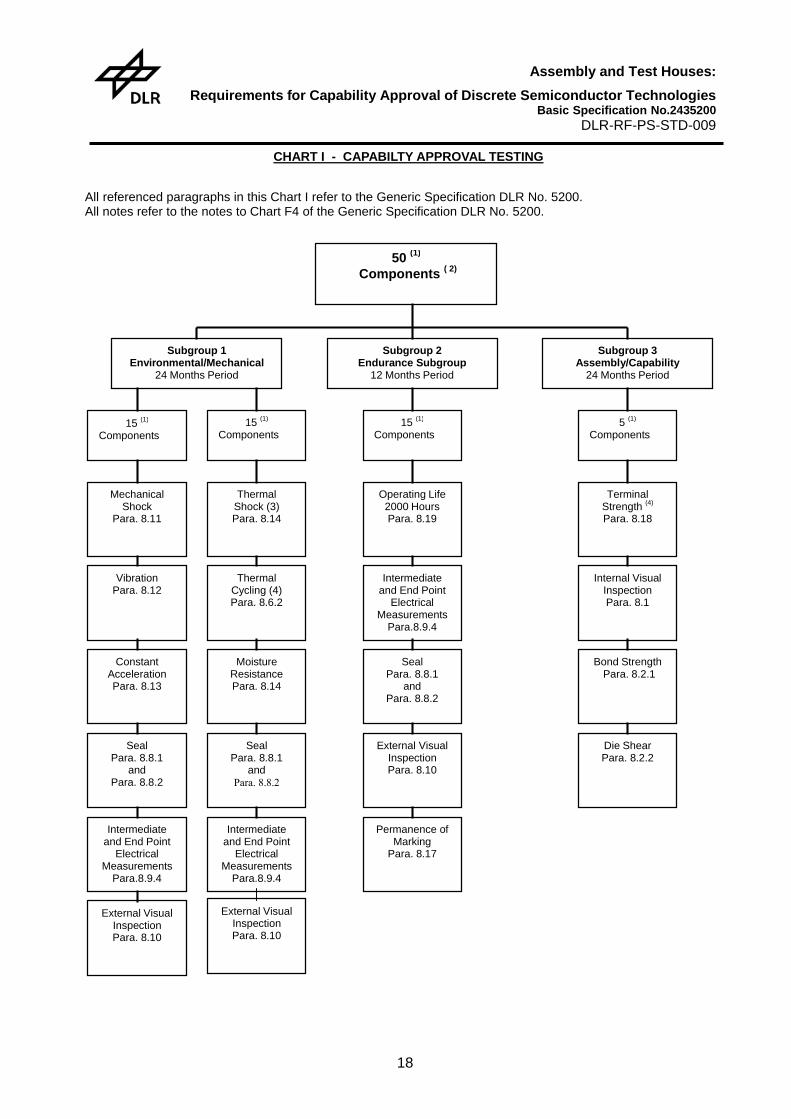
The Capability Approval test programme of these specifications consists of the tests and subgroups given in Chart I of this specification. The test vehicles submitted to Chart I testing shall be the test samples as defined in Paragraph 7 of this specification. All packaging related tests shall be performed on packages which represents the type of packages as stated in the domain description and in the PID.
9.2 CAPABlLITY APPROVAL TEST REPORT
On completion of the Capability Approval testing the manufacturer shall collect all relevant test data and documentation in form of a test report. This report shall be sent to DLR for review and approval.
10. COMPONENT TYPE APPROVAL TEST
For a component type manufactured within a Discrete Semiconductor Capability Domain the qualification procedure of ESCC Basic Specification No.24300 shall apply.
Component type approval testing is only applicable to those components that have been designed and manufactured within the boundaries of an approved Capability Domain and for which a statement of compliance has been issued.
The component type approval testing shall be performed on the specified sample. chosen at random from components which have successfully passed the tests in Charts F2 and F3 of the
Assembly and Test Houses:
Requirements for Capability Approval of Discrete Semiconductor Technologies Basic Specification No.2435200
DLR-RF-PS-STD-009
17
Generic Specification DLR No.5200 and shall consist of an operating life test in accordance with the Generic Specification DLR No.5200, Paragraph 8.19.
Sample size shall be 3 pieces minimum.
Accept criteria shall be zero failures.
11. REDUCTION. EXTENSION AND CHANGE OF THE CAPABlLITY DOMAIN
Any modification such as reduction, extension and change of the Capability Domain shall be in accordance with ESA/SCC Basic Specification No.24300.
In order to classify potential modifications, a matrix shall be included in the domain description for the applicable variant. This matrix shall list the parameters defining the Capability Domain and their interdependence. The importance of a parameter in conjunction with the consequences to related parameters will determine whether a change is minor or major.
For the distinction between minor and major changes the following shall be considered as a general guideline:
Minor changes shall have no or only little impact on the Capability Domain and its boundaries and must be downward compatible (previously designed components must still be manufacturable without redesign or changes to their specification). This may be the case for isolated parameter changes or the replacement of equipment and materials for the purpose of yield enhancement or to improve safety margins.
In case of doubt or if device performance or radiation tolerance is adversely affected changes must be classified as major.
12. PROCUREMENT
Procurement of components manufactured within the capability boundaries shall be in accordance with the requirements of the Generic Specification DLR No.5200 and the applicable Detail Specification.
Assembly and Test Houses:
Requirements for Capability Approval of Discrete Semiconductor Technologies Basic Specification No.2435200
DLR-RF-PS-STD-009
18
CHART I - CAPABILTY APPROVAL TESTING
All referenced paragraphs in this Chart I refer to the Generic Specification DLR No. 5200. All notes refer to the notes to Chart F4 of the Generic Specification DLR No. 5200.
8
50 (1)
Components ( 2)
Subgroup 1 Environmental/Mechanical
24 Months Period
Subgroup 2Endurance Subgroup
12 Months Period
Subgroup 3Assembly/Capability
24 Months Period
15 (1)
Components
15 (1)
Components
15 (1)
Components
5 (1)
Components
Mechanical Shock
Para. 8.11
Vibration Para. 8.12
Seal Para. 8.8.1
and Para. 8.8.2
Constant Acceleration Para. 8.13
External Visual Inspection Para. 8.10
Intermediate and End Point
Electrical Measurements
Para.8.9.4
Intermediate and End Point
Electrical Measurements
Para.8.9.4
Seal Para. 8.8.1
and Para. 8.8.2
Moisture Resistance Para. 8.14
Thermal Cycling (4) Para. 8.6.2
Thermal Shock (3) Para. 8.14
External Visual Inspection Para. 8.10
Seal Para. 8.8.1
and Para. 8.8.2
Intermediate and End Point
Electrical Measurements
Para.8.9.4
Operating Life 2000 Hours Para. 8.19
Permanence of Marking
Para. 8.17
Die Shear Para. 8.2.2
Bond Strength Para. 8.2.1
Internal Visual Inspection Para. 8.1
Terminal Strength (4)
Para. 8.18
External Visual Inspection Para. 8.10