assessment of the semiconductor industry source reduction...
TRANSCRIPT
ASSESSMENT OF THE
SEMICONDUCTOR INDUSTRY
SOURCE REDUCTION PLANNING EFFORTS
The Hazardous Waste Source Reduction and ManagementReview Act of 1989
California Environmental Protection AgencyDepartment of Toxic Substances Control
Office of Pollution Prevention and Technology Development

October 1994
i
REPORT OVERVIEW
The following report summarizes the results of theDepartment of Toxic Substances Control's (Department) assessmentof the semiconductor industry's source reduction review andplanning effort as mandated by the Hazardous Waste SourceReduction and Management Review Act of 1989 (Act). The Actrequired the Department to select at least two categories ofgenerators by SIC (Standard Industrial Classification) Code everytwo years for evaluation. The semiconductor industry wasselected as one of the targeted categories of generators for theyears 1993 and 1994.
To obtain a complete and current picture of source reductionwithin the semiconductor industry since the initial Plans andReports were prepared, the Department sent out a source reductionquestionnaire to 300 semiconductor facilities throughoutCalifornia. The questionnaire consisted of five pages designedto provide the Department with feedback on progress achieved bythe semiconductor industries toward implementing source reductionmeasures since 1991. Generators who were captured by the Act in1990 were requested to complete all five pages of thequestionnaire. A total of 40 completed questionnaires werereturned. The data collected from the questionnaires provide thebasis for the findings presented in this report.
Based on the results of the questionnaires, ten facilitieswere requested to submit their Plans to the Department forfurther evaluation. Facilities were selected based on a numberof factors, including the type of waste streams generated, sourcereduction measures mentioned in the questionnaire, progress inimplementing the source reduction measures, and net reductions inhazardous waste generation as a result of implementing the sourcereduction measures. In addition, facilities that indicated onthe questionnaire that they were captured by the Act but did notcomplete a Plan in 1991 (three facilities), were also requestedto submit a Plan within 30 days upon receipt of the requestletter. The Department is currently working with these threefacilities to assist them in evaluating and implementing sourcereduction measures at their facilities.
Several measurable bases for documenting historical sourcereduction within the semiconductor industry were identified inthe questionnaire. These included wafer starts, production rate,activities, annual sales, and work force size. Thequestionnaires also indicated that data normalization is not

ii
easily achieved in the semiconductor industry. Changes inchemical usage and processes as a result of the rapid advancementof semiconductor fabrication technology create a real challengeto semiconductor industries attempting to normalize their data. In addition, changes in activity level where some fabricationareas ceased operations while others were newly started, alsomade data normalization difficult to achieve.
The questionnaires also indicated that resistance to sourcereduction is primarily due to process sensitivity to mostchanges. Semiconductor production processes are very sensitiveto most changes such as alteration in temperature, gas flow,chemical purity, chemical concentration, and chemical viscosity. In addition, the high initial cost of equipment used forimplementing source reduction measures and lengthy paybackperiods were also mentioned by several semiconductor facilitiesas major deterrents to pursuing specific source reductionmeasures.
Several incentives for reducing hazardous waste generationwithin the semiconductor industry were highlighted in thequestionnaires. Reduction in cost and liability were mentionedextensively as major incentives to source reduction. Otherincentives to source reduction stated in the questionnairesincluded compliance with regulations to create a safer workingplace and a cleaner environment, meeting corporate directives andpolicies, and reducing regulatory and public pressure.
The questionnaire enabled the Department to create acomprehensive list of major wastestreams routinely generated bythe semiconductor industry. The list consisted of:
1) aqueous wastes (containing low concentrations ofhydrofluoric, hydrochloric, and sulfuric acids);
2) solvents; 3) stripper wastes; 4) photoresist waste; and 5) contaminated solid wastes.
Comparing hazardous waste generation between the years 1990 and1993 revealed an increase in some major routinely generatedhazardous waste streams (such as aqueous waste and solidcontaminated hazardous waste) and a decrease in other wastestreams such as solvent wastes, stripper waste, and photoresistwaste. This mixed trend in hazardous waste generation between1990 and 1993 emphasized the fact that a meaningful calculationof the total amount of waste reduction or percentage reductionoccurring within the semiconductor industry could not be obtained

iii
without data normalization. Significant gains in wastereductions achieved as a result of implementing source reductionmeasures were offset by increased production rate and majorchanges in chemical usage as a result of advancement in thesemiconductor fabrication technology.
The Plan review indicated that several semiconductorindustries addressed only hazardous wastewater as the majorhazardous wastestream generated at their facility. SB 1133 wasnot enacted until September 5, 1991 (four days after the initialdue date for the Plans and the Reports). Therefore, generatorswith large quantities of hazardous wastewater had the option toaddress only aqueous waste in their Plans. For the next Plans,due September 1, 1995, generators will be required to determinethe total quantity of wastewater generated, then conductadditional calculations without counting the wastewater toaddress the remaining wastes separately (as mandated by SB 1133). In addition, SB 1726 (enacted in 1992) requires generators toinclude a four-year numerical goal in the next Plans. The goalis a single numerical percentage used to reflect the company'ssource reduction vision over a period of four years.
The questionnaire revealed that several semiconductorfacilities captured by the Act in 1990 have implemented sourcereduction measures initially identified in their 1991 Plans. Thenet reductions achieved as a result of implementing thosemeasures ranged from 1% to 280 % (taking into consideration 300%company growth). Furthermore, all surveyed generators were askedto provide a brief description of one source reduction measureimplemented at their facility. Reduction measures mentioned inthe questionnaires ranged from simple administrative steps suchas improved inventory control and employee training to majorprocess modifications such as installation of a sulfuric acidreprocessor to reduce the amount of aqueous waste sent to thetreatment plant.
Of the 40 returned questionnaires, 20 companies indicatedthat they would like to share the details of the source reductionmeasure mentioned in the questionnaire with the Department. Those companies were requested to provide a one-page descriptionof the measure and to include - whenever feasible - any reductionin hazardous waste generation and any cost savings realized atthe facility as a result of implementing the measure. Severalviable source reduction measures for major hazardous wastestreams were identified based on the information provided bythese companies. Successful approaches to source reduction havebeen included in this report to facilitate technology transfer

iv
among various semiconductor facilities.
v
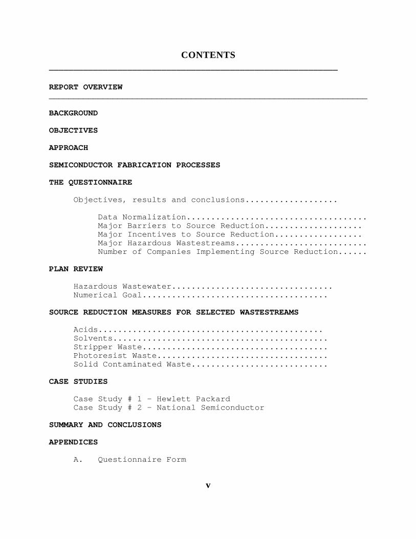
CONTENTS___________________________________________________________
REPORT OVERVIEW_________________________________________________________________
BACKGROUND
OBJECTIVES
APPROACH
SEMICONDUCTOR FABRICATION PROCESSES
THE QUESTIONNAIRE
Objectives, results and conclusions...................
Data Normalization.....................................Major Barriers to Source Reduction....................Major Incentives to Source Reduction..................Major Hazardous Wastestreams...........................Number of Companies Implementing Source Reduction......
PLAN REVIEW
Hazardous Wastewater.................................Numerical Goal......................................
SOURCE REDUCTION MEASURES FOR SELECTED WASTESTREAMS
Acids..............................................Solvents............................................Stripper Waste......................................Photoresist Waste...................................Solid Contaminated Waste............................
CASE STUDIES
Case Study # 1 - Hewlett PackardCase Study # 2 - National Semiconductor
SUMMARY AND CONCLUSIONS
APPENDICES
A. Questionnaire Form

vi
B. Review FormC. Detailed description of source reduction measures
1
BACKGROUND
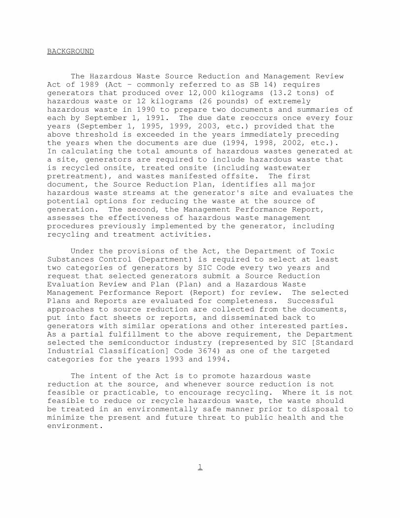
The Hazardous Waste Source Reduction and Management ReviewAct of 1989 (Act - commonly referred to as SB 14) requiresgenerators that produced over 12,000 kilograms (13.2 tons) ofhazardous waste or 12 kilograms (26 pounds) of extremelyhazardous waste in 1990 to prepare two documents and summaries ofeach by September 1, 1991. The due date reoccurs once every fouryears (September 1, 1995, 1999, 2003, etc.) provided that theabove threshold is exceeded in the years immediately precedingthe years when the documents are due (1994, 1998, 2002, etc.). In calculating the total amounts of hazardous wastes generated ata site, generators are required to include hazardous waste thatis recycled onsite, treated onsite (including wastewaterpretreatment), and wastes manifested offsite. The firstdocument, the Source Reduction Plan, identifies all majorhazardous waste streams at the generator's site and evaluates thepotential options for reducing the waste at the source ofgeneration. The second, the Management Performance Report,assesses the effectiveness of hazardous waste managementprocedures previously implemented by the generator, includingrecycling and treatment activities.
Under the provisions of the Act, the Department of ToxicSubstances Control (Department) is required to select at leasttwo categories of generators by SIC Code every two years andrequest that selected generators submit a Source ReductionEvaluation Review and Plan (Plan) and a Hazardous WasteManagement Performance Report (Report) for review. The selectedPlans and Reports are evaluated for completeness. Successfulapproaches to source reduction are collected from the documents,put into fact sheets or reports, and disseminated back togenerators with similar operations and other interested parties.As a partial fulfillment to the above requirement, the Departmentselected the semiconductor industry (represented by SIC [StandardIndustrial Classification] Code 3674) as one of the targetedcategories for the years 1993 and 1994.
The intent of the Act is to promote hazardous wastereduction at the source, and whenever source reduction is notfeasible or practicable, to encourage recycling. Where it is notfeasible to reduce or recycle hazardous waste, the waste shouldbe treated in an environmentally safe manner prior to disposal tominimize the present and future threat to public health and theenvironment.

2
To maintain the above hierarchy, source reduction is definedin the Act as:
1) Any action which causes a net reduction in thegeneration of hazardous waste; or
2) Any action taken before the hazardous waste isgenerated that results in lessening of the propertieswhich causes it to be classified as hazardous.
Furthermore, the Act clearly states that source reductiondoes not include any of the following:
o Actions taken after a hazardous waste is generated.
o Actions that merely concentrate the constituents of thehazardous waste to reduce its volume or that dilute thehazardous waste to reduce its hazardouscharacteristics.
o Actions that merely shift hazardous wastes from oneenvironmental medium to another environmental medium.
o Treatment.
This report focuses on reduction of hazardous wastes withinthe semiconductor industry at the source. Therefore, thediscussed measures herein do not include any recycling ortreatment management practices conducted after the waste has been generated.

3
OBJECTIVES
The increasing cost and liability associated with hazardouswaste management activities have resulted in recognition byregulators and industry alike of the need for source reductionprograms. The Department hopes that this report will assistsemiconductor facilities in evaluating and implementing sourcereduction measures thus creating an atmosphere in which they cangain competitive advantages, while contributing to environmentalimprovement. With this mission in mind, this report is designedto accomplish the following objectives:
o Facilitate technology transfer by presenting viablesource reduction practices currently being applied bymany semiconductor facilities that could bedisseminated to the rest of the industry.
o Determine the number of semiconductor facilitiescaptured by the Act that have complied with therequirements of the Act.
o Determine the number of semiconductor facilities thathave successfully implemented source reduction measurespreviously identified in their Plans.
o Determine the net reduction in hazardous wastegeneration as a result of implementing source reductionmeasures.
o Obtain information on practical methods for measuringsource reduction over time within the semiconductorindustry (i.e., determine the most effective method tonormalize data).
o Highlight major incentives and barriers to sourcereduction within the semiconductor industry.
o Generally, provide industry with practical informationon completing the required source reduction documentsand meeting the requirements of the Act for 1995.
o Provide the Department with an adequate informationbase to determine what needs exist and what actions canbe realistically taken to encourage source reduction.
o Provide feedback to the Department on the effectivenessof its source reduction program.

4
5
APPROACH
The initial approach undertaken by the Department was toreview several Plans and Reports and to use the informationcontained in these documents as the basis to meet the aboveobjectives. Upon further evaluation of this approach, theDepartment realized that the Plans and Reports alone will not besufficient to provide the Department with a complete picture onsource reduction within the semiconductor industry. Specifically, the Plans and Reports were lacking pertinentinformation in the following areas:
o The Act required all generators to identify all majorhazardous waste streams that are routinely generated attheir facilities that have a yearly volume, orcomparable weight, exceeding five percent of the totalyearly volume, or comparable weight of hazardous wastegenerated at the site. A similar calculation wasrequired for extremely hazardous wastes. Generatorswere then required to evaluate source reductionmeasures for these major wastestreams. To achievesignificant reductions in hazardous waste generationwithin the semiconductor industry, it is necessary tofirst obtain comprehensive industry-specific wastegeneration data under the Act. A comprehensive wastegeneration list could not be obtained by reviewing alimited number of Plans.
o In setting the above 5% limits, the Legislatureoverlooked the fact that, at many facilities(especially within the semiconductor industry),hazardous wastewater generation represents the largestpercentage of total waste generated. Therefore, whengenerators apply the above-mentioned 5% rule, only thewastewater will amount to greater than 5% and thusgenerators will address only the wastewater and willnot be required to address other hazardous wastestreams for which SB 14 was originally intended. Thisproblem was later rectified by the enaction of SB 1133which required generators to determine if the totalquantity of wastewater generated exceeds 5%, thenconduct an additional separate calculation excludingthe wastewater to address the remaining hazardouswastes. SB 1133 did not pass until September 5, 1991(five days following the document preparationdeadline). Therefore, a comprehensive source reductionevaluation for all hazardous wastes generated by thesemiconductor industry could not be obtained from theinitial Plans.

6
7
o The Act required captured generators to complete a Planby September 1, 1991 and every four years thereafter,provided that the set threshold in the Act (12,000kilograms of hazardous waste or 12 kilograms ofextremely hazardous waste) is exceeded in the previousyear. The next Plans are due September 1, 1995. Asnoted earlier, the Department is required by the Act toselect at least two categories of generators by SICCode every two years and request that selectedgenerators submit a Plan for review (i.e., for thesecond Plan call-in cycle [1993 and 1994], theDepartment is still required to evaluate Plans whichwere initially written in 1991). The 1991 Plans lackedinformation on the progress achieved by thesemiconductor industries toward implementing the sourcereduction measures mentioned in their initial Plans.
o For the initial SB 14 Reports, facilities were providedwith the option of selecting 1990 as the baseline year. For all subsequent reports, the baseline year will bethe reporting year of the immediately preceding report. For the initial reports completed by September 1, 1991,most facilities elected to use 1990 as the baselineyear. Therefore, the data provided in these reportswere not sufficient to provide the Department with agood feedback on historical source reductionactivities.
Examining the above limitations, it became apparent that theinformation in the Plans and the Reports must be augmented withmore recent data from a wide universe of generators to providethe Department with a current and complete picture on sourcereduction within the semiconductor industry. To meet thisobjective, the Department developed a source reductionquestionnaire (Appendix A). The questionnaire was distributed to300 California semiconductor industries having SIC Code 3674. Inaddition to providing the Department with updated information onhazardous waste generation and source reduction within thesemiconductor industry, the questionnaire was designed to providefeedback to the Department on the following:
o Number of semiconductor companies implementing sourcereduction based on measures previously identified inthe Plans.
o Net reduction in hazardous waste as a result ofimplementing source reduction measures within thesemiconductor industry.
8
o Methods identified by the surveyed semiconductorfacilities regarding practical methods for normalizinghazardous waste generation within the industry.
o Major incentives and barriers to hazardous wastereduction within the semiconductor industry.
o Number of companies captured by the Act that havecomplied with the requirements of the Act.
o Number of semiconductor industries that need assistancein evaluating or implementing source reduction measuresat their facilities, or need guidance in completing thenext Plans/Reports which are due by September 1, 1995.
Based on the results of the questionnaires, ten facilitieswere requested to submit their Plans to the Department forfurther evaluation. Facilities were selected based on a numberof factors, including the type of waste streams generated, sourcereduction measures mentioned in the Plans, progress inimplementing identified source reduction measures, and netreductions in hazardous waste generation as a result ofimplementing the source reduction measures. All facilities wereasked to verify their Plan completeness prior to submittal to theDepartment by using the Completeness Checklist found in AppendixG of the Guidance Manual for the Hazardous Waste Source Reductionand Management Review Act of 1989 - updated May 1994 - (theCompleteness Checklist is included in Appendix B). In addition,facilities that indicated on the questionnaire that they werecaptured by the Act but did not complete a Plan in 1991 (threefacilities), were also requested to submit a Plan within 30 daysupon receipt of the request letter. The Department is currentlyworking with these three facilities to assist them in evaluatingand implementing source reduction measures at their facilities.
The data collected from the Plans and the questionnaireprovide the basis for the findings presented in this report. These include:
1) a discussion of the objectives and contents of thequestionnaire;
2) a summary of the results obtained from thequestionnaire;
3) a summary of the information obtained from the Planscalled-in by the Department (including key issuesidentified from the reviewed Plans to assist generatorsin completing the next Plans by September 1, 1995);
4) a summary of currently applied source reductionmeasures for selected major wastestreams within thesemiconductor industry; and

9
5) two case studies documenting source reduction measuresimplemented by Hewlett Packard and NationalSemiconductor leading to significant reductions inhazardous waste generation and associated costs andliabilities.
In order to understand the source reduction measuresdiscussed in this report, the following section has been includedto present an overview of the processes and waste streamsspecific to the semiconductor industry.
OVERVIEW OF SEMICONDUCTOR FABRICATION PROCESSES
Semiconductors are solid state electrical devices whichperform a variety of functions, including information processingand display, power handling, and conversion between light energyand electrical energy. The finger-nail sized electronic circuitsetched on silicon are critical to the operation of virtually allelectronics from automatic coffee makers and anti-lock brakingsystems to cellular phones and supercomputers.
The production of semiconductor devices starts with theintroduction of elemental silicon, typically called the seed,into sealed quartz ampules at elevated temperatures andpressures. The ampules act as reaction chambers in whichprogressively more silicon is added to the initial seed until acylindrical, crystal mass has formed inside the ampule to aspecified diameter. This final form of the crystal is called aningot. Other materials can be used to form the ingot, such asgermanium, gallium arsenide, gallium phosphate, and galliumarsenic phosphide. Currently, 80% of the ingots manufactured areseeded with silicon. The silicon ingots are then cut withsensitive diamond-tipped saws into circular disks called wafers. The wafers may have diameters between three and nine inches.
The wafers then undergo a photolithographic processinvolving a series of etching, doping, and metallization stepsthat add layers of electronic circuitry onto the wafer inpredtermined patterns. The areas between these patterns on thewafer are "masked" to prevent buildup of circuitry and thusprovide cutting areas to separate the wafers into individualcircuit groupings. The wafer is then cut into these groupings,which are called "microchips." Depending on the application ofthe microchip and the size of the wafer, as many as 100microchips may be produced from one wafer.
A significant feature in producing semiconductor devices isthe use of "clean" rooms that are engineered to minimize dust or

10
other contaminants from landing on the wafers during fabrication. Dust and contaminants can cause malfunctions in the microscopicelectrical circuitry. One can appreciate the need for suchcleanliness since the process requires control of physical andchemical processes on a molecular level to the point where somecircuit lines are only micrometers thick. A speck of dusttrapped in one of these layers of circuitry can ruin an entiremicrochip.

11
This report focuses on the process of creating electricalcircuitry on the silicon wafer. In general, the layers ofcircuitry are interconnected based on specifications for theultimate application of the wafer. Therefore, even though thefabrication processes for the production of wafers can beexplained in general terms, it must be noted that each productionrun and even different sections of the same run may followdifferent process flows and feature different types of equipment. The following is an overall discussion of the major processingsteps and typical hazardous waste generation points of thesemiconductor manufacturing process. The discussed processes maybe applied in various orders and frequencies. The first step insemiconductor fabrication is cleaning of the silicon wafer in anacid bath and then rinsing with deionized water.
Oxidation
Oxidation is the process of forming thin films of silicondioxide, one on top of each other, on the initial surface of thesilicon wafer. The process occurs in quartz ampule reactionchambers in the presence of oxygen or ultra pure water. Wastefrom this step includes silicon dioxide or other raw materialbeing used for wafer fabrication, hydrofluoric acid used to cleanthe quartz chambers, and rinsing water used to clean the wafers.
Photolithography
Photolithography, also known as photomasking or masking, isthe procedure of forming extremely accurate patterns on thewafer's silicon oxide surface. The photomasking process beginswith the semiconductor wafer's oxide coating being covered with athin layer of photoresist containing an organic polymer, byspinning a small quantity on the wafer. The photoresist issensitive to ultraviolet light. When applied to the wafer andexposed to an ultraviolet pattern, the photoresist records theultraviolet pattern without affecting the surrounding area of thewafer. A similar process using light sensitive silver emulsionis used in photography. The wafer is then heated to bond thephotoresist polymer.
Ultraviolet light shinning through a mask containing acircuit pattern determines where the polymer will be exposed. Some photoresist polymers are normally insoluble to a developersolution but become soluble after exposure to ultraviolet light(positive resist) while others behave in a reverse manner(negative resist). The undeveloped photoresist is dissolved andremoved using a stripper containing acids and caustics.
12
The photolithographic process produces much of the wastesgenerated from the semiconductor manufacturing processes. Hexamethyldisilane (HMDS) typically is used as an initial coatingon the wafer's oxide surface to increase the adhesion ofphotoresist. Waste photoresist solvents and developers alsoresult from this process.
For negative photoresist processes, a waste mixture ofisoprene rubber (the photoresist) and the developer (organicsolvents such as xylene and other nonhalogenated hydrocarbons)are produced. Positive photoresist produces a waste stream ofortho-diazo-ketone (the photoresist) and the caustic (thedeveloper).
Etching
Etching is used to dissolve those places on the wafer notcovered by the photoresist. This process exposes the siliconsurface or substrate in preparation for doping with impurities. The etching process primarily uses acids to remove silicondioxide and metals according to the patterns delineated by thephotoresist. Waste sulfuric, hydrofluoric, hydrochloric,phosphoric, nitric, and chromic acids are produced as a result ofetching process. Waste lubricating oils from vacuum pumps usedto evacuate the reaction chambers of the plasma etchers are alsogenerated.
Doping
In doping, diffusion or ion implantation techniquesintroduce impurities into select regions of the wafer substrateto form a boundary between conduction regions. In diffusion, thewafers typically are stacked in a long, heated quartz tube andexposed to gases containing impurities that diffuse into theexposed parts (i.e., areas not masked with photoresist) of thewafer. Ion implanters bombard the wafer with ionized impurities. Junction formation produces solid wastes containing arsenic,antimony, phosphorus, arsine, diborane, and waste vacuum pumpoils.
Metallization
Metallization is the process of depositing complex patternsof conductive material on the wafer to interconnect theintegrated circuits. Metallization wastes differ significantlydepending on the specific plating or coating process used. Thewaste streams from metallization include solutions of preciousmetals, heavy metals, and acids.
13
Included at various stages of the process are rinsing stepsthat utilize electronic grade, distilled, deionized water andthat generate dilute acid/water waste streams. These streamsconstitute the largest volume of hazardous wastewater generatedin the manufacturing process. Typically these streams areneutralized on-site and discharged into a Publicly OwnedTreatment Works (POTW).
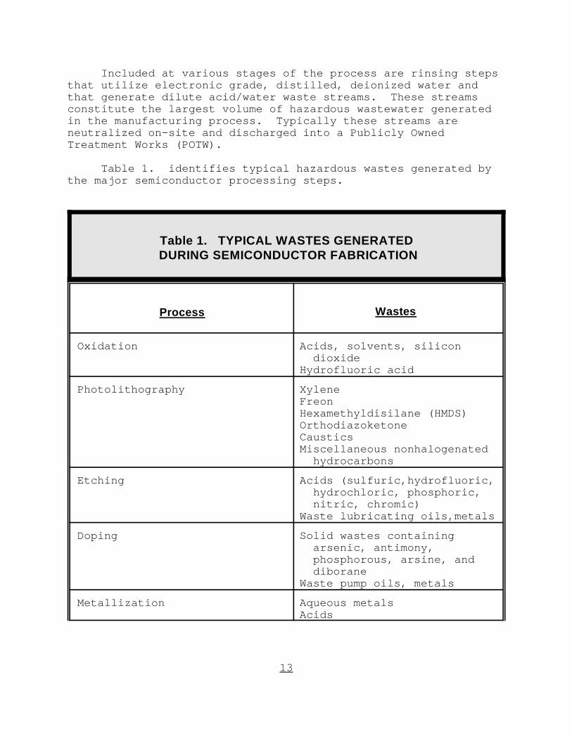
Table 1. identifies typical hazardous wastes generated bythe major semiconductor processing steps.
Table 1. TYPICAL WASTES GENERATED DURING SEMICONDUCTOR FABRICATION
Process Wastes
Oxidation Acids, solvents, silicon dioxide Hydrofluoric acid
Photolithography XyleneFreonHexamethyldisilane (HMDS)OrthodiazoketoneCausticsMiscellaneous nonhalogenated hydrocarbons
Etching Acids (sulfuric,hydrofluoric, hydrochloric, phosphoric, nitric, chromic)Waste lubricating oils,metals
Doping Solid wastes containing arsenic, antimony, phosphorous, arsine, and diborane Waste pump oils, metals
Metallization Aqueous metalsAcids
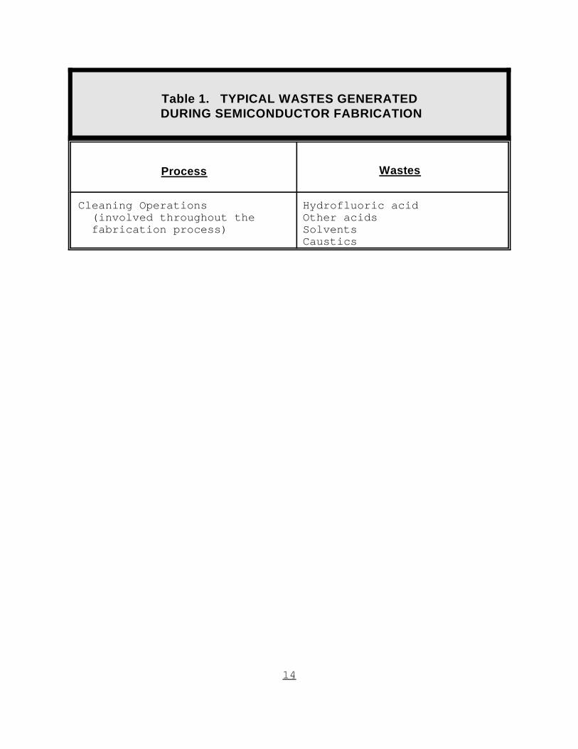
Table 1. TYPICAL WASTES GENERATED DURING SEMICONDUCTOR FABRICATION
Process Wastes
14
Cleaning Operations Hydrofluoric acid (involved throughout the Other acids fabrication process) Solvents
Caustics

15
THE QUESTIONNAIRE - OBJECTIVES, RESULTS AND CONCLUSIONS
The questionnaire consisted of five pages designed toprovide feedback to the Department on the progress achieved bythe semiconductor industry toward implementing source reductionmeasures and documenting net reductions in hazardous wastegeneration as a result of implementing the measures (See Appendix A). The intent of the questionnaire was also toidentify major hazardous wastes generated by the industry, majorincentives and barriers to source reduction within the industry,and practical methods applied by the industry to calculate sourcereduction over time (normalizing hazardous waste generationdata). The questionnaire also served the double purpose ofcollecting source reduction measures from the industry andlocating facilities within the industry that need assistance inidentifying source reduction measures at their facilities. Finally, the questionnaire was designed to provide feedback tothe Department on the effectiveness of its source reductionprogram and to identify key issues which should be emphasized tothe industry in the Department's outreach effort for the nextreporting cycle that concludes September 1, 1995.
The questionnaire was mailed to 300 semiconductor industrieswithin California having SIC Code 3674. This included severalnon-manufacturing industries which either did not generate anyhazardous wastes or generated small quantities of hazardous wasteand were therefore not captured by the Act. The first twoquestions were designed to eliminate companies which did notgenerate hazardous wastes or were not captured by the Act. Thesecompanies were requested to mark questions #1 and/or #2 with "No"and to return the questionnaire to the Department to avoidfurther requests from the Department. A total of 120questionnaires were returned marked "No" on the first and/orsecond questions. The Department randomly chose twenty returnedquestionnaires and verified the information by checking theHazardous Waste Management Information System (HWIS). The dataverification indicated that none of the twenty facilities hadmanifested over 12,000 kilograms of hazardous waste offsite andit was thus concluded that the information submitted in therandomly chosen questionnaires was valid.
Generators who marked both questions #1 & #2 with "Yes" wererequired to complete the remainder of the questionnaire. Question #3 was designed to provide feedback to the Department onthe number of companies captured by the Act that have compliedwith the requirements of the Act and have completed thePlan/Report by the September 1991 due date. Of the 40 returnedcompleted questionnaires, three companies indicated that theywere captured by the Act but did not complete a Plan/Report in

16
1991. All three companies were sent letters requesting them tosubmit a Plan to the Department within 30 days upon receipt ofthe letter. The Department is currently working with these threecompanies to assist them in evaluating and implementing sourcereduction measures at their facilities. The facilities were alsoprovided with guidance materials to assist them in meeting therequirements of the Act.
Questions #4 and #5 were intended to provide feedback to theDepartment on major incentives and barriers experienced by theindustry when implementing source reduction. Under question #6generators were asked to state the best method to be used attheir facilities for data normalization; generators were alsorequested to indicate whether they have actually normalized thedata at their facilities (question #7).
All surveyed generators were asked to provide a briefdescription of one major source reduction measure implemented attheir facilities (question #8). To obtain more detailedinformation on the source reduction measure, generators wereasked whether they were interested in sharing information ontheir source reduction accomplishments with the Department(question #9). Of the 40 returned questionnaires, 20 companiesindicated that they would like to share detailed information onthe source reduction measure mentioned under question #8 with theDepartment. Those companies were requested, in writing, toprovide a one-page description of the source reduction measureand to include information - whenever feasible - on hazardouswaste reduction and any cost savings realized by the facilitiesas a result of implementing the source reduction measure.
To disseminate information collected from the questionnairesto other semiconductor industries, the Department requestedgenerators to indicate under question #10 whether they areinterested in obtaining additional information from theDepartment on source reduction measures within the semiconductorindustry. Of the 40 returned questionnaires, 34 companies marked"Yes" on this question. One company stated that they will beclosing down operations at their facility and are therefore notinterested in obtaining information from the Department.
In addition, all surveyed generators captured by the Actwere asked to complete three tables, Table IA, IB, and Table II. In Table IA, generators were asked to identify major routinelygenerated hazardous waste streams produced at their facilitiesduring the initial reporting year (1990). Similarly, in TableIB, generators were asked to identify major routinely generatedhazardous wastes generated at their facilities during 1993. Byevaluating and comparing the information submitted in both

17
tables, the Department was able to create a comprehensiveindustry-specific waste generation list and to identify trends inhazardous waste generation within the semiconductor industry overthe three years since the baseline year 1990.
18
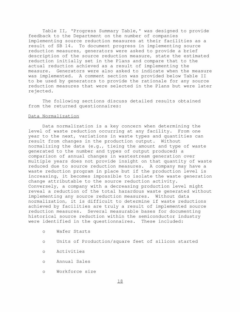
Table II, "Progress Summary Table," was designed to providefeedback to the Department on the number of companiesimplementing source reduction measures at their facilities as aresult of SB 14. To document progress in implementing sourcereduction measures, generators were asked to provide a briefdescription of the source reduction measure, state the estimatedreduction initially set in the Plans and compare that to theactual reduction achieved as a result of implementing themeasure. Generators were also asked to indicate when the measurewas implemented. A comment section was provided below Table IIto be used by generators to provide the rationale for any sourcereduction measures that were selected in the Plans but were laterrejected.
The following sections discuss detailed results obtainedfrom the returned questionnaires:
Data Normalization
Data normalization is a key concern when determining thelevel of waste reduction occurring at any facility. From oneyear to the next, variations in waste types and quantities canresult from changes in the production output. Withoutnormalizing the data (e.g., tieing the amount and type of wastegenerated to the number and types of output produced) acomparison of annual changes in wastestream generation overmultiple years does not provide insight on that quantity of wastereduced due to source reduction measures. A company may have awaste reduction program in place but if the production level isincreasing, it becomes impossible to isolate the waste generationchange attributable to the source reduction activity. Conversely, a company with a decreasing production level mightreveal a reduction of the total hazardous waste generated withoutimplementing any source reduction measures. Without datanormalization, it is difficult to determine if waste reductionsachieved by facilities are truly a result of implemented sourcereduction measures. Several measurable bases for documentinghistorical source reduction within the semiconductor industrywere identified in the questionnaires. These included:
o Wafer Starts
o Units of Production/square feet of silicon started
o Activities
o Annual Sales
o Workforce size

19
20
Wafer starts is defined as the number of times a waferundergoes the series of processing steps described herein under"Overview of Semiconductor Fabrication Processes". Wafer startsis a meaningful measure of waste reduction because it is directlycorrelated to chemical usage and is accurately measured by thesemiconductor manufacturers.
Units of production translates as the number of siliconwafers or the square feet of silica processed on an annual basis. Making the assumption that the wafer size and the "wafer starts"remain constant, units of production can be proven to be aneffective method for measuring source reduction over a period oftime.
Activities is defined as any specific step required duringthe manufacturing process. In semiconductor manufacturing, acombination of up to 200 activities might be required to processa wafer. Furthermore, advanced chips require more processing perwafer thus adding to the number of activities and the complexityof the process conducted to obtain a final product. Examples ofactivities provided in the questionnaire included the precleaningprocess step, inspection, measurement, etching, and spin drying. By tracking activities, the semiconductor industry can determinethe true chemical usage per production level. This measure mighttherefore prove to be more accurate than using production levelor wafer starts.
Measuring waste reduction in terms of annual salesintroduces variables that are not directly correlated to chemicalusage, such as fluctuating market prices and decreases inindustrial activity. Sufficient data are not available to drawany conclusions relating long-term sales figures to productionactivity. Only one facility stated sales as a meaningful measureof normalizing data.
The last option, measuring waste reduction in terms of thenumber of employees, would also introduce variables which are notdirectly related to chemical usage. One semiconductor researchfacility normalized the data based on employment figures. For aresearch facility this approach might be appropriate where anincrease in the number of employees might indicate that moretesting is being conducted at the research lab and consequentlymore hazardous waste is being generated. This approach, however,might prove impractical for a manufacturing facility with highlevels of activity variation.
Whereas most semiconductor facilities managed to normalizedata at their facilities with no major difficulties, fewcompanies were faced with a real challenge when attempting tonormalize their data. Changes in chemical usage as a result of

21
advancement of the semiconductor fabrication process made datanormalization more difficult to achieve. For example, theincreased layers of photoresist applied to the wafer and theaddition of the edge bead removal step to the fabrication process- both introduced to improve product quality - have resulted inan increase in the volume of waste solvent generated. Inaddition, changes in activity level where some fabrication areasceased operation while other areas were newly started, also madedata normalization more difficult. The introduction of a newfabrication line can result in an increase in hazardous wastegeneration. The start-up activities involve the introduction ofmany pieces of new equipment. Extensive flushing of all newequipment with specific chemicals prior to production start-up isnecessary, to bring them into compliance with tight operationalpurity requirements. Therefore, until a new fabrication line isoperating at full capacity, a clear indication of hazardous wastereduction could not be easily achieved.
Major Barriers to Source Reduction
The very nature of the semiconductor industry, with itsemphasis on product quality, ever changing product design, andthe need to survive in a competitive marketplace all combine toconstrain the implementation of waste reduction programs. Inorder to stay competitive in a highly market-driven industry, asemiconductor company must continually improve its productquality to satisfy consumer demands. As fabrication processesare modified in response to these market demands, productionmanagers must focus on using only those materials that ensureproduct specifications are met.
The questionnaires indicated that resistance to sourcereduction is primarily due to process sensitivity to mostchanges. The semiconductor industry is very sensitive to mostprocess changes such as change in temperature, gas flow, chemicalpurity, chemical concentration, and chemical viscosity. Anexample of change is to reduce chemical usage and waste generatedby extending acid bath life, but as the life of the acid isextended the residual byproduct concentration and particle countincreases which potentially increases the defect rate and affectthe ultimate product yield. This is a classic problem in theindustry.
To minimize risks, process changes require qualificationtests. These tests may take up to six months before a processchange is approved and implemented. In addition to creating aproblem with meeting stringent production schedules, incorrectchanges have had serious implications on product quality andyield. One company emphasized that their product is used forhuman heart pace-makers where a defect in the product can have

22
major consequences. This was the main reason for theconservatism to change and the resistance of process managers toimplement changes.
Often in the semiconductor industry, the process engineersare trying to control physical and chemical processes at themolecular level. Many of the physical and chemical factorsaffecting a manufacturing step are not always understood. Therefore, process steps, including specific chemical usage andoperating procedures, are often dictated by the experiences ofthe fabrication managers, who may be reluctant to change thesteps by substituting chemicals, reducing chemical usage, orchanging operating procedures. For example, spinners used todeposit photoresist on the wafers are generally run at 3000 to6000 rpm. This speed is set based on past experience, andalthough the wafers have become thinner and lighter as a resultof technological improvements, this speed has remained the same.
Some of the existing federal and state regulations cansometimes discourage companies from pursuing a certain sourcereduction measure. For example, major process modificationsimplemented to reduce hazardous waste generation may require anauthorization from the Department. Furthermore, under RCRA, onsite treatment of a hazardous waste requires a Part A and Part B permit to operate a treatment, storage, and disposalfacility (TSDF), unless an exemption applies. Obtaining a TSDFpermit involves extensive application requirements and regulatoryapprovals. This process may discourage some facilities considering process modifications to implement source reductionmeasures which could be considered "treatment" under RCRA.
In addition to the permit restrictions associated with RCRA,several companies, with wastewaters managed under NationalPollutant Discharge Elimination System (NPDES) permits, that havewanted to increase or modify their operations have been reluctantto do so. Expansion or modification to their onsite operationscould require revision to their existing NPDES permit toauthorize a change in the composition and flow rate of theirdischarge. The process of revising a NPDES permit and thepotential for more stringent discharge limitations hasdiscouraged companies from modifying or expanding theiroperations.
Several companies stated cost of new equipment purchased toaid in implementing source reduction measures as a major barrierto source reduction. In general, high initial costs coupled withlengthy payback periods would render a source reduction measureeconomically infeasible. One company stated that their Research& Development branch is in Japan, which makes operational andequipment changes even more complicated.

23
Major incentives to Source Reduction
Several incentives for reducing hazardous waste generationwithin the semiconductor industry were highlighted in thequestionnaire. Reduction in cost and liability were mentionedextensively as the major incentives to source reduction. Regulations which required the upgrading of RCRA-approvedlandfills have resulted in a dramatic increase in landfillingcosts. Coupled with the rising cost of landfilling is the landdisposal restriction program enacted under the 1984 amendments toRCRA involving a staged approach to ban the disposal of certainhazardous wastes over a period of years.
As a direct result of the landfill bans, the rising cost oflandfilling, and the ever increasing shortage of available fullypermitted landfill capacity, industry has been forced to turn toalternate waste management practices. As stated earlier, sourcereduction is considered the most efficient and appropriateapproach within the waste management hierarchy.
Indirect costs for waste management can also occur throughthe offsite disposal of wastes involving the risks associatedwith:
1) Transportation of the waste;
2) The potential for mismanagement of the waste by thefacility operators; and
3) The possibility of improper design or operation of the
disposal facility resulting in a release ofcontaminated material into the environment.
Since generators are financially responsible for propermanagement of the waste from the "cradle to grave", generatorscan be held financially responsible for the entire remediation orrestoration of a facility to which they have shipped waste. Therefore, reduction in liability was considered one of the majorincentives for source reduction by the surveyed semiconductorindustries.
Other incentives to source reduction mentioned in thequestionnaire included:
o Compliance with regulations to create a safer workingplace and a cleaner environment.
o Meeting corporate directives and policies.

24
o Reducing regulatory and public pressure.
Major Hazardous Wastestreams
A review of the total quantities of hazardous wastesgenerated in 1990 by the semiconductor industries revealed thatthe aqueous waste stream (containing low concentrations ofhydrofluoric acid, hydrochloric and sulfuric acid) represents thelargest volume of major hazardous waste routinely generated bythe semiconductor industry. Solvent wastes represent the secondlargest waste stream generated by the industry. Other majorroutinely generated hazardous wastestreams reported in thequestionnaire included:
1) stripper waste; 2) photoresist waste; and 3) solid contaminated waste.
Waste oil and calcium fluoride wastes also appeared lessfrequently in Table IA as major routinely generated hazardouswastes.
Comparing hazardous waste generation between 1990 and 1993(Table IA and Table IB) revealed approximately a 50% increase inaqueous wastes (386 million gallons were reported in 1993 ascompared to 199 million gallons in 1990). A slight increase(approximately 10%) was noticed in the quantity of solidcontaminated hazardous waste generated. Conversely, a decrease(approximately 30%) in the quantity of solvent and stripper wastewas reported. Furthermore, a 50% decrease was noticed in thequantity of photoresist waste generated.
The above figures emphasize the fact that a meaningfulcalculation of the total amount of waste reduction or percentagereduction occurring within the semiconductor industry could notbe obtained without data normalization. Between the years 1990and 1993 variations in waste quantities stemming from changes inchemical usage coupled with increased production rate, distortedthe waste reduction figures obtained as a result of implementingsource reduction measures. For example, significant gains madeby implementing source reduction measures to reduce the quantityof solvent waste were offset by the introduction of the edge beadremoval step which resulted in an increase in solvent usage. Similarly, a slight increase in the total quantity of solidcontaminated hazardous wastes was realized in spite of theintroduction of several source reduction measures to specificallyaddress this waste stream. In general, the increase in wastegeneration - especially aqueous waste - could be attributedmainly to increased production between the years 1990 and 1993.

25
On the other hand, the 50% decrease in the quantity ofphotoresist generated could have resulted from chemicalsubstitution used widely by the semiconductor industries toswitch from negative to positive photoresist between the years1990 and 1993.
Number of Companies Implementing Source Reduction
The questionnaires revealed that several semiconductorindustries captured by the Act in 1990 have implemented sourcereduction measures initially identified in their 1991 Plans. This conclusion was reached based on the information presented inTable II, "Progress Summary Table," which was designed to providefeedback to the Department on the number of companiesimplementing source reduction measures at their facilities as aresult of SB 14. Of the 40 returned questionnaires, 37 companiesindicated at least one source reduction measure which wasimplemented based on the Plan. Table 2 highlights some of themajor source reduction measures implemented by the facilities.
Table II also revealed that the net reductions in hazardouswaste generation achieved as a result of implementing the sourcereduction measures ranged from 1% to 280 % (taking intoconsideration 300% company growth). Therefore, based on theresults obtained from the 40 completed questionnaires it can beconcluded that the Act has motivated implementation of sourcereduction measures and has contributed to a net reduction inhazardous waste generation in California. Several facilitiesalso highlighted in Table II source reduction measures which wereimplemented prior to the enaction of SB 14. These measures aresummarized in Table 3.
Several companies provided the Department with detailedinformation on the source reduction measures mentioned in thequestionnaires. These measures are highlighted by an asterisk inTables 2 & 3 - detailed information on each measure is includedin Appendix C. Source reduction measures mentioned in thequestionnaires ranged from simple administrative steps such asimproved inventory control and employee training to major processmodifications such as installation of a sulfuric acid reprocessorto reduce the amount of aqueous waste sent to the treatmentplant.
A comment section was provided below Table II to be used bygenerators to provide the rationale for any source reductionmeasures that were selected in the Plans but were later rejected.The completed questionnaires indicated that the main reason forrejecting measures previously selected in the Plans was thechange in activity level where some fabrication areas were closed

26
down while others were newly started thus making it difficult toimplement certain source reduction measures initially designedfor the old fabrication area.

Detailed description of source reduction measure is included in Appendix C.1
27
Table 2. COMPANIES IMPLEMENTING SOURCE REDUCTION
MEASURES BASED ON SB 14 PLANS
Company Hazardous Process Source Percentag DateWaste Generated Reduction e Implemente
Streams Waste Measure Reduction d
IC Sensors Waste Etching Changed 1.1 HF 280% 6/93hydrofluoric bath less "normal-acid frequently izedsolution company
growth300%
Loral HF Etching Operational 100% duringFairchild Wastewater Improvement, 1993Imaging Installed monitor
and alarm systems,modifiedequipment. 1
Samsung Wastewater Etching Chemical 88% 10/92substitution: NaC10 for HCL
Samsung Wastewater Etching Process 99% 10/92modification andchemicalsustitutions: NaC10 for H S02 4

Table 2. COMPANIES IMPLEMENTING SOURCE REDUCTION
MEASURES BASED ON SB 14 PLANS
Company Hazardous Process Source Percentag DateWaste Generated Reduction e Implemente
Streams Waste Measure Reduction d
The actual source reduction method reduced the quantity of acid stream influent to2
the process waters rather than reducing the volume of process waters.
28
Silicon HF acid Wafer Extend bath life 20% 1992Systems cleaning
LSI Logic HF acid Cleaning Extend useful bath 100% 8/92solutions life1
Advanced Process Photolitho- Increasing bath HCL 25% 4thMicro Devices waters with graphy residence time. quarter of
low pH cleaning 1992
1
Advanced Process Cleaning Input changes and NH OH 34% 4thMicro Devices waters with process HCL 26% quarter of
low pH modifications for H 0 29% 1992wafer cleaning.1
4
2 22
Integrated Water with Cleaning Eliminated rinse 100% 5/94Device organics water by carbonTechnology adsorption.
Silicon HF Cleaning Recycle/reprocess 8.3% 4thSystems Wastewater sulfuric acid used quarter of
in clean sinks 1991

Table 2. COMPANIES IMPLEMENTING SOURCE REDUCTION
MEASURES BASED ON SB 14 PLANS
Company Hazardous Process Source Percentag DateWaste Generated Reduction e Implemente
Streams Waste Measure Reduction d
29
IC Sensors Waste Cleaning Improved security 56% 2/92flammable on storage areas,liquids employee training
Linear Waste Wafer clean Process change in 40% 3/94Technology flammable the backlappingCorporation liquids operation to
eliminate solventusage
International Halogenated Backlapping Solvent based 100% 10/92Rechfix solvents protective
coatings werereplaced with awater removablepolymeric "tape".
Silicon Acetone Phototitho- Switched to an 100% 1993Systems graphy edge alternative
bead removal chemical(Microposit-10) inplace of acetone.
SGS Thomson Non- Photolitho- Purchasing and 246 1/1992Microelec- halogenated graphy inventorytronics solvents Cleaning management

Table 2. COMPANIES IMPLEMENTING SOURCE REDUCTION
MEASURES BASED ON SB 14 PLANS
Company Hazardous Process Source Percentag DateWaste Generated Reduction e Implemente
Streams Waste Measure Reduction d
30
Rohm Bulk Cleaning and Minimal dispensing 20% duringCorporation Solvents Photolitho- of developer and 1992(Kifer Road) graphy IPA
EG&G Reticon Waste Cleaning and Chemical 81% 9/93Stripper Photolitho- substitution with
graphy alternatives.1
Integrated Photoresist Photolitho- Calibrated 15% duringDevice graphy photoresist 1992Technology dispenser to
reduce amount ofphotoresistdispensed to 4 ml.per dispenseinstead of 5 to6 ml.
Integrated Flammable Cleaning Improved policies 100% 5/94Device wipes and procedures -Technology better operating
practices.1
EG&G Reticon Solid Cleaning Employee Training 97% 1/7/93contaminatedwastepacks/spilldebris

Table 2. COMPANIES IMPLEMENTING SOURCE REDUCTION
MEASURES BASED ON SB 14 PLANS
Company Hazardous Process Source Percentag DateWaste Generated Reduction e Implemente
Streams Waste Measure Reduction d
31
SGS Thomson Waste oil Equipment Installation of 85% 1/1992Microelec- Maintenance dry pumpstronics
Detailed description of source reduction measure is included in Appendix C.1
32
Table 3. COMPANIES IMPLEMENTING SOURCE REDUCTION
PRIOR TO SB 14 PLANS
Company Hazardous Process Source Percentag DateWaste Generated Reduction e Implemente
Streams Waste Measure Reduction d
Rohm Wastewater Cleaning Changed processes 42% 8/1990Corporation and modified
equipment1
Ardrox Wastewater Cleaning Shut off constant 55% 5/91flow DI water.
Raytheon Waste Cleaning Inventory Control 48% duringsolvent 1991
Intel Unspecified Wafer Change wafer 57% duringsolvent cleaning cleaning less 1991mixture often.1
Sen Sym Flammable Wafer More efficient 18% 1/91liquids cleaning cleaning
Rohm Hazardous Etching and Containers washed 93% 6/91Corporation waste solid Phototitho- in machine to
graphy become clean
Advanced Debris and Etching, Bulk chemical 29% 4thMicro rags phototitho- distribution quarter ofDevices graphy and 1991
cleaning
33
PLAN REVIEW
After reviewing the completed questionnaires, ten facilitieswere asked to submit the entire Plan for further evaluation andin-depth review. The choice of which facilities were to beselected for a detailed review was made based on a number offactors, including the type of waste streams generated, sourcereduction measures mentioned in the Plans, progress inimplementing the source reduction measures, and net reductions inhazardous waste generation as a result of implementing sourcereduction measures. Facilities that provided impressive sourcereduction information (e.g., innovative measures, significantreductions, etc.) were requested to send in the entire Plan. Allfacilities were asked to verify their Plan completeness prior tosubmittal to the Department by using the Completeness Checklistfound in Appendix G of the Guidance Manual for the HazardousWaste Source Reduction and Management Review Act of 1989. Successful approaches to source reduction were collected from thePlans and are included herein under "Source Reduction Measuresfor Selected Waste Streams." In addition, three facilities thatindicated on the questionnaire that they were captured by the Actbut did not complete a Plan in 1991, were also requested tosubmit Plans. The facilities were granted 30 days to completethe Plan. The Department is currently working with these threefacilities to assist them in completing the Plans by the settimeline.
Hazardous Wastewater
SB 14 required generators to identify and perform a sourcereduction review and plan for "all routinely generated hazardouswaste streams which result from ongoing processes or operationsand that have a yearly volume exceeding five percent of the totalyearly volume of hazardous waste generated at the site, or, forextremely hazardous waste, five percent of the total yearlyvolume of extremely hazardous waste generated at the site." Insetting the above limits, the Legislature overlooked the factthat, at many facilities, hazardous wastewater generationrepresents the largest percentage of total waste generated. Therefore, when generators apply the above-mentioned five percentrule, only the wastewater will amount to greater than fivepercent and thus generators are required to address only thewastewater and will not be required to address other hazardouswaste streams for which SB 14 was originally intended.
This problem was later rectified by the enaction of SB 1133which required generators to determine if the total quantity ofwastewater generated exceeds five percent, then conductadditional calculation excluding the wastewater to address the

34
remaining hazardous wastes separately.

35
SB 1133 did not pass until September 5, 1991. As theinitial SB 14 Plans/Reports were due on September 1, 1991,generators with large quantities of hazardous wastewaters had theoption to address only the wastewater. Approximately 40% of thePlans reviewed addressed hazardous wastewater as the only majorwastestream thus overlooking any other hazardous wastes generatedat the facilities. Companies that addressed only the hazardouswastewater were sent letters informing them of the need toaddress all the major hazardous wastes generated at the facilityas mandated by SB 1133 for the next Plans due to be completed bySeptember 1, 1995. The Department also referred those generatorsto page 19 of the updated Guidance Manual, which includes adetailed description on how the aqueous waste stream should beaddressed.
Numerical Goal
In 1992, the Legislature enacted SB 1726 modifying therequirements of SB 14 and creating a new universe of generatorswho are captured by the Act. The Department has updated itsGuidance Manual to reflect the changes in the Act. One of themajor modifications to the Plan format as a result of enaction ofSB 1726 is the requirement for the inclusion of a four-yearnumerical goal in the next Plans. The numerical goal is anestimate of the source reduction that a company could optimallystrive to achieve over the next four years. For example, for thePlans due to be completed by September 1, 1995, the numericalgoal covers the four years from the end of the current reportingyear (January 1, 1995) through the end of the next reporting year(December 31, 1998). The goal is a single numerical percentageused to reflect the company's source reduction vision over aperiod of four years. The goal must reflect waste streamreductions due to source reduction and must exclude any effectsdue to production or economic influences. Detailed informationon how to calculate the four-year numerical goal is included onpage 32 of the updated Guidance Manual.

36
SOURCE REDUCTION MEASURES FOR SELECTED WASTE STREAMS
A number of viable source reduction measures within thesemiconductor industry were identified based on thequestionnaires and the reviewed Plans. The following sectiondescribes waste reduction methods applied by severalsemiconductor firms addressing the following major wastestreams:
1) Aqueous wastes (containing low concentrations ofhydrofluoric, hydrochloric, and sulfuric acids);
2) Solvents; 3) Stripper wastes; 4) Photoresist waste; and 5) Contaminated solid wastes.
Aqueous wastes
Hazardous wastewater is the largest waste stream generatedby the semiconductor industry. The manufacturing of deionized(DI) water uses large amounts of acids (mainly sulfuric andhydrochloric acids) by the semiconductor companies. Waterconservation practices within the industry have led to asubstantial decrease in the use of sulfuric and hydrochloricacids since less water generated means using less chemicals. Reduction in water consumption has been achieved by switchingfrom continuous flow to on-demand rinsing in the fabricationoperations, redesigning the water reclamation system, improvedmaintenance methods for leaks and the use of reclaimed water inscrubbers and cooling towers.
The effect of the above reduction measure has been enhancedby another source reduction measure implemented in the DI watergeneration area. Deionized water is produced by first treatingmunicipal supply water, typically groundwater, with a reverseosmosis process prior to the ion exchange final treatment. Thereverse osmosis removes much of the water impurities, thusgreatly extending the recharge period of the ion exchange beds. Substitution of thin film composite (TFC) membranes withcellulose acetate (CA) membranes in the reverse osmosis processhas resulted in obtaining better water quality and at the sametime reducing the sulfuric acid used to adjust the pH of thereverse osmosis feedwater. Since acid is also used in theregeneration of the resin, the membrane substitution has improvednot only the quality of the generated water and reduced the acidused for the pH adjustment, but it has also doubled the run timeof the resin thus reducing the acid used to regenerate the ionexchange beds.
Reducing acid bath waste by extending the bath replacementperiod is another alternative evaluated by the semiconductor

37
industry. Wafers are rinsed in acid baths several times duringthe cleaning and etching processes. The baths are usuallydisposed of and replaced on a set time schedule regardless ofusage. Many semiconductor industries have modified the criteriafor acid bath replacement. Baths are now often being replacedafter a specific number of wafers have been processed or afterphysical/chemical changes in bath composition have been observedrather than after a set time period. In addition wafers arerinsed consecutively in several baths during many rinsingprocesses. Many semiconductor facilities studied bath rotationsand implemented programs to train employees on the newspecifications for bath rotations to reduce the chances of crosscontamination and subsequently reduce the quantity of acid wastegenerated.
Sulfuric acid
A net reduction in the overall discharge of sulfuric acidhas been realized by using an acid reprocessor to purify thespent sulfuric acid used in the sulfuric clean sinks and thesulfuric strip sinks. Because the sulfuric acid would berecycled and reused, there would be a significant reduction inthe quantity of hazardous chemicals purchased and the quantity ofsulfuric acid discharged to the wastewater treatment facilitywould be reduced.
The neutralization products of sulfuric acid and sodiumhydroxide are sodium sulfate and water. Neither of theseproducts are classified as hazardous. Therefore, assumingcomplete neutralization, the effluent from the wastewatertreatment facility which is being discharged to water contains nohazardous waste.
In manufacturing integrated circuits, silicon wafers areprocessed through a series of process steps which build layers ofmaterial onto the silicon substrate. These layers willultimately form the devices (circuits) which will conductelectricity and perform the described functions.
It is extremely critical that the wafers be cleaned beforeeach process step to avoid contamination as unwanted impurities,films, and particulate matter will have a devastating effect onelectrical characteristics of the manufactured devices.
Wafer cleaning is accomplished using a mixture ofconcentrated sulfuric acid and hydrogen peroxide. The mixing ofthese two chemicals produces an exothermic reaction which heatsthe mixture and accelerates the cleaning process. As the bath

38
temperature rises, the hydrogen peroxide decomposes to form waterand oxygen. This produced water dilutes the mixture resulting inthe need to add more hydrogen peroxide to maintain the desiredcleaning rate and mixture temperature. A mixture is consideredspent, ready for discharge to the wastewater treatment facility,when either the addition of hydrogen peroxide can no longerachieve and maintain the desired bath temperature or the numberof particles present in the bath exceeds process specificationrequirements.
This cleaning mixture is used in clean sinks and stripsinks. In the clean sink, as the name implies, the wafers arecleaned before critical process steps are performed. In thestrip sinks, the mixture is used to remove photoresist which wasused to mask certain portions of the wafer in the preceding etchstep.
As an alternative to discharging the spent mixture ofsulfuric acid and hydrogen peroxide to the wastewater treatmentfacility for disposal treatment, a sulfuric acid reprocessor canbe used to reclaim the mixture for reuse in the sinks. AlamedaInstruments, Inc. and Athens Corporation are manufacturers ofthis type of equipment. Both manufacturing companies useautomated computer controlled vacuum distillation to purify andconcentrate the sulfuric acid. As part of the computer control,an on-line monitoring system analyzes and compares the producedsulfuric acid concentration and particulate concentration to userprogrammable process specifications requirements. Any detectedoff-specification product is returned to the vacuum distillationchamber for reprocessing. As sulfuric acid is purified,peroxydisulfuric acid (PDSA) can be produced in situ orphysically added to replace hydrogen peroxide. Integratedcircuit manufacturer's have found PDSA to be an acceptablereplacement for hydrogen peroxide use in both the sulfuric acidclean and strip sinks.
Because PDSA produces a smaller quantity of water upondecomposition when mixed with sulfuric acid compared to hydrogenperoxide, the substitution of PDSA for hydrogen peroxideessentially eliminates bath dilution effects. On a volume-to-volume basis, less PDSA is required to obtain the same cleaningcharacteristics achieved by using hydrogen peroxide.
Along with eliminating the need for hydrogen peroxide, lowergrade sulfuric acid and PDSA can be purchased and purified to thedesired specifications in the acid reprocessor which would resultin a raw chemical cost savings. Once the system is in operation,the monthly sulfuric acid consumption by the sulfuric acid sinkscan be reduced by as much as 90%. The remaining ten percent is

39
the sum of mixture evaporation, wafer carry over, and a wastestream used to remove particulate matter buildup from thereprocessor.
Another major source reduction measure for reducing theoverall use of sulfuric acid is the replacement of the standarddiffusion sulfuric sinks with filtered, recirculating units. Tritec and Bold are two manufacturers of this type ofrecirculating sinks. Recirculation and filtration allowconsiderable extension of the acid bath service life. Byrecirculating and filtering, the quantity of sulfuric aciddischarged to the wastewater treatment facility will besignificantly reduced.
In general, unfiltered sulfuric sinks in the diffusion areaof the fabrication area use three parts sulfuric acid to twoparts hydrogen peroxide. As noted previously, the exothermicreaction which takes place between these two chemicals heats thebath and accelerates the cleaning process. The bath mixture mustbe changed frequently because it becomes diluted as the hydrogenperoxide decomposes to water.
The life of the acid could be greatly extended by usingsinks which are able to heat, filter and recirculate the sulfuricacid. If the acid is heated, much less hydrogen peroxide isrequired to achieve the desired cleaning temperature. Filtrationwould prolong the cleanliness. Under full production load, asink which would normally be changed every 30 minutes, couldpotentially last a week. The net result would be a decrease inthe quantities of sulfuric acid and hydrogen peroxide needed toclean the wafers.
Hydrofluoric acid
Hydrofluoric acid (HF) is used during the etching process toremove silicon dioxide and metals from the wafer's surface. Because of its unique ability to etch silica and the lack of acompatible substitute, hydrofluoric acid cannot be eliminated inthe semiconductor manufacturing industry at this time. However,by using available technology, both the concentration and volumeof HF used in the semiconductor operations can be greatlyreduced. Concentrated HF, 49%, is typically used for completeand fast etching of wafers and quartz ware cleaning. Lowerconcentrations such as 10:1 or 100:1 HF can be used effectively,but would require a longer processing time. Etching operationswhich require a less aggressive oxide removal rate can usebuffered oxide etch (BOE), a mixture of ammonium fluoride andhydrofluoric acid. BOE mixtures generally have a much lowertotal fluoride concentration.

40
Using dry (plasma) etching which uses etching gases ratherthan acid baths has been an attractive technique for reducing thevolume of HF waste produced. After the wafers are placed in aquartz vacuum chamber, a gas containing an etchant (fluorine gas)is introduced into the vacuum chamber. In addition to reducingliabilities associated with managing hydrofluoric acid, thistechnique improves the masking process by producing more preciseand finer lines in the photolithographic process. The equipmentrequired for the dry etching process, however, is relativelyexpensive and there is a potential for gas emissions.
Another alternative to the wet chemical etching bath is theuse of anhydrous HF vapor etching technology. This techniquecombines anhydrous HF, nitrogen and water vapor into a controlledetching system which can be implemented into the semiconductormanufacturing process.
Automated etching and cleaning can also reduce the volume ofHF used. For example, HF acid spray processors can be used forcleaning and etching wafers instead of the standard batchprocessing in an acid bath. Acid spray processing can reducechemical consumption by using the cleaning chemicals in an "on-demand" mode. In batch processing, once the chemicals are mixedthey have a specific lifetime after which the cleaning ability ofthe solution is substantially reduced. There are, however, someminor drawbacks that are being addressed on the spray processors. For example, the silicon dioxide etch non-uniformity that resultfrom spray processing is slightly worse than that achieved withbath processing. This problem could be rectified by using newtool configurations and chemical mixtures to improve sprayuniformity.
To extend the useful life of HF solutions, recirculatingfilter systems can be installed in each cleaning and etchingbath. The filters screen out contaminants, enabling the acidsolution to be reused. On the average, use of the filters allowshydrofluoric acid to be reintroduced four or five times beforethe acid must be disposed. Advantages to this method includereduced material and disposal costs. This waste reductiontechnique, however, does not preclude the need to ultimatelydispose of the spent acid nor does it succeed in preventing ionicaccumulation. The presence of ionic and particulate impuritiesin the manufacturing process can cause serious reliability andyield problems. This is particularly true in wafer etchingoperations where the wafer is directly exposed to the chemicalsolutions. Therefore, to prevent ionic accumulation, the bathsmust be disposed after four to five process cycles.

41
To avoid ionic and particulate contamination, high puritysemiconductor grade chemicals are often used once and thendisposed. Recently, HF systems that integrate ion exchange,particle filtration and process control have been introduced. For purity, economic and safety reasons, ion exchange is thepreferred technology for HF reprocessing systems. These systemsappear to be ideal since they are able to satisfy both thechemical quality and processing concerns of productionengineering and environmental source reduction goals. HFreprocessing systems, however, can only be used in limitedapplications and can not handle rinsewaters or chemical mixturessuch as buffered oxide etch (BOE).

42
Solvent Wastes
Solvents are the second largest waste stream generated bythe semiconductor industry. Waste reduction methods to minimizethe generation of solvent wastes in semiconductor processesinclude waste segregation, tape substitution, and the use of nonhazardous cleaners rather than hazardous products. Segregating hazardous wastes from nonhazardous wastes is a commonsource reduction technique that can lead to significantreductions in the total amounts of hazardous wastes generated. Waste segregation can also facilitate increased recovery andrecycling of wastes. Separating chlorinated from nonchlorinatedsolvents and aliphatic from aromatic solvents enables companiesto ship these wastes to recycling facilities. Waste segregationtypically entails plumbing the wastes from equipment in thefabrication areas to a dedicated tank or drum. The advantage ofthis relatively straightforward waste reduction method is that itreduces costs and liabilities associated with handling solvents.
Tape substitution eliminates the use of hazardous solventsin the backlapping stage of fabrication. (Backlapping is theprocess of thinning out the back of the wafers to facilitate thepackaging of the semiconductor devices). For many years,electroplating tape was attached by means of adhesives to theback of the wafer during the backlapping process. Solvents suchas isopropyl alcohol and acetone were then used to remove theadhesive and its residue. By substituting a new type of tapethat does not require the use of solvent sensitive adhesives toattach the tape to the back of the wafer (such as the MitsuiTape), semiconductor companies found that they were able toeliminate the solvent waste generated during tape and residualadhesive removal. The new tape is completely removed followingexposure of the tape adhesives to ultraviolet light.
As noted above, solvents are commonly used duringsemiconductor fabrication to clean equipment and parts. Inrecent years, companies have been using a nonhazardous cleanercalled "Planisol" instead of acetone and isopropyl alcohol. Theapplication of the nonhazardous substitute, however, is limitedto cleaning parts and equipment; the product cannot be used toclean wafers, because of its potential for introducingcontamination.
Acetone has also been successfully eliminated in the edgebead removal (EBR) process. This has been achieved by switchingto a non-hazardous solvent (Microposit EBR-10, a propylene glycolmonomethyl ether acetate). By switching solvents, the quantityof hazardous waste discharged to the air, water and land has been

43
reduced.
44
Part of the integrated circuit fabrication process requiresthat patterns be imaged onto silicon wafers. To accomplish theimaging, the wafers are coated with a light sensitive materialcalled photoresist. The images are created in the photoresist byan exposure to ultraviolet light followed by development.
The photoresist is dispensed onto the surface of the wafersby automated equipment called coat tracks or spin tracks. Afterdispensing several milliliters of photoresist onto a siliconwafer, the wafer is spun at high speed to produce a uniform, thinlayer of photoresist. In this process, most photoresist is spunoff the wafer. As the photoresist is spun off, a thickened beadof resist forms around the circumference of the wafer. The beadoften extends over the lip of the wafer and onto the back. Ifthe bead is not removed it will cause the wafer to adhere to theequipment during the softbake step required to prepare thephotoresist for photolithography.
To remove the edge bead a process step is incorporated intothe coat track operation called "edge bead removal" (EBR). Acontrolled spray of solvent is applied to the back side of thewafers to remove the unwanted bead of photoresist prior tosoftbake.
Acetone has been successfully replaced by EBR 10. This hasbeen a major source reduction measure for acetone. MicropositEBR-10 is formulated to be compatible with the photoresistsystems used and the existing spin track equipment. Because EBR-10 has a lower vapor pressure than acetone and almost nosolubility in water, less EBR-10 is discharged to the air thanacetone and very little EBR-10 is discharged to water.
Another source reduction measure taken to reduce solventwaste has been the elimination of solvent usage in most of thequartz tubes cleaning processes. These production glassware wereoriginally removed from the equipment and soaked in a bath of1,1,1 Trichloromethane (TCA), followed by Acetone and IsopropylAlcohol. This method has been modified by cleaning the quartztubes in-situ with hydrochloric acid or by using a sulfuricperoxide tank. The in-situ method of cleaning passes anhydroushydrogen chloride vapor through the tube while the tube is stillin operation. In order to use hydrochloric acid in the tube, aminimal amount of TCA is injected into the tube and undergoesthermal decomposition to form hydrochloric acid. This method ofcleaning has not only reduced the usage of TCA, acetone, andIsopropyl Alcohol, but it has also reduced the productiondowntime and the chance for tube breakage.
Sending empty solvent containers back to the suppliers to be

45
refilled is another measure implemented by the semiconductorindustries to reduce the amount of solvent waste generated. Since generators are not required to rinse containers prior tosending them back to the supplier to be refilled, this measurehas resulted in a reduction in the volume of solvent cleaningwaste generated at the facility.
Another source reduction measure currently under evaluationby Los Alamos National Laboratory (LANL) is the use of a new"dry" cleaning technology as a substitute to the current "wet"chemical cleaning methods used for the removal of particulatesand impurities during the manufacturing operations of highdensity integrated circuits and other electronic devices. Theuse of a low pressure, gaseous plasma is proposed to lift andremove fine particles and to chemically oxidize surface organiccontaminants.
This new approach, can result in significant reduction insolvents used for cleaning within the semiconductor industry. Improved cleaning effectiveness can also result by incorporatingthe plasma clean process directly into the tooling required forprocessing and by avoiding the gradual build-up of particles andwaste products typical of wet chemical batch processing. Inaddition, the use of nontoxic feed gases (such as oxygen) has thebenefit of producing a nonhazardous effluent. Ultimately, theparticles are captured by standard gas filters, thereby producingminimal solid waste volume without the need for specializedmonitors or handling techniques.
(Note: contact Mr. Gary Selwyn at LANL at (505) 667-4879 foradditional information on this source reduction measure).
Stripper Waste
Waste stripper solution is generated as a result of thephotolithographic process. Stripper solution is used to dissolveundeveloped photoresist and remove it from the wafer. Untilseveral years ago, semiconductor firms used a phenolic strippercontaining phenol, a highly toxic material, in thephotolithographic process. In about 1985, several semiconductorindustries introduced a non-phenolic stripper that generates aless toxic waste than phenol. In addition, to reducingliabilities, this substitution technique contributed to reduceddisposal costs, since the non-phenolic waste can be reclaimed foruse as a fuel.
Another source reduction method for stripper wastes involvesthe substitution of a biodegradable stripper material. Offeringadvantages over both phenolic and non-phenolic strippers, the

46
biodegradable stripper is discharged to the sewer, therebysignificantly reducing disposal costs. A new stripper productcurrently available in the market is known as "PSR Post StripperSolution". This product is manufactured by Advanced ChemicalSystems International Inc. and has been specifically formulatedto be used by the semiconductor industry. With this new strippersolution, Silicon Systems located in Santa Cruz, was able toextend the bath life of the stripper solution and increase thenumber of wafers processed per bath. Silicon Systems anticipatesthat the new stripper solution will reduce stripper usage byapproximately 50%. The new rinse will replace isopropyl alcohol(IPA) in the rinse process, thus reducing IPA usage by 75%. Additional information on this source reduction measure isincluded in Appendix C.
Photoresist Waste
There is a strong incentive in the semiconductor industry tosearch for waste reduction techniques for photoresist waste. Notonly is the virgin material expensive to purchase, but it is alsocostly to dispose of.
Several waste reduction methods for dispensing photoresistwaste have been introduced by the semiconductor industry. Theseinclude:
(1) automated dispensing; (2) dispensing by means of a positive displacement pump;
and(3) installing gravity feed delivery systems.
Automated dispensing was introduced as an alternative to manuallydispensing photoresist onto silicon wafers. A major operationalproblem associated with manual dispensing is that fabricationoperators have to visually inspect photoresist dispensing bottles to determine when a new bottle is needed (to facilitatean uninterrupted process). Inevitably, at the time that they arereplaced, the bottles contain some residual photoresist. To waituntil the bottle is empty risks interrupting a very sensitive andcostly procedure and invites the unacceptable alternative ofdamaging the wafer. Automated dispensing of photoresist wastherefore introduced as a way to completely drain the bottlesbefore they are replaced.
Using a positive displacement pump to dispense thephotoresist onto the wafer is another waste reduction technique. Rather than storing photoresist solution in pressurized storagecontainers, positive displacement pumps are used to maintain aconstant feed rate. The pumps are consistantly able to precisly

47
deliver the required photoresist quantity thus eliminating theneed to periodically readjust the varying flow rate of thepressurized storage system. By keeping the feed rate constant,the pump system results in a general reduction the amount ofresidual photoresist waste.
Gravity feed delivery systems also reduce photoresist usageby decreasing the volume of residual photoresist left in thecontainer. Since the cleaning of photoresist containers is aprocess which generates solvent wastes, the less residue left inthe container, the less solvent is needed to clean it. Thereforeall the above-mentioned photoresist dispensing system sourcereduction measures have also led to a reduction in the volume ofsolvent used to clean the photoresist containers.
Another major photoresist source reduction measure has beenthe switch from negative to positive photoresist. Positivephotoresists use deionized water instead of n-butyl acetate forrinsing and enable use of aqueous solutions instead of organicsolvents for developing. The switch has also created atechnological improvement resulting in obtaining finer lines from the photomasking process. Table 4. compares the positive andnegative photoresists.
Table 4. COMPARISON OF POSITIVE AND NEGATIVE PHOTORESIST
Positive Negative
Resist Novolac resin and Cysclized poly ando-naphthoquinone or bisarylazidebenzoquinonediazine
Solvent Base 80% 2-ethoxyethyl 67% xyleneacetate 33% ethyl benzene10% xylene10% butyl acetate
Developer Dilute alkaline Various solvents-solution xylene, stoddard
etc.

48
Rinse Deionized water n-butyl acetate
Cleaning Solvent Acetone Xylene
49
Another source reduction measure currently under evaluationby the semiconductor industry is the control of the speed ofspinners used for depositing photoresists on the surface of thewafers. This method of depositing photoresists on the waferswhile they are being spun in spinners provides a more uniformdistribution. During this process some of the photoresist issplashed away as it hits the spinning wafer. Spinners aregenerally run at 3000 to 6000 rpm. Many of the facilities haveestablished set speeds for the spinners based on pastexperiences. Even though in many operations, wafers have becomethinner and lighter as a technology requirement, the speed hasremained the same. A study of the speed of spinners could beused to determine the effectiveness of a slower spin and couldsubsequently decrease the run off of hazardous waste photoresist.
50
Contaminated Solid Wastes
Large quantities of solid contaminated wastes are generatedduring the wafer fabrication processes. This waste stream iscomprised mainly of: used gloves, acid contaminated plastics(tubing, wafer cassettes, and containers), and acid rags fromequipment wipe downs, small spills, and drips.
Several source reduction measures for reduction of solidcontaminated wastes have been introduced by the semiconductorindustry. These include:
1) training employees on hazardous waste handling; 2) rinsing contaminated solid wastes; and 3) adopting improved policies and procedures for hazardous
waste handling.
By increasing employee awareness through training, theamount of contaminated solid waste can be reduced. Trainingoffered to employees and managers on proper waste segregation(segregating non-hazardous solid waste which includes glovewrappers, wafers, razor blades, and plastic boxes, from hazardoussolid wastes such as contaminated acid gloves and tubes) andproper equipment operation and maintenance can lead tosignificant reductions in solid contaminated waste.
Solid contaminated hazardous wastes such as wafer cassettes,tubing, and lightly contaminated gloves can also be made non-hazardous by rinsing them with water. Although rinsing solidwastes will result in the generation of hazardous rinseate,however, the net hazardous waste reduction from this sourcereduction measure will be worthwhile since at most facilities therinseate will be neutralized in the wastewater treatmentfacility.
Better operating practices and procedures is another majorsource reduction measure for handling solid hazardous wasteswithin the semiconductor industry. Specific measures mentionedin the Plans and the questionnaires include:
1) Using signs to identify hazardous and non-hazardoustrash cans;
2) Installing pH paper stations to be used for testingspills to ensure that a spill is truly hazardous priorto disposing of it as such;
3) Using a vacuum for larger liquid spills to minimize theuse of wipes for cleanups of large spills;
4) Implementing bulk chemical distribution; and 5) Improving waste handling procedures and reporting

51
requirements to document and correct equipment problemsand leaks.
52
General Source Reduction Measures
In addition to the source reduction measures discussed abovefor specific waste streams, several source reduction measureswith potential applicability to a wide range of semiconductoroperations were reported in the Plans and the questionnaires. These consisted mainly of administrative steps taken by thesemiconductor industry to raise the level of awareness amongemployees and managers regarding hazardous waste sourcereduction. Some of the reported measures are discussed below:
o Improved inventory control. This measure is universalas it applies to several facilities and it covers awide range of hazardous chemicals used. Ifoversupplies of limited shelf life materials can beeliminated and chemicals are removed on a first-infirst-out basis, then the quantity of expired shelflife chemicals disposed of as hazardous waste will besignificantly reduced.
o Improved training and supervision programs. Thisconsisted of periodic training classes for employeesand managers on waste segregation and equipmentoperation and maintenance to reduce hazardous wastegeneration as a result of leaks and accidental spills.
o Formation of waste minimization task forces. Ingeneral, the role of the task force would be to suggestnew source reduction measures, oversee theimplementation of feasible measures, and report thesuccess of completed measures. The task force wouldalso review any problems associated with wastereduction, set up source reduction pilot studies andinterface with other semiconductor industries to obtainideas and suggestions. Awards would be granted for theefforts achieved in waste reduction.
o In-house accounting methods which charge short andlong-term costs of waste management to the fabricationlaboratories and departments responsible for theprocesses that generate the waste. Whereasbackcharging the operating departments for thehazardous waste management costs will not have animmediate effect on the company as a whole, it has beenproven to speed up individual efforts of eachfabrication area to consider and implement sourcereduction measures.
The following case studies document examples of sourcereduction in the semiconductor industry:
CASE STUDY # 1 - HEWLETT PACKARD
(Communication Components Division [CMCD] )
In September 1990, Hewlett-Packard Components Group (SanJose, Newark, and Santa Clara) established a Site Waste ReductionCommittee. The leader of the Committee is a manager of one ofthe production areas, and the members are the process engineeringmanagers from each of the divisions, as well as R&D, SiteEnvironmental, and Site Materials. The Committee reviewed themajor wastes to determine how best to continue ongoing reductionefforts and comply with the requirements. It quickly becameclear that each production area must be responsible fordeveloping area-specific plans. The major chemical uses whichcompose the major waste streams were identified. A list ofproduction processes that use the major chemicals was developed.Each process and R&D area representative on the committee hasbeen responsible for reviewing, evaluating and selecting chemicaluse reduction measures.
CMCD’S silicon wafer based diode fabrication area hasimplemented several source reduction measures leading tosignificant reduction in hazardous waste and associated costs.One action chosen as a source reduction measure was to reduce thesize of the process baths utilizing 712 D stripper. Stripper712 D is a phenol tricholorobenzene based and is used in manycleaning and stripping process steps. This material is highlytoxic and expensive to handle and dispose. Due to process bathsize reduction, today 156 gallons per month are used to make 1700wafers per month. In 1992, 80 gallons per month were needed tomake 600 wafers per month. With 712D costing about $25.00 pergallon, this reduction has helped reduce dollars per wafer spenton chemicals.
In 1993, Hewlett Packard introduced a new backgrindingprocess which facilitated the elimination of 712D from selectedprocesses. The development of the new backgrinding processeliminated the need for wax removal (which required 712D) andadditionally reduced the use of TCA as a cleaning step. HP willeventually see a big impact reduction in 712D usage as the newbackgrinding process is now used for 50 percent of productionvolume.
TCA has been one of the first chemicals the source reductioncommittee was able to eliminate completely. This wasaccomplished by substituting Trans-lc for TCA in bubblers and712 D replaced TCA in all other usages. This has resulted in aslight increase in 712D usage due to its use as a TCA
26

replacement; however, this increase is temporary since processengineering has committed itself to complete 712D elimination bythe end of 1995.
Hewlett Packard has also succeeded in reducing acetone usagethroughout their facility. The need to clean equipment betweenproduction lots consumed large quantities of acetone. By reusingacetone between equipment cleans, HP managed to reduce thequantity of acetone waste generated at the facility.
Finally, HP has also formed Total Quality Control (TQC)teams to raise operator awareness in chemical usage reduction.These teams have been instrumental in combining cleaningstations, reducing bath sizes, reviewing specifications to allowfor chemical substitutions and reducing the frequency of chemicalchanges during production. Note that production has doubledsince 1992 and the total waste volume has increased, however, thevolume of waste generated per volume of wafers has decreased.
Several other source reduction measures were evaluated byHP, but were later deemed infeasible. For example, Citrisafe wastested as a replacement stripper but it failed to meet therequired quality standards HP demands for their manufacturingprocess. Plasma stripping was also attempted as a replacementfor 712D, but was deemed too slow of a process to meet productionrequirements. Acid was not feasible as a stripper due to thepresence of metals.
27

54
CASE STUDY # 2 - NATIONAL SEMICONDUCTOR
National Semiconductor Corporation has always taken aproactive stance to waste minimization and source reduction. With the enaction of SB 14 in 1989, National has beenaggressively pursuing various source reduction measures in itssemiconductor fabrication operations. These measures have led tosignificant reduction in the use of hazardous materials on site.
National's Santa Clara facility has implemented severalmanufacturing and operational as well as administrativealternatives in its semiconductor operations. For example,during 1992 and 1993, National modified its solvent based Backlapprocess to a no-chemical operation, resulting in a significantdrop in waste liabilities. Prior to the modification, backlapused a "wet", or chemical intensive process to protect theproduct while removing silica from the back side of the wafer. National invested approximately $500,000 on the dry process andexperienced a 2.5 year return on investment. This process changeresulted in an annual reduction of solvent waste of over 90% fromBacklap.
Before a wafer could be run through the backlap etching andgrinding process, the face of the wafer needed t be protected. This was done by applying a photoresist. Photoresists, composedof miscellaneous solvents including xylenes, were applied andthen baked in an oven. An adhesive tape was then placed over theface of the wafer to further protect the circuitry.
After the backlap grinding process was complete, theadhesive tape was removed using a solvent. The spent solventfrom this process, a hazardous waste, contained photoresist,isopropyl alcohol, acetone and residue from the adhesive tape. These wastes were treated as hazardous and disposed of at apermitted hazardous waste facility.
The new process implemented in National's Backlap areaeliminated the requirements for photoresist, adhesive tape, andthe solvents. An automated process protects the wafer by placingit in a vacuum chamber and attaching the tape to the wafer face. The machine also removes the excess material prior to thebacklapping process. Upon completion of the grinding andetching, the wafers are exposed to ultraviolet light which causesthe tape to lose its adhesion to the wafer. The wafers are thenstripped of the protective tape and the wafers move on to thenext part of the process.

55

56
The new ultraviolet light process has reduced cycle time byapproximately 1.5 hours by eliminating steps, such as waferbaking. Two full time workers per shift, originally working onthe backlap process, were freed to perform other tasks within thedepartment. Worker exposure to hazardous materials and wasteshas been eliminated by no longer using solvents and photoresists.
Another major change in the operation was the reduction inuse and elimination of storage of the expensive photoresistchemicals. Photoresists used in Backlap cost approximately $100per gallon and require temperature controlled storage conditions. The chemicals involved in the old process occupied shelf space,faced the possibility of exceeding shelf life and costing moneyfor proper treatment and disposal.
Similarly, in an effort to decrease sulfuric acidconsumption, National's De-Ionized water (DI) plant implemented aproduction process change in its Reverse Osmosis (RO) units thatyielded over 37% reduction in the quantity of sulfuric acid usedat the plant. This conversion of membranes in the RO units fromCellulose Acetate (CA) to Teflon (TF) membranes additionallyyielded a significant improvement on the production of DI water.
To make DI water, the influent water from the city supplyreceives treatment ensuring no damage causing contaminants canenter the semiconductor manufacturing process. The filtrationunits remove particles as small as 5 microns in diameter. Thewater, pumped to the RO units, moves through the membranes,further reducing contaminant levels in the water. Approximately24% of the water receives the contaminants removed by themembranes and is eliminated as RO brine, while 76% of the wateris purified as RO product.
The brine is discharged, after pH adjustment, under aNational Pollutant Discharge Elimination System (NPDES) permit tothe sewer system, while the RO product is pumped through dualbeds, removing positive and negative ions. Finally, the waterflows through the mixed cationic and anionic resin beds as afinal polish prior to its delivery as DI water to the fabricationareas (Fabs) around the plant.
Sulfuric acid usage was reduced due to the fact that thecationic resin beds needed regeneration on a less frequent basis. The cationic resin bed underwent a regeneration approximatelyonce per week when the plant operated with CA membranes. Afterthe system converted to Teflon membranes, the beds neededregeneration only once every two weeks. Overall, the companywitnessed over 37% annual reduction in the quantity of sulfuricacid needed for operations and treatment.

57
58
National, after changing from CA membranes to TF membranes,was also able to use less sulfuric acid because of the higheroperating pH of the system. Prior to the modification, the pH ofthe influent water was adjusted to 5.0. After installing the TFmembranes, the system operated at pH 5.5.
The savings of this conversion were not limited to chemicalusage. The effects of these changes cascaded across the project. The new RO membranes required less pressure for the osmosisprocess. Based on this, National changed its old pumps fornewer, smaller pumps to feed the water to the RO units, causing areduction in energy consumption.
Another source reduction technique employed at National wasan administrative change. A departmental charge-back program wasimplemented. The program back-charged the generating departmentfor the waste disposal costs associated with their generatedwaste, encouraging them to consider waste minimizationalternatives more enthusiastically. The implementation of thisprogram led to reductions in the on site chemical storage andeventually a major reduction in the disposal of amount of expiredshelf life chemicals.
As part of its mission, National Semiconductor corporationis continually investigating and implementing the best possiblesolutions to source reduction and waste minimization. As part ofthis, the Santa Clara site's SB14 Plan has been used as model inboth format and techniques at other National's plants such asNational's Arlington, Texas plant.
The advantages of implementing source reduction techniqueshave proven that manufacturing can enhance product quality andefficiency while reducing hazardous chemicals used and wastesgenerated. As a result, National has reduced worker exposure,limited liability to both workers and the environment, and cutback on-spending, while decreasing its product cycle time.
59
SUMMARY AND CONCLUSION
The following summarizes some of the major findings based onthe results of the source reduction questionnaire and the follow-up work conducted by the Department to call-in and reviewselected Plans:
o A majority of generators who were captured by the Actstated that they have met the minimum requirements ofthe Act by completing the required Plans and Reports in1991. This indicated that the Department has succeededin making the regulated community aware of therequirements of the Act through its SB 14 publicoutreach effort. Of the 40 returned completedquestionnaires, only three companies indicated thatthey have not prepared a Plan/Report in 1991. TheDepartment is currently working with these threecompanies to assist them in completing the requireddocuments thus meeting the requirements of the Actprior to September 1, 1995 when the next Plans/Reportsare due.
o The questionnaire identified several meaningfulmeasures for documenting hazardous waste reductionsover time (normalizing data). These measures includedwafer starts, production rate, activities, annualsales, and workforce size. The questionnaires alsoindicated that data normalization is not easilyachieved in the semiconductor industry. Changes inchemical usage and processes as a result of advancementin the semiconductor fabrication technology create areal challenge to semiconductor companies attempting tonormalize their data.
o Comparing hazardous waste generation between the years1990 and 1993 revealed that a meaningful calculation ofthe total amount of waste reduction or percentagereduction occurring within the semiconductor industrycould not be obtained without data normalization. Significant gains in waste reduction achieved as aresult of implementing source reduction measures wereoffset by increased production rate and major changesin chemical usage as a result of advancement in thesemiconductor fabrication technology.
60
o The questionnaires also indicated that resistance tosource reduction is primarily due to processsensitivity to most changes. Other major barriers tosource reduction mentioned in the questionnaireincluded high initial cost of equipment needed toimplement specific source reduction measures andlengthy pay back periods for certain measures.
o Several incentives for reducing hazardous wastegeneration within the semiconductor industry werehighlighted in the questionnaires. Reduction in costand liability were mentioned extensively as majorincentives to source reduction. Other incentives tosource reduction stated in the questionnaire includedcompliance with regulations to create a safer workingplace and a cleaner environment, meeting corporatedirectives and policies, and reducing regulatory andpublic pressure.
o For the initial Plans (written in September 1991),
generators had the option to address only hazardouswastewater as the only major routinely generatedhazardous wastestream generated at the facility. SB1133 (enacted September 5, 1991) modified thisrequirement. For the next Plans, due September 1,1995, generators will be required to determine thetotal quantity of wastewater generated, then conductadditional calculation without counting the wastewaterto address the remaining wastes separately. Inaddition, SB 1726 (enacted in 1992) requires generatorsto include a four-year numerical goal in the nextPlans. The goal is an estimate of the source reductiona company could optimally strive to achieve over aperiod of four years.
o The questionnaire enabled the Department to create acomprehensive list of major wastestreams routinelygenerated by the semiconductor industry. The listconsisted of:
1) aqueous wastes (containing low concentrations ofhydrofluoric, hydrochloric, and sulfuric acids);
2) solvents; 3) stripper wastes; 4) photoresist waste; and 5) contaminated solid wastes.
o The questionnaire revealed that the Act has motivatedimplementation of source reduction measures and has

61
contributed to the net reduction in hazardous wastegeneration in California.

62
o Several viable source reduction measures for majorroutinely generated wastestreams were identified in thePlans and the questionnaires. These measures have beenincluded in this report to facilitate technologytransfer throughout the semiconductor industry.
63
APPENDICES
A. QUESTIONNAIRE FORM
B. COMPLETENESS CHECKLIST
C. DETAILED INFORMATION ON SOURCE REDUCTIONMEASURES

64
APPENDIX A
QUESTIONNAIRE FORM

QUESTIONNAIRE
COMPANY NAME:EPA ID:STREET:
CITY:TELEPHONE:
CONTACT:
STATE: ZIP:( )
1. Do you generate any hazardous waste at your facility?
❑ Yes
c1 No
2. Were you captured by the Act in 1990?
❑
Ifdo
Yes
No
your response to either Question #l or #2 is no, then younot need to complete the balance of the questionnaire.
Please return this-questionnaire form to th; Department ofToxic Substances Control, ATTENTION: Pauline Batarseh,Office of Pollution Prevention and Technology Development,P.O. Box 806, Sacramento, California 95812-0806 byJuly 20, 1994. Failure to do so could result in furtherrequests from the Department to complete forms indicatingthat you are not captured by the Act.
3.
4.
5
Did you prepare a Plan/Report in 1991?
i Yes
• 1 No
What do you consider as your major incentive to reducehazardous waste?
h’hat do you consider as a major barrier to source reductionat your facility?
46

6. What do you think is the best way to normalize hazardouswaste generation at your facility to truly reflect wastereduction?
7. Did you normalize your waste generation to reflect wastereduction at your facility?
❑ Yes
8. Give a brief description of one major source reductionmeasure implemented at your facility?
9. Would you be interested to share the details of the above-mentioned source reduction measure with the Department?
❑ Yes
II No
El N/A
~1.,. /ire you interested to obtain information from the Departmentcn source reduction measures within the semiconductorindustry?
rl Yes
11. If you are captured by the Act, you are required to completethe attached Table IA and Table IB, identifying majorhazardous waste streams generated at your facility duringthe years 1990 and 1993, respectively, and Table II,documenting your progress in implementing source reductionmeasures since the baseline year 1990. This progresssummary is required pursuant to Health and Safety CodeSection 25244.19 (f). Therefore, make sure to complete allthe columns displayed in table 11 and provide the rationalefor any source reduction measures that were selected in yourPlan but were later rejected -- you can use the commentsection below table II for this purpose.
47
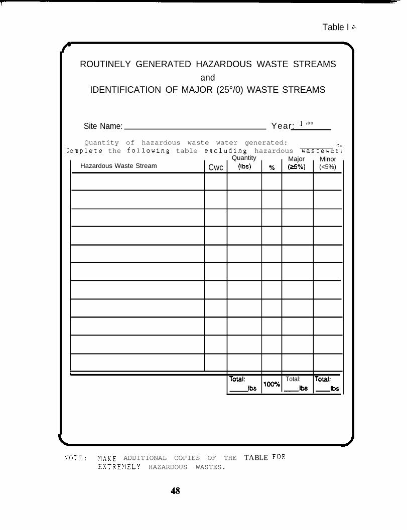
Table I ~
●
ROUTINELY GENERATED HAZARDOUS WASTE STREAMS
andIDENTIFICATION OF MAJOR (25°/0) WASTE STREAMS
Site Name: Year: 1 ’9 0
Quantity of hazardous waste water generated: 1-;omplete the followlng table excludlng hazardous waste~a:,
.>Quantity Major Minor
Hazardous Waste Stream Cwc (lbs) 0/0 (25%) (<5%)
tTotaL Total: TotaI:
hi ‘WA —Ibs —~
r
Y(3TE: )!AKE ADDITIONAL COPIES OF THE TABLE FOREXTRE?lELY HAZARDOUS WASTES.
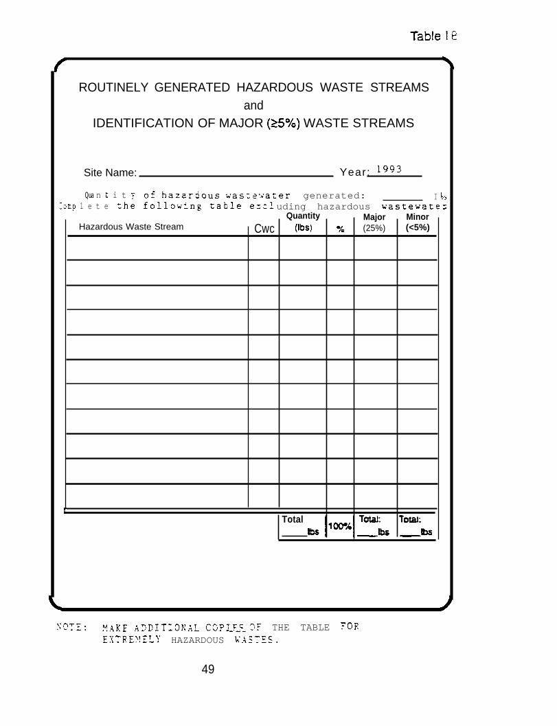
ROUTINELY GENERATED HAZARDOUS WASTE STREAMSand
IDENTIFICATION OF MAJOR (250/.) WASTE STREAMS
Site Name: Year: 1993
Qua n t i t y of hazaraous was:s’.~ater generated: I b~:omp 1 e t e zhe folloh”ing table ez:l uding hazardous wastewatez
Quantity Major MinorHazardous Waste Stream Cwc (lbs) ~ (25%) (<5%)
LTotal ToM:
—~
Y5’TE: .y.AKE ADDITIONAL COP~~~ OF THE TABLE FOR.-.EXTRE?!EL)’ HAZARDOUS L’ASTES.
49
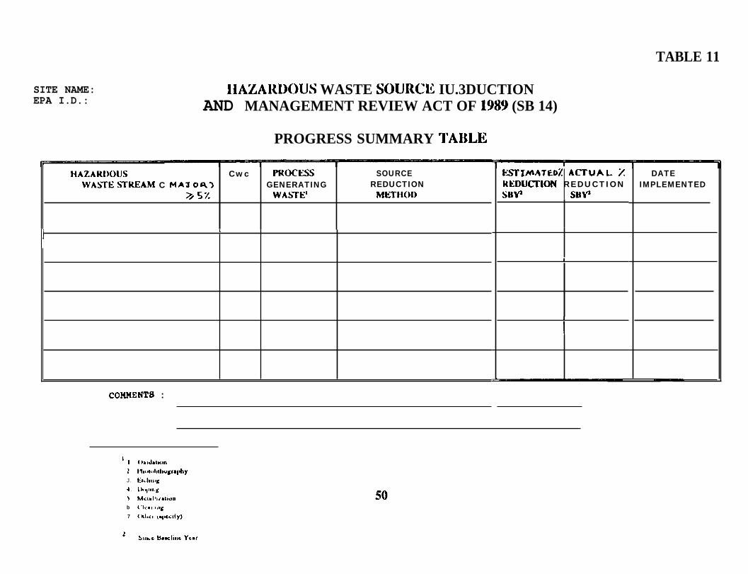
TABLE 11
SITE NAME:EPA I.D.:
1iAZARDOUS WASTE SOURCE IU.3DUCTIONAND MANAGEMENT REVIEW ACT OF 1989 (SB 14)
PROGRESS SUMMARY TABLE
HAZARIXWS Cwc PRoclxs SOURCEWASTE SrREAM C MAX OR> GENERATING REDUCTION
* 5X WASTli’ METIIOD
t1
CONMENTS :
IES’I’lMATEDZ ACTUAL zREDU(XION REDUCTIONSIlv Smv
,
1
I
‘11.J.
4.
>
b
7
t
DATEIMPLEMENTED

65
APPENDIX B
COMPLETENESS CHECKLIST

Source Reduction Evaluation Review & Plan Checklist
The following checuist may be helpiul in determining completeness oi a Hazardous Waste .+urceReduction Evaluation Review and Plan. The Department ot Health Services wiil be using a similarapproach to deterfie whether or not a review and plan has met the minimum requirements neces-sary to comply witi Of the Ha=rdous Waste Source Reduction and .Management Review .Act oi 1989.
1. Is your (the generator’s) name and address given in the plan?(CCR Section 67100-5(a)) JYes 3 No
2. Is the address the same location where waste is generated? Cl Yes J NoIf no, is there a given address where waste is generated? Cl Yes ~ No
3. Is the four digit SIC code(s) for the site given? (CCR S@ion 671005(b)) ~Yes J No
4. he you a small business? (CCRSection 671002(g)) Cl Yes J NoIf yes, is a DHS Waste Audit Study Checklist being usxi?(If yes, see Checklist for content requirements.) J’ies J NO
5. Is the plan addressing a multi-site operation? J Yes J NoIf yes. are all the sites’ addresses listed in the plan?(If no, this plan is incomplete.) JYes 2 h-o
e. Is t!!ere a description oi your business and waste generating activities in theplan? ~CCF. Section 671 OCL5C)) ~ yes J NO
1. Is the length oi time your company has been in operations at the presentsite provided in the plan? (CCR Section 671005(d)) J Yes J No
8. .&e the major manufactured products and semices you provide described inthe plan? (CCR Section 671005(e)) J Yes J No
9. Are the number oi employees working for you given in the plan?(CCR Section 671005(f)) J Yes J No
10. is there a general description of your operations in the plan?(CCR Section 671005(g)) J Yes J No
11. Does the plan identify all routinely generated hazardous waste streams whichresult from ongoing processes or operations having a yearly volumethat exceds five percent of the total yearly volume of hazardous wasteat the site? (CCR Section 671005(%)) 3 Yes 3 No
12. Dx+s the plan provide an estimate of the weight, in pounds, of wastegenerated at the site? (CCR section 671005(i)(l)) J Yes J No
13. Have you listed the applicable California waste code(s) for each wastestream? (CCR Section 671005(i)(2)) ayes J No
14. Are the waste generating processes, operatiom and activities (along withcorresponding diagrams) descnbd in the plan?(CCR Section 671005(i)(3)) JYes 3 No
s . IX the processes, opemtions and activities described inciude a listing of allinput materials contributing to the generation of waste?(CCR Section 671005(i)(3)) ~ Yes J No
—. . . .3ctober 1991 L-1 Checklists for the Plan, Report,
52 P lan Sumrnary and Report Summary

16.
17.
18.
19.
20.
71-.
23.
24.
25.
26.
Is there an evaluation or’ available source reduction approaches?(CCR Section 671005(j)) ~ yes J No
Do the evaluations for source reduction approaches consider inputchanges, operational improvements, production process changes,product reformation, etc.? (CCR Section 671005(j)) J Yes J No
Do the evaluations consider the following: (CCRSection 67100.5(k))
Expected change in the amount of hazardous waste generated? J Yes J No J N/ATechnical feasibility? 3 Yes a NO 0 N/AEconomic evaluation? J Yes 5 NO J N/ASystem capacity? 5 Yes 3 No Cl N/ASystem efficiency? JYes J No Cl N/AEffects on product quality? J Yes J NO Cl N/AEmployee health and safety implications? JYes J No 3 N/APermits, variances, compliance schedules ot’ applicable State,
Iocai and fderal agencies? 7 Yes J No U N/AReleases and discharges? JYes J No 5 N/A
Does the plan provide information, such as waste stream constituentand concentrations, pertinent to the evaluation of the source reductionapproaches? (CCR Section 671005(1)) J Yes 5 No
Is there a specification of, and a rationale for, each technically feasible and=onomically practicable source reduction measure(s) being proposedin the pian for implementation? (CCR Section 671005(m)) J Yes J No
Is there an evaluation and, to the extent practicable, a quantilcation of theeffects of the chosen source reduction measureis) on emissions anddischarges to air, water, or land? (CCR Section 671005(n)) J Yes J No
Is there a list of alternatives considered but not selected for a detailedevaluation as a potentially viable source reduction approach?(CCR Section 671 OO-XO)) J Yes J N’o
For each alternative rejected, is there a rationaie for rejection?(CCRSection 671005 (O)) 3 Yes Cl No
Is there a timetable/schedule for making reasonable and measurable progresstowards implementing and completing the selected source reductionmeasures? (CCR Section 671005(p)) JYes nNo
Does the timetable /schedule prioritize processes and wastes for futureresearch, development and source reduction analysis?(CCR Section 671005(p)) 5 Yes g No
k the plan properly certified? (CCRSection 67100.10) ~Yes CI No
&lists for the Plan, Report, L-2 October 1991ummary and Report Summary Ca

66
APPENDIX C
DETAILED INFORMATION ON SOURCE REDUCTION MEASURES

DETAILED INFORMATION ON SELECTEDSOURCE REDUCTION MEASURES
AQUEOUS WASTE
1)
2)
3)
4)
5)
6)
7)
8)
9)
Reduction of hydrofluoric acid using filtered/circulating etch bathsin a wet bench etch station (page 57).
Chemical efficiency comparison between a spray tool and a wet sink(page 59).
Wet sink bath life extension (page 60).
The Athens System - sulfuric acid reprocessing (page 62).
Ammonium sulfate solution hazardous waste elimination process(page 63).
DI water RO Unit upgrade and usage reduction (page 64).
Hydrofluoric acid, BOE, and Pad Etch reduction (page 65).
Installation of flow meters (page 66).
Improved controls on automatic feed system (page 67).
SOLVENT WASTE
1) Xylene backwash reduction project (page 68).
2) Reduction in the quantity of M-pyrol used (page 69).
3) Elimination of solvent contaminated water (page 70).
4) Using “dry” cleaning technology to replace “wet” cleaning(page 71).
55
STRIPPER WASTE
1) Substituted Nophenol 922 by EMT 400 stripper solution(page 74).
2) Used new stripper/rinse solution (page 75).
PHOTORESIST WASTE
1) Reduced positive photoresist usage (page 76).
2) Reduced amount of dispensed photoresist (page 81).
3) Switched from negative to positive photoresist (page 82).
SOLID CONTAMINATED WASTE
1) Administrative steps to reduce solid contaminated waste(page 84).
OZONE DEPLETING CHEMICALS
56
1) Ozone depleting chemicals (ODC) elimination project (page 85).
I

SGS-THOMSON (ST) Microelectronics. a word wide leader in modernmicroelectronics, has recognized the need to balance environmental concernsand economic growth. ST's Environmental Mission is to pursue all paths toeliminate or minimize the impacts of our processes and products on theenvironment, to maximize the use of renewable sources of materials and energyand to strive towards a sustainable development.
In late 1993, severai new wet bench stations were installed at the RanchoBernardo site. The new wet benches included filtered/recirculating etch bathsreplacing the static static baths. The new etch baths provide a cCSt effectivemeans to reduce chemical consumption while reducing particle counts.enhancing process control and improving procduct yield. This report focuses cr:he advantages of wng fiiterechc;rc:kting e[cn Sarhs cent.ainin~ nycrofiucr’cacia versus static etcb ba~hs.
DESCRIPTION OF ETCH BATHS
~
Wet bench stations original installed a[ the
IN A WET BENCH STATION
Rancho Bemardo site for wet etchingconsisted of two covered static acid etch baths (two and a haif gallons each), ?A6di-ionized rinse baths and a spin rinse dyer and sinK. To control etch rates ancminimize particle counts ‘he dip baths were arained 10 an on-site neumlizaticnsystem and then repoured with fresh ac:d. Th,e pcunng of fresn acic W=Sscheduled at a mimmum of once per day.
IN(7 FTCH BATHS
New wet bench stations were installed using high flow filteredkecircuiatingbaths.
1.2.3.4.5.
The filteredkecirculating e~ch baths have shown the following: -
Uniformity of etch ratesReduction in particle countsReduction in the number of acid poursReduction in the usage of hydrofluoric acidInoreased product yield
etcn
57
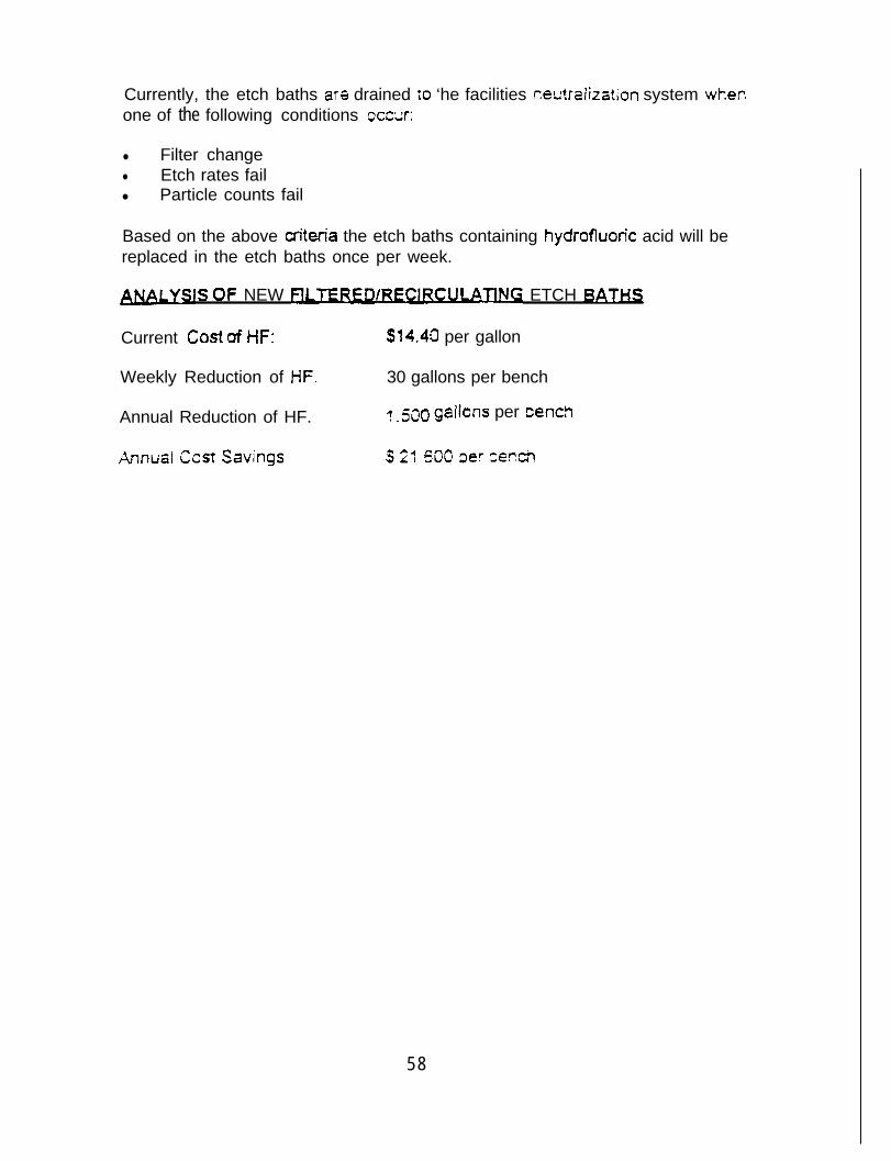
Currently, the etch baths ara drained io ‘he facilities ceutrelization system whenone of the following conditions occur:
● Filter change● Etch rates fail● Particle counts fail
Based on the above critm”a the etch baths containing hydrofluoric acid will bereplaced in the etch baths once per week.
5 OF NEW ~CULATlN(7 ETCH BATHS
Current Cost of HF: S14.40 per gallon
Weekly Reduction of HF: 30 gallons per bench
Annual Reduction of HF. ? .~~o gallons per ~ench
58

CHEMICAL EFFICIENCY COMPARISON BETWEEN ASPRAY TOOL AND A WET SINK FOR AN RCA CLEiUI
IN THE SUBMICRON DEVELOPMENT CENTERAT ADVA.NCED MICRO DEVICES, KNC.
In an &onto increase tool reliability, achieve a more repeatable, less problematic clean cycle and also toredum floor space rqtiements, spray tools were installed at the Subm.kron Developmem Center toperform the same predifTusion RCA cl-as a wet sink A wet sink is a chern.ical bath in which wafersare immened for the purpose removing oxide. The sink IM.5 a typical bath life of 3 hours with periodicspiking in order to maintain a constant etch mte and a uniform clean throughout the bath life. When theend of the bath life is reachetZ the bath is sent for neutitio% flushed with water, &h chemicals arepurcd and heated to temperature.
In contn% the spray tool does not immerse the wafer in liquid but tather uses a nozzle to spray multiplelots with a fixed chemical volume inside a closed chamber. Chemicals are not reused for another cleancycle. After use they are sent for treatment to the on-site acid neuualizan“on system prior to rel- to thePOT-W.
The qution was which tool used less chemicals and therefore operand more efficiently. To make anormal.ized comparison. chernicaJ efficiency was tnaluated on a volume used per wafer lot kis for thewet sink and the spray tool over a 24-hour rime period- Based on the a.na.iysis, the sptay tool uses h lesschemicals per lot than the wet sink. The chemicals evaluated included ammonium hydroxide.h)dmchloric acid and hydrogen peroxide. For all chemicals, the wet sinks used double the chemicalvolume per lot than the spiny tool, in some cases, three times the amount- In both tools, the chemicalefficiency is a function of throughput. That is, as the k“olume of wafers through the tool increases so doesthe chemical efficiency for cleaning the lots.
The reason for tis significant increase in chemical use can be attributed to many issues. Upon firstglance, one may have anticipated that the oppasite would be true because chemicals are reused for sevemllots, However, a larger chemizd volume is nad to M the bath. Also, because the etch rates decay as afunction of time, chemicals must be spiked into the wet sink bath in order to maintain a constantconcentmion. Spiking occurs regardless of wafer throughput bwer chemical efficiencies between runswere obsened as more pronounced when during a smaller wafer througJIpuL
For the spray tool, a smaller quantity of chemicals is used per ck.n. At maximum efficienqf, a spray toolcan run six lots sirnulta.neouly using one spiny volume. More lots per time cart be chnned with lesschemicals than the wet sink. BeJZM.W there is no chemical bat.k chemicals cannot evaporate and thereforedo not require spiking. A smaller volume of chemicals is used per lot for the spray tool RCA clean.
59

WET SINK BATH LIFE EXTENSION FOR RCA WAFER CLEANAT ADVANCED MICRO DEVICES,
SUBMICRON DEVELOPMENT CENTER
To i%cil.itate increased production in the Mision area in the Submicron Development Center(SDC) at Advanuxl Micro Devices in Sunryale, the wet sinks n&cled to have higher u Won ofthe RCA cleans (a tracMonal acid clean for wafers). Originally, the RCA cleans were used atSDC fix two hours and then duxnp@ flush~ repoured and re-hea.ted. The change-out proceduretook over au hour and complicated the diffusion area logistics. The goal of this project was tomod@ the baths to extend their I.× from 2 to 3 hours. T%e main limitation to the two hourbath M% was that the ammonium hydroxide (NH40H) in the RCA-1 bath evaporated out ofsolution and weakened the chemical strength of the bath. Lf additional chemical was addedperi~”cally, a process refkrred to as “spiking” the concentration was maintained In order to keepthe ammonia concentration constant in the RCA-1 cleaq spilGng of ammonium hydroxide wasimplemented. Over the course of the study, it was determined that the hydrochloric acid additions(HCl spiking) to the RCA-2 bath were not neces~. Ultimately it was determined througiI thetidy that hydrochloric acid consumption could be reduced by extending the bath Me for RCA-2.Ln both cases. the changes to the process enabled a constant ckanin g effectiveness during the entirebath life. The resultant modMcation to the process recipe resulted in a ovedl net increxe inchemical use at SDC. However, with the increase in sink up time, the chemical use efficiency overa fixed period of time also increased.
Ammonium hydrondeThe simplest way of monitoring chemical activity in the RCA-1 bath was to perform a clean andmwure the oxide lost on a test wafer. Experimental data showed that the etch rate decayedquickly over time if no additional ammonium hydroxide was added and thus reduced theeffectweness of the clean. In preparation for extending the bath life, samples of the chemical wereanal}zed for ammonia content. The etch rate w= supposed to remain constant over time,Experiments showed the rapid decay ofammoniurn hydroxide without periodic spiking. By spikingthe bath with ammonium hydroxide, both the oxide etch mte and ammonia content were keptrelatively constant. The original formulation of ammonium hydroxide with the addition of spikingresulted in too high of an ammonia concentmtion in the bath. This was due to the fict that thespiking ooxrred while the tank was bating to temperature. So the pour-up recipe was mod.if%d todecrease the initial volume of ammonium hydroxide added to the bath. The lower volume coupledwith spiking kept the concentration constant. The conditions of the RCA-1 tank were better usinga 3-hour lifetime with spiking than after 30 minutes elapsed time with spiking disabled.
Hydrochloric acidConversely, chemical analysis for hydrochloric acid on the RCA-2 tank just after pour-up, andthree hours dler pour-up showed that the HC1 concentration remained relatively axistant. TheRCA-2 tank did not need periodic additions of HC1. The same volume ofhydroehlonc acid nedxlfor the bixh could be used when the bath life was extended from two to three bours.
60

ConclusionBased on the new process, the chemical concentration of the RCA-1 and RCA-2 baths were heldconstant through out the bath Iifk by spiking the RCA-1 bath with ammonium hydroxide and byincreasing the bath I.if% of hydrochloric acid for the RCA-2 bath. The periodic addition ofammonium hydroxide kept the ammonia content and the oxide etch mte constant in the RCA-1bath. The three hour bath M% was klp]~ at SK.
It is diflkult to estimak the chemical reduction for anumxium hydroxide SiD(% dhOU@ bOthwafkr activities and ammonium hydroxi& use inc~ the bath Iif% was exten~ negating theneed to change out as fkpemtly. Despite the doubling of ammoni um hydroxide use, we achieved a50% increas in q“pmen! availability by extending the bath Iif% from 2 to 3 hours. The reductionin hydrochloric acid was more straight fbnvm@ hydrochloric acid use decreased by 25’%o byexkding the bath M%’.

The Athens System: Sulfuric Acid Reprocessing at Intel
As the world’s largest chip maker, Intel recognizes its standing in both industry
and the community as a role model. Intel also recognizes the value of a clean
environment. Thus Intel has taken a proactive stance to pollution prevention over the last
twelve years, aggressively pursuing source reduction measures in the last five.
In 1990, Intel used 743,091 lb of s-c in its produa”on processes in D2 and Fab
1, constituting 82% of the comosive liquid (CWC 135) waste stream generated in that
year. Obviously, this presented the greatest opportunity to make a large impact on wastegeneration at Intel. Recognizing this opportunity, Intel began in eariy 1993 to reprocess
sulfhric acid with the Athens system. The system enables tic acid used in the fid) tobe reused rather than treated in an Acid Wme Neutralization system and discharged to
the municipal wastewater treatment facility.
The Athens systems reprocesses used sulfhric in a three mep process. First, it
concentrates the used acid from the wafer process. The used acid is heated to 280”C.
boiling off water and other impurities to leave a highly concentrated (85?6 W) acid
solution. Second, it purifies the concentrated used acid through distillation. Finally, it
generates its own oxidant, peroxydisulfhric acid (PDSA), which has a higher oxidant
potential than the traditional oxidant, hydrogen peroxide. When combined with purified
acid solutioz this leads to an overall acid concentration of 92°/0, as compared to 80-80°/0
when hydrogen peroxide is used. Reprocessed acid is then pumped back into the wet
stations in the fab for continued wtier processing.
The Athens system is notable for several reasons. Strict purity requirements of the
semiconductor industry make chemical reprocessing a challenging prospect. Sulfhric acid
reprocessed by the Athens system is actually of higher quality than new sulfbric in drums.
While the system benefits the environment by reducing the volume of hazardous waste
generated, it benefits Intel as well by saving money. The system processes about 64o9
gallons of sulfhric acid per week The aUKIUa.1 savings from foregone sulfuric acid
purchases alone is approximately S2.9 million. Further savings are obtained through areduced load on the Acid Waste Neutralization system.
The effect of the Athens system on Intel’s hazardous waste generation has beensignificant. In 1993 Intel generated only 208,824 lb of sulfuric acid waste from fabprocesses, 28% of the amount generated in 1990. This reduction was obtained despitean increase in production over the same period of at kast 25%”(a ccm.sctvative estimate,as processes become more complex and wafer sizes change). Furthermore, the higher
quality sulfbric increases die yields.
The Athens system provides the best of both worlds: it reduces waste and saves
money. The success of the system has insured its integration into all fiture Intel fabs.
62

Ammonium Sulfate Solution Hazardous Waste Elimination Process
Backcjround:Ammonium sulfate solution, generated from an ammonia removal process operating at the NECElectronics Inc. (NECEL) waste water pretreatment plant, had .to be disposed of as a hazardous wastedue to consistently low pH (< 2). The ammonia removal system was installed in 1989, following newmandate from City of Roseville requiring NECEL to lower ammonia levels in the pretreated waste waterdischaqe to the POTW.
The ammonia removal process is a batch opemtion, during which ammonia laden air generated from airstripping of segregated stream of production waste rinse waters, is treated through a sulfuric acid(HZS04) scrubber to form ammonium sulfate solution. The original ammonia removal system utilized amanual acid (H#OJ fill procedure, which was ve~ time consuming and inconvenient. Consequently,the acid was not efficiently used and the resulting ammonium sulfate solution which was of varying pH,typically <2, had to be shipped off site for disposal as a hazardous waste.
Actions Taken:Follow”ng the source reduction review (mandated under SB14) undeflaken in 1991, the ammoniumsulfate waste was identified as a major hazardous waste source. M is commonly known that ammoniumsulfate solution, at neutral PH levels, is a nonhazardous material typically used as a feedstock forfertilizer manufacturing process.
During 1992 the following improvements made to the ammonia removal system to render the resultingammonium sulfate solution nonhazardous:
● Controls were added to automate (based on PH level) the H&04 refilling process.● To assure the HZS04 is efficiently used up, procedures were developed and implemented by
Facilities Engineering that require operators to conduct sample verification and to test ammoniumsulfate concentration and pH prior to transferring the ammonium sulfate solution to the final storagetank.
● Back up pH controls were added to the final ammonium sulfate storage tank fill line, which will notallow the tmnsfer of nonconforming ammonium sulfate solution.
● Specifl=tions developed by Facilities Engineering require that operators complete and maintaindocumentation for each batch of ammonium sulfate solution transferred to the final storage tank.
● The neutral ammonium sulfate solution was tested per Title 22 and determined to be anonhazardous material. This test is voluntarily repeated every six months.
. A contract to supply nonhazardous ammonium sulfate solution as a feedstock for fertilizermanufacturing process was prepared initiated in November 1992.
Current Status:Recently, an innovative on-site reuse of the ammonium sulfate solution, to feed the vitrification colon~nat the new waste water treatment plant was identified and confirmed. To start up this process, newequipment has been purchased and installed. The on-site reuse will generate additional savings byeliminating purchase of bagged ammonium sulfate, Aiti is currently used to feed the vitrificationcolony.
n me nW waste water tmament plant utilizes a biological treatment process (nitrificdion colony)for removal of ammonium ion from the new production facility waste rinse waters. The vitrificationbacteria require a steady level of ammonia to thrive and to peflorm at required levels. Currentlybagged ammonium sulfate is used to eliminate any variation in incoming ammonia levels, Liquidammonium sulfate will replace bagged solid ammonium sulfate.
Savinqs:Annual savings are estimated at approximately $120,800.
63

SOURCE REl)Uff IOH WURB ATAN?kLOG DEVICES
PI Water RO U~ Reduction. .
Reverse osmosis f51ters and mixed bed ion exchange columns are two majorcomponents of ADI’s purified water systin Mixed beds work by removingM @~es (ions) f%m the water. The beds are fiIIed with anionic andcationic resin beads. As these beads load up with paticles they lose their ionexchange capacity and must be regenemted- This is done by flowing ametered stream of Sulfiu-ic Acid and Sodium Hydrotide, which strip off thepa.rticIes.
The frequency of regenerations is dependent on the quality of the feedwatir (measured in titd dissoIved soIids or TDS) and the toti gdons flowedthrough the bed. Reducing either the total gallons or the TDS will result inless regenerations and Iess chemical use.
The water flowing to the tied beds comes &om the reverse osmosis(RO) systwD- The RO removes &SSOIV~ sofids by forang water through asemi-pmneable mem.b=e at high pressures. This creates kvo fluid streams,the product and the concentrate. ‘The product is sent b the mixed beds. Theconcentrate is sent to d-rain or reclaim. The efficiency of the membranes ismeasured by the percen~ge rejection of TDS:
= % RejectionFeed Watir ~S
We replaced our old Cellulose Acetati membranes with new highefficiency Thin-Film Composite membranes. The resulting drop in TDS in theproduct stream had a direct effect on our regeneration frequencies andchemical use. In addition to satig chemicals we saved considemble amountsof purified water that is needed @ the regeneration process. Ln all there wasabout an 80% reduction in water and chemical usage.
Before RO UDmde r RO Un~deM?en.eration.s rm w e e k 4 0.8Witerused - 40,000 gal 8,000 galSodium Hydrotide 400 gal 8ogdSdfhric Acid 240 gal # g a lTDs 8s ppm 13 ppm
64

SOURCE RBDUCrIOM MXASURE AT~ DBV?CXS
rofluoric Ac+d. BOE QLU-EMI?&hIIafivtircdation 1 &tration baths were installed and modifications were done oncertain equipment. Teflon blocks were installed in sinks b reduce tie volumeof chemic~. Due to IOW usage of some sinks, the bath change frequency wasextended. For BOE 20:1, the change frequency went born twice a week toonce a week (a 507c mdufion for this sink).
In 1991 we began plans for our Hyd.rofluoric acid treatment system. Thissystem was i.nwnded to reduce the volume of hydrofluoric acid that we hadbeen shipping oiT-tite. In June, 1992 the system WaS completed and we beganprocessing batches of ~ waste. With the addition of Cahum chioride.-Magnesium hydrotide, and a poiyner, we were able w get the Fluoride coflock out of the liquid and combine with Ae CaIcium to produce Caiciumfluoride siuage. This sludge is coilecwci within a 90 day ~eriod and thens tipped ~fi-si~e. ‘we no longer trans~~r. :<ycirodumic ~~.a oil’-si~e 5-inC9 ‘wehave ~he capa~~ty ‘m crea~ ail ~f our --- Wasu tiTA Li-us sys-zem.
i992 ‘Hydrofluoric acid haulou~s 226.076 gallons1993 [email protected] acid haulouts 67,673 gallons1993 Calcium fluoride sludge W yards1994 Hydrofluoric acid haulouts f) g~]ons1994 Calcium fluoride sludge ~y vards (to date).
65
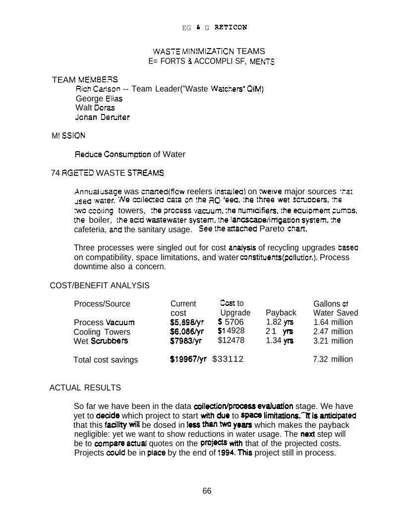
EG & G RZTICON
WASTE lMlNlMlZ4TiON TEAMSE= FORTS & ACCOMPLI SF, MENTS
TEAM MEMBERSRich Carlson -- Team Leader(”Waste Walche& QIM)George EiiasWalt Dor=Johan Demiter
M! SSION
Reduce Ccmsumption of Water
74 RGFtD WASTE STRE4MS
Annual usage was chaned(fiow reelers insiaJleo) on tweive major sources ~h~i
~~~a w~ler. ‘~e ~lJ~ea c~ta an the Ho fe~, :he ;hree We? :~o~ooe~, :~e
WO caoiing towers, ?he prccess waum, :he numicifiem, fhe equigmem ;umos,the boiler, ~he acid wastewater system, the kmscape/irrigation sy~em, :hecafeteria, and the sanitary usage. See the attached Pareto chafi.
Three processes were singled out for cost anafysis of recycling upgrades oaseaon compatibility, space limitations, and water ccnstituents(pollutiorl). Processdowntime also a concern.
COST/BENEFIT ANALYSIS
Process/Source Current cost tocost Upgrade
Process Vacuum $5,89~r $ 5706Cooling Towers S6,086/yr SI 4928Wet Sabbers $79631yr $12478
Total cost savings $19967/yr $33112
ACTUAL RESULTS
Gallons ofPayback Water Saved1.82 yrs 1.64 million2 1 yts 2.47 million1.34 yrs 3.21 million
7.32 million
So far we have been in the data collectiotipfocess evaktion stage. We haveyet to decide which project to start with.due to $paoe limitations.Tis antiapatedthat this faciWy w“il be dosed in less tim W ye~ which makes the paybacknegligible: yet we want to show reductions in water usage. The nexl step willbe to compam a~u~ quotes on the pfoja ~h that of the projected costs.Projects could be in place by the end of 1994. ~is project still in process.
66

EG & G FLETICON
WASTE MI NIMIZA7:ON TEAMSSF FORTS & ACCC MF LIS+I ME NTS
TEAM MEMBERSRichard Carlson George E!iasWait Doras Johan Oeruiter
MISSION
Reduce the co& Vconsumption of cnemicais required to treat the acidwastewater which flows into our acid neumdization system.
TARGcHED WASTE STREAMS
Volume of sodium hydroxide, and :he amcum of sulfuric acid used IO aa@ :hean Of ~1 wastewa~ers wmch flow from cur ‘arica~ion areas ;mo cur on-sne,
wasewaler :reaImenl Svslem ‘Cr :reamem Dnor :C aiSCnar~e:0 :he iccsI ‘VW.
CC ST, ”6ENE~!T ANALYS i S
Sulfuric SodiumAc~d Hydroxide Total Costpounds pounds per year
1992 10,035 49,384 $68501993 1 5 , 5 2 4 66,745 $9522:$94 4 , 0 2 0 49,384 (projected) $6042 Savings of 360/~ in W.
Froauction(wafer stans) has increased 60% since base line 1992.
Ra~her than adding a third setiing tank or modifying for an dtemative causvc,like magnesium hydroxide, we concentrated on better maintenance and under-standing of the acid wastewater system. We experimented with aJtema.tWeset controls on the automatic feed system, we documented daily inspections, wecalibrated and deaned the probes Weetiy and we controlled size of fabdumps in oder to establish better operating controls for the system. The AWNnow uses less additives for ph control. We can now avoid the ping pong effectwhich wasted chemicals. our system is small with only a 10 minute retentioticycle time per tank
ACTUAL RESULTSThe acid neutralization system is operating more effiaently and requiresless maintenance than before. Facility maintenance techs really didn’tundemtand the system so we had to retmin oumelves. There are to manyvariables to operate a perfect system.
67
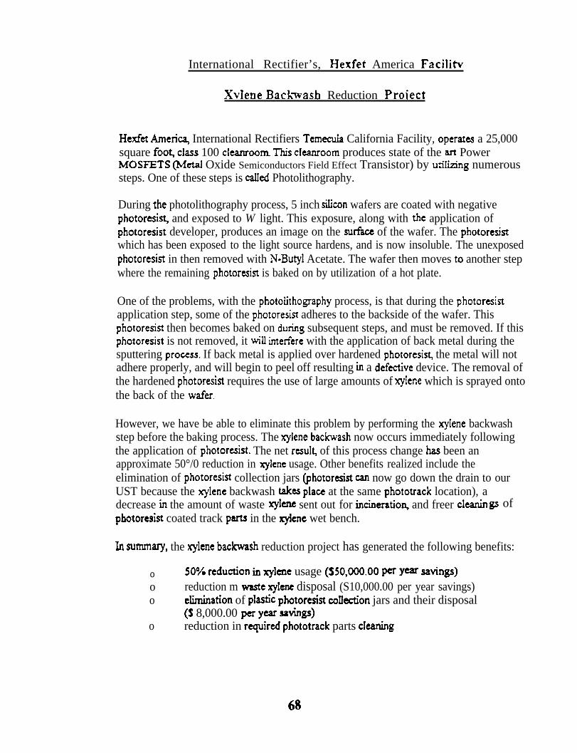
International Rectifier’s, I-Iexfet America FaciIitv
~~’lene Backwasb Reduction Proiect
Hetict kneri~ International Rectifiers TemecuIa California Facility, operat~ a 25,000square foot class 100 ckanroom Tlis cka.nroorn produces state of the w PowerMOSFETS (Metal Oxide Semiconductors Field Effect Transistor) by utiIizing numeroussteps. One of these steps is cakd Photolithography.
During the photolithography process, 5 inch silicon wafers are coated with negativephotoresisg and exposed to W light. This exposure, along with the application ofphotoresist developer, produces an image on the surfkce of the wafer. The photoresistwhich has been exposed to the light source hardens, and is now insoluble. The unexposedphotoresist in then removed with N-Butyl Acetate. The wafer then moves to another stepwhere the remaining photoresist is baked on by utilization of a hot plate.
One of the problems, with the photol-ithogaphy process, is that during the photoresistapplication step, some of the photoresist adheres to the backside of the wafer. Thisphotoresist then becomes baked on during subsequent steps, and must be removed. If thisphotoresist is not removed, it will inteflere with the application of back metal during thesputtering pro=ss. If back metal is applied over hardened photoresis$ the metal will notadhere properly, and will begin to peel off resulting in a deftiive device. The removal ofthe hardened photoresist requires the use of large amounts of xylene which is sprayed ontothe back of the wafkr.
However, we have be able to eliminate this problem by performing the xylene backwashstep before the baking process. The xylene bachvash now occurs immediately followingthe application of photoresist. The net resd~ of this process change has been anapproximate 50°/0 reduction in xylene usage. Other benefits realized include theelimination of photoresist collection jars (photoresist can now go down the drain to ourUST because the xylene backwash taks pla~ at the same phototrack location), adecrease in the amount of waste xylem sent out for inci.neratioq and freer cleanin gs ofpbotoresist coated track pm in the @ene wet bench.
Lrt summq, the xylene bachvash reduction project has generated the following benefits:
o 50~0 redution in qkne usage ($50,000.00 W Y- ~v@V)o reduction m wsste xylene disposal (S10,000.00 per year savings)o ehination of pkstic photoresist ccdlect.ion jars and their disposal
($ 8,000.00 ~ y~ wings)o reduction in requkexl phototrack parts ckaning

Intel Corpomtioo! 900 Pnunc Citv RoadFoisom. C.+ 95630 -9!99
19 16) 356-8080
aIntelPauline BatanehDepartment of Tome Substances ControlOffia of Polhmon Prevennon and Technology DcvelopmcmP.O. Box 806%cra.rnenm, Ciz 958124806
.%.l~L !0. 199A
SURJECT: HAZARDOUS WASTE REDUCTION MEASURE
Y@Tol (N-.Medsyi-~.-gyrrolidone) is a soivenr .dxu IS w by ‘h Son op~~on r~ .ymm,e ~ fim ,~etice 01- marked wafers 3ruslIed wafers .mme ‘m Foisom ium mher Intei sues These wa.ren muan-he die from w!mcit t-he M mlegnued curu 3 ?roaured and Lhe.z can be me: ~00 die on ury q~’e~waxer, :ach die mum be xamal.lv msmd for 3nv &=eCI ‘dMN mud have OKJITH Wring 2onc3non.
When ti-ects are found. hat pamcuk iie IS marked w-h I am oi ink to :riemfy ~hI I :s aeiecztve. YLhe wafer is to be reused. r-he mk must be removed. M-yroI ,removes ‘he ti Wltiou.r ?@’nuilv oreiecmical.ly harming the Op?mDOtd die on the wafer,
The overall reduction is due primarily 10 tie solvent being changed on an as needed bass msm.ad ofrouuneiy. TMs meant ptRhtniMQ’ UN.@ 10 ensure fewer m-pyrol changes would not a.rkr ‘theoperational die and changing the process spet%tions that had been in place for some ume. in addinonto changing the m-ptyol rinse bath less often. only one permn has been @en access to the sranon forwafer clean.in g. The srarion has a satellite drum for m-pyoi collection and it is mounted With a drum lockso unauthorized persons cannot access iL .ln inkless produre is LO the proms of being dm.eloped andproliferated throughout the corpmtiom The updated son procaiure W nack tie A-ecmfe die by theirspecitic ltion on the wafer it5elf so Lhey W no longer need to “m marked wILh mk ana dserefom. wdlnot need to be cleaned The coordinates oi the defecnve die 3re ‘hen stored on a floppy di*erte r+il Muchtravel with the wafer.
Usage of m-pyroi has chopped fim 101 .dom M igg~ to id ga.iloIIs “a 19$’3 wiucn reduced -be a.moumof waste to lx shipped off-site which then reduced b cost m-waste disposal tim about S1.500.00 in 198-to S250.00 in 1993. In additiotL the pudasing cost has dqped horn S2.626.00 in 1987 to S279.00 m1993. These Rchlced rmmbers also RsllIt in less maurial handling which m turn reduces the potentd forspills and 1* and immascs the safety for employees handltn“ g the material.
If you have any qucshons or need any tier mformauota PI= ~ me a call aI 356-5462.
Barbara BOS
Environmental Coortitor
.ti EquaJ OPPO~mV E~PIOVer 69
, / WG 1 8 t994

INTEGM4TED DEVICE TECHNOLOGY
Elimination of Solvent Contaminated Waten
The project entailed using carbon adsorption to remove the orgtics from our rinsewaters. The carbon adsorption bed was hard plumbed directly into our process whichinvolved equipmenl pip@ and Iayout changes within our process.
In preparation for using tbe carbon the fblIowing source hxhxtion measures wereund~ The entire project took 2 years to complete.
1. InDut Material ch~ Acetone was dmi.nated from the process and isopropyialcohol was substituted (Acetone is not removed by carbon adsorption)
2. InDut Material Cha.ues To eliminate all ozone depieting ch-”cals from alI of ourIDT sites 1,1,1 tricldoroetha.ne was Ani.nated and a terpene soive.nt substituted.
3. Inuut Matm”ai Chanszes and Process Change: Vapor degre=ing wkh Freon-1 13 WMeliminated and replaced with an aqueous water rinse. Repiacing the vapordegmzsing tith a m.ter rinse involved changing the process.
4. Ati”nimative Procedural Mea-sures: Documentation reflecting the change in whichthe process was being pefionned was generated.
The project resulted in the following benefits:
5. Jleduction of Hazardous Waste: No hazardous waste from this process has beinggenemted since implementation on March of 1994. Has resulted in 100%elimination of our solvent contaminated tie water.
Prior to implementation of carboq generated 1O-55 gallon drums of solventcontaminated water (4,587 po~ck) every 90 days.
6. cost Saving: Cost saving rezdized for second quarter of 1994 w s4,900 fortansportiition and disposal.
Estimated annual saving of approxkndy S20,000.

Plasma Dry Cleaning of Wafers
Gary S. SelwynPhysics Division, Los Alamos National Laboratory
Los Alamos, New Mexicoand
Department of Chemical EngineeringUniversity of California, Los Angeles
Los Angeles, California
Background
Materials required for microelectronics manufacturing areextremely sensitive to the presence of dust particles in the sizerange of 0.2#m and larger. Particles reduce the product yieldand cost-efficiency of the product and also can similarly reduceproduct reliability. To minimize these influences themicroelectronics industry employs a broad base of controls aimedto preventing particle contamination such as vacuum processing,cleanrooms and dust-free garments for workers. Despite the besttechnology employed in particle prevention, cleaning of wafersand photomasks is also required and is extensively employed.Even with this two-pronged approach, particle contamination stillaccounts for more than 50% of product yield loss with a financialimpact to US industry in excess of $lB/yr.
Beyond the direct cost of yield and product quality loss due tocontamination, the current technology requires the use of largequantities of chemical solvents and inorganic acids. Thesestand-alone llwet-stationsi’ require cleanroom space, chemicalmonitoring, replenishment and waste disposal. Additionalindirect costs involved in wafer cleaning include transportationof the solvents, safety issues in storing, transporting anddisposal of the chemical solvents and the cost of monitoringthese chemical stations and the workers.
Preliminary studies have shown that spent organic solvents andacids, generated in cleaning and etching operations, dominate thewaste inventory in semiconductor fabrication (CaliforniaDepartment of Toxic Substances Control, 1994). Organic solventsare volatile, making them a significant exposure risk to workers.Also, organic solvents leaking from storage tanks have causedgroundwater contamination. The use of acids, particularlyhydrofluoric acid, presents a major occupational and publichealth risk. The risk associated with HF usage is so seriousthat the South Coast Air Quality Management District inCalifornia requires users to relay continuous emission datadirectly to the regulatory agency. The semiconductor industryrecognizes the major risks associated with the use of thesechemicals and is seeking new technologies for cleaning andpreparing semiconductor components.
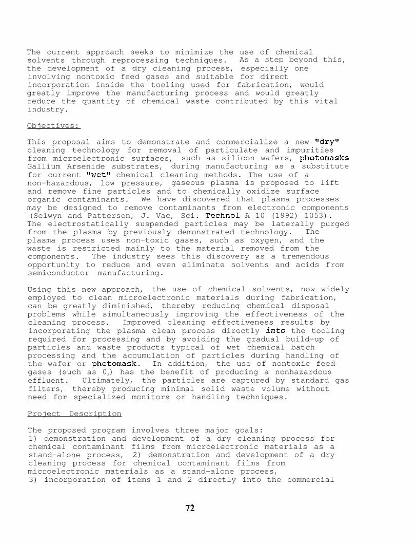
The current approach seeks to minimize the use of chemicalsolvents through reprocessing techniques. As a step beyond this,the development of a dry cleaning process, especially oneinvolving nontoxic feed gases and suitable for directincorporation inside the tooling used for fabrication, wouldgreatly improve the manufacturing process and would greatlyreduce the quantity of chemical waste contributed by this vitalindustry.
Objectives:
This proposal aims to demonstrate and commercialize a new ‘dryNcleaning technology for removal of particulate and impuritiesfrom microelectronic surfaces, such as silicon wafers, photomasksGallium Arsenide substrates, during manufacturing as a substitutefor current ‘wet” chemical cleaning methods. The use of anon-hazardous, low pressure, gaseous plasma is proposed to liftand remove fine particles and to chemically oxidize surfaceorganic contaminants. We have discovered that plasma processesmay be designed to remove contaminants from electronic components(Selwyn and Patterson, J. Vac, Sci. Technol A 10 (1992) 1053).The electrostatically suspended particles may be laterally purgedfrom the plasma by previously demonstrated technology. Theplasma process uses non–toxic gases, such as oxygen, and thewaste is restricted mainly to the material removed from thecomponents. The industry sees this discovery as a tremendousopportunity to reduce and even eliminate solvents and acids fromsemiconductor manufacturing.
Using this new approach, the use of chemical solvents, now widelyemployed to clean microelectronic materials during fabrication,can be greatly diminished, thereby reducing chemical disposalproblems while simultaneously improving the effectiveness of thecleaning process. Improved cleaning effectiveness results byincorporating the plasma clean process directly into the toolingrequired for processing and by avoiding the gradual build-up ofparticles and waste products typical of wet chemical batchprocessing and the accumulation of particles during handling ofthe wafer or photomask. In addition, the use of nontoxic feedgases (such as 02) has the benefit of producing a nonhazardouseffluent. Ultimately, the particles are captured by standard gasfilters, thereby producing minimal solid waste volume withoutneed for specialized monitors or handling techniques.
Project Description
The proposed program involves three major goals:1) demonstration and development of a dry cleaning process forchemical contaminant films from microelectronic materials as astand-alone process, 2) demonstration and development of a drycleaning process for chemical contaminant films frommicroelectronic materials as a stand-alone process,3) incorporation of items 1 and 2 directly into the commercial
72

tooling commonly used in microelectronics processing. Items1 and 2 are short term goals of 1 year or less. Item 3 is along-term goal intended for completion in year 2000. It shouldbe noted that the necessary element of this program involves anovel aspect of plasma processing not previously disclosed orutilized in any commercial product. The project involvesindustry partners for commercialization of the tooling and forevaluation of the product effectiveness. Development of the basetechnology is shared primarily between LANL and UCLA withinvolvement and monitoring by the industry partners. Oneindustry partner will build the plasma cleaner for wafers andphotomasks. California industry partners will evaluate the useof the plasma cleaning technology for use with photomasks, Siwafers and GaAs substrates. An important differentiation of thisprogram from conventional and competing approaches is that thistechnology is designed to clean patterned wafers with fine-linestructures without damage to delicate device structures andwithout the use of chemical solvents. Instead, a low pressure,nontoxic and unreactive plasma is used to neutralize the chargeof particles on the surface and inside device features. Theplasma also lifts and suspends the particles, greatly simplifyingtheir collection and removal using previously methods previouslydeveloped by this group. This work will be developed atLos Alamos National Laboratory (Gary Selwyn), in collaborationwith UCLA.
The second project task involves developing a plasma cleaningtechnology for removal of organic contaminant films onmicroelectronic surfaces, particularly photomasks, Si andGe wafers, and GaAs devices. This work will be performed byGary Selwyn and Robert Hicks at UCLA. The optimum plasma reactordesign and operating conditions will be identified forcontaminant removal from each material, while at the same time,minimizing the environmental and health-risk effects. Inaddition, a preliminary assessment of the plasma tool forincorporation into device manufacturing will be obtained.Devices will be prepared at UCLA and their performance assessedat the industry partners. The product of this task will be adesign prototype for use in constructing the commercial plasmatool. At this time a plasma producing high concentrations ofmetastable, singlet 02 will be developed as the active cleaningmedium.
Finally, in the third task, the particle cleaning process will bemerged with the chemical cleaning process to produce a singlestep cleaning process to serve as a substitute for many wetchemical processes currently being used. The reduction inchemical waste will be quantified by stream input and outputstudies conducted by UCLA (Prof. David Allen) at Californiasemiconductor and photomask industries. The improvement in waferor product cost will be similarly quantified.
Gary Selwyn may be contacted at (505) 665-7359; Robert Hicks maybe contacted at (310) 206-6865, and David Allen may be contactedat (310) 206-0300.
73

EG & G RETICON
WASTE MINIMIZATION TEAMSEFFORTS & ACCOMPLISHMENTS
TEAM MEMBERSSteve Ogden Carol RheinLinda Jansson John Cummings
MISSIONTo reduce the cost of off-site waste disposaJ(Hazardous W@te).
To find a replacement for Nophenol 992 Photoresist Stripper a chemical thatis costly to dispose of as a hazardous waste, and a replacement that would be~xempt from cefiain restrictions on organics per our permit with the BAAQMD.
TARGETED WASTE STREAMS
Nocnencl :22 SViOoer usea n ‘ab and :hlnning ~ab arocess(fcur resewcirsj
GCST’EENEFiT ANALYSIS
The engineers evaluatedflested multiple organic compounds that hada higher boiling point which would be exempt from BA4QMD permitconditions and chemicals that wouid not have to sent off-site for costlydisposal as a hazardous waste.
EMT400 was the chemical found to be a suitabie replacement which could5e disposed of on-site and was exempt from BAAQMD permitted emissions.
E.MT 400 is more expensive as a virgin chemical, but will save the timeilaborCCSIS previously required to handleiprepare the waste for off-site disposai.
Name Unit Cos# Annual Waste Disposal TotaJUsage
EMT400 Stripper 399x$38922 Nophenol 399x$26BAAQMD upgrade(NophenOl
FImt Year Savings
ACTUAL RESULTS
cost CosVLabor cost$15,162 0 $15,162$10,374 !$4788 $15,162
sinks if we don’t switch to EMT 400) $2,700
$2,700
EMT 400 Stripper has now replaced the Nophenol 922 strip process in fab.Em 400 evaluation to replace Nophenol 922 in thinning lab is still in process.This project was completed on August 23, 1994.
74

SILICON SYSTEM SOURCE REDUCTION PROGRAM
2 CASE EXAMPLES
David PaisAugust 26,1994
As part of our environmental program, Silicon Systems Inc. iscontinually looking for new ways of chemical source reduction andhazardous waste minimization. Source reduction measures includeemployee education, chemical substitutes, and new production methods. Ourmost recent source reduction measures have been the replacement of ourphotoresist stripper and rinse, and plans to reduce photoresist usage,
Photoresist StripperWe have switched positive photoresist strippers to a product with
extended use capabilities. With this new stripper material, we are able toextend the bath life, and increase the number of wafers per bath. This isexpected to reduce our usage of shipper by 50%. The new rinse will replace
isopropanol (IPA) in the rinse process, reduang usage of IPA by 75%. In
addition to reducing waste, the new rinse is also a safer alternative to IPA byreducing the fire hazard.
Photoresist ApplicationThe application of photoresist is dependent on the speed at which the
~’afer is spinning during application. We are currently testing different timesof application to determine if less chemical could be used on each wafer. Ithas been proposed that by reduang the application time for each wafer, the
amount of photoresist applied could be reduced by almost 50% without
sacrificing product quality.
Production demands in the semiconductor industry make sourcereduction an extremely challenging task. Every major process changerequires engineering qualification to ensure product quality and reliability aremaintained. By exploring new chemicals and processes, SSi has been able to
significantly reduce generation of hazardous ~’aste, and hopes to continue
this trend in the future.
75

FROt : I=li?CH/pLNG & ENU DE=T. TO : 916 227 4 4 9 4 1994 ! 09-02 17: 21 8651 P.02/05
LS! Logi:Corpontioc LSI
15i)l McC3rIhy BlvdM I IPIMS CA 95035
408.4338000
Sept=mber 2, 1 9 9 4
Paul ine BatareshDepartment of Toxic Substances C o n t r o lOff ice of Pol lut ion Prevention and Technology Development301 Cap i to l Ma l l , I s t F loorSacramento, CA 95814
Dear Ms. Bataresh,
LSI Logic Corporation has beeri using our Qual i ty Improvement Systemas an administrative approach to source reduction. Q u a l i t yImprovement Meet ings (GIM) provide a formalized structure ands y s t e m a t i c process for department groups to ident i fy and el iminatedefscts. T h e use of more chemica l t h a n r e q u i r e d in a process w a si d e n t i f i e d as a de fec t and ass igned to spec i f ic QI14s.
I have attached a d e s c r i p t i o n o? one Cycle of Guality ( a t t a c h m e n t 1 )c o m p l e t e d by our Milpitas Fab which focused orI reduc ing pos i t ivephotoresist usage. They were able to reduce monthly resist usagef rcm 41 gal lons to only 1 gal lon. Our Santa Clara Fab QIM comple teda similar cycle which is described in our employee newsletter(a t tachment 2 ) .
T h e same a~proack was used to reduce phosphor ic and su l fu r ic ac idusag= in chemical process baths. T o ensure low par t i c le counts andminimize contamination, chemical baths were changed very often.Phosphoric Acid usage was reduced 80% when internal studies showedthat changing a ba th when the par t ic le count was 50 instead of 2Ccould be accompl ished withuut affect ing product qual i ty . Phosphoricacid bath life was extended from S hours to one week.
Sulfur~c acid usage was reduced 60 % by decreasing the bath 6ize,consolidatifi~ opera t ions and ex tend ing the bath life from four hoursto eight hours. Refer to attachment 3 for more detai ls .
I would be glad to discuss these source reduct ion measures fu r ther .Please contact me at (408) 433-4210 if you have any q u e s t i o n s .
S incere ly ,
Linda GeeEnvironmental Fianager
76
e n c l o s u r e s
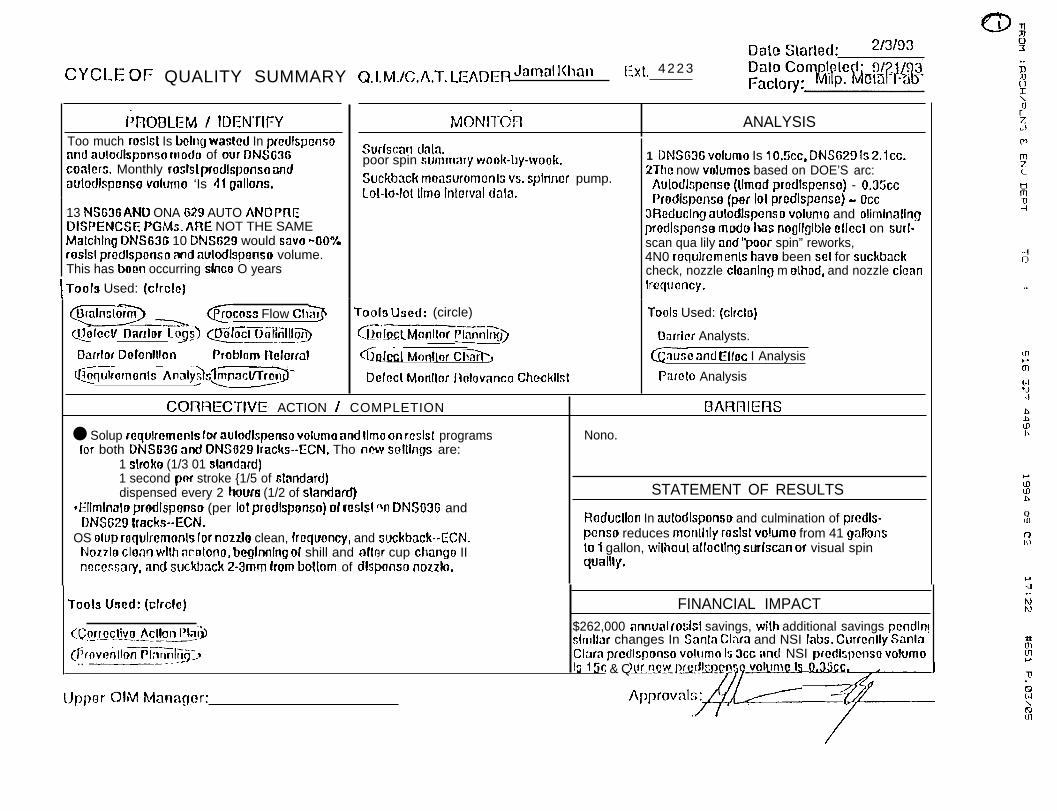
CYCLE OF QUALITY SUMMARY Q.l,M./C,A,T. LEADER ‘amat ‘(llall~x[t 4 2 2 3
fi70BLEM / ummwToo much roslst Is beltlg waslcd In pwdlspcnsormcl aulodisprmso modo of our DNS63CJCO~!CfS. Monthly fOStS! (XO(ihj)OflSO d
aulodlspenso vohrmo ‘Is 41 Qallons.
13 NS636 ANO ONA 629 AUTO AND PREDISPENCSE PGIW. ARE NOT THE SAMEMalchlng 0/4S636 10 DNS62!J would savo -00%roslst predlspenso nnd aulodlspenso volume.This has bocn occurring slrrco O years
I Toofs Used: (cfrc!c)
Da(c Slarled: 2/3}93
MOW-OR ANALYSIS
Sudscan dala. 1 DNS636 volumo Is 10.!icc, DNSWJ Is 2,1cc.poor spin sunlnlary WOOk-ily-WOOk.Suckback moasuromcnls vs. splnnor pump.
2Thc now vokrmos based on DOE’S arc:
Lo!-lo-lol tlmo Inlcrval clala.Aulodispcrrsc (Ilmad prodlspcnsc) - O.WiccPfodispcnso (per Iol prcdlspcnsc) - Occ
3Reduclng mrlodlspenso volumo and olimfrlalingprodlspcrnse modo has noglfrjbie ellccl on surl-scan qua lily and ‘“poor spin” reworks,4N0 roqulrcmenls have been sel for suckbackcheck, nozzle cioanlng m olhod, and nozzle cicanIrequency.
@iiEEE2... cProcoss Flow Char Tools Used: (circle) Tools Used: (CkCtO)
Qofccl! Dafrior Lo~~> @tilfi~71iWi6@ <~o~~L/@nllor f~n;hi Oa.rrirx Analysts.Darrfof Dolonlllon Prablorn llclorml 6Q!CGI A40nllor CIEFPJ
.-’
nutc and Hfoc I Analysis
I;qul{ornenls Analy~~ mpar~rcn i)efr?cl Mon[lor Rolovanco Checkllsl Parclo Analysis
CORRECTIVE ACTION / COMPLETION BAR171i+lS
● Solup requlrcmenls for aulodlspenso voluma and Ilmo on rcsls[ programs Nono.Ior both DNS636 and ONS629 lracks--ECN, Tho ncw sollirrgs are:
1 slro!w (1/3 01 slandard)1 second pm stroke {1/5 of skmdard)dispensed every 2 houm (1/2 of slandard) STATEMENT OF RESULTS
CEllmlnalo prodlsponso (per Iof prodlsponso) al rcsls! ‘w ONS036 andDNSi32!l lracks--ECN. Reduciion In aulodlsponso and culmination of predis-
OS elup raqulrcmonls frx nozzlo clean, fr(rqucncy, and suckback--ECN. pcnso reduces monlilly roslst volumo from 41 gaiions
Nozzlo clean wl!h acolono, bcglnnlng of shill and al[er cup chango II [0 1 gallon, wiitioul aflocllng surhxan or visual spin
nece$swy, and suckback 2-3mm horn bol[om of disporrso nozzlo. quallly.
Tools Used: (clrclc) FINANCIAL IMPACT
<Qyrcclivo Acllon PkrI>$262,000 annual [osist savings, wi!h additional savings pcrrdln!
————— slrnilar changes In Sanla Cla~a and NSI fat)s. Currcolly Sanla(Frovetillon FF%lfi~2~ Clara pfcdlsponso volurno Is Occ and NSI p~eciispcnso volumo.. ———-----------
ti J & Q \ L ~ 5 Q.3J!X.
Uppr3r (211M Manager:
‘“’”C ‘;:;2> F
mF
m
QalaPJ
iN
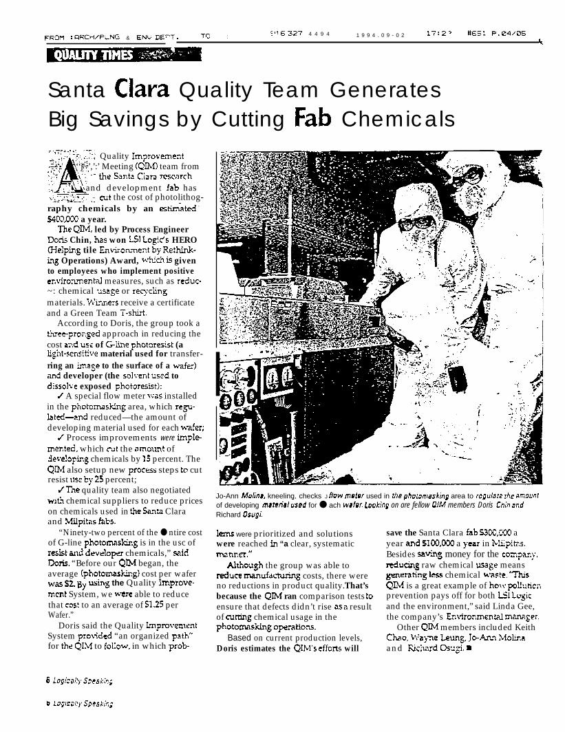
FROM :RRCH/PLNG & ENV DEPT. TO : ~116 327 4 4 9 4 1 9 9 4 . 0 9 - 0 2 17:2~ 8651 P.04/D5
k
Santa Clara Quality Team GeneratesBig Savings by Cutting Fab Chemicals.-..v~.-:.: .-7:.,, .”
,., ,:.. .:l
,AQuality Irnprot”ement... ,’, ;..
?2..:----- ,. ‘‘j~’,’:’ Meeting (QIM) team from::,)+’ V’. - the Santa Clara Kcarch‘~ q. /“ and development fab has,,,,. -:t: ..“-. >4..:—., ,,,: cut the cost of photolithog-raphy chemicals by an esti.m_ated -
!XOO,OOO a year.The QIIvI, led by Process Engineer
Dork Chin, has won M Logids HERO&Ielping tile Entionment by Re&dnk-ing Operations) Award, which is givento employees who implement positiveenvironrnent,al measures, such as reduc-~: chemical usaSe or re~-chngmaterials. W’in.ners receive a certificateand a Green Team T+irt.
According to Doris, the group took athreepronged approach in reducing thecost and us: of Glirre photoresist (aljgljt-scn5itive material used for transfer-ring an imaSe to the surface of a wafer)<and developer (the sol~-ent us~d todissolle exposed photoresist):
/ A special flow meter was installedin the photomasking area, which re=--Iatd-and reduced—the amount ofdeveloping material used for each wafer;
/ Process improvements were implem-ented. which mt the nmount of3eveIopinS chemicals by 15 percent. TheQIM also setup new proc~ss steps to cutresist use by 25 percent;
/ The quality team also negotiatedwiih chemical suppliers to reduce priceson chemicals used in the Santa Claraand Milpitas fabs.
“Ninety-two percent of the ● ntire costof G-line photomas~g is in the usc ofresht and develcIper chemicals,” siiidDC& “Before our QIM began, theaverage (photomasking) cost per waferM,s s2, ~), using the Quality 1mprove-mcnt System, we were able to reducethat Cost to an average of $1.25 perWafer.”
Doris said the Quality Impro~wnentSystem pro~ided “an organized path”for the QI.M to foIIow, in which prob-
Jo-Ann Moiina, kneeling, checks J flow motor used in tile phmomasking area to rcgulaw rhe amounrof developing matetial used for ● ach wafer. Looking on are fellow CUM members Doris Ch;n andRichard ~sugi.
lems were prioritized and solutionswere reached fn “a clear, systematicmi7rmR,”
Aithough the group was able toreduce manufaNuring costs, there wereno reductions in product quality. That’sbecause the QIM ran comparison tests toensure that defects didn’t rise as a resultof aming chemical usage in thephotom,as&g OPeratiOllS.
Based on current production levels,Doris estimates the QI?v[”s effotis will
save the Santa Clara fab S300,00J ayear and 5100,000 a year in N&pitas.Besides savinS money for the coinpar.>,redudng raw chemical usa~e meansgwwrating less chemical w“aste. ‘ThisQIM is a great example of holv pol!uticnprevention pays off for both Ml logicand the environment,” said Linda Gee,the company’s Environmcnal m~amger.
Other QJ2vI members included KeithCbo, Wa]ne Leung, Jo-.%m Molinaand Nclmrd OsJgi. B

FROM :i=RCH/PLNG & ENU DEPT. TO : 916 327 4494 1994, 10-05 09:44 $$795 P.02/02
‘ 4,4
ilyLinda Gc&ewimnmfvmi engineering manager
E nvironment;~l pollution is aconcern to W of us. In our hwsiness,this is an imp{rtant issue since werlccd to use cel-tain typrs of hazard.ous chemicals to manufacture ourhigh-tech products. These chemicalsare considered hazardous due toth[:ir corrosive, flamm:ihlc, reactiveor toxic properties. To minimim ourenvironmental risks, LSI Logic iscommitted to reducing the amount. ofhazardous materials used in ouroperatio~ls and minimizing thenmount of hazardous waste wegenerate.
Our manufacturing sites havedeveloped the following strategies:
d Reduce the amount of hazardousmaterials used through inputchanges, operational improvements,process changes, product reformuk-tions and administrative steps. Twogood examples of chemical reductionefforts occurred recently at theFremont test and assembly facilityand at the Saqt@Clara MD facility.
In Fremont, the use of the toxicchemical chromium—used to removescratches from packaged chips—hasbeen replaced with sodium bicdmn-ate (plain old baking soda). Theresults are even better than the oldmethod, said Engineering SupemisorW-aI1j- Fiecl]er. “Chromium has a
:,—, ,- .,. -— —— ..= —.. ------- . —.. .— . . . . . . . . . . . —-. ..— . . . . . . . . . . . . .-.
LSI Logic Hazardous Waste Disposal, ‘,. “
‘ o 100 “200 %Co 400 “’500 600 7C
TTONS
~F*<>,..,.- : . “ .,-
&J1900” w
Q-. ,. :’ f
b1909 -1.
Iii
\u ,,. ,. .
1 9 9 0 1’.,
“ “al
*.:, ” -,
.; 1991, 9.. :,. .<., , j,.,., . !,..:., , ,.,., .., “1
I
-J,.Environmental Techn;c;an RayMaiden, Ieti and EnvironmentalEngineer Richzrd Bakarpreparedocumenrs for sending o;I to alocal recycipry, Ml rgcycled84percent ofils hmrdous wa.sre12s; ye3r.
?..
;-: , .. . . ,- ,. .

FROM IQRCH/PLNG & ENU DEPT. -rO : 9:6 327 4 4 9 4 1994,C9-02 17:23 8651 P.?5/05
heavy metal content, which is notgood for the environment,” he said.“And since we switched to bakingsoda, the chips look even better. It’sa win-will situation for every one,”
In Santa Clara, the use ofsulfuric aad baths to remove pho-t.oresist from wafers has been re-duced by 60 percent. This wasaccomplished with a three-prongedapproach the frequency of the acidbaths was changed from every fourhours to every eight hours; two wc:tstations for the sulfuric operationwere consolidated to one station; andthe sink reservoir was red~~ed froma two-and. a-half gallon capacity toone-and-a-half gallon capacity. Thenet result: once the six-inch waferconversion ib mmplete, Santa Clarawill use 50 gallon. of sulfuric acidper week. down from ii high of 300gallons a week, according to Photoli-thography Section Manager KeithChao.
W Recj.clc waste materials in thesame process or as a raw material fora different process. An example of
the fomner is at the Milpitas metali.zation fab, where hydrofluoric acid(I-IF) is Used for etctig and cledng
operations, To extend the usefd lifeof H*’ bath solutions, recirculatingfilter systems were installed. By
continuously filtering out paniclecontaminants, the same solutionscan be reused for four or fi~’e processcycles, rather than being d;sposedafter a single cycle, The companj.thus saves on both waste disposalcosts and new chemical purchases.
W Treat waste materials to reducethe voIume of hazard of our wastethat’s generated. h example of thisapproach is utilized at the SantaClara facility, where an on-sitetrearment system has reduced ourtotal HF’ waste volume by 92 percent.As a result of such waste rnhim.izz-tion efforts, the California WalerPollution Control Associationawarded the Santa Clara facility
with a Certificate of .Merit in 19S9.By implementing these three
main techniques, LSI Logic.s U.S.manufacturing sites have been ableto reduce their total volume ofhazardous waste generated by 7Spercent in the past four years.
-, AY
. . .,,... :-:.> :A L :., ,, ...... ”’”.”’ ~..-... .:[email protected],&a/yuafl ha”ds’’~”for~;o? knsirig ~n’stffuric ,acid. -Through process
. . . ---- -“ .,,. . .‘an~”8~ui~rne%:~ruveme~, tie use of the harardo’~ ehetnicalhas beun feducedby60%
t Logicsily Speahng

SILICON SYSTEM SOURCE REDUCTION PROGRAM
2 CASE EXAMPLES
David PaisAugust 26, 1994
As part of our environmental program, Silicon Systems Inc. iscontinually looking for new ways of chemical source reduction andhazardous waste minimization. Source reduction measures includeemployee education, chemical substitutes, and new production methods. Ourmost recent source reduction measures have been the replacement of ourphotoresist stripper and rinse, and plans to reduce photoresist usage.
Photoresist StripperWe have switched positive photoresist strippers to a product with
extended use capabilities. With this new stripper material, we are able to
extend the bath life, and increase the number of wafers per bath. This isexpected to reduce our usage of stripper by 5070. The new rinse will replaceisopropanol (IPA) in the rinse process, reducing usage of IPA by 757o. In
addition to reducing waste, the new rinse is also a safer alternative to ITA by
reducing the fire hazard.
Photoresist ApplicationThe application of photoresist is dependent on the speed at which the
wafer is spinning during application. We are currently testing different timesof application to determine if less chemical could be used on each wafer. Ithas been proposed that by reduang the application time for each wafer, theamount of photoresist applied could be reduced by almost 5070 without
sacrificing product quafity.
Production demands in the semiconductor industry make sourcereduction an exhemely challenging task. Every major process changerequires engineering qualification to ensure product quality and reliability are
maintained. By exploring new chemicals and processes, SSi has been able to
significantly reduce generation of hazardous waste, and hopes to continue
this trend in the future.
81
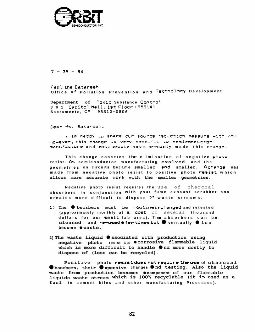
7 - 29 - 94
Paul ine BatarsehO f f i c e uf P o l l u t i o n P r e v e n t i o n a n d Technology D e v e l o p m e n t
Department of Taxic Substance Control3 0 1 Cauitol Mall, Lst FIoor (95e14)Sacramento, CA 95S12-0806
: ~m nacoy :~ snare cur sour~~ -scuc:icn measure -41:- ~cu.
ticwever, t h i s change i= very =ceci:i= co Semicanauc:or,manufacture a n d most Decole n a v e >r=oaDIy m a d e t h i s cnanqe.
T h i s c h a n g e c o n c e r n s the e l i m i n a t i o n o f n e g a t i v e ghoccresist . As semiconducto r manu fac tu r i ng evolved a n d t h eg e o m e t r i e s on circuits became smaller and smaller. A cnange wasm a d e f r o m n e g a t i v e p h o t o r e s i s t t o p o s i t i v e p h o t o resist w h i c hallows more accurate work with the smaller geometries.
Negative photo resist requires the use of charcoala b s o r b e r s i n c o n j u n c t i o n wi th you r f ume exhaus t sc rubbe r ana
c r e a t e s m o r e d i f f i c u l t t o d i s p o s e =f w a s t e s t r e a m s .
1) The ● bsorbers must be routinely changed and retested(approximately monthly at a cost of several t h o u s a n dd o l l a r s f o r o u r small f a b a r e a ) . The a b s o r b e r s c a n b ecleaned and re-used ● few times but ● ventually ● l s obecome ● waste.
2) The waste liquid ● ssociated with production usingnegative photo resist is ● corrosive flammable liquidwhich is more difficult to handle ● nd more costly todispose of (less can be recycled).
Positive photo resist do- not rewir= the use of charcoal● bsorbers, their ● xpensive changes ● nd testing. Also the liquidwaste from production becomes ● component of our flammableliquids waste stream which is 100Z recyclable (it is used as afuel i n cement k i l ns and o the r manu fac tu r i ng P rocesses ) .
82

mlSEMICONWOQ- NC
Changing to positive photo resist was somewhat costly, butwill continue paying for itself.
I hope this information is useful to you. Any questionsplease give me a call.
\
Ch_-Ies Wurm (408) 744-1S00 x230Environmental / Safety Officer fax (400) 744-0249
C?rbit Semiconductor, Inc.1215 Bordeaux DriveS~nyvale, CQ9 940e9

SOURCE REDUCTION =ASURE ATAliAIA)G DBVTCBS
Atid co ntaminated soiid waste reducti~In Octiber, 1993, we began to educate employees on how to reduce acidcent.amu.n- ated waste. We used a 7-Step Total Quality Management (TQM)process to isolate the problems and identi& weaknesses. A number of actionitems were implemented such as additional training, trash can signs, pHpaper stitions, glove washing procedures, and the purchase of an acid spillvacuum Operators were asked to report equipment problems and leaks.Un.knovm spills were checked with pH paper to ensure that a spill washazardous and not just water. A vacuum was purchased to take care of largerliquid SpillS. T& would minimize the use of wipes for cIean-up. pH paperstations were inst.ded throughout the fab so that acid gloves could be rinsedand checked for acid residue prior to disposal to non-hazamlous trash.
These changes have reduced our acid contiated solid wastx streamconsiderably. Below is a comparison of acid contarninated solid waste totalsfor the first 7 months of each year be=ginn.ingin 1992.
Janu=-Y - JUIY. ISSZ 11,600 pounds.JanU=Y - Jdy. 1993 10,700 pounds I’8Tc retiu~tion from 3?2)January - July, 1994 ,j,200 Dounds 5i5% reauction tom L9f?2).
We also made employees more aware of the Werent waste cans availabie byplacing additional signs on disposal cans. ‘~-e conduc-~d spot checks ofhazardous waste cans to look for non-hazardous waste. In the beginning asmuch as 159’c of hazardous waste in these cans was actually non-hazardous.
Other ActivitiezIn addition to the SB-14 waste reduction plan. we have eliminated the use ofCFC’S and Glycol ethers in our production processes. We aiso changed ourAcid Neutralization system. Instead of So&urn hycirofide, we use Magnesiumhydrofide and sulfuric acid to neumtize ‘he wasw acids and bases.
84
ODC ELIMINATION PROJECT
Ozone Depleting Chemicals (ODC) are commonly used in the electronics industry as adrying agent in the final step of a wet process for electronic componentsmanufacturing. Examples of the wet process can be the plating of a metal, such asnickel or gold, the etching of a metal by acids for cleaning or surface roughening, orthe final cleaning of a component prior to packaging to the customer. In themanufacture of ceramic pin grid arrays (PGAs), Alcoa Electronic Packaging, Inc. useda specific chemical of the family of ODCS or chlorofluorocarbons (CFCS) called Freon-113 as a drying agent in three areas: after the first nickel plating operation, after thesecond nickel and gold plating operation and in the final cleaning of finished pansprior to packing for shipment to the customer.
Freon acts as a drying agent by displacing the water that remains on a part after thefinal rinsing of the chemical process. The Freon simply floats the rinse water from thesurface of the part, and since Freon does not mix with water, the rinse water iscollected from the Freon bath and removed. The rinse water, which generally containssmall” amounts of contaminants, such as dissolved plating salts, organics and otherwater soluble contaminants, is thus removed from the part. The stains will render thepart rejectable as per the customer specification.
Alcoa Electronic Packaging, Inc. started in November of 1990 to develop an alternativeFreon-free drying process for the first nickel plating line. A task force was assembledto evaluate the cause of the high level of stains, 35 percent, at this operation. Initialanalysis of the stained areas of the PGAs showed the stain to be composed ofinorganic residue. Following this analysis, an experiment was performed to test theuse of an ultra clean hot water rinse (monitored by a resistivity meter) and then hot airdry. The initial test results showed the level of stains using this method produced asignificant improvement over the Freon cleaning method. After repeating thisexperiment several more times with similar results, it was decided in January of 1991to eliminate the Freon dryer from the first nickel plating operation. This was our firstdemonstration that hot, uttra clean deionized (Dl) water controlled by a resistivity metercould replace Freon.
By mid 1991 the level of stains had stabilized at 17 percent, and the only Freon usedin production was used at the drying process at final nickeVgold where the hot DImethod had not yet been perfected for the more sensitive gold plated pans. At thesame time, the level of stains at the final clean operation where the hot DI method wasbeing used was climbing at a steady rate along with production volume. In Septemberof 1991, Freon cleaning was successfully installed at this final cleaning operationreducing the final clean stain level to 3.8 percent. By mid 1992 the level of Freonemissions had reached an all time high of about 90 pounds per day, and the cost ofFreon had peaked at $24,000 per month. Wtihout Freon elimination at the first nickeloperation, the cost would have “been 60°A higher.
Several factors, including the facilities upgrade of the incoming deionized watersystem, the improved density of the packages being produced and a more efficientlogistics system of getting patis from semnd nickel/gold to the final clean operation,

enabled us in May of 1992 to eliminate Freon as the drying process on the secondnickel/gold line, significantly reducing ODC emissions and realizing a cost savings inFreon expense.
With the success of the second nickel/gold Freon elimination and successful progressin the hot DI water/air dry method of parts drying, Freon was replaced in the electrolessnickel line in June of 1992 with the hot Di water/air dry system. This fuflher reducedthe ODC emissions level from 60 pounds per day to 37 pounds.
The greatest challenge remaining was the elimination of Freon at the most criticalcleaning operation, final clean, the operation just prior to packing the PGAs forcustomer shipment. Alcoa Electronic Packaging, Inc.’s scientists and engineersaggressively and successfully expedited the development of the hot DI water/hot drdry cleaning method for that application surpassing the cleaning capability of theFreon method. Thus the final clean Freon process was eliminated reducing CFC plantemissions levels to zero.
Today, the non-Freon, hot DI water/hot air drying method produces PGAs with a stainlevel of less than 1 percent. If Freon had not been eliminated from the cleaning stepsat the operations where it was removed, given the present production level, and thefact that the cost of Freon has tripled from $3.50 /lb. in 1992 to $9.98/lb today, the costof Freon would be $1 ,074,800/ month, which equates to an annualized savings of$12,900,000.
Environmentally the impact is equally impressive. In eliminating Freon from allprocesses where it had existed (based on current production rate), potentially 440,000pounds per year of CFC emissions has been eliminated by Alcoa ElectronicPackaging, Inc.