at78c1503 dvd/cd read channelebook.pldworld.com/_semiconductors/atmel/databook cdrom... ·...
TRANSCRIPT
DVD/CD Read Channel
AT78C1503
Rev. 1214C–03/00
Features• Operating Supply Range 3.0V to 3.6V• Power Dissipation 1W Max• Low-power Sleep Mode (<0.5 mW)• RF Data Channel
– Automatic Gain Control or Programmable Gain Mode– Wide Bandwidth VGA– VGA Accepts Inputs from 30 - 300 mV Peak-to-Peak Differential (PPD),
60 - 600 mVPPD or 110 - 1100 mVPPD– Programmable Equalization via 7th-order Equiripple Filter with Programmable
Symmetric Zeros– Programmable 5-to-1 Filter Cutoff Range– Data Slicer with DC Restore Circuit– Wide Frequency Range Clock Extraction– Frequency Synthesizer with Independent 7-bit M and 6-bit N Dividers,
Better than 1% Resolution– Highly Programmable to Accommodate DVD (1 - 5X) and CD (6 - 30X)– Write Asymmetry Measurement for Adjusting Write Mode Power– Data Recovery Supports CLV, ZCLV, ZCAV Recording– Optional Internally Generated Timing for AGC and Timing Recovery
• Servo Algebra Functions– 45 MHz Bandwidth for Differential Phase Tracking Detector– Land and Groove Detector for DVD RAM– Supports One Beam Push-pull Tracking Output– Supports One Beam Differential Phase Tracking– Focus Error Signal Output– Focus OK Signal– Track Crossing Detection– Mirror Signal Output– Wobble Detection for DVD RAM, DVD+RW– Header Detection for DVD RAM
Description
The AT78C1503 is a programmable DVD/CD channel responsible for servo algebra,gain control, equalization, bit detection and clock extraction for CD-ROM, DVD-ROM,DVD+RW and DVD-RAM data. Programmable features allow data rates up to 5XDVD. Also for DVD-RAM functionality, the channel serves the write path providing 1Xwrite clock (WCLK) and pit asymmetry detection. The CMOS channel operates from asingle 3.3V supply and is fully programmable through a serial interface for both CDand DVD modes.
1

Figure 1. AT78C1503 Block Diagram
SYNTHESIZERFREQUENCY
MUX
FOCUS OK
SERIALREGISTER
TP1 TP2
RFP/N
RG
WGPD
MODECONTROL
SlowArithmetic and
Push-pull
Focus Error
MirrorDetector
Normalization
Tracking
SENA SCLK SDAT
MIRROR
RDSZ
REXT
2
TRK
FE
ID12
FOK
TETZC
WBL
ID34
WobbleDetectorLand GrooveDetector SLOWSUM
Sum orDifference
(IDSEL)
SERREG
CAGC
Control(RF Sequencer)
AGCControlVoltage
Loop Cap
fcdac/range boostdac
RFDRPFO2_CDFO1_CD
TR2_CDTR1_CD
2
2
2
2
2
2RFGEN
F
HG
E
DATA5DATA4
RCLK
FREF
DATA6DATA7
DATA1DATA0
DATA2DATA3
DATAPLL
AGCControl
D/SE
127
TEST
VREF
D/SED/SE
D/SE1
11
1
AGCLZAGCFSTAGCHLD
IDSEL
AP/N
BP/N
CP/N
DP/N
PGC
PGC
PGC
PGC
MUX VGA7th OrderFilter/Equalizer
DifferentialTrackingDetector
AutoInv
TRACK OKTRACK ZERO
CROSS
MUX
DCRestore
8.5X+
-
Σ
Σ
AT78C15032
AT78C1503
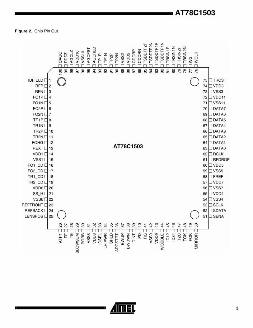
Figure 2. Chip Pin Out
IDFIELDRFPRFN
FO1PFO1NFO2PFO2NTR1PTR1NTR2PTR2N
FOHGREXTVDD1VSS1
FO1_CDFO2_CDTR1_CDTR2_CD
VDD6SS_HVSS6
REFFRONTREFBACKLENSPOS
TRCSTVDD3VSS3VDD11VSS11DATA7DATA6DATA5DATA4DATA3DATA2DATA1DATA0RCLKRFDROPVDD5VSS5FREFVDD7VSS7VDD4VSS4SCLKSDATASENA
AT
P1
FE
TE
SLO
WS
UM
PO
RB
VS
S8
VD
D8
IDS
EL
LHIP
WR
SH
LDA
DC
ST
RT
BW
UP
BW
DW
NID
INT
PD
RG
VS
S9
VD
D9
WO
BB
LEID
12ID
34T
ZC
TO
KF
OK
MIR
RO
R
CA
GC
RD
SZ
AG
CLZ
VD
D10
VS
S10
AG
CF
ST
AG
CH
LDT
P1P
TP
1NT
P2P
TP
2NV
SS
2V
DD
2C
DC
RP
CD
CR
NT
SD
DT
P2P
TS
DD
TP
2NT
SD
DT
P1P
TS
DD
TP
1NT
RS
IN1P
TR
SIN
1NT
RS
IN2P
TR
SIN
2NW
GW
CLK
AT78C1503
12345678910111213141516171819202122232425
75747372717069686766656463626160595857565554535251
100 99 98 97 96 95 94 93 92 91 90 89 88 87 86 85 84 83 82 81 80 79 78 77 76
26 27 28 29 30 31 32 33 34 35 36 37 38 39 40 41 42 43 44 45 46 47 48 49 50
3
Functional DescriptionThe AT78C1503 is a programmable DVD/CD channelresponsible for servo algebra, gain control, equalization, bitdetection and clock extraction for CD-ROM, DVD-ROM,DVD+RW and DVD-RAM data. Programmable featuresallow data rates up to 5X DVD. Also for DVD-RAM func-tionality, the channel serves the write path providing laserpower control and pit asymmetry detection. The CMOSchannel operates from a single 3.3V supply and is fully pro-grammable through a serial interface for both CD and DVDmodes. The IC contains two separate processing channels.One for RF signal detection and synchronization, and theother for focus and tracking servo control. These arereferred to as the RF channel and the servo channelrespectively
RF Channel Overall DescriptionThe RF channel consists of gain control, equalization, bitdetection and clock extraction and is shown in the blockdiagram of Figure 1. The readback signal is internally ACcoupled from the preamplif ier to the channel inputRFP/RFN. A variable gain amplifier (VGA) is used for gaincontrol of the readback signal. A 7th order equiripple fil-ter/equalizer is used for noise filtering and equalization ofthe signal before detection. The output of the equalizerfeeds a fixed gain of 8.5 bringing the internal level up toapproximately 750 mV peak-to-peak differential (mVppd).The output of the 8.5X amplifier enters the AGC controlblock which closes the AGC loop to maintain a 750 mVppdslicer input level while RF P/N is allowed to vary ten to one.The data slicer has a programmable slicing level or anadaptive DC restore system to maintain a DC free output ofthe slicer. The data slicer output is a digital stream and issent to the clock extraction and synchronization circuitry.Clock extraction is performed with the data PLL which isoperated in phase/frequency mode during write and idlemodes and phase only mode when reading data. An onboard frequency synthesizer is used for locking the dataPLL to a close initial frequency upon start up. Various testoutputs are provided to aid the evaluation of the system. Inaddition an offset calibration routine executed on power upeliminates the need for internal AC coupling by correctinginternal offsets over the parts operating conditions.
Gain Control
The front-end gain control on the AT78C1503 consists offive differential Variable Gain Amplifiers (VGAs). Theyinclude a VGA for the RF path and four ProgrammableGain Control (PGC) amplifiers for A, B, C and D inputs. The
voltage gain range for the VGAs can be programmed bysetting the VGAMODE<1:0> control bits (see Figure 3).There are two primary modes of operation for the RF path:Automatic Gain Control (AGC) mode and ProgrammableGain Control (PGC) mode.
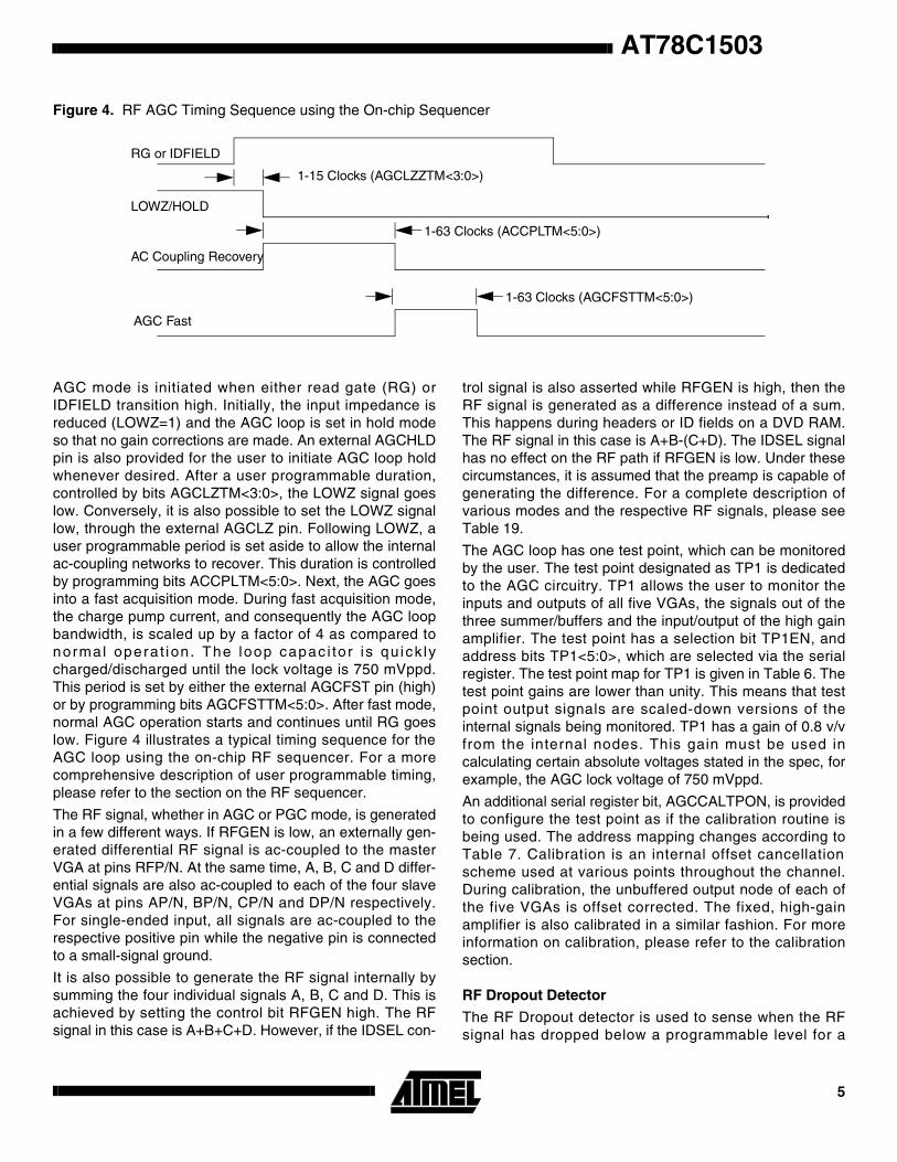
In AGC mode (PGCEN=0), the master VGA is part of theAGC loop. The loop a lso conta ins the 7th orderfilter/equalizer, a fixed high-gain stage, an amplitudedetector, a dual rate charge-pump, an internal loopfilter/capacitor and an exponentiator (see Figure 3). TheVGA voltage gain is adjusted by the feedback control loopsuch that the signal at the input of the amplitude detector isabout 750 mVppd. Gain tracking is achieved by applyingthe same gain control signals to the four slave VGAs.
Figure 3. AGC Loop Block Diagram
In PGC mode (PGCEN=1), the master VGA gain is setdirectly by programming the PGC DAC through the serialinterface (see Table 5). Once again, gain control signalsare shared between the master and the four slave VGAs.
The AGC loop is of the peak sampling type in whichasymmetric charge/discharge currents are used. Thesecurrents are programmable through bits AGCQP<3:0> (seeTable 4). They are derived from the internal bandgapvoltage reference and the external resistor REXT, resultingin a near zero temperature coefficient. The absolute valueis process dependent varying with the internal bandgapvoltage (±5%) as well as due to tolerance of the externalresistor. The charge current continuously charges up theAGC capacitor. A 16X discharge current results for theduration the signal is above the 100% threshold (i.e. 750mVppd). The large discharge/charge ratio causes the loopto adjust the VGA gain based on the peak amplitude of thesignal. As a result, the peaks of the signal are locked to aknown voltage (i.e. 750 mVppd).
RF in VGAFILTER
EQUALIZER8.5X
QPUMP AMPLITUDEDETECTOR
EXP
CAGC350pF
ToDetector
internal
AT78C15034
AT78C1503
Figure 4. RF AGC Timing Sequence using the On-chip Sequencer
AGC mode is initiated when either read gate (RG) orIDFIELD transition high. Initially, the input impedance isreduced (LOWZ=1) and the AGC loop is set in hold modeso that no gain corrections are made. An external AGCHLDpin is also provided for the user to initiate AGC loop holdwhenever desired. After a user programmable duration,controlled by bits AGCLZTM<3:0>, the LOWZ signal goeslow. Conversely, it is also possible to set the LOWZ signallow, through the external AGCLZ pin. Following LOWZ, auser programmable period is set aside to allow the internalac-coupling networks to recover. This duration is controlledby programming bits ACCPLTM<5:0>. Next, the AGC goesinto a fast acquisition mode. During fast acquisition mode,the charge pump current, and consequently the AGC loopbandwidth, is scaled up by a factor of 4 as compared tonormal opera t ion . The loop capac i to r i s qu ick lycharged/discharged until the lock voltage is 750 mVppd.This period is set by either the external AGCFST pin (high)or by programming bits AGCFSTTM<5:0>. After fast mode,normal AGC operation starts and continues until RG goeslow. Figure 4 illustrates a typical timing sequence for theAGC loop using the on-chip RF sequencer. For a morecomprehensive description of user programmable timing,please refer to the section on the RF sequencer.
The RF signal, whether in AGC or PGC mode, is generatedin a few different ways. If RFGEN is low, an externally gen-erated differential RF signal is ac-coupled to the masterVGA at pins RFP/N. At the same time, A, B, C and D differ-ential signals are also ac-coupled to each of the four slaveVGAs at pins AP/N, BP/N, CP/N and DP/N respectively.For single-ended input, all signals are ac-coupled to therespective positive pin while the negative pin is connectedto a small-signal ground.
It is also possible to generate the RF signal internally bysumming the four individual signals A, B, C and D. This isachieved by setting the control bit RFGEN high. The RFsignal in this case is A+B+C+D. However, if the IDSEL con-
trol signal is also asserted while RFGEN is high, then theRF signal is generated as a difference instead of a sum.This happens during headers or ID fields on a DVD RAM.The RF signal in this case is A+B-(C+D). The IDSEL signalhas no effect on the RF path if RFGEN is low. Under thesecircumstances, it is assumed that the preamp is capable ofgenerating the difference. For a complete description ofvarious modes and the respective RF signals, please seeTable 19.
The AGC loop has one test point, which can be monitoredby the user. The test point designated as TP1 is dedicatedto the AGC circuitry. TP1 allows the user to monitor theinputs and outputs of all five VGAs, the signals out of thethree summer/buffers and the input/output of the high gainamplifier. The test point has a selection bit TP1EN, andaddress bits TP1<5:0>, which are selected via the serialregister. The test point map for TP1 is given in Table 6. Thetest point gains are lower than unity. This means that testpoint output signals are scaled-down versions of theinternal signals being monitored. TP1 has a gain of 0.8 v/vfrom the internal nodes. This gain must be used incalculating certain absolute voltages stated in the spec, forexample, the AGC lock voltage of 750 mVppd.
An additional serial register bit, AGCCALTPON, is providedto configure the test point as if the calibration routine isbeing used. The address mapping changes according toTable 7. Calibration is an internal offset cancellationscheme used at various points throughout the channel.During calibration, the unbuffered output node of each ofthe five VGAs is offset corrected. The fixed, high-gainamplifier is also calibrated in a similar fashion. For moreinformation on calibration, please refer to the calibrationsection.
RF Dropout Detector
The RF Dropout detector is used to sense when the RFsignal has dropped below a programmable level for a
RG or IDFIELD
LOWZ/HOLD
1-15 Clocks (AGCLZZTM<3:0>)
AC Coupling Recovery
1-63 Clocks (ACCPLTM<5:0>)
1-63 Clocks (AGCFSTTM<5:0>)
AGC Fast
5

specified amount of time. The RF dropout detector gets itsinput from the 8.5 V/V gain stage immediately before theDC restore block. There is a programmable windowdetector which the RF signal passes through. The absoluteva lue o f t h i s w indow has the fo l l ow ing va lue :(RFDTH<4:0>+1)*3.5 mV+115 mV. The result of thiscomparison is captured by comparators clocked at thesynthesizer clock rate divided by two. The output of thewindow comparator enters a counter in which the durationof the assertion of the window detector is monitored. If thewindow detector output remains asserted, longer thanRFDROPCNT<4:0> system clocks, the RFDROP pin willbe asserted. The assertion of the window detectorindicates the RF signal is below the programmed value.The RF dropout detector clock is the synthesizer ratedivided by two.
Once the signal has been restored in amplitude, theRFDROP pin will be deasserted. There is no attempt tomake use of this signal internal to the channel.
In order for the RF dropout to operate the RFDROPEN bitmust be programmed high. When this bit is low, thedropout detector will be powered down.
7th-order Filter/Equalizer
The on board filter/equalizer is implemented as a 7 pole 2symmetric zero 0.05 degree equiripple phase low-passfilter. Cutoff frequency for the filter spans 4 - 26 MHz in 6coarse steps, set by serial register 9, FLTRRANGE<2:0>,with fine control within each coarse step controlled by a 6-bit dac; FCDAC<4:0>. Two programmable zeros provideuser controlled boost up to 14dB from the low frequencygain. The two zeros may be set to track one another,ASYMBST=0, to provide flat group delay independent ofboost or the zeros can be programmed independentlythereby providing group delay adjustment, ASYMBST=1. Inthe case of symmetric boost, BST1<3:0> controls theamount of boost; see Table 30. For asymmetric zeros,BST1<3:0> and BST2<3:0> independently control the twozeros. Group delay variation is maintained within ±4% outto 1.5 times the cutoff frequency when ASYMBST=0.
Individual Q adjust is also provided for the three biquadswhich make up the filter. These Qs can be independentlyadjusted if a slightly different transfer function other thanthe equiripple is desired. The amount of Q adjust isdetermined by serial registers BQD1-3Q<3:0>, see Table31.
When boost greater than 7 dB above the DC level isrequired, the gain through the filter needs to be reduced inorder to reduce the amount of signal distortion originatingfrom the filter. The bit FLTRGAIN should, therefore, be set
high when more than 7dB of gain is required, this willreduce the signal amplitude through the filter by a factor oftwo.
The filter cutoff is stabilized over supply and temperaturevariations by using an external resistor and an internal con-trol loop. Absolute cutoff is guaranteed within ±10% of thespecified value. The filter is incorporated into the AGC loopalong with a final gain of 8.5 V/V amplifier to bring the finaldetector input up to 750 mVppd. The signals at every pointthroughout the Continuous Time Filter (CTF) are availablevia TP2 for testing and system evaluation, see Table 8.
RF Data Detector and DC Restore
The output of the high gain amplifier inside the AGC loop isthe input to the RF detector. The detector can be operatedin three distinct modes controlled by bits DETMODE<1:0>(see Table 10). These modes are DC-restore mode, Com-parator mode and Write Power Test mode.
During normal operation (DC-restore mode), the detector isa slicer with the slicing threshold set automatically by aninternal feed back loop. This is depicted in Figure 4.
Figure 5. Data Slicer with DC Restore
The loop consists of a charge pump and an external inte-grating capacitor. The digital output of the slicer isintegrated and subtracted from the input removing anybaseline variation. The charge pump current is programma-ble and can be set through bits DETCPI<1:0> andDETKCP<1:0> in the serial register. In comparator mode,the feedback loop is disabled and the slicing threshold isset manually by programming a DETTHRSH. Lastly, inWrite Power Test mode, the detector is used in asymmetrydetection for determining written pit asymmetry. In thismode the feedback loop is disabled, the loop filter/capacitoris reset to zero and the digital output of the slicer is inte-grated. The resulting voltage is then used to adjust thewrite power to be within some desirable range.
A number of detector internal signals can be monitored attest point TSDD1<3:0> (see Table 14). These include, thevoltage on the loop filter/capacitor, the input to the slicerinput, and the digital output of the slicer.
SLICER DetectorOutput
Vth
0 VthDAC
CQPUMP
EQData
-+2
2
2
AT78C15036
AT78C1503
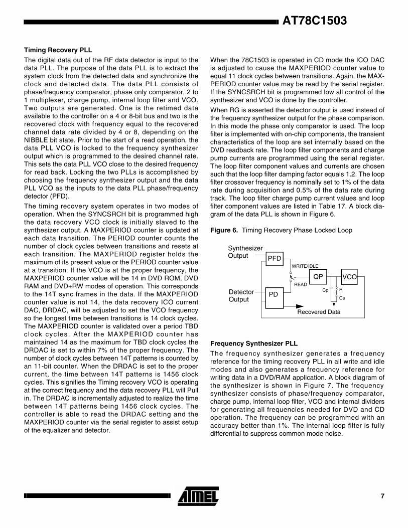
Timing Recovery PLL
The digital data out of the RF data detector is input to thedata PLL. The purpose of the data PLL is to extract thesystem clock from the detected data and synchronize theclock and detected data. The data PLL consists ofphase/frequency comparator, phase only comparator, 2 to1 multiplexer, charge pump, internal loop filter and VCO.Two outputs are generated. One is the retimed dataavailable to the controller on a 4 or 8-bit bus and two is therecovered clock with frequency equal to the recoveredchannel data rate divided by 4 or 8, depending on theNIBBLE bit state. Prior to the start of a read operation, thedata PLL VCO is locked to the frequency synthesizeroutput which is programmed to the desired channel rate.This sets the data PLL VCO close to the desired frequencyfor read back. Locking the two PLLs is accomplished bychoosing the frequency synthesizer output and the dataPLL VCO as the inputs to the data PLL phase/frequencydetector (PFD).
The timing recovery system operates in two modes ofoperation. When the SYNCSRCH bit is programmed highthe data recovery VCO clock is initially slaved to thesynthesizer output. A MAXPERIOD counter is updated ateach data transition. The PERIOD counter counts thenumber of clock cycles between transitions and resets ateach transition. The MAXPERIOD register holds themaximum of its present value or the PERIOD counter valueat a transition. If the VCO is at the proper frequency, theMAXPERIOD counter value will be 14 in DVD ROM, DVDRAM and DVD+RW modes of operation. This correspondsto the 14T sync frames in the data. If the MAXPERIODcounter value is not 14, the data recovery ICO currentDAC, DRDAC, will be adjusted to set the VCO frequencyso the longest time between transitions is 14 clock cycles.The MAXPERIOD counter is validated over a period TBDclock cyc les . Af ter the MAXPERIOD counter hasmaintained 14 as the maximum for TBD clock cycles theDRDAC is set to within 7% of the proper frequency. Thenumber of clock cycles between 14T patterns is counted byan 11-bit counter. When the DRDAC is set to the propercurrent, the time between 14T patterns is 1456 clockcycles. This signifies the Timing recovery VCO is operatingat the correct frequency and the data recovery PLL will Pullin. The DRDAC is incrementally adjusted to realize the timebetween 14T patterns being 1456 clock cycles. Thecontroller is able to read the DRDAC setting and theMAXPERIOD counter via the serial register to assist setupof the equalizer and detector.
When the 78C1503 is operated in CD mode the ICO DACis adjusted to cause the MAXPERIOD counter value toequal 11 clock cycles between transitions. Again, the MAX-PERIOD counter value may be read by the serial register.If the SYNCSRCH bit is programmed low all control of thesynthesizer and VCO is done by the controller.
When RG is asserted the detector output is used instead ofthe frequency synthesizer output for the phase comparison.In this mode the phase only comparator is used. The loopfilter is implemented with on-chip components, the transientcharacteristics of the loop are set internally based on theDVD readback rate. The loop filter components and chargepump currents are programmed using the serial register.The loop filter component values and currents are chosensuch that the loop filter damping factor equals 1.2. The loopfilter crossover frequency is nominally set to 1% of the datarate during acquisition and 0.5% of the data rate duringtrack. The loop filter charge pump current values and loopfilter component values are listed in Table 17. A block dia-gram of the data PLL is shown in Figure 6.
Figure 6. Timing Recovery Phase Locked Loop
Frequency Synthesizer PLL
The frequency synthesizer generates a frequencyreference for the timing recovery PLL in all write and idlemodes and also generates a frequency reference forwriting data in a DVD/RAM application. A block diagram ofthe synthesizer is shown in Figure 7. The frequencysynthesizer consists of phase/frequency comparator,charge pump, internal loop filter, VCO and internal dividersfor generating all frequencies needed for DVD and CDoperation. The frequency can be programmed with anaccuracy better than 1%. The internal loop filter is fullydifferential to suppress common mode noise.
PFD
SynthesizerOutput
QP VCO
PDDetectorOutput
WRITE/IDLE
READ
Recovered Data
Cp
Cs
R
7
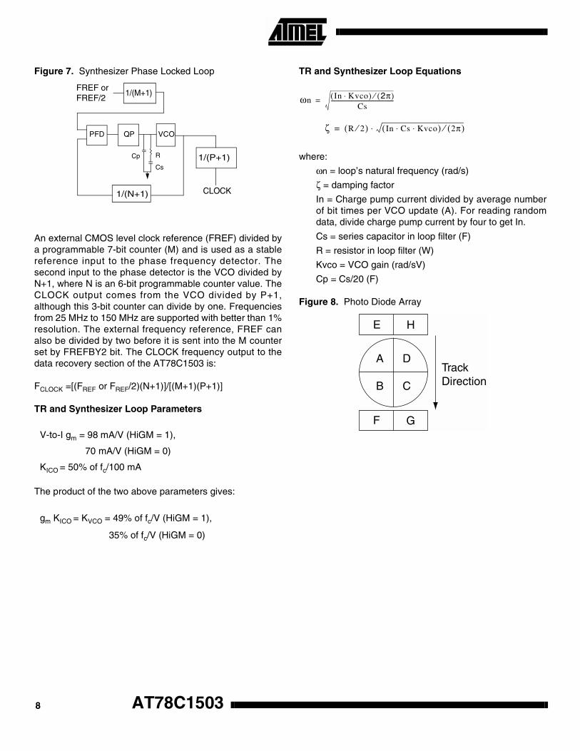
Figure 7. Synthesizer Phase Locked Loop
An external CMOS level clock reference (FREF) divided bya programmable 7-bit counter (M) and is used as a stablereference input to the phase frequency detector. Thesecond input to the phase detector is the VCO divided byN+1, where N is an 6-bit programmable counter value. TheCLOCK output comes from the VCO divided by P+1,although this 3-bit counter can divide by one. Frequenciesfrom 25 MHz to 150 MHz are supported with better than 1%resolution. The external frequency reference, FREF canalso be divided by two before it is sent into the M counterset by FREFBY2 bit. The CLOCK frequency output to thedata recovery section of the AT78C1503 is:
FCLOCK =[(FREF or FREF/2)(N+1)]/[(M+1)(P+1)]
TR and Synthesizer Loop Parameters
The product of the two above parameters gives:
TR and Synthesizer Loop Equations
where:
ωn = loop’s natural frequency (rad/s)
ζ = damping factor
In = Charge pump current divided by average numberof bit times per VCO update (A). For reading randomdata, divide charge pump current by four to get In.
Cs = series capacitor in loop filter (F)
R = resistor in loop filter (W)
Kvco = VCO gain (rad/sV)
Cp = Cs/20 (F)
Figure 8. Photo Diode Array
V-to-I gm = 98 mA/V (HiGM = 1),
70 mA/V (HiGM = 0)
KICO = 50% of fc/100 mA
gm KICO = KVCO = 49% of fc/V (HiGM = 1),
35% of fc/V (HiGM = 0)
PFD QP VCO
1/(N+1) CLOCK
1/(M+1)FREF or
Cp
Cs
R 1/(P+1)
FREF/2 ωn In Kvco⋅( ) 2π( )⁄Cs
--------------------------------------------=
ζ R 2⁄( ) In Cs Kvco⋅ ⋅( ) 2π( )⁄⋅=
A D
B C
F G
E H
TrackDirection
AT78C15038

AT78C1503
Figure 9. Fast Servo Arithmetic
Servo Channel Description
The AT78C1503 servo channel can process data from twotypes of photodiode arrays. The most common type is theA,B,C,D only array. The other type of array is an 8 elementarray (see Figure 8) in which Differential Push Pull trackingor Push Pull tracking may be used. As shown in Figure 1,there are 4 differential signals: AP/N, BP/N, CP/N, DP/N.These inputs can also be used in a single ended fashion bynot connecting the negative side and also setting bit TBD inthe serial register to indicate that a single ended interfacehas been selected. In addition to the differential A, B, C andD input signals the outputs of the E, F, G and H photodiodes are connected as single ended input signals to the78C1503 to be used in the Differential Push-Pull trackingalgebra.
Servo algebra is performed for focus, push-pull tracking,differential phase tracking, tangential push pull andland/groove detection. The input signals on the A, B, C andD pins are used to internally generate the astigmatic focusand tracking error signals. Additionally the input pins E, F,G and H may be used to internally generate the differentialpush-pull tracking signal.
A block diagram of the fast servo arithmetic functions areshown in Figure 9 and a block diagram of the slow servoarithmetic functions are shown in Figure 11.
Fast Servo Arithmetic Functions
Differential Phase Tracking
The Differential Phase Tracking block diagram shown inFigure 9 generates the servo tracking error for DVD ROM.Differential inputs A, B, C and D, are AC-coupled using on-chip capacitors. The AC-coupling pole is nominally set to 6kHz. Each of these differential signals then goes through aProgrammable Gain Control (PGC) set up via the serialregister. The PGCs are followed by adjustable delays
nominally set to TBD ns. The delays on the signals from thefront of the detector, A and D, are adjusted to an amount αthat is greater than the nominal delay, whereas the delayson signals from B and C signals are adjusted to α,=less thanthe nominal delay. The delayed signals are followed by twohigh-speed summers to generate the diagonal sums A+C &B+D. The output signals of the summers is delayed by adifferent nominal value plus and minus an adjustableamount, β.=That is, the output A+C is delayed by a nominalamount plus an adjustable amount, β,=and the output B+Dis delayed by the same nominal value minus β.Theadjustable delays are realized with second-order all passBessel filters.
The signal level coming out of the second set of delays istypically between 100-150 mVppd. Each of the twodiagonal sums is buffered, amplified and equalized. Theequalizer transfer function is depicted in Figure 10 andincludes a zero followed by two poles. The zero and thetwo poles track the DVD setting according to Table 20.
Equalized diagonal sums (A+C & B+D) are sliced around afixed threshold and phase compared to generate pump-upand pump-down pulses. The phase comparator output isautomatically disabled when no transitions are detected oneither one of its two inputs.
Following the phase comparator is a low-pass filter whichintegrates the pump-up and pump-down pulses to generatethe differential phase tracking error signal. The low-passfilter consists of a charge-pump and on-chip integratingcapacitors. The pole frequency is programmable from 30kHz to about 2.5 MHz. When DPDDIVSEL is high, the polefrequency can be set directly through bits DPDDIVhi<3:0>(see Table 23). When DPDDIVSEL is low, however, thelow-pass cutoff frequency is adjusted automatically by anup/down counter. This feature allows the low-pass filterbandwidth to track seek speeds during seek mode. A user-
2
2
2
2
B+D
A+CLPF
2
2
LPF
QP
CP/N
DP/N
AP/N
BP/N
VGA
VGA
VGA
VGA
VGA
VGA
EQ
EQ
PD TE
2
2
DPDKPGC<3:0>4
DPDVGABYP DPDLPFBYP
From serial register
Differential to single-endedconverter plus VGA
UP
DN
DPDKSEVGA<3:0>
4
DEL
DEL
DEL
DEL
DEL1
DEL1
9
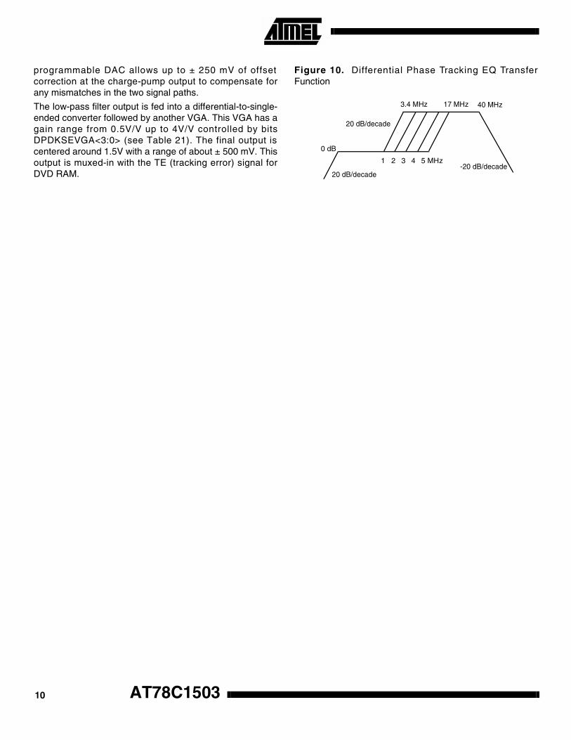
programmable DAC allows up to ± 250 mV of offsetcorrection at the charge-pump output to compensate forany mismatches in the two signal paths.
The low-pass filter output is fed into a differential-to-single-ended converter followed by another VGA. This VGA has again range from 0.5V/V up to 4V/V controlled by bitsDPDKSEVGA<3:0> (see Table 21). The final output iscentered around 1.5V with a range of about ± 500 mV. Thisoutput is muxed-in with the TE (tracking error) signal forDVD RAM.
Figure 10. Differential Phase Tracking EQ TransferFunction
20 dB/decade
-20 dB/decade20 dB/decade
1 2 3 4 5 MHz
3.4 MHz 17 MHz 40 MHz
0 dB
AT78C150310
AT78C1503
Slow Servo Arithmetic Functions
Figure 11 shows the top level diagram for the slow servo.The first block has inputs A, B, C, D,E, F, G and H. Thefunctionality is as follows:
First there is a Sample and Hold function on all the 4inputs. The S/H is done from an external CMOS input pinTBD. The minimum amount of time for the Hold state is 30ns, and it should not exceed 200 ns. The minimum amountof time for the Sample state depends on how much the sig-nal changes between samples. For example if ak+1 - ak ishalf of the dynamic range on FO1,2 TR1,2, then the samplestate should not be less than 20 ns. In reality the S/H signalwill be slew rate limited by the CMOS I/O input.
Second there is a Differential to Single ended conversionand a VGA function on each input. The reference for theD2S function is referenced from the supply and it variesfrom VDD-1.5V to VDD-2V via a 3-bit D/A. This reference isalso sent as an output off chip, in case it needs to be usedto a reference in a preamp. The VGA range is between 0.3to 4 (16 exponentially spaced steps) with a worst casebandwidth of 15 MHz. The VGA outputs go also to IDDetector, Wobble Detector, and Mirror Field Detectorblocks. There is also an option which resets the values ofA, B, C and D to their midrange point (ex. 0V differential).This option is used for electronic offset correction on theFocus Error and Tracking Error signal described later inthis section.
For the slow servo each of the four inputs contains a singlepole low-pass filter with a programmable cutoff frequencybetween 150-500 kHz . The cu to f f f requency i sprogrammable with a 3-bit SR control which does not trackthe channel data rate.
Next block is a Voltage to Current converter followed by a±30% gain adjust (4 bits + sign) and a ± 30% offset adjust(4 bits + sign) on each individual channel. The input signalsA,B,C,D will get the gain and offset adjustment.
These gain and offset adjusted signals are now summedtogether and the sum feeds a digitally controlled AGC loop(also known as the normalization loop). Maintaining a con-stant output voltage at the output of the AGC loopnormalizes the input to the focus and push-pull trackingerror signals, so the error signals are not dependent on thestrength of the light returned to the photo-diodes. This nor-malization alleviates differences due to media reflectivity.This loop consists of a VGA, counter (7 bits) and compara-tors. The clock for the counter is selectable: It can either bea divide by 3*X of the data rate (X ranges between 3 and16) or a divide by 3*Y of the oscillator frequency (Y rangesbetween 1 and 16). The reason behind the two differentclock domains is that when the normalization loop is usedfor normal operation (read, erase, write) collecting dataalong the tracks, will be desirable for the loop bandwidth to
follow the data rate. For the Tracking error during a seekhowever, it might be desirable for the loop bandwidth to beindependent of data rate. The normalization loop has a fastacquisition mode controlled by 2 bits TBD. Depending onthis setting the counter can count by either 1,2,4,8 everytime when the error signal exceeds a threshold which isalso programmable by 2 bits TBD. This feature helps thenormalization loop track fast slewing signals in theA+B+C+D signal.
Focus error signal (FE) FE = (A+C)-(B+D). The FE signal isthen passed through a VGA which is slaved to the normal-ization loop. The dynamic range on the FE is between 0.5to 2.5V centered around 1.5V. There is also a +-0.5V offsetadded to the FE signal using a 3-bit + sign D/A. In addition,the gain on the Focus Error is adjustable between 1 to 5using a 3-bit gain adjust (exponentially spaced). There ishigh gain chip input TBD which flips between gain = 1 andthe gain set by the 3-bit gain adjust. For the gain of 1 set-ting the FE is linear and covers 0.5 - 2.5 range. For a gainhigher than 1 the FE will saturate.
Push Pull Tracking error signal (PPTK) is PPTK = (A+B)-(C+D). The PPTK signal is then passed through a VGAwhich is slaved to the normalization loop. The dynamicrange on the PPTK is between 0.5 to 2.5V centered around1.5V. There is also a ±0.5V offset added to the PPTK sig-nal using a 3-bit + sign D/A. In addition, the gain on theTracking error is adjustable between 1 to 5 using a 3-bitgain adjust (exponentially spaced). For the gain of 1 settingthe PPTK is linear and covers 0.5-2.5 range. For a gainhigher than 1, the PPTK will saturate.
The D i f f e ren t ia l Push Pu l l t rack ing e r ro r i sDPPTK=(A+B+E+F) - (C+D+G+H). The differential PushPull Tracking error signal is passed through a VGA slavedto the normalization loop and conditioned similarly to thePPTK error signal as described above.
The Track Zero Crossing (TZC) signal is needed forcounting tracks during a seek operation. Part of the TZCfunction is an Average Detector function (see Figure 11)which follows the average of either the PPTK or DFTE(Differential Phase tracking error) signals. The architectureof the Average Detect Function (ADF) is similar to thenormalization loop. The only difference is that rather thankeeping a constant output, this loop follows the input withdifferent bandwidths. The clock frequency for this ADFblock is a divide by 2*X of the crystal, where X is between 1and 2048. The maximum clock frequency however shouldnot exceed 8 MHz. This bandwidth is controlled by 2 inputpins (BWUP, BWDWN). When each of these pins istoggled by the servo chip the bandwidth of the ADF macrogoes UP or DOWN by a factor of 2. There are 11 steps forthe bandwidth.
11
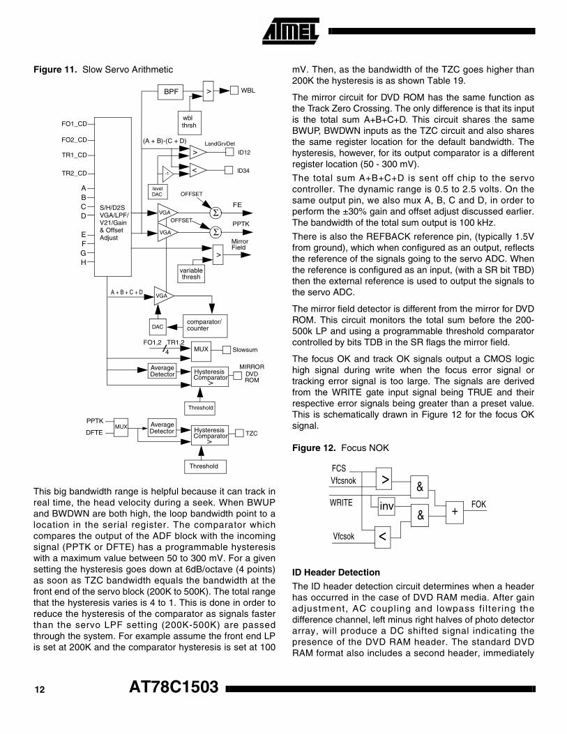
Figure 11. Slow Servo Arithmetic
This big bandwidth range is helpful because it can track inreal time, the head velocity during a seek. When BWUPand BWDWN are both high, the loop bandwidth point to alocation in the serial register. The comparator whichcompares the output of the ADF block with the incomingsignal (PPTK or DFTE) has a programmable hysteresiswith a maximum value between 50 to 300 mV. For a givensetting the hysteresis goes down at 6dB/octave (4 points)as soon as TZC bandwidth equals the bandwidth at thefront end of the servo block (200K to 500K). The total rangethat the hysteresis varies is 4 to 1. This is done in order toreduce the hysteresis of the comparator as signals fasterthan the servo LPF setting (200K-500K) are passedthrough the system. For example assume the front end LPis set at 200K and the comparator hysteresis is set at 100
mV. Then, as the bandwidth of the TZC goes higher than200K the hysteresis is as shown Table 19.
The mirror circuit for DVD ROM has the same function asthe Track Zero Crossing. The only difference is that its inputis the total sum A+B+C+D. This circuit shares the sameBWUP, BWDWN inputs as the TZC circuit and also sharesthe same register location for the default bandwidth. Thehysteresis, however, for its output comparator is a differentregister location (50 - 300 mV).
The total sum A+B+C+D is sent off chip to the servocontroller. The dynamic range is 0.5 to 2.5 volts. On thesame output pin, we also mux A, B, C and D, in order toperform the ±30% gain and offset adjust discussed earlier.The bandwidth of the total sum output is 100 kHz.
There is also the REFBACK reference pin, (typically 1.5Vfrom ground), which when configured as an output, reflectsthe reference of the signals going to the servo ADC. Whenthe reference is configured as an input, (with a SR bit TBD)then the external reference is used to output the signals tothe servo ADC.
The mirror field detector is different from the mirror for DVDROM. This circuit monitors the total sum before the 200-500k LP and using a programmable threshold comparatorcontrolled by bits TDB in the SR flags the mirror field.
The focus OK and track OK signals output a CMOS logichigh signal during write when the focus error signal ortracking error signal is too large. The signals are derivedfrom the WRITE gate input signal being TRUE and theirrespective error signals being greater than a preset value.This is schematically drawn in Figure 12 for the focus OKsignal.
Figure 12. Focus NOK
ID Header Detection
The ID header detection circuit determines when a headerhas occurred in the case of DVD RAM media. After gainadjustment, AC coupl ing and lowpass fi l tering thedifference channel, left minus right halves of photo detectorarray, will produce a DC shifted signal indicating thepresence of the DVD RAM header. The standard DVDRAM format also includes a second header, immediately
VGA
comparator/ DAC
A + B + C + D
FE
PPTK
counter
LandGrvDet
ID12
levelDAC
-1 ID34
>
<
(A + B)-(C + D)
BPF WBL
wbl thrsh
>
Slowsum
MIRRORDVDROM
>
variablethresh
MirrorField
MUX4
FO1,2 TR1,2
AverageDetector
>
HysteresisComparator
Threshold
TZCAverageDetector
>
HysteresisComparator
Threshold
MUXPPTK
DFTE
OFFSET
OFFSET
FO1_CD
FO2_CD
TR1_CD
TR2_CD
VGA
VGA
S/H/D2SVGA/LPF/V21/Gain& OffsetAdjust
ABCD
EFGH
Σ
Σ
> &WRITE
VfcsnokFCS
FOK
<Vfcsok
&inv +
AT78C150312
AT78C1503
proceeding the first, with opposite polarity which thedetector will also sense. Once a header occurs, theassertion and deassertion of the ID12 and ID34 pins willcoincide with the detection of the first header and secondheader, respectively. The polarity of the tracking error (TEpin) will also be adjusted to correspond to the properland/groove polarity which is determined by the sign of theDC shift of the first header. The beginning of a header alsocan start a new RF sequence, which will provide the RFdata recovery path with the correctly timed control signals.The RF sequencer is explained in the next section.
The difference signal used by the ID detector is generatedautomatically from the input signals. The difference signalis the sum AP/N+BP/N-(CP/N+DP/N). The differencesignal passes through a fixed gain of 3 V/V before passingthrough a programmable gain stage with transfer functionequal to IDWBLVGA*0.25 V/V. This difference signal isinternally AC coupled with a pole at 2 kHz. The signal thengoes to a 2nd order lowpass filter which has a DC gain of 2V/V. The cutoff frequency of the lowpass filter is set by theIDWBLFLTR<2:0> b i t s and has a va lue o f(IDWBLFLTR+1)*100 kHz which allows for DVD RAM X1through X8 headers to be detected. After filtering, thesignal goes to a window comparator which is clocked at asynthesizer divided by 8 rate. The absolute value of thewindow threshold is set by the IDSLC<3:0> bits and has avalue of IDSLCE*26.2 mV. When the signal exceeds theprogrammed window, it triggers the ID detector statemachine.
The analog signal polarity for ID12 determines if the push-pull tracking error is negated or not, i.e. indicating the startof a land or a groove. If the polarity is positive, then agroove region is being entered and the polarity of thetracking error is not negated. If the polarity of the signal isnegative, then a land region is being entered and the signof the tracking error is negated. The POLPOL bit (Polarityof the Polarity), allows an inversion of the above statedlogic in the case that an inversion has occurred along thesignal path.
The SNGLHDR bit is provided if the media being read hasonly a single header. This allows the ID detector statemachine to be reset following only one header.
The IDINT serial register bit gets logically OR’ed with theIDINT pin which enables the internal ID detector to triggerthe RF sequencer. If neither one of these signals areasserted, the RF sequencer will not be triggered by thedetected header BUT the ID12/ID34 pins are still active asis the polarity switching of the RAM tracking error.
The IDHLD bit allows the part to disable the ID detectorfrom functioning except when the IDSEL pin is asserted.This in effect forces the part to qualify a valid header withthe IDSEL pin. This is helpful once header timing is
acquired and the contro l ler can asser t IDSEL atapproximately the correct time when a header is about tooccur as this prevents possible false triggering of the IDdetector during user data periods.
The IDFLDSRCE bit controls what signal will become theoutput on the IDFIELD pin. When IDFLDSRCE is low, theIDFIELD pin tracks the IDSEL input directly. WhenIDFLDSRCE is high, the IDFIELD output will brought highupon the assertion of ID12 and return low upon thedeassertion of ID34. In the case of SNGLHDR being high,IDFIELD will be brought low upon the deassertion ofID12.This allows the channel to generate its own IDFIELDsignal upon start-up of the system if this signal should berequired by the preamp before the controller knows theexact timing of the RAM headers.
All ID detector functionality will be disabled if the mode con-trol bits, SRVMOD<3:0>, are such that RAM media is notselected.
For test purposes the BY_ACBYP bit is provided whichshorts the signal path around the AC coupling capacitor.This allows DC testing of the ID and Wobble paths.HDRTSTEN allows the ID detector state machine to betested. When asserted, the AGCLZ pin functions as thepositive window comparator output, AGCFST functions asthe negative window comparator output and AGCHLDfunctions as the wobble comparator output. Using thesepins the detector and RF sequencer can be tested by apurely digital means.
RF Sequencer
The RF sequencer provides the capability to internallycontrol the RF paths timing sequence when entering aheader area for RAM or user data for any supported media.The RF signals which it controls are the AGCs’ LOWZ,HOLD and Fast RECovery signals and also the signal toindicate the need to switch to data mode in the timingrecovery block. When enabled, the sequencers outputs arelogically OR’ed with the corresponding external pins and isespecially useful at start-up when the controller doesn’tknow the exact laser position yet.
The sequencer may be started in several ways, all of whichmay be enabled or disabled. In DVD RAM header mode,the sequencer may be started with the assertion of theinternally generated ID12 and ID34 or the external input pinIDSEL. The choice of which mode the sequencer startswith is determined by the state of the ID internal (IDINT)pin. If IDINT is asserted, logically high, the internally gener-ated ID12 signal is used to start the sequencer. This isuseful under the condition that the controller does not yetknow the laser location, or the controller does not containthe circuitry required to generate the control signals, or theuser believes the channel can more accurately detect the
13

headers than the controller can time them. If IDINT is notasserted, it is set logically low, then the external pin IDSELmay be used to start the RF sequencer. This mode is use-ful if the controller does not contain the required logic togenerate the RF signals or if fewer inter-connects betweenthe controller and channel were desired. In all types ofmedia, the RF sequencer may also be started with theassertion of the pin RG.
The RF sequencers system clock is derived from the fre-quency synthesizer divided by four so it is thereforeclocked at a nibble rate with respect to the RF channel rate.As stated above, the start signal for the sequencer can beone of several possibilities. The lengths of each timing fieldare user programmable and are all stated in terms of nibblerate. Figure 1 shows the generated signals and the amountof programmability for each field.
LOWZ/HOLD line is shown starting asserted. This wouldbe the typical case when entering a RAM header or a userdata field. As stated above, the start signal can be eitherthe RG pin or one of several ID header indicators. In thecase of RAM headers, the LOWZ needs to be asserted inorder for the on-chip AC Coupling to reject the large DCshift present in the header. Once the DC shift has passed,the AC coupling pole is internally reduced at a controlledrate in order for no DC offset to be stored on the ACcoupling capacitors. The amount of time to allow the ACcoupling pole to be brought down is controlled by theACCPLTM bits. Once the pole has been reduced an AGCfast attack mode is entered. The details of this mode areexplained in the AGC section. The amount of time toremain in this state is controlled by the AGCFSTTM bits.After the AGCFSTTM has timed out, the DC restore blockand timing recovery PLL are allowed to begin reading userdata. The RSTTM allows the sequencer to deassert theID12/ID34 lines. This is useful when the exact length ofheaders are known so that the analog ID detector does notneed to accurately detect the end of the RAM headers.
There are several other control bits for the sequencerwhich will now be described. For standard DVD RAMmedia there are two DC shifted headers immediately fol-lowing one another. For non-standard RAM media, whereonly a single header is present, the SNGLHDR bit shouldbe programmed high. This allows the sequencer to onlytime-out a single header, rather than the assumed two
headers. This feature is used when the HDRATMG,(Header Auto-timing Bit), is asserted. When the auto timingfeature is enabled, only the leading edge of the header, i.e.ID12, needs to be accurately detected by the ID detector.Since the user knows the exact length of the headers onthe media, the RSTTM can be programmed to accuratelyput the RF path in LOWZ mode when the header is com-pleted. This is useful since the analog detector may besusceptible to noise and ma,y therefore, not time-out at theexact time. When in double header mode, SNGLHDR=0,the sequencer will automatically generate the second RFsequence when headers 3/4 are present independent ofID34 signal.
The RAMREAD bit allows an internal signal which controlsthe source for the timing recovery to be controlled by thesequencer to properly set the reference for the timingrecovery when reading RAM media. This bit needs to beprogrammed low when a RAM data read operation is firststarted and then may be programmed high while readingRAM data. When RAMREAD is high, the timing recoveryPLL will automatically go into a phase/frequency modewhen entering a header. This allows very fast frequencyacquisition onto the preamble present at the beginning ofRAM headers. The sequencer will also automatically putthe timing recovery into a coast mode between headersand also in the gap fields present at the beginning and endof the headers, before and after user data.
The sequencer can also produce the required timingsequence off the leading edge of RG when RGSTRT, RGstart, bit is low. When this bit is high, no sequence will begenerated from the leading edge of RG and it is assumedthat the controller is providing the proper AGC timingsignals.
The DATREFST, (Data Reference Start Bit), allows theinternal signal, which controls the reference, either thesynthesizer or data, for the timing recovery to come directlyfrom the IDFIELD or RG pins when DATREFST is high.This will effectively bypass all sequencer signals whichcontrol the timing recovery block. A DISSQCR bit is alsoprovided to disable the entire sequencer when it isprogrammed high.
When not in RAM mode, internal logic will also prevent thesequencer from starting on any other signal other than RG.
AT78C150314
AT78C1503
Figure 13. RF Path Timing Sequence
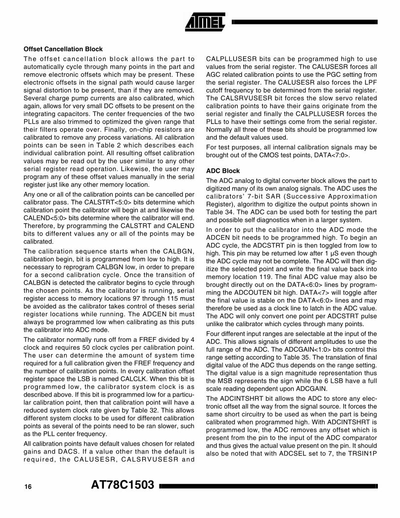
Wobble Signal Detect
The wobble signal passes through the same signal path asthe ID header signal up through the AC coupling. Thewobble signal is extracted with a bandpass filter, 2 zerosand three poles. While operating with DVD RAM media thefilter passband is centered at (IDWBLFLTR+1)*157 KHzwith 20 dB of passband gain. The center of the bandpassfilter for DVD+RW media the passband is centered at(IDWBLFLTR+1)*817.5 KHz. The output of the fifth orderbandpass filter is the input to the Wobble PLL block. Ablock diagram is shown in Figure 1. The output of thebandpass filter is the input to the Wobble Clock generationblock and to a threshold comparator which is compared tothe WBLLVL<1:0> setting. The output of the comparator isclocked with the 2X wobble clock, which is derived from thewobble signal squared. If the output of the bandpass filter islarger than the programmed level the output of theWOBBLE data flip-flop will be high. The input of the flip-flop
and output are input to an XOR gate to determine thephase transitions in the ADIP signal.
The comparator trip point is determined by a combinationof the WBL EN bit and WBL<1:0>. If WBL EN is low, thenthe comparators reference level is set to zero and theWOBBLE signal appears ideally with a 50/50 duty cycle,during the monotone wobble signal, and will detect the. IfWBL EN is high, then the comparator’s trip point is shiftedfrom zero to the value shown in Table 33.
The BLKWBL bit allows the wobble pin to be held low whilereading through a DVD RAM header. The HDRTSTEN,header test enable bit, allows the wobble path logic to betested. When it is programmed high, the AGCHLD pin willappear at the WOBBLE pin output. The WOBBLE signalwill be disabled if not in a DVD RAM mode, see Table 27.
Figure 14. Wobble PLL Block Diagram
Start Signal
LOWZ/HOLD
1-15 Clocks (AGCLZTM<3:0>)
AC Coupling Recovery
1-63 Clocks (ACCPLTM<5:0>)
RF Sequencer Reset
1-255 Clocks (RSTTM<7:0>)
1-63 Clocks (AGCFSTTM<5:0>)
AGC Fast
A+B-(C+D)
BP1 ( )2
PDBP2 VCO
Delay
HysteresisComparator
Loopfilter
T-FF
D-FF
WobbleClock
WobbleData
XOR
15
Offset Cancellation Block
The o f fse t cance l la t i on b lock a l lows the par t toautomatically cycle through many points in the part andremove electronic offsets which may be present. Theseelectronic offsets in the signal path would cause largersignal distortion to be present, than if they are removed.Several charge pump currents are also calibrated, whichagain, allows for very small DC offsets to be present on theintegrating capacitors. The center frequencies of the twoPLLs are also trimmed to optimized the given range thattheir filters operate over. Finally, on-chip resistors arecalibrated to remove any process variations. All calibrationpoints can be seen in Table 2 which describes eachindividual calibration point. All resulting offset calibrationvalues may be read out by the user similar to any otherserial register read operation. Likewise, the user mayprogram any of these offset values manually in the serialregister just like any other memory location.
Any one or all of the calibration points can be cancelled percalibrator pass. The CALSTRT<5:0> bits determine whichcalibration point the calibrator will begin at and likewise theCALEND<5:0> bits determine where the calibrator will end.Therefore, by programming the CALSTRT and CALENDbits to different values any or all of the points may becalibrated.
The calibration sequence starts when the CALBGN,calibration begin, bit is programmed from low to high. It isnecessary to reprogram CALBGN low, in order to preparefor a second calibration cycle. Once the transition ofCALBGN is detected the calibrator begins to cycle throughthe chosen points. As the calibrator is running, serialregister access to memory locations 97 through 115 mustbe avoided as the calibrator takes control of theses serialregister locations while running. The ADCEN bit mustalways be programmed low when calibrating as this putsthe calibrator into ADC mode.
The calibrator normally runs off from a FREF divided by 4clock and requires 50 clock cycles per calibration point.The user can determine the amount of system timerequired for a full calibration given the FREF frequency andthe number of calibration points. In every calibration offsetregister space the LSB is named CALCLK. When this bit isprogrammed low, the calibrator system clock is asdescribed above. If this bit is programmed low for a particu-lar calibration point, then that calibration point will have areduced system clock rate given by Table 32. This allowsdifferent system clocks to be used for different calibrationpoints as several of the points need to be ran slower, suchas the PLL center frequency.
All calibration points have default values chosen for relatedgains and DACS. If a value other than the default isrequ i red , the CALUSESR, CALSRVUSESR and
CALPLLUSESR bits can be programmed high to usevalues from the serial register. The CALUSESR forces allAGC related calibration points to use the PGC setting fromthe serial register. The CALUSESR also forces the LPFcutoff frequency to be determined from the serial register.The CALSRVUSESR bit forces the slow servo relatedcalibration points to have their gains originate from theserial register and finally the CALPLLUSESR forces thePLLs to have their settings come from the serial register.Normally all three of these bits should be programmed lowand the default values used.
For test purposes, all internal calibration signals may bebrought out of the CMOS test points, DATA<7:0>.
ADC Block
The ADC analog to digital converter block allows the part todigitized many of its own analog signals. The ADC uses thecal ibrators ’ 7-bit SAR (Successive ApproximationRegister), algorithm to digitize the output points shown inTable 34. The ADC can be used both for testing the partand possible self diagnostics when in a larger system.
In order to put the calibrator into the ADC mode theADCEN bit needs to be programmed high. To begin anADC cycle, the ADCSTRT pin is then toggled from low tohigh. This pin may be returned low after 1 µS even thoughthe ADC cycle may not be complete. The ADC will then dig-itize the selected point and write the final value back intomemory location 119. The final ADC value may also bebrought directly out on the DATA<6:0> lines by program-ming the ADCOUTEN bit high. DATA<7> will toggle afterthe final value is stable on the DATA<6:0> lines and maytherefore be used as a clock line to latch in the ADC value.The ADC will only convert one point per ADCSTRT pulseunlike the calibrator which cycles through many points.
Four different input ranges are selectable at the input of theADC. This allows signals of different amplitudes to use thefull range of the ADC. The ADCGAIN<1:0> bits control thisrange setting according to Table 35. The translation of finaldigital value of the ADC thus depends on the range setting.The digital value is a sign magnitude representation thusthe MSB represents the sign while the 6 LSB have a fullscale reading dependent upon ADCGAIN.
The ADCINTSHRT bit allows the ADC to store any elec-tronic offset all the way from the signal source. It forces thesame short circuitry to be used as when the part is beingcalibrated when programmed high. With ADCINTSHRT isprogrammed low, the ADC removes any offset which ispresent from the pin to the input of the ADC comparatorand thus gives the actual value present on the pin. It shouldalso be noted that with ADCSEL set to 7, the TRSIN1P
AT78C150316
AT78C1503
input is selected which allows for any external signal to beconverted.
In conjunction with the ADC function which digitizes variousoutputs, the part also has the capability to force DC offsetvoltages at all the signal inputs. This is very useful for DCtests in which many of the internal gains gain can beverified with no external hardware. A DC value can beforced at the input and the resulting output at any of the testpoints can be digitized by the ADC and read out the serialregister interface. The FORCEVIN, force voltage input, bit
enables current sources and switches the input ACcoupling blocks to generate zero TC voltages. While this bitis programmed high, no attempt should be made to use thepart with actual data. The FORCESEL<2:0> bits determinewhich input will have the offset voltage on it, see Table 36.The amount of offset is determined by FORCEVAL<2:0>bits, see Table 37. Since the RF path and the slow servopath internally use different input stages, their respectiveoffset voltages are different as shown with the two separatecolumns in Table 37.
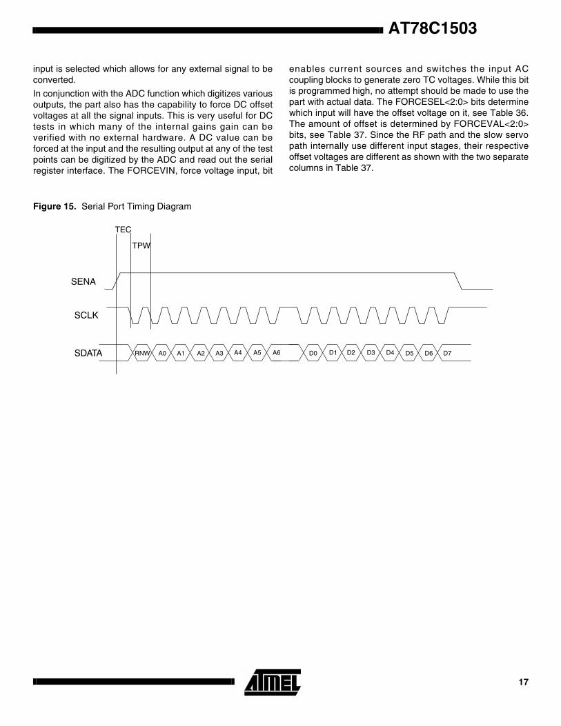
Figure 15. Serial Port Timing Diagram
SENA
SCLK
RNW A0 A1 A2 A3 A4 A5 A6 D0 D1 D2 D3 D4 D5 D6 D7SDATA
TEC
TPW
17
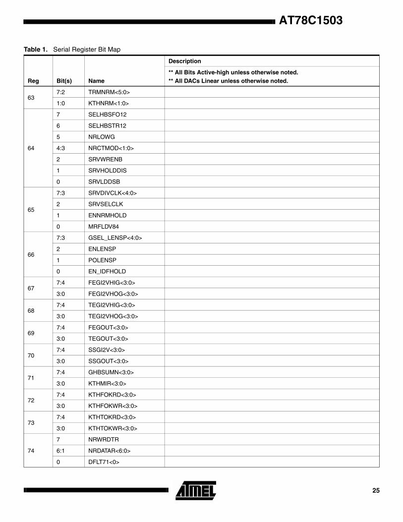
*Disclaimer to users of this table. The location of some (if not all) of the bits in this serial register will probably change. Writeyour code in order to minimize the impact of such changes, e.g., define these bit locations in only one place in yourprogram.
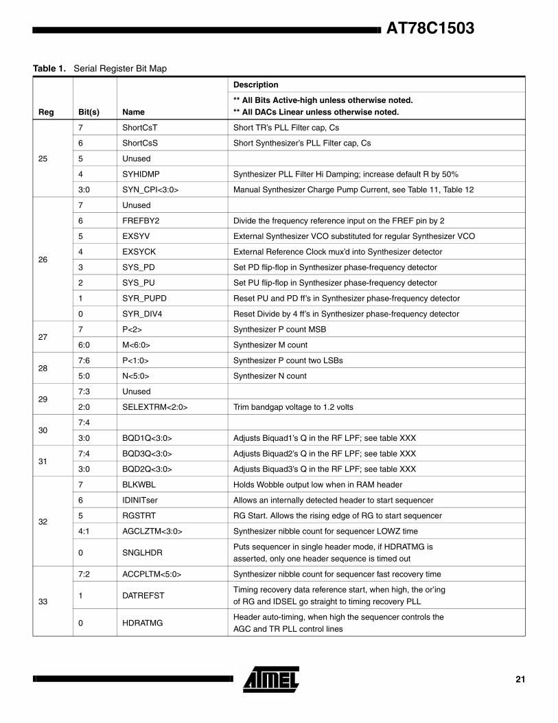
Table 1. Serial Register Bit Map
Reg Bit(s) Name
Description
** All Bits Active-high unless otherwise noted.** All DACs Linear unless otherwise noted.
0
7 AGCCALTPONEnable cal test point selection, disable TP1<5:0> from controlling the outputs on TP1 respectively
6 TP1EN Test Point 1 Enable
5:0 TP1ser<5:0> Test Point 1 (AGC) Selection; see Table 6
1
7 Unused
6 TP2EN Test Point 2 Enable
5:0 TP2ser<5:0> Test Point 2 (LPF) Selection; see Table 8
2
7 DETSHRTR Short a 60k resistor across the detector charge pump output
6 TSDDEN Test Point TSDD1 & TSDD2 Enable
5:0 TSDD1ser<5:0> Test Point TSDD1 (DCR, DPD, TR) Selection; see Table 18
3
7 Unused
6 TPSHRTser Short all test points
5:0 TSDD2ser<5:0> Test Point TSDD2 (DPD, TR, SYNTH) Selection; see Table 23
47 ACCPL_SLOW
6:0 ANSEser<6:0> Analog Single Ended Selection; see Table 24
5
7 SLEEPser Sleep bit, get OR’d with the PORB pin to power down entire part
6:1 Unused<5:0>
0 PGCEN Programmable Gain Mode Enable for the AGC
6
7:4 AGCQP<3:0> AGC loop charge pump currents; see Table 4
3 FLTRBYP Bypass low-pass filter inside the AGC loop
2 AGCHBW Enable AGC High Band Width mode during fast recovery
1 SQLCHser Squelch
0 Unused
7
7:4 PGC<3:0> Programmable gain magnitude for front-end VGAs; see Table 5
3:2 VGAMODE<1:0> Input range select for front-end VGAs; see Table 3
1 RF_ACBYP Bypass ac-coupling capacitors
0 8P5X_ACBYP Bypass ac-coupling capacitors for the high-gain amplifier
AT78C150318
AT78C1503
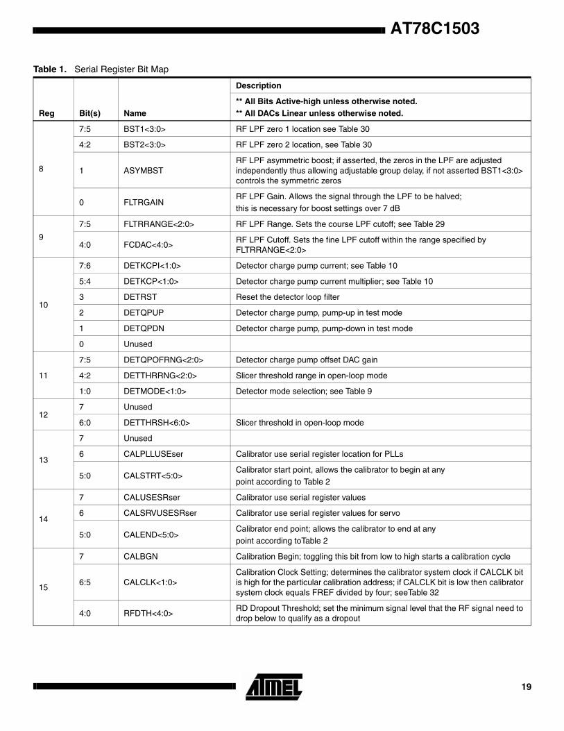
8
7:5 BST1<3:0> RF LPF zero 1 location see Table 30
4:2 BST2<3:0> RF LPF zero 2 location, see Table 30
1 ASYMBSTRF LPF asymmetric boost; if asserted, the zeros in the LPF are adjusted independently thus allowing adjustable group delay, if not asserted BST1<3:0> controls the symmetric zeros
0 FLTRGAINRF LPF Gain. Allows the signal through the LPF to be halved;this is necessary for boost settings over 7 dB
9
7:5 FLTRRANGE<2:0> RF LPF Range. Sets the course LPF cutoff; see Table 29
4:0 FCDAC<4:0>RF LPF Cutoff. Sets the fine LPF cutoff within the range specified by FLTRRANGE<2:0>
10
7:6 DETKCPI<1:0> Detector charge pump current; see Table 10
5:4 DETKCP<1:0> Detector charge pump current multiplier; see Table 10
3 DETRST Reset the detector loop filter
2 DETQPUP Detector charge pump, pump-up in test mode
1 DETQPDN Detector charge pump, pump-down in test mode
0 Unused
11
7:5 DETQPOFRNG<2:0> Detector charge pump offset DAC gain
4:2 DETTHRRNG<2:0> Slicer threshold range in open-loop mode
1:0 DETMODE<1:0> Detector mode selection; see Table 9
127 Unused
6:0 DETTHRSH<6:0> Slicer threshold in open-loop mode
13
7 Unused
6 CALPLLUSEser Calibrator use serial register location for PLLs
5:0 CALSTRT<5:0>Calibrator start point, allows the calibrator to begin at anypoint according to Table 2
14
7 CALUSESRser Calibrator use serial register values
6 CALSRVUSESRser Calibrator use serial register values for servo
5:0 CALEND<5:0>Calibrator end point; allows the calibrator to end at anypoint according toTable 2
15
7 CALBGN Calibration Begin; toggling this bit from low to high starts a calibration cycle
6:5 CALCLK<1:0>Calibration Clock Setting; determines the calibrator system clock if CALCLK bit is high for the particular calibration address; if CALCLK bit is low then calibrator system clock equals FREF divided by four; seeTable 32
4:0 RFDTH<4:0>RD Dropout Threshold; set the minimum signal level that the RF signal need to drop below to qualify as a dropout
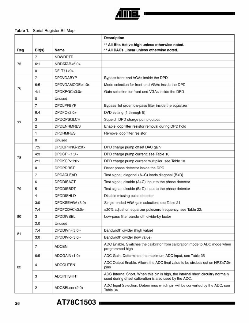
Table 1. Serial Register Bit Map
Reg Bit(s) Name
Description
** All Bits Active-high unless otherwise noted.** All DACs Linear unless otherwise noted.
19
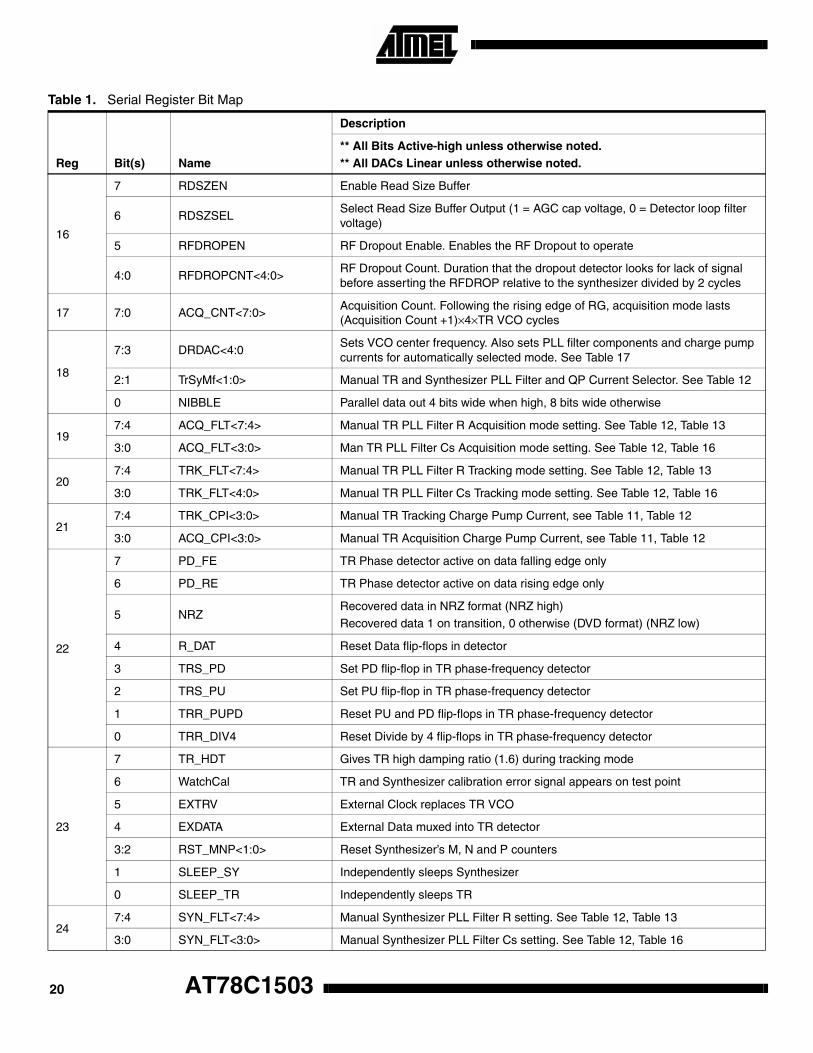
16
7 RDSZEN Enable Read Size Buffer
6 RDSZSELSelect Read Size Buffer Output (1 = AGC cap voltage, 0 = Detector loop filter voltage)
5 RFDROPEN RF Dropout Enable. Enables the RF Dropout to operate
4:0 RFDROPCNT<4:0>RF Dropout Count. Duration that the dropout detector looks for lack of signal before asserting the RFDROP relative to the synthesizer divided by 2 cycles
17 7:0 ACQ_CNT<7:0>Acquisition Count. Following the rising edge of RG, acquisition mode lasts (Acquisition Count +1)×4×TR VCO cycles
18
7:3 DRDAC<4:0Sets VCO center frequency. Also sets PLL filter components and charge pump currents for automatically selected mode. See Table 17
2:1 TrSyMf<1:0> Manual TR and Synthesizer PLL Filter and QP Current Selector. See Table 12
0 NIBBLE Parallel data out 4 bits wide when high, 8 bits wide otherwise
197:4 ACQ_FLT<7:4> Manual TR PLL Filter R Acquisition mode setting. See Table 12, Table 13
3:0 ACQ_FLT<3:0> Man TR PLL Filter Cs Acquisition mode setting. See Table 12, Table 16
207:4 TRK_FLT<7:4> Manual TR PLL Filter R Tracking mode setting. See Table 12, Table 13
3:0 TRK_FLT<4:0> Manual TR PLL Filter Cs Tracking mode setting. See Table 12, Table 16
217:4 TRK_CPI<3:0> Manual TR Tracking Charge Pump Current, see Table 11, Table 12
3:0 ACQ_CPI<3:0> Manual TR Acquisition Charge Pump Current, see Table 11, Table 12
22
7 PD_FE TR Phase detector active on data falling edge only
6 PD_RE TR Phase detector active on data rising edge only
5 NRZRecovered data in NRZ format (NRZ high)Recovered data 1 on transition, 0 otherwise (DVD format) (NRZ low)
4 R_DAT Reset Data flip-flops in detector
3 TRS_PD Set PD flip-flop in TR phase-frequency detector
2 TRS_PU Set PU flip-flop in TR phase-frequency detector
1 TRR_PUPD Reset PU and PD flip-flops in TR phase-frequency detector
0 TRR_DIV4 Reset Divide by 4 flip-flops in TR phase-frequency detector
23
7 TR_HDT Gives TR high damping ratio (1.6) during tracking mode
6 WatchCal TR and Synthesizer calibration error signal appears on test point
5 EXTRV External Clock replaces TR VCO
4 EXDATA External Data muxed into TR detector
3:2 RST_MNP<1:0> Reset Synthesizer’s M, N and P counters
1 SLEEP_SY Independently sleeps Synthesizer
0 SLEEP_TR Independently sleeps TR
247:4 SYN_FLT<7:4> Manual Synthesizer PLL Filter R setting. See Table 12, Table 13
3:0 SYN_FLT<3:0> Manual Synthesizer PLL Filter Cs setting. See Table 12, Table 16
Table 1. Serial Register Bit Map
Reg Bit(s) Name
Description
** All Bits Active-high unless otherwise noted.** All DACs Linear unless otherwise noted.
AT78C150320
AT78C1503
25
7 ShortCsT Short TR’s PLL Filter cap, Cs
6 ShortCsS Short Synthesizer’s PLL Filter cap, Cs
5 Unused
4 SYHIDMP Synthesizer PLL Filter Hi Damping; increase default R by 50%
3:0 SYN_CPI<3:0> Manual Synthesizer Charge Pump Current, see Table 11, Table 12
26
7 Unused
6 FREFBY2 Divide the frequency reference input on the FREF pin by 2
5 EXSYV External Synthesizer VCO substituted for regular Synthesizer VCO
4 EXSYCK External Reference Clock mux’d into Synthesizer detector
3 SYS_PD Set PD flip-flop in Synthesizer phase-frequency detector
2 SYS_PU Set PU flip-flop in Synthesizer phase-frequency detector
1 SYR_PUPD Reset PU and PD ff’s in Synthesizer phase-frequency detector
0 SYR_DIV4 Reset Divide by 4 ff’s in Synthesizer phase-frequency detector
277 P<2> Synthesizer P count MSB
6:0 M<6:0> Synthesizer M count
287:6 P<1:0> Synthesizer P count two LSBs
5:0 N<5:0> Synthesizer N count
297:3 Unused
2:0 SELEXTRM<2:0> Trim bandgap voltage to 1.2 volts
307:4
3:0 BQD1Q<3:0> Adjusts Biquad1’s Q in the RF LPF; see table XXX
317:4 BQD3Q<3:0> Adjusts Biquad2’s Q in the RF LPF; see table XXX
3:0 BQD2Q<3:0> Adjusts Biquad3’s Q in the RF LPF; see table XXX
32
7 BLKWBL Holds Wobble output low when in RAM header
6 IDINITser Allows an internally detected header to start sequencer
5 RGSTRT RG Start. Allows the rising edge of RG to start sequencer
4:1 AGCLZTM<3:0> Synthesizer nibble count for sequencer LOWZ time
0 SNGLHDRPuts sequencer in single header mode, if HDRATMG isasserted, only one header sequence is timed out
33
7:2 ACCPLTM<5:0> Synthesizer nibble count for sequencer fast recovery time
1 DATREFSTTiming recovery data reference start, when high, the or’ing
of RG and IDSEL go straight to timing recovery PLL
0 HDRATMGHeader auto-timing, when high the sequencer controls the
AGC and TR PLL control lines
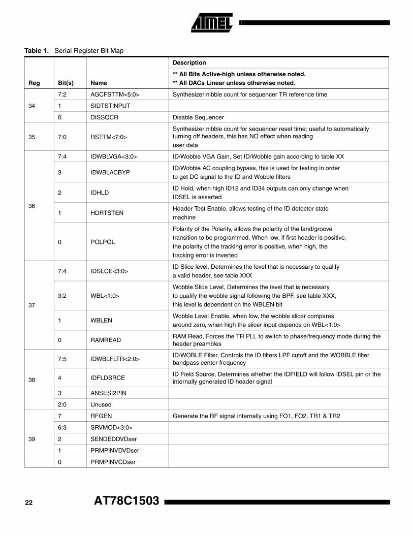
Table 1. Serial Register Bit Map
Reg Bit(s) Name
Description
** All Bits Active-high unless otherwise noted.** All DACs Linear unless otherwise noted.
21
34
7:2 AGCFSTTM<5:0> Synthesizer nibble count for sequencer TR reference time
1 SIDTSTINPUT
0 DISSQCR Disable Sequencer
35 7:0 RSTTM<7:0>Synthesizer nibble count for sequencer reset time; useful to automatically turning off headers, this has NO effect when reading
user data
36
7:4 IDWBLVGA<3:0> ID/Wobble VGA Gain, Set ID/Wobble gain according to table XX
3 IDWBLACBYPID/Wobble AC coupling bypass, this is used for testing in orderto get DC signal to the ID and Wobble filters
2 IDHLDID Hold, when high ID12 and ID34 outputs can only change whenIDSEL is asserted
1 HDRTSTENHeader Test Enable, allows testing of the ID detector statemachine
0 POLPOL
Polarity of the Polarity, allows the polarity of the land/groovetransition to be programmed. When low, if first header is positive,
the polarity of the tracking error is positive, when high, thetracking error is inverted
37
7:4 IDSLCE<3:0>ID Slice level, Determines the level that is necessary to qualifya valid header, see table XXX
3:2 WBL<1:0>Wobble Slice Level, Determines the level that is necessaryto qualify the wobble signal following the BPF, see table XXX,this level is dependent on the WBLEN bit
1 WBLENWobble Level Enable, when low, the wobble slicer comparesaround zero, when high the slicer input depends on WBL<1:0>
0 RAMREADRAM Read, Forces the TR PLL to switch to phase/frequency mode during the header preambles
38
7:5 IDWBLFLTR<2:0>ID/WOBLE Filter, Controls the ID filters LPF cutoff and the WOBBLE filter bandpass center frequency
4 IDFLDSRCEID Field Source, Determines whether the IDFIELD will follow IDSEL pin or the internally generated ID header signal
3 ANSESI2PIN
2:0 Unused
39
7 RFGEN Generate the RF signal internally using FO1, FO2, TR1 & TR2
6:3 SRVMOD<3:0>
2 SENDEDDVDser
1 PRMPINVDVDser
0 PRMPINVCDser
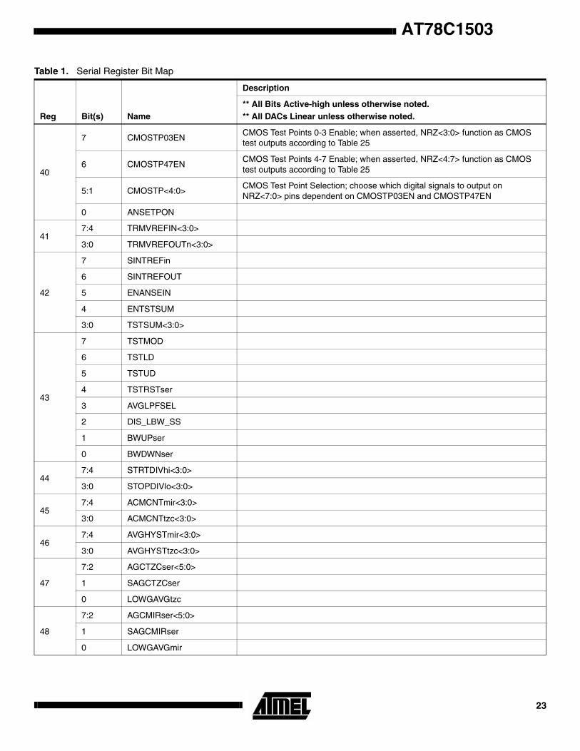
Table 1. Serial Register Bit Map
Reg Bit(s) Name
Description
** All Bits Active-high unless otherwise noted.** All DACs Linear unless otherwise noted.
AT78C150322
AT78C1503
40
7 CMOSTP03ENCMOS Test Points 0-3 Enable; when asserted, NRZ<3:0> function as CMOS test outputs according to Table 25
6 CMOSTP47ENCMOS Test Points 4-7 Enable; when asserted, NRZ<4:7> function as CMOS test outputs according to Table 25
5:1 CMOSTP<4:0>CMOS Test Point Selection; choose which digital signals to output on NRZ<7:0> pins dependent on CMOSTP03EN and CMOSTP47EN
0 ANSETPON
417:4 TRMVREFIN<3:0>
3:0 TRMVREFOUTn<3:0>
42
7 SINTREFin
6 SINTREFOUT
5 ENANSEIN
4 ENTSTSUM
3:0 TSTSUM<3:0>
43
7 TSTMOD
6 TSTLD
5 TSTUD
4 TSTRSTser
3 AVGLPFSEL
2 DIS_LBW_SS
1 BWUPser
0 BWDWNser
447:4 STRTDIVhi<3:0>
3:0 STOPDIVlo<3:0>
457:4 ACMCNTmir<3:0>
3:0 ACMCNTtzc<3:0>
467:4 AVGHYSTmir<3:0>
3:0 AVGHYSTtzc<3:0>
47
7:2 AGCTZCser<5:0>
1 SAGCTZCser
0 LOWGAVGtzc
48
7:2 AGCMIRser<5:0>
1 SAGCMIRser
0 LOWGAVGmir
Table 1. Serial Register Bit Map
Reg Bit(s) Name
Description
** All Bits Active-high unless otherwise noted.** All DACs Linear unless otherwise noted.
23
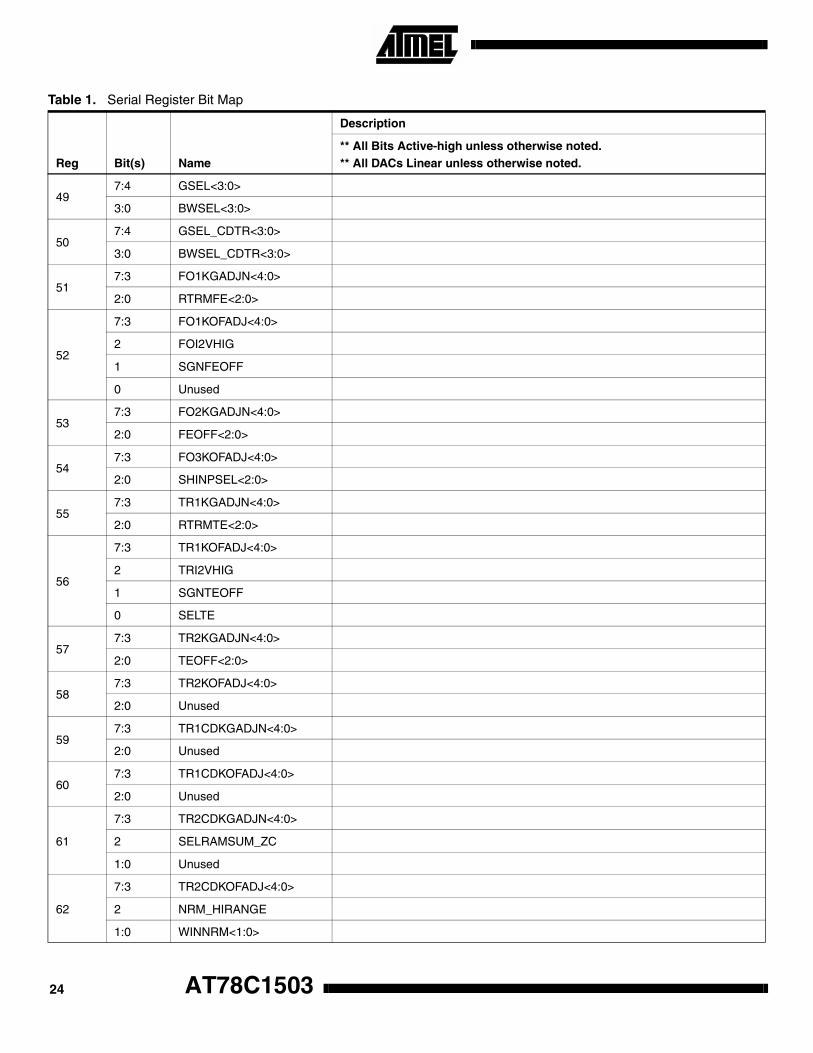
497:4 GSEL<3:0>
3:0 BWSEL<3:0>
507:4 GSEL_CDTR<3:0>
3:0 BWSEL_CDTR<3:0>
517:3 FO1KGADJN<4:0>
2:0 RTRMFE<2:0>
52
7:3 FO1KOFADJ<4:0>
2 FOI2VHIG
1 SGNFEOFF
0 Unused
537:3 FO2KGADJN<4:0>
2:0 FEOFF<2:0>
547:3 FO3KOFADJ<4:0>
2:0 SHINPSEL<2:0>
557:3 TR1KGADJN<4:0>
2:0 RTRMTE<2:0>
56
7:3 TR1KOFADJ<4:0>
2 TRI2VHIG
1 SGNTEOFF
0 SELTE
577:3 TR2KGADJN<4:0>
2:0 TEOFF<2:0>
587:3 TR2KOFADJ<4:0>
2:0 Unused
597:3 TR1CDKGADJN<4:0>
2:0 Unused
607:3 TR1CDKOFADJ<4:0>
2:0 Unused
61
7:3 TR2CDKGADJN<4:0>
2 SELRAMSUM_ZC
1:0 Unused
62
7:3 TR2CDKOFADJ<4:0>
2 NRM_HIRANGE
1:0 WINNRM<1:0>
Table 1. Serial Register Bit Map
Reg Bit(s) Name
Description
** All Bits Active-high unless otherwise noted.** All DACs Linear unless otherwise noted.
AT78C150324
AT78C1503
637:2 TRMNRM<5:0>
1:0 KTHNRM<1:0>
64
7 SELHBSFO12
6 SELHBSTR12
5 NRLOWG
4:3 NRCTMOD<1:0>
2 SRVWRENB
1 SRVHOLDDIS
0 SRVLDDSB
65
7:3 SRVDIVCLK<4:0>
2 SRVSELCLK
1 ENNRMHOLD
0 MRFLDV84
66
7:3 GSEL_LENSP<4:0>
2 ENLENSP
1 POLENSP
0 EN_IDFHOLD
677:4 FEGI2VHIG<3:0>
3:0 FEGI2VHOG<3:0>
687:4 TEGI2VHIG<3:0>
3:0 TEGI2VHOG<3:0>
697:4 FEGOUT<3:0>
3:0 TEGOUT<3:0>
707:4 SSGI2V<3:0>
3:0 SSGOUT<3:0>
717:4 GHBSUMN<3:0>
3:0 KTHMIR<3:0>
727:4 KTHFOKRD<3:0>
3:0 KTHFOKWR<3:0>
737:4 KTHTOKRD<3:0>
3:0 KTHTOKWR<3:0>
74
7 NRWRDTR
6:1 NRDATAR<6:0>
0 DFLT71<0>
Table 1. Serial Register Bit Map
Reg Bit(s) Name
Description
** All Bits Active-high unless otherwise noted.** All DACs Linear unless otherwise noted.
25
75
7 NRWRDTR
6:1 NRDATAR<6:0>
0 DFLT71<0>
76
7 DPDVGABYP Bypass front-end VGAs inside the DPD
6:5 DPDVGAMODE<1:0> Mode selection for front-end VGAs inside the DPD
4:1 DPDKPGC<3:0> Gain selection for front-end VGAs inside the DPD
0 Unused
77
7 DPDLPFBYP Bypass 1st order low-pass filter inside the equalizer
6:4 DPDFC<2:0> DVD setting (1 through 5)
3 DPDQPSQLCH Squelch DPD charge pump output
2 DPDENRMRES Enable loop filter resistor removal during DPD hold
1 DPDRMRES Remove loop filter resistor
0 Unused
78
7:5 DPDQPRNG<2:0> DPD charge pump offset DAC gain
4:3 DPDCPI<1:0> DPD charge pump current; see Table 10
2:1 DPDKCP<1:0> DPD charge pump current multiplier; see Table 10
0 DPDPDRST Reset phase detector inside the DPD
79
7 DPDACLEAD Test signal; diagonal (A+C) leads diagonal (B+D)
6 DPDDISACT Test signal; disable (A+C) input to the phase detector
5 DPDDISBDT Test signal; disable (B+D) input to the phase detector
4 DPDDISHLD Disable missing pulse detector
3:0 DPDKSEVGA<3:0> Single-ended VGA gain selection; see Table 21
80
7:4 DPDFCDAC<3:0> ±20% adjust on equalizer pole/zero frequency; see Table 22;
3 DPDDIVSEL Low-pass filter bandwidth divide-by factor
2:0 Unused
817:4 DPDDIVhi<3:0> Bandwidth divider (high value)
3:0 DPDDIVlo<3:0> Bandwidth divider (low value)
82
7 ADCENADC Enable. Switches the calibrator from calibration mode to ADC mode when programmed high
6:5 ADCGAIN<1:0> ADC Gain. Determines the maximum ADC input, see Table 35
4 ADCOUTENADC Output Enable. Allows the ADC final value to be strobes out on NRZ<7:0> pins
3 ADCINTSHRTADC Internal Short. When this pin is high, the internal short circuitry normally used during offset calibration is also used by the ADC.
2 ADCSELser<2:0>ADC Input Selection. Determines which pin will be converted by the ADC, see Table 34
Table 1. Serial Register Bit Map
Reg Bit(s) Name
Description
** All Bits Active-high unless otherwise noted.** All DACs Linear unless otherwise noted.
AT78C150326
AT78C1503
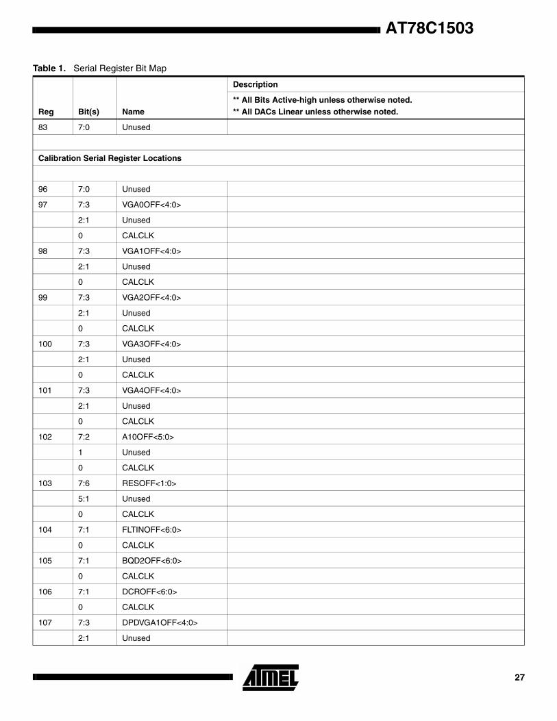
83 7:0 Unused
Calibration Serial Register Locations
96 7:0 Unused
97 7:3 VGA0OFF<4:0>
2:1 Unused
0 CALCLK
98 7:3 VGA1OFF<4:0>
2:1 Unused
0 CALCLK
99 7:3 VGA2OFF<4:0>
2:1 Unused
0 CALCLK
100 7:3 VGA3OFF<4:0>
2:1 Unused
0 CALCLK
101 7:3 VGA4OFF<4:0>
2:1 Unused
0 CALCLK
102 7:2 A10OFF<5:0>
1 Unused
0 CALCLK
103 7:6 RESOFF<1:0>
5:1 Unused
0 CALCLK
104 7:1 FLTINOFF<6:0>
0 CALCLK
105 7:1 BQD2OFF<6:0>
0 CALCLK
106 7:1 DCROFF<6:0>
0 CALCLK
107 7:3 DPDVGA1OFF<4:0>
2:1 Unused
Table 1. Serial Register Bit Map
Reg Bit(s) Name
Description
** All Bits Active-high unless otherwise noted.** All DACs Linear unless otherwise noted.
27
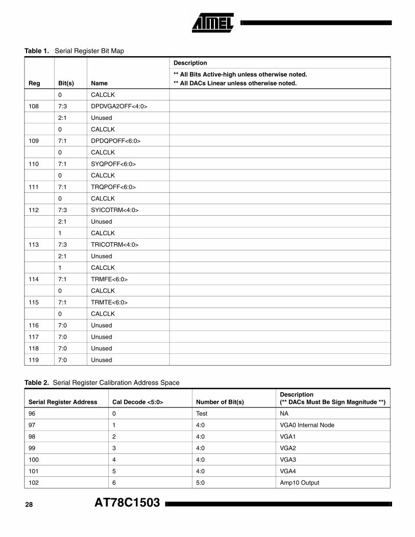
0 CALCLK
108 7:3 DPDVGA2OFF<4:0>
2:1 Unused
0 CALCLK
109 7:1 DPDQPOFF<6:0>
0 CALCLK
110 7:1 SYQPOFF<6:0>
0 CALCLK
111 7:1 TRQPOFF<6:0>
0 CALCLK
112 7:3 SYICOTRM<4:0>
2:1 Unused
1 CALCLK
113 7:3 TRICOTRM<4:0>
2:1 Unused
1 CALCLK
114 7:1 TRMFE<6:0>
0 CALCLK
115 7:1 TRMTE<6:0>
0 CALCLK
116 7:0 Unused
117 7:0 Unused
118 7:0 Unused
119 7:0 Unused
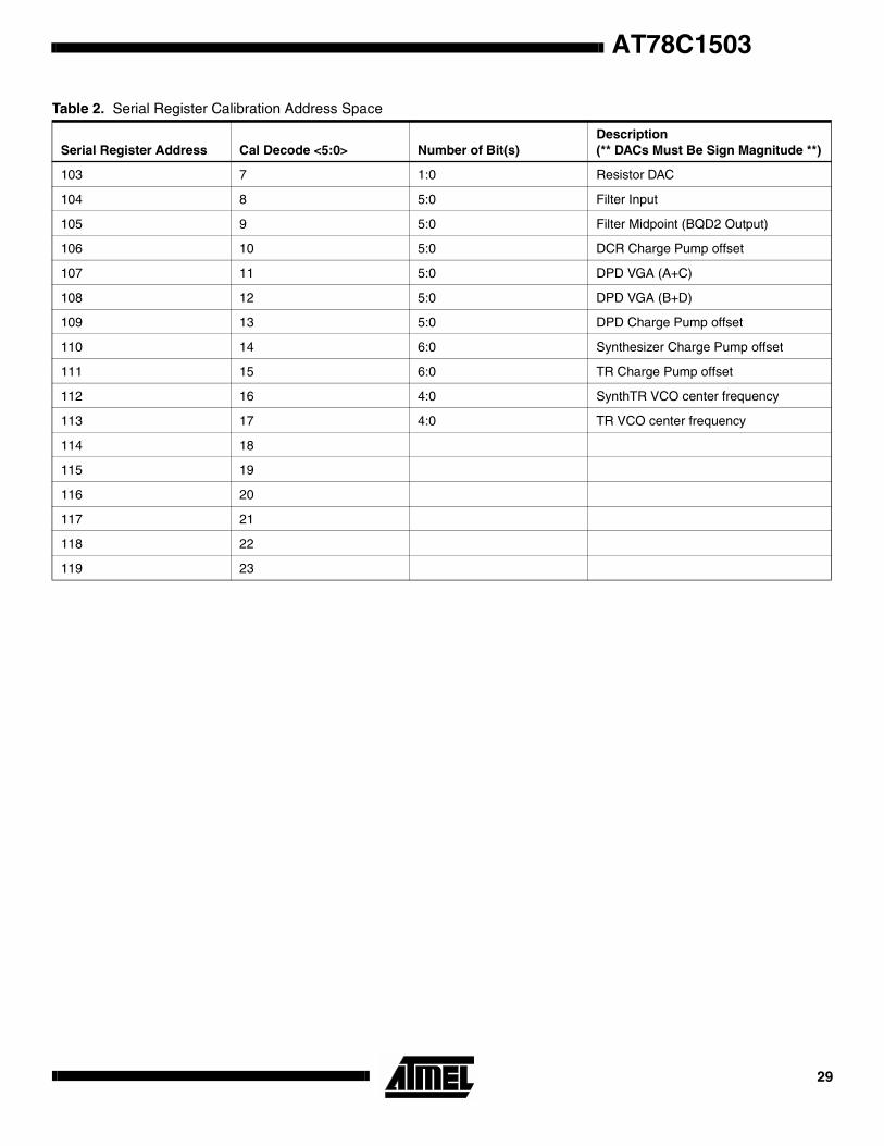
Table 2. Serial Register Calibration Address Space
Serial Register Address Cal Decode <5:0> Number of Bit(s)Description(** DACs Must Be Sign Magnitude **)
96 0 Test NA
97 1 4:0 VGA0 Internal Node
98 2 4:0 VGA1
99 3 4:0 VGA2
100 4 4:0 VGA3
101 5 4:0 VGA4
102 6 5:0 Amp10 Output
Table 1. Serial Register Bit Map
Reg Bit(s) Name
Description
** All Bits Active-high unless otherwise noted.** All DACs Linear unless otherwise noted.
AT78C150328
AT78C1503
103 7 1:0 Resistor DAC
104 8 5:0 Filter Input
105 9 5:0 Filter Midpoint (BQD2 Output)
106 10 5:0 DCR Charge Pump offset
107 11 5:0 DPD VGA (A+C)
108 12 5:0 DPD VGA (B+D)
109 13 5:0 DPD Charge Pump offset
110 14 6:0 Synthesizer Charge Pump offset
111 15 6:0 TR Charge Pump offset
112 16 4:0 SynthTR VCO center frequency
113 17 4:0 TR VCO center frequency
114 18
115 19
116 20
117 21
118 22
119 23
Table 2. Serial Register Calibration Address Space
Serial Register Address Cal Decode <5:0> Number of Bit(s)Description(** DACs Must Be Sign Magnitude **)
29
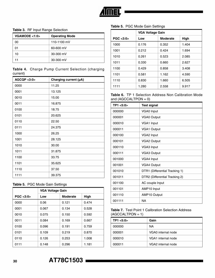
Table 3. RF Input Range Selection
VGAMODE <1:0> Operating Mode
00 110-1100 mV
01 60-600 mV
10 30-300 mV
11 30-300 mV
Table 4. Charge Pump Current Selection (chargingcurrent)
AGCQP <3:0> Charging current (µA)
0000 11.25
0001 13.125
0010 15.00
0011 16.875
0100 18.75
0101 20.625
0110 22.50
0111 24.375
1000 26.25
1001 28.125
1010 30.00
1011 31.875
1100 33.75
1101 35.625
1110 37.50
1111 39.375
Table 5. PGC Mode Gain Settings
PGC <3:0>
VGA Voltage Gain
Low Moderate High
0000 0.06 0.121 0.474
0001 0.067 0.134 0.528
0010 0.075 0.150 0.592
0011 0.084 0.169 0.667
0100 0.096 0.191 0.759
0101 0.109 0.219 0.870
0110 0.126 0.253 1.008
0111 0.148 0.296 1.181
1000 0.176 0.352 1.404
1001 0.212 0.424 1.694
1010 0.261 0.523 2.085
1011 0.330 0.660 2.627
1100 0.429 0.858 3.408
1101 0.581 1.162 4.590
1110 0.830 1.660 6.505
1111 1.280 2.558 9.917
Table 6. TP 1 Selection Address Non Calibration Modeand (AGCCALTPON = 0)
TP1 <5:0> Test signal
000000 VGA0 Input
000001 VGA0 Output
000010 VGA1 Input
000011 VGA1 Output
000100 VGA2 Input
000101 VGA2 Output
000110 VGA3 Input
000111 VGA3 Output
001000 VGA4 Input
001001 VGA4 Output
001010 DTR1 (Differential Tracking 1)
001011 DTR2 (Differential Tracking 2)
001100 AC couple Input
001101 AMP10 Input
001110 AMP10 Output
001111 NA
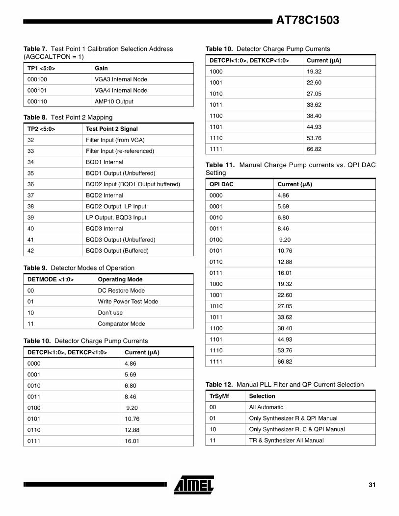
Table 7. Test Point 1 Calibration Selection Address (AGCCALTPON = 1)
TP1 <5:0> Gain
000000 NA
000001 VGA0 internal node
000010 VGA1 internal node
000011 VGA2 internal node
Table 5. PGC Mode Gain Settings
PGC <3:0>
VGA Voltage Gain
Low Moderate High
AT78C150330
AT78C1503
000100 VGA3 Internal Node
000101 VGA4 Internal Node
000110 AMP10 Output
Table 8. Test Point 2 Mapping
TP2 <5:0> Test Point 2 Signal
32 Filter Input (from VGA)
33 Filter Input (re-referenced)
34 BQD1 Internal
35 BQD1 Output (Unbuffered)
36 BQD2 Input (BQD1 Output buffered)
37 BQD2 Internal
38 BQD2 Output, LP Input
39 LP Output, BQD3 Input
40 BQD3 Internal
41 BQD3 Output (Unbuffered)
42 BQD3 Output (Buffered)
Table 9. Detector Modes of Operation
DETMODE <1:0> Operating Mode
00 DC Restore Mode
01 Write Power Test Mode
10 Don’t use
11 Comparator Mode
Table 10. Detector Charge Pump Currents
DETCPI<1:0>, DETKCP<1:0> Current (µA)
0000 4.86
0001 5.69
0010 6.80
0011 8.46
0100 9.20
0101 10.76
0110 12.88
0111 16.01
Table 7. Test Point 1 Calibration Selection Address (AGCCALTPON = 1)
TP1 <5:0> Gain 1000 19.32
1001 22.60
1010 27.05
1011 33.62
1100 38.40
1101 44.93
1110 53.76
1111 66.82
Table 11. Manual Charge Pump currents vs. QPI DACSetting
QPI DAC Current (µA)
0000 4.86
0001 5.69
0010 6.80
0011 8.46
0100 9.20
0101 10.76
0110 12.88
0111 16.01
1000 19.32
1001 22.60
1010 27.05
1011 33.62
1100 38.40
1101 44.93
1110 53.76
1111 66.82
Table 12. Manual PLL Filter and QP Current Selection
TrSyMf Selection
00 All Automatic
01 Only Synthesizer R & QPI Manual
10 Only Synthesizer R, C & QPI Manual
11 TR & Synthesizer All Manual
Table 10. Detector Charge Pump Currents
DETCPI<1:0>, DETKCP<1:0> Current (µA)
31
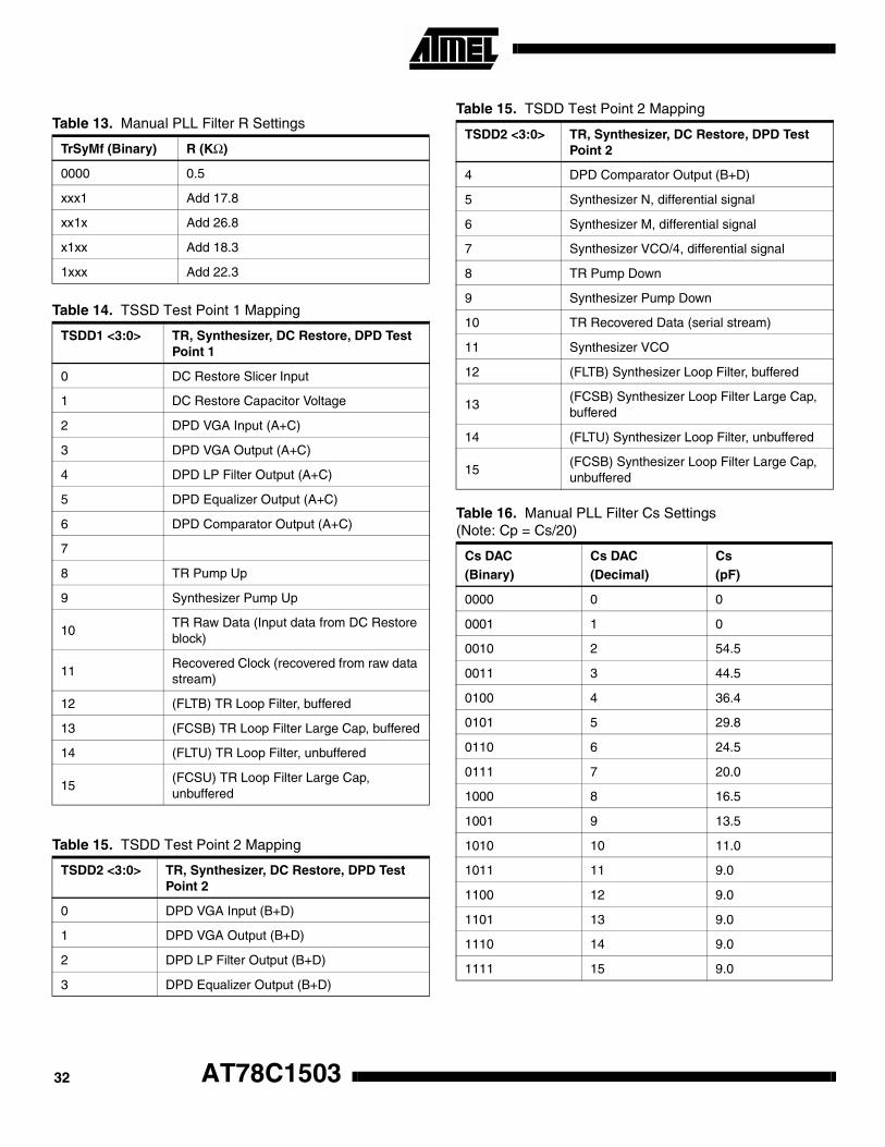
Table 13. Manual PLL Filter R Settings
TrSyMf (Binary) R (KΩ)
0000 0.5
xxx1 Add 17.8
xx1x Add 26.8
x1xx Add 18.3
1xxx Add 22.3
Table 14. TSSD Test Point 1 Mapping
TSDD1 <3:0> TR, Synthesizer, DC Restore, DPD Test Point 1
0 DC Restore Slicer Input
1 DC Restore Capacitor Voltage
2 DPD VGA Input (A+C)
3 DPD VGA Output (A+C)
4 DPD LP Filter Output (A+C)
5 DPD Equalizer Output (A+C)
6 DPD Comparator Output (A+C)
7
8 TR Pump Up
9 Synthesizer Pump Up
10TR Raw Data (Input data from DC Restore block)
11Recovered Clock (recovered from raw data stream)
12 (FLTB) TR Loop Filter, buffered
13 (FCSB) TR Loop Filter Large Cap, buffered
14 (FLTU) TR Loop Filter, unbuffered
15(FCSU) TR Loop Filter Large Cap, unbuffered
Table 15. TSDD Test Point 2 Mapping
TSDD2 <3:0> TR, Synthesizer, DC Restore, DPD Test Point 2
0 DPD VGA Input (B+D)
1 DPD VGA Output (B+D)
2 DPD LP Filter Output (B+D)
3 DPD Equalizer Output (B+D)
4 DPD Comparator Output (B+D)
5 Synthesizer N, differential signal
6 Synthesizer M, differential signal
7 Synthesizer VCO/4, differential signal
8 TR Pump Down
9 Synthesizer Pump Down
10 TR Recovered Data (serial stream)
11 Synthesizer VCO
12 (FLTB) Synthesizer Loop Filter, buffered
13(FCSB) Synthesizer Loop Filter Large Cap, buffered
14 (FLTU) Synthesizer Loop Filter, unbuffered
15(FCSB) Synthesizer Loop Filter Large Cap, unbuffered
Table 16. Manual PLL Filter Cs Settings (Note: Cp = Cs/20)
Cs DAC(Binary)
Cs DAC(Decimal)
Cs (pF)
0000 0 0
0001 1 0
0010 2 54.5
0011 3 44.5
0100 4 36.4
0101 5 29.8
0110 6 24.5
0111 7 20.0
1000 8 16.5
1001 9 13.5
1010 10 11.0
1011 11 9.0
1100 12 9.0
1101 13 9.0
1110 14 9.0
1111 15 9.0
Table 15. TSDD Test Point 2 Mapping
TSDD2 <3:0> TR, Synthesizer, DC Restore, DPD Test Point 2
AT78C150332
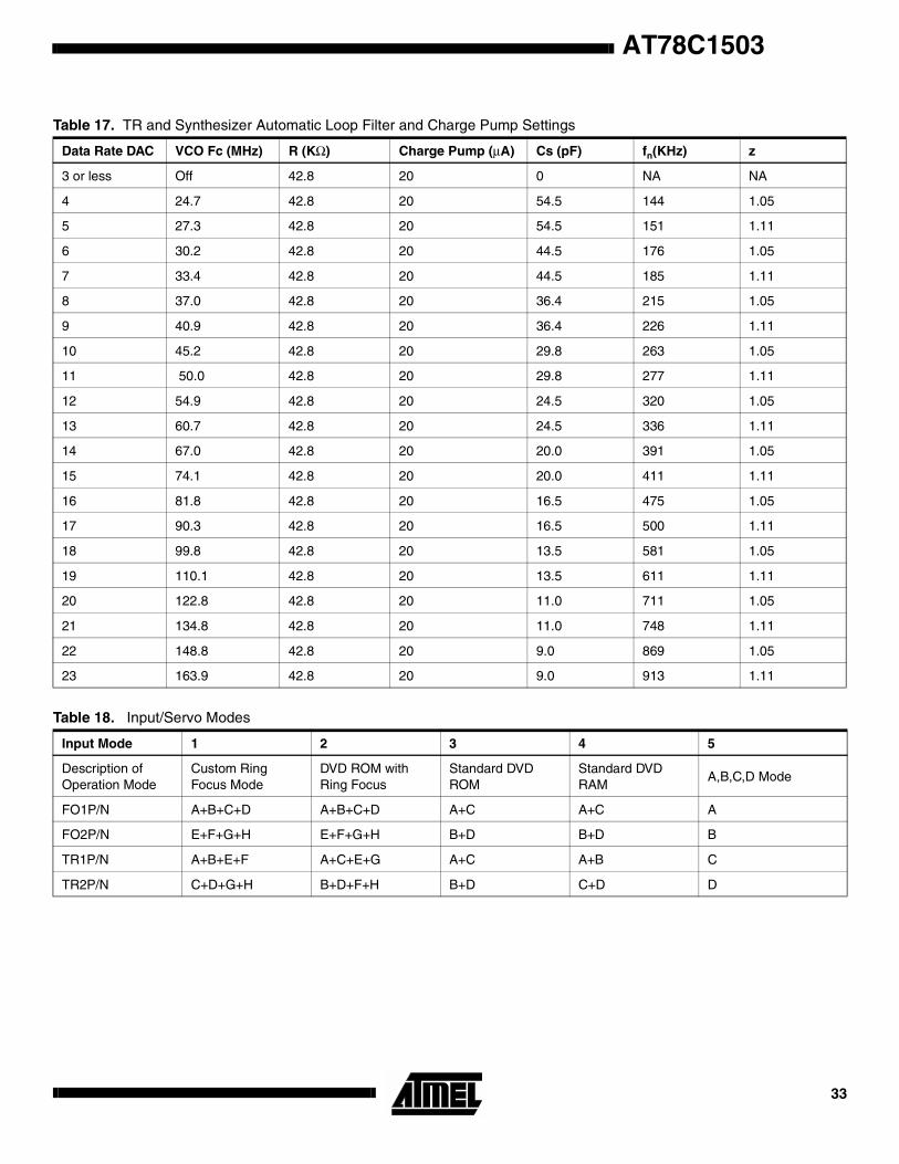
AT78C1503
Table 17. TR and Synthesizer Automatic Loop Filter and Charge Pump Settings
Data Rate DAC VCO Fc (MHz) R (KΩ) Charge Pump (µA) Cs (pF) fn(KHz) z
3 or less Off 42.8 20 0 NA NA
4 24.7 42.8 20 54.5 144 1.05
5 27.3 42.8 20 54.5 151 1.11
6 30.2 42.8 20 44.5 176 1.05
7 33.4 42.8 20 44.5 185 1.11
8 37.0 42.8 20 36.4 215 1.05
9 40.9 42.8 20 36.4 226 1.11
10 45.2 42.8 20 29.8 263 1.05
11 50.0 42.8 20 29.8 277 1.11
12 54.9 42.8 20 24.5 320 1.05
13 60.7 42.8 20 24.5 336 1.11
14 67.0 42.8 20 20.0 391 1.05
15 74.1 42.8 20 20.0 411 1.11
16 81.8 42.8 20 16.5 475 1.05
17 90.3 42.8 20 16.5 500 1.11
18 99.8 42.8 20 13.5 581 1.05
19 110.1 42.8 20 13.5 611 1.11
20 122.8 42.8 20 11.0 711 1.05
21 134.8 42.8 20 11.0 748 1.11
22 148.8 42.8 20 9.0 869 1.05
23 163.9 42.8 20 9.0 913 1.11
Table 18. Input/Servo Modes
Input Mode 1 2 3 4 5
Description of Operation Mode
Custom Ring Focus Mode
DVD ROM with Ring Focus
Standard DVD ROM
Standard DVD RAM
A,B,C,D Mode
FO1P/N A+B+C+D A+B+C+D A+C A+C A
FO2P/N E+F+G+H E+F+G+H B+D B+D B
TR1P/N A+B+E+F A+C+E+G A+C A+B C
TR2P/N C+D+G+H B+D+F+H B+D C+D D
33
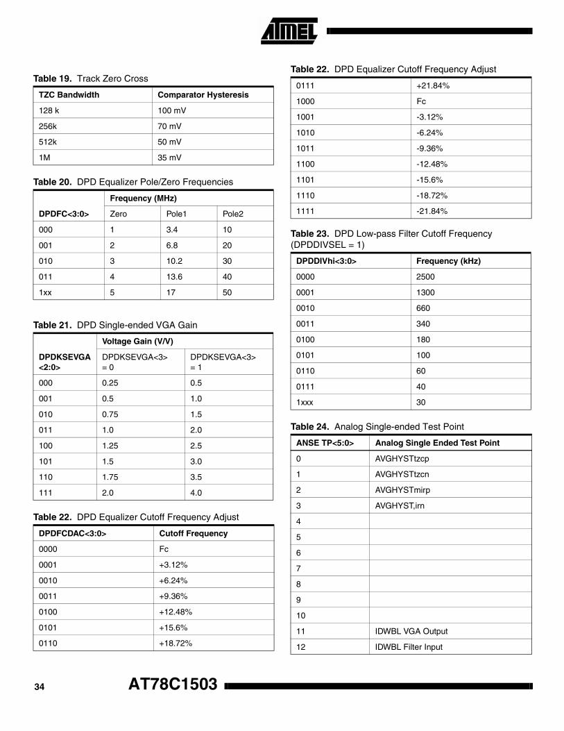
Table 19. Track Zero Cross
TZC Bandwidth Comparator Hysteresis
128 k 100 mV
256k 70 mV
512k 50 mV
1M 35 mV
Table 20. DPD Equalizer Pole/Zero Frequencies
DPDFC<3:0>
Frequency (MHz)
Zero Pole1 Pole2
000 1 3.4 10
001 2 6.8 20
010 3 10.2 30
011 4 13.6 40
1xx 5 17 50
Table 21. DPD Single-ended VGA Gain
DPDKSEVGA<2:0>
Voltage Gain (V/V)
DPDKSEVGA<3> = 0
DPDKSEVGA<3>= 1
000 0.25 0.5
001 0.5 1.0
010 0.75 1.5
011 1.0 2.0
100 1.25 2.5
101 1.5 3.0
110 1.75 3.5
111 2.0 4.0
Table 22. DPD Equalizer Cutoff Frequency Adjust
DPDFCDAC<3:0> Cutoff Frequency
0000 Fc
0001 +3.12%
0010 +6.24%
0011 +9.36%
0100 +12.48%
0101 +15.6%
0110 +18.72%
0111 +21.84%
1000 Fc
1001 -3.12%
1010 -6.24%
1011 -9.36%
1100 -12.48%
1101 -15.6%
1110 -18.72%
1111 -21.84%
Table 23. DPD Low-pass Filter Cutoff Frequency (DPDDIVSEL = 1)
DPDDIVhi<3:0> Frequency (kHz)
0000 2500
0001 1300
0010 660
0011 340
0100 180
0101 100
0110 60
0111 40
1xxx 30
Table 24. Analog Single-ended Test Point
ANSE TP<5:0> Analog Single Ended Test Point
0 AVGHYSTtzcp
1 AVGHYSTtzcn
2 AVGHYSTmirp
3 AVGHYST,irn
4
5
6
7
8
9
10
11 IDWBL VGA Output
12 IDWBL Filter Input
Table 22. DPD Equalizer Cutoff Frequency Adjust
AT78C150334
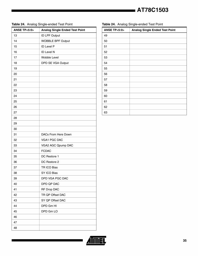
AT78C1503
13 ID LPF Output
14 WOBBLE BPF Output
15 ID Level P
16 ID Level N
17 Wobble Level
18 DPD SE VGA Output
19
20
21
22
23
24
25
26
27
28
29
30
31 DACs From Here Down
32 VGA1 PGC DAC
33 VGA2 AGC Qpump DAC
34 FCDAC
35 DC Restore 1
36 DC Restore 2
37 TR ICO Bias
38 SY ICO Bias
39 DPD VGA PGC DAC
40 DPD QP DAC
41 RF Drop DAC
42 TR QP Offset DAC
43 SY QP Offset DAC
44 DPD Gm HI
45 DPD Gm LO
46
47
48
Table 24. Analog Single-ended Test Point
ANSE TP<5:0> Analog Single Ended Test Point
49
50
51
52
53
54
55
56
57
58
59
60
61
62
63
Table 24. Analog Single-ended Test Point
ANSE TP<5:0> Analog Single Ended Test Point
35
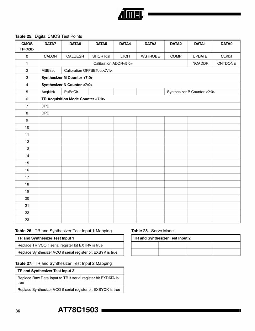
Table 25. Digital CMOS Test Points
CMOSTP<4:0>
DATA7 DATA6 DATA5 DATA4 DATA3 DATA2 DATA1 DATA0
0 CALON CALUESR SHORTcal LTCH WSTROBE COMP UPDATE CLKbit
1 Calibration ADDR<5:0> INCADDR CNTDONE
2 MSBset Calibration OFFSETout<7:1>
3 Synthesizer M Counter <7:0>
4 Synthesizer N Counter <7:0>
5 AcqNtrk PuPdClr Synthesizer P Counter <2:0>
6 TR Acquisition Mode Counter <7:0>
7 DPD
8 DPD
9
10
11
12
13
14
15
16
17
18
19
20
21
22
23
Table 26. TR and Synthesizer Test Input 1 Mapping
TR and Synthesizer Test Input 1
Replace TR VCO if serial register bit EXTRV is true
Replace Synthesizer VCO if serial register bit EXSYV is true
Table 27. TR and Synthesizer Test Input 2 Mapping
TR and Synthesizer Test Input 2
Replace Raw Data Input to TR if serial register bit EXDATA is true
Replace Synthesizer VCO if serial register bit EXSYCK is true
Table 28. Servo Mode
TR and Synthesizer Test Input 2
AT78C150336
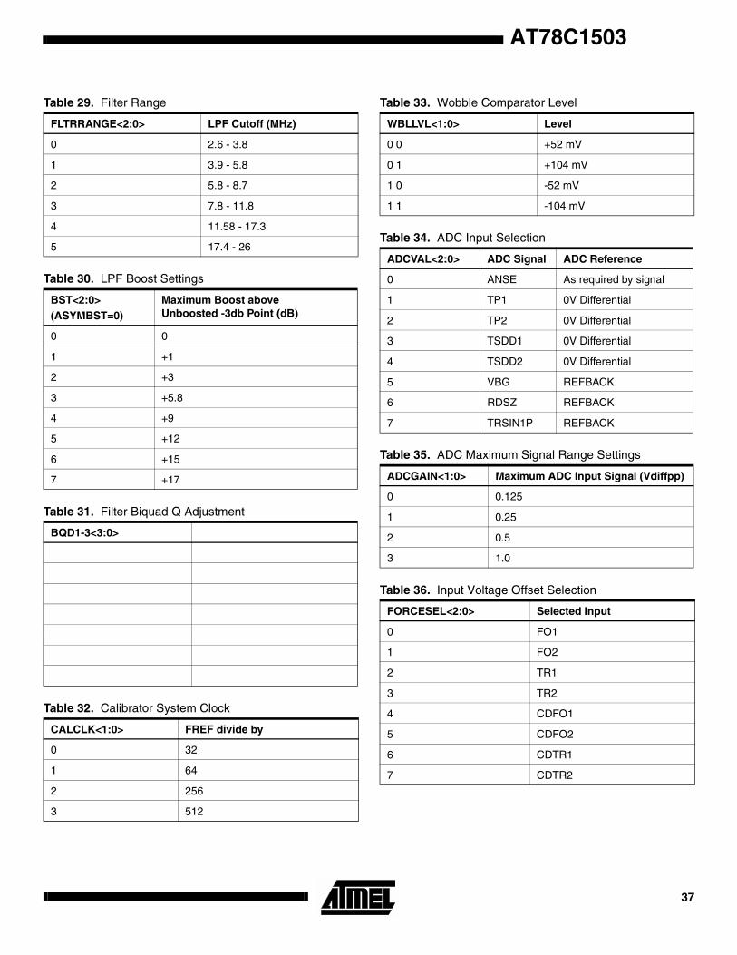
AT78C1503
Table 29. Filter Range
FLTRRANGE<2:0> LPF Cutoff (MHz)
0 2.6 - 3.8
1 3.9 - 5.8
2 5.8 - 8.7
3 7.8 - 11.8
4 11.58 - 17.3
5 17.4 - 26
Table 30. LPF Boost Settings
BST<2:0>(ASYMBST=0)
Maximum Boost above Unboosted -3db Point (dB)
0 0
1 +1
2 +3
3 +5.8
4 +9
5 +12
6 +15
7 +17
Table 31. Filter Biquad Q Adjustment
BQD1-3<3:0>
Table 32. Calibrator System Clock
CALCLK<1:0> FREF divide by
0 32
1 64
2 256
3 512
Table 33. Wobble Comparator Level
WBLLVL<1:0> Level
0 0 +52 mV
0 1 +104 mV
1 0 -52 mV
1 1 -104 mV
Table 34. ADC Input Selection
ADCVAL<2:0> ADC Signal ADC Reference
0 ANSE As required by signal
1 TP1 0V Differential
2 TP2 0V Differential
3 TSDD1 0V Differential
4 TSDD2 0V Differential
5 VBG REFBACK
6 RDSZ REFBACK
7 TRSIN1P REFBACK
Table 35. ADC Maximum Signal Range Settings
ADCGAIN<1:0> Maximum ADC Input Signal (Vdiffpp)
0 0.125
1 0.25
2 0.5
3 1.0
Table 36. Input Voltage Offset Selection
FORCESEL<2:0> Selected Input
0 FO1
1 FO2
2 TR1
3 TR2
4 CDFO1
5 CDFO2
6 CDTR1
7 CDTR2
37
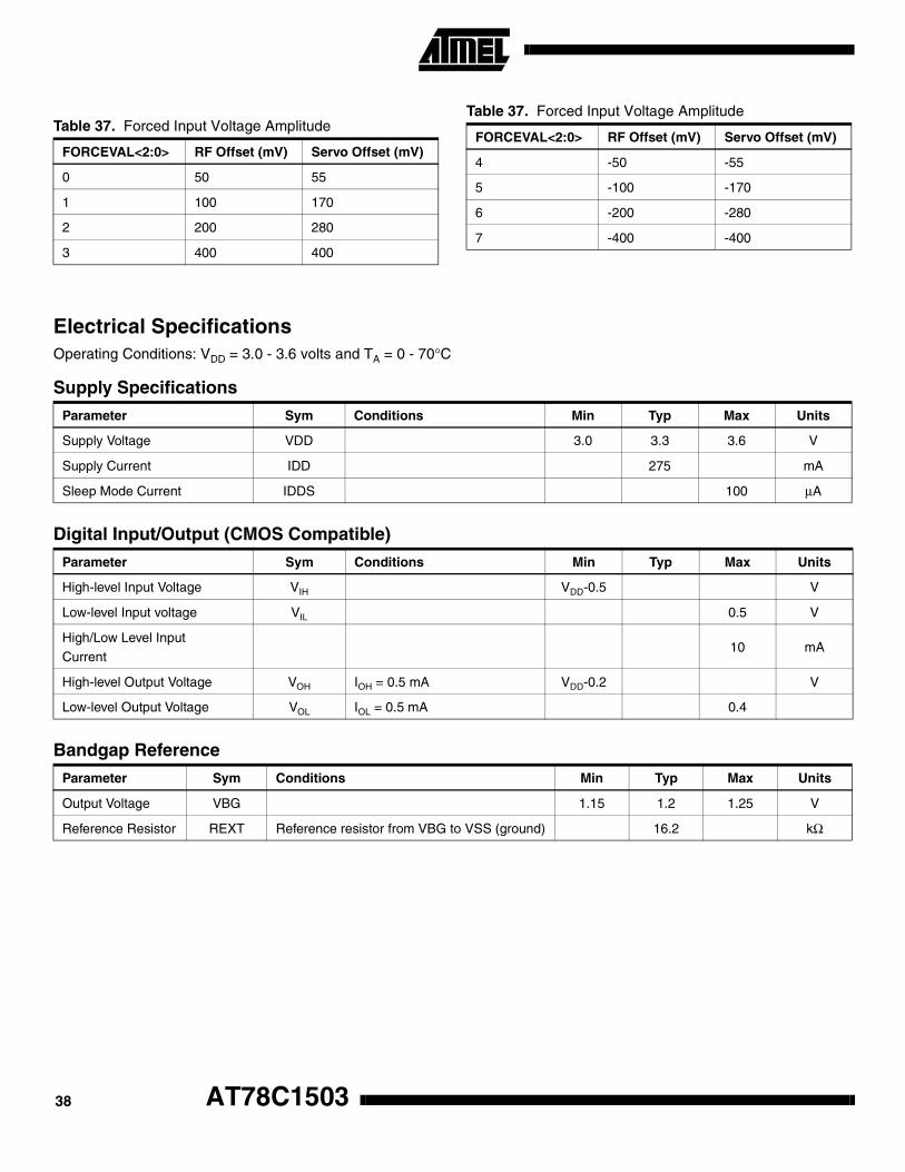
Electrical SpecificationsOperating Conditions: VDD = 3.0 - 3.6 volts and TA = 0 - 70°C
Table 37. Forced Input Voltage Amplitude
FORCEVAL<2:0> RF Offset (mV) Servo Offset (mV)
0 50 55
1 100 170
2 200 280
3 400 400
4 -50 -55
5 -100 -170
6 -200 -280
7 -400 -400
Table 37. Forced Input Voltage Amplitude
FORCEVAL<2:0> RF Offset (mV) Servo Offset (mV)
Supply Specifications
Parameter Sym Conditions Min Typ Max Units
Supply Voltage VDD 3.0 3.3 3.6 V
Supply Current IDD 275 mA
Sleep Mode Current IDDS 100 µA
Digital Input/Output (CMOS Compatible)
Parameter Sym Conditions Min Typ Max Units
High-level Input Voltage VIH VDD-0.5 V
Low-level Input voltage VIL 0.5 V
High/Low Level InputCurrent
10 mA
High-level Output Voltage VOH IOH = 0.5 mA VDD-0.2 V
Low-level Output Voltage VOL IOL = 0.5 mA 0.4
Bandgap Reference
Parameter Sym Conditions Min Typ Max Units
Output Voltage VBG 1.15 1.2 1.25 V
Reference Resistor REXT Reference resistor from VBG to VSS (ground) 16.2 kΩ
AT78C150338
AT78C1503
Variable Gain Amplifier (VGA)
Parameter Sym Conditions Min Typ Max Units
Gain Range 1 10 V/V
Input Dynamic Range
(Low-mode)DRL 30 300 mV
Input Dynamic Range
(High-mode)DRH 60 600 mV
Bandwidth AGCBW -3dB 100 MHz
AGC Control Sensitivity AGC mode 20 dB/V
AGC Locking Voltage(Input to data slicer)
VAGCPeak-to-peak differential input to slicer in AGC mode
1 V
Total Harmonic Distortion THDMeasured at the detector input. 750 mVppd lock in AGC mode
2 %
Common Mode Rejection Ratio CMRR Vin = 250 mV common mode @10 MHz 40 dB
Power Supply Rejection Ratio PSRR Vsup = 250 mV @10 MHz 40 dB
7th Order Equiripple Filter/Equalizer
Parameter Sym Conditions Min Typ Max Units
Filter Cutoff Frequency Programmability
Fc 4.4 22 MHz
Filter Boost Range FbMeasured from lowfrequency gain
0 13 dB
Cutoff frequencyAccuracy
All frequency ranges -10 +10 %
Boost Accuracy All frequency ranges -2 +2 dB
Group Delay Variation All frequency ranges -4 +4 %
Data Phase Locked Loop
Parameter Sym Conditions Min Typ Max Units
Frequency Supported 26 146 MHz
RMS Jitter TBD degrees
Pull-in Range -2.5 +2.5 % of Fc
Frequency Synthesizer
Parameter Sym Conditions Min Typ Max Units
Frequency Supported 26 146 MHz
External Source 15 40 MHz
39
Serial Register
Parameter Sym Conditions Min Typ Max Units
Serial Clock Frequency SCLK 0.01 20 MHz
SENA to SCLKSet-up Time
TEC Transition time serial enable to serial clock 10 ns
SCLK Pulse Width TPW 20 ns
SCLK to SDATAHold Time
THCD 10 ns
SDATA to SCLKSet-up Time
TSDC 10 ns
Table 38. Pin List
Pin # Pin Name Type Description
1 IDFIELD Output Signal to preamp to drive ID select
2 RFP Analog Input High-speed signal input
3 RFN Analog Input High-speed signal input
4 FO1P Differential Input Focus 1 Positive
5 FO1N Differential Input Focus 1 Negative
6 FO2P Differential Input Focus 2 Positive
7 FO2N Differential Input Focus 2 Negative
8 TR1P Differential Input Track 1 Positive
9 TR1N Differential Input Track 1 Negative
10 TR2P Differential Input Track 2 Positive
11 TR2N Differential Input Track 2 Negative
12 FOHG
13 REXT Passive Passive for 0 TC current reference
14 VDD1 +3.3V Supply DPD, IBIAS
15 VSS1 0 V Supply DPD, IBIAS
16 FO1_CD Analog Input Focus 1, CD Input
17 FO2_CD Analog Input Focus 2, CD Input
18 TR1_CD Analog Input Track 1, CD Input
19 TR2_CD Analog Input Track 2, CD Input
20 VDD6 +3.3V Supply Slow Servo Analog
21 SS_H
22 VSS6 0V Supply Slow Servo Analog
23 REFFRONT Input/Output Servo Front-end reference level
24 REFBACK Input/Output Servo Back-end reference level
25 LENSPOS Analog Input Lens position error input
AT78C150340
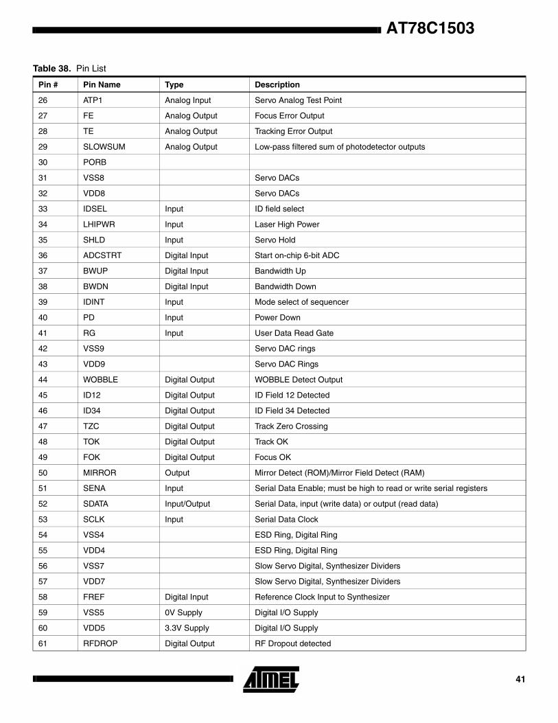
AT78C1503
26 ATP1 Analog Input Servo Analog Test Point
27 FE Analog Output Focus Error Output
28 TE Analog Output Tracking Error Output
29 SLOWSUM Analog Output Low-pass filtered sum of photodetector outputs
30 PORB
31 VSS8 Servo DACs
32 VDD8 Servo DACs
33 IDSEL Input ID field select
34 LHIPWR Input Laser High Power
35 SHLD Input Servo Hold
36 ADCSTRT Digital Input Start on-chip 6-bit ADC
37 BWUP Digital Input Bandwidth Up
38 BWDN Digital Input Bandwidth Down
39 IDINT Input Mode select of sequencer
40 PD Input Power Down
41 RG Input User Data Read Gate
42 VSS9 Servo DAC rings
43 VDD9 Servo DAC Rings
44 WOBBLE Digital Output WOBBLE Detect Output
45 ID12 Digital Output ID Field 12 Detected
46 ID34 Digital Output ID Field 34 Detected
47 TZC Digital Output Track Zero Crossing
48 TOK Digital Output Track OK
49 FOK Digital Output Focus OK
50 MIRROR Output Mirror Detect (ROM)/Mirror Field Detect (RAM)
51 SENA Input Serial Data Enable; must be high to read or write serial registers
52 SDATA Input/Output Serial Data, input (write data) or output (read data)
53 SCLK Input Serial Data Clock
54 VSS4 ESD Ring, Digital Ring
55 VDD4 ESD Ring, Digital Ring
56 VSS7 Slow Servo Digital, Synthesizer Dividers
57 VDD7 Slow Servo Digital, Synthesizer Dividers
58 FREF Digital Input Reference Clock Input to Synthesizer
59 VSS5 0V Supply Digital I/O Supply
60 VDD5 3.3V Supply Digital I/O Supply
61 RFDROP Digital Output RF Dropout detected
Table 38. Pin List
Pin # Pin Name Type Description
41

62 RCLK Digital Output Recovered clock divided by 4 or 8
63 DATA0 Output Recovered data out, Bit 0 (last in time)
64 DATA1 Output Recovered data out, Bit 1
65 DATA2 Output Recovered data out, Bit 2
66 DATA3 Output Recovered data out, Bit 3
67 DATA4 Output Recovered data out, Bit 4
68 DATA5 Output Recovered data out, Bit 5
69 DATA6 Output Recovered data out, Bit 6
70 DATA7 Output Recovered data out, Bit 7 (first in time)
71 VSS11 0V Supply Digital I/O Ring
72 VDD11 +3.3V Supply Digital I/O Ring
73 VSS3 0V Supply TR CML, Synthesizer CML, DC Restore
74 VDD3 +3.3V Supply TR CML, Synthesizer CML, DC Restore
75 TRCST Input Timing recovery coast
76 WCLK Output Write Clock
77 WG Input Write Gate (enables Write Clock)
78 TRSIN2N Differential Input Timing Recovery/Synthesizer test input
79 TRSIN2P Differential Input Timing Recovery/Synthesizer test input
80 TRSIN1N Differential Input Timing Recovery/Synthesizer test input
81 TRSIN1P Differential Input Timing Recovery/Synthesizer test input
82 TSDDTP1N Test Output TR/Detector/Phase Detector test point
83 TSDDTP1P Test Output TR/Detector/Phase Detector test point
84 TSDDTP2N Test Output TR/Detector/Phase Detector test point
85 TSDDTP2P Test Output TR/Detector/Phase Detector test point
86 CDCRN Analog Detector Duty Cycle Feedback Cap
87 CDCRP Analog Detector Duty Cycle Feedback Cap
88 VDD2 +3.3V Supply RF Frontend Ring
89 VSS2 0V Supply RF Frontend Ring
90 TP2N Differential Output Test Point 2 Output
91 TP2P Differential Output Test Point 2 Output
92 TP1N Differential Output Test Point 1 Output
93 TP1P Differential Output Test Point 1 Output
94 AGCHLD Digital Input AGC Hold Input
95 AGCFST Digital Input AGC Fast Recovery Input
96 VSS10 AGC, LPF
97 VDD10 AGC, LPF
Table 38. Pin List
Pin # Pin Name Type Description
AT78C150342
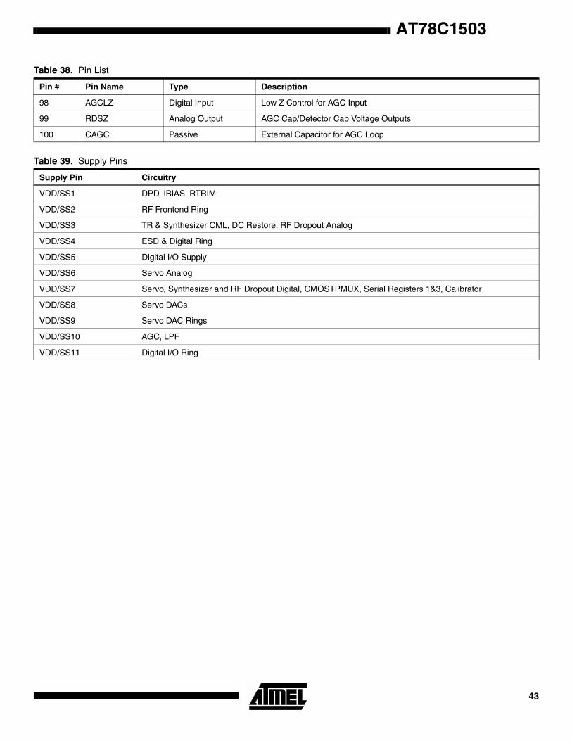
AT78C1503
98 AGCLZ Digital Input Low Z Control for AGC Input
99 RDSZ Analog Output AGC Cap/Detector Cap Voltage Outputs
100 CAGC Passive External Capacitor for AGC Loop
Table 38. Pin List
Pin # Pin Name Type Description
Table 39. Supply Pins
Supply Pin Circuitry
VDD/SS1 DPD, IBIAS, RTRIM
VDD/SS2 RF Frontend Ring
VDD/SS3 TR & Synthesizer CML, DC Restore, RF Dropout Analog
VDD/SS4 ESD & Digital Ring
VDD/SS5 Digital I/O Supply
VDD/SS6 Servo Analog
VDD/SS7 Servo, Synthesizer and RF Dropout Digital, CMOSTPMUX, Serial Registers 1&3, Calibrator
VDD/SS8 Servo DACs
VDD/SS9 Servo DAC Rings
VDD/SS10 AGC, LPF
VDD/SS11 Digital I/O Ring
43

Ordering InformationOrdering Code Package Operation Range
AT78C1503-100TC 100 Pin TQFP Commercial (0°C to 70°C)
AT78C1503-100LC 100 Pin LQFP Commercial (0°C to 70°C)
Package Type
100T 100-Lead, Thin Quad Flat Pack (TQFP)
100L 100-Lead, Low Quad Flat Pack (LQFP)
AT78C150344
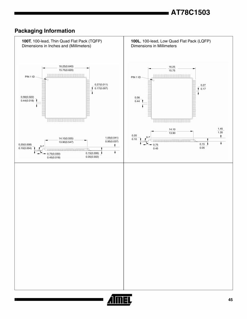
AT78C1503
Packaging Information
PIN 1 ID
0.56(0.022)0.44(0.018)
16.25(0.640)
15.75(0.620)
0.27(0.011)
0.17(0.007)
14.10(0.555)13.90(0.547)
0.15(0.006)0.05(0.002)
0.75(0.030)0.45(0.018)
0-70.20(0.008)0.10(0.004)
1.05(0.041)0.95(0.037)
PIN 1 ID
0.560.44
16.2515.75
0.27
0.17
14.1013.90
0.150.05
0.750.45
0-70.200.10
1.451.35
100T, 100-lead, Thin Quad Flat Pack (TQFP)Dimensions in Inches and (Millimeters)
100L, 100-lead, Low Quad Flat Pack (LQFP)Dimensions in Millimeters
45
© Atmel Corporation 2000.Atmel Corporation makes no warranty for the use of its products, other than those expressly contained in the Company’s standard war-ranty which is detailed in Atmel’s Terms and Conditions located on the Company’s web site. The Company assumes no responsibility forany errors which may appear in this document, reserves the right to change devices or specifications detailed herein at any time withoutnotice, and does not make any commitment to update the information contained herein. No licenses to patents or other intellectual prop-erty of Atmel are granted by the Company in connection with the sale of Atmel products, expressly or by implication. Atmel’s products arenot authorized for use as critical components in life support devices or systems.
Atmel Headquarters Atmel Operations
Corporate Headquarters2325 Orchard ParkwaySan Jose, CA 95131TEL (408) 441-0311FAX (408) 487-2600
EuropeAtmel U.K., Ltd.Coliseum Business CentreRiverside WayCamberley, Surrey GU15 3YLEnglandTEL (44) 1276-686-677FAX (44) 1276-686-697
AsiaAtmel Asia, Ltd.Room 1219Chinachem Golden Plaza77 Mody Road TsimhatsuiEast KowloonHong KongTEL (852) 2721-9778FAX (852) 2722-1369
JapanAtmel Japan K.K.9F, Tonetsu Shinkawa Bldg.1-24-8 ShinkawaChuo-ku, Tokyo 104-0033JapanTEL (81) 3-3523-3551FAX (81) 3-3523-7581
Atmel Colorado Springs1150 E. Cheyenne Mtn. Blvd.Colorado Springs, CO 80906TEL (719) 576-3300FAX (719) 540-1759
Atmel RoussetZone Industrielle13106 Rousset CedexFranceTEL (33) 4-4253-6000FAX (33) 4-4253-6001
Fax-on-DemandNorth America:1-(800) 292-8635
International:1-(408) 441-0732
Web Sitehttp://www.atmel.com
BBS1-(408) 436-4309
Printed on recycled paper.
1214C–03/00/xM
Marks bearing ® and/or ™ are registered trademarks and trademarks of Atmel Corporation.
Terms and product names in this document may be trademarks of others.