ata disk module 5s -...
TRANSCRIPT

RoHS Recast Compliant
ATA Disk Module 5S
ADM5S 40P/180D Specifications
November 26, 2015
Version 1.1
Apacer Technology Inc.
1F, No.32, Zhongcheng Rd., Tucheng Dist., New Taipei City, Taiwan, R.O.C
Tel: +886-2-2267-8000 Fax: +886-2-2267-2261
www.apacer.com

ADM5S AP-FMxxxxD560XS-XTXXX
1 © 2015 Apacer Technology Inc. Rev. 1.1
Features:
Standard ATA/IDE Bus Interface – ATA command set compatible – Compliant with ATA/ATAPI-8 – ATA operating mode supports up to:
PIO Mode up to 4 Multiword DMA Mode up to 2 Ultra DMA Mode up to 6
Capacity – 128, 256, 512 MB – 1, 2, 4, 8, 16, 32 GB
Performance* – Sustained read: Up to 75 MB/sec – Sustained write: Up to 65 MB/sec
Flash Management – Advanced Wear-leveling algorithms – Built-in Hardware ECC – Flash block management – Power Failure Management – S.M.A.R.T.
NAND Flash Type: SLC
MTBF > 1,000,000 hours
Temperature Ranges – Operation:
Standard : 0°C to 70°C Extended : -40°C to 85°C
– Storage: -40°C to 100°C
Connector Type – 40-pin female connector
Power Consumption * – Supply voltage: 3.3V / 5V – Active mode: 280 mA – Idle mode: 15 mA
Form Factor – ATA Disk Module – Without Housing
Dimensions: 50.93x25.95x6.00 (unit: ㎜)
– With Housing
Dimensions: 58.99x27.83x6.25 (unit: ㎜)
ATA Secure Erase
RoHS Recast Compliant (2011/65/EU)
Master/Slave Switch (optional)
Note: the values addressed for performance and power consumption are typical and may vary in real world applications due to various platform configurations.
ADM5S AP-FMxxxxD560XS-XTXXX
2 © 2015 Apacer Technology Inc. Rev. 1.1
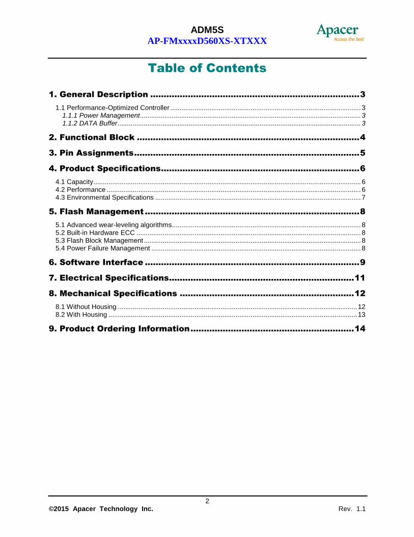
Table of Contents
1. General Description .............................................................................. 3
1.1 Performance-Optimized Controller ...................................................................................................... 3 1.1.1 Power Management ...................................................................................................................... 3 1.1.2 DATA Buffer .................................................................................................................................. 3
2. Functional Block ................................................................................... 4
3. Pin Assignments .................................................................................... 5
4. Product Specifications .......................................................................... 6
4.1 Capacity ............................................................................................................................................... 6 4.2 Performance ........................................................................................................................................ 6 4.3 Environmental Specifications .............................................................................................................. 7
5. Flash Management ................................................................................ 8
5.1 Advanced wear-leveling algorithms ..................................................................................................... 8 5.2 Built-in Hardware ECC ........................................................................................................................ 8 5.3 Flash Block Management .................................................................................................................... 8 5.4 Power Failure Management ................................................................................................................ 8
6. Software Interface ................................................................................ 9
7. Electrical Specifications..................................................................... 11
8. Mechanical Specifications ................................................................. 12
8.1 Without Housing ................................................................................................................................ 12 8.2 With Housing ..................................................................................................................................... 13
9. Product Ordering Information ............................................................. 14

ADM5S AP-FMxxxxD560XS-XTXXX
3 © 2015 Apacer Technology Inc. Rev. 1.1
1. General Description
Apacer ATA Disk Module 5S (ADM5S) SSD delivers ultra smooth performance and extremely low power consumption. This device supports DMA mode up to UDMA 6 that offers advanced data transfer technology and internal memory efficiency, which effectively decreases the loading for the microprocessor. Compliant with ATA/ATAPI-8 standards, our ADM5S supports data transfer modes up to PIO 4, Multiword DMA 2, and Ultra DMA 6. Equipped with power Error Correction Coding (ECC) up to 72 bit/1KB, the ADM5S can provide high data integrity. Aside from data efficiency, the ADM5S also comes with power management. The device can work at 3.3V or 5V power supply, with the output voltage automatically adjusted by the voltage regulator in the core. In addition, the built-in ECC engine can support multi-mode correction capability up to 72 bits and perform effective decoding throughput with high reliability.
Well suited for embedded flash storage applications by offering new and expanded functionalities as well as more cost-effective designs, better performance and increased reliability, ADM is designed to work at either 5 or 3.3 Volts, and supports the standard ATA driver complying with all major operating systems such as Microsoft’s Windows series, Apple’s Mac OS family, and Unix variants. Featuring technologies as Advanced Wear-leveling algorithms, S.M.A.R.T, Intelligent Power Failure Recovery, and ATA Secure Erase, Apacer’s ADM assures users of a versatile device on data storage.
1.1 Performance-Optimized Controller
The heart of an ATA-Disk Module is the ATA controller, which translates standard ATA signals into the data and controls of the flash media. This proprietary ATA controller is specifically designed to attain high data throughput from the host to the flash.
1.1.1 Power Management
The controller unit of this ADM storage device is made for power efficiency. It comes with built-in 2.7V voltage detectors for power fail prevention. In addition, it also supports 1.2V power-on reset.
1.1.2 DATA Buffer
The ATA-Disk Module Controller is programmed with a 128KB data buffer to optimize the host’s data transfer to and from the flash media.

ADM5S AP-FMxxxxD560XS-XTXXX
4 © 2015 Apacer Technology Inc. Rev. 1.1
2. Functional Block
The ATA-Disk Module (ADM) includes the ATA controller and flash media, as well as the ATA standard interface. Figure 2-1 shows the functional block diagram.
Figure 2-1: Functional block diagram

ADM5S AP-FMxxxxD560XS-XTXXX
5 © 2015 Apacer Technology Inc. Rev. 1.1
3. Pin Assignments
Table 3-1 lists the pin assignments with respective signal names for the 40-pin configuration. A “#” suffix indicates the active low signal. The pin type can be input, output or input/output.
Table 3-1: Pin assignments for the 40-pin configuration
Pin No. Signal Name Pin Type I/O Type Pin No. Signal Name Pin Type I/O Type
1 RESET# I I2U 2 GND - Ground
3 D7 I/O I1Z, O2 4 D8 I/O I1Z, O2
5 D6 I/O I1Z, O2 6 D9 I/O I1Z, O2
7 D5 I/O I1Z, O2 8 D10 I/O I1Z, O2
9 D4 I/O I1Z, O2 10 D11 I/O I1Z, O2
11 D3 I/O I1Z, O2 12 D12 I/O I1Z, O2
13 D2 I/O I1Z, O2 14 D13 I/O I1Z, O2
15 D1 I/O I1Z, O2 16 D14 I/O I1Z, O2
17 D0 I/O I1Z, O2 18 D15 I/O I1Z, O2
19 GND - Ground 20 NC - Power
21 DMARQ O O1 22 GND Ground
23 IOWR#
STOP I I2Z 24 GND - Ground
25
IORD#
HDMARDY#
HSTROBE#
I I2Z 26 GND - Ground
27
IORDY
DDMARDY#
DSTROBE
O O1 28 CSEL I I1U
29 DMACK# I I2U- 30 NC/WP#* -/I -/I1U
31 INTRQ O O1 32 IOCS16# O O2
33 A1 I I1Z 34 PDIAG# I/O I1U, O1
35 A0 I I1Z 36 A2 I I1Z
37 CS1FX# I I2Z 38 CS3FX# I I2Z
39 DASP# I/O I1U, O6 40 GND - Ground *Pin 30 is selectable as NC or WP# through a zero ohm resistor jumper. Default is NC. Note that pin 30 is a GND pin on standard ATA interface. This pin could be redesigned for host to control the write protect function on ADM

ADM5S AP-FMxxxxD560XS-XTXXX
6 © 2015 Apacer Technology Inc. Rev. 1.1
4. Product Specifications
4.1 Capacity
Capacity specification of the ATA-Disk Module (ADM) product family is available as shown in Table 4-1.
Table 4-1: Capacity specifications (unformatted)
Capacity Total bytes Cylinders Heads Sectors Max LBA
128 MB 128,057,344 977 8 32 250,112
256 MB 256,901,120 980 16 32 501,760
512 MB 512,483,368 993 16 63 1,000,944
1 GB 1,011,032,064 1,959 16 63 1,974,672
2 GB 2,011,226,112 3,897 16 63 3,928,176
4 GB 4,011,614,208 7,773 16 63 7,835,184
8 GB 8,012,390,400 15,525 16 63 15,649,200
16 GB 16,013,942,784 16,383 16 63 31,277,232
32 GB 32,017,047,552 16,383 16 63 62,533,296 *Cylinders, heads or sectors are not applicable for these capacities. Only LBA addressing applies **Notes: 1 GB = 1,000,000,000 bytes; 1 sector = 512 bytes. LBA count addressed in the table above indicates total user storage capacity and will remain the same throughout the lifespan of the device. However, the total usable capacity of the SSD is most likely to be less than the total physical capacity because a small portion of the capacity is reserved for device maintenance usages.
4.2 Performance
Performances* of the ATA-Disk Module are listed in below tables.
Table 4-2: Performance specifications
Capacity
Performance 128 MB 256 GB 512 MB 1 GB 2 GB 4 GB 8 GB 16 GB 32 GB
Sustained read (MB/s)
20 20 30 30 55 35 70 75 75
Sustained write (MB/s)
11 11 20 20 40 30 60 65 65
*Results may differ from various flash configurations and platforms.

ADM5S AP-FMxxxxD560XS-XTXXX
7 © 2015 Apacer Technology Inc. Rev. 1.1
4.3 Environmental Specifications
Environmental specification of the ATA-Disk Module (ADM) follows the MIL-STD-810F standard.
Table 4-3: Environmental specifications
Environment Specifications
Temperature Operation 0°C to 70°C(Standard); -40°C to 85°C(Extended);
Storage -40°C to 100°C
Vibration (Non-Operating) Sine wave: 10~2000Hz, 15G (X, Y, Z axes)
Shock (Non-Operating) Half sine wave, 1500 G, 11 ms (X, Y, Z ; All 6 axes)

ADM5S AP-FMxxxxD560XS-XTXXX
8 © 2015 Apacer Technology Inc. Rev. 1.1
5. Flash Management
5.1 Advanced wear-leveling algorithms
Flash memory devices differ from Hard Disk Drives (HDDs) in terms of how blocks are utilized. For HDDs, when a change is made to stored data, like erase or update, the controller mechanism on HDDs will perform overwrites on blocks. Unlike HDDs, flash blocks cannot be overwritten and each P/E cycle wears down the lifespan of blocks gradually. Repeatedly program/erase cycles performed on the same memory cells will eventually cause some blocks to age faster than others. This would bring flash storages to their end of service term sooner. Wear leveling is an important mechanism that level out the wearing of blocks so that the wearing-down of blocks can be almost evenly distributed. This will increase the lifespan of SSDs. Commonly used wear leveling types are Static and Dynamic.
5.2 Built-in Hardware ECC
The properties of NAND flash memory make it ideal for applications that require high integrity while operating in challenging environments. The integrity of data to NAND flash memory is generally maintained through ECC algorithms. This ATA-Flash Drive is programmed with a hardware ECC engine which correct up to 72 bits per 1KB.
5.3 Flash Block Management
Current production technology is unable to guarantee total reliability of NAND flash memory array. When a flash memory device leaves factory, it comes with a minimal number of initial bad blocks during production or out-of-factory as there is no currently known technology that produce flash chips free of bad blocks. In addition, bad blocks may develop during program/erase cycles. When host performs program/erase command on a block, bad block may appear in Status Register. Since bad blocks are inevitable, the solution is to keep them in control. Apacer flash devices are programmed with ECC, block mapping technique and S.M.A.R.T to reduce invalidity or error. Once bad blocks are detected, data in those blocks will be transferred to free blocks and error will be corrected by designated algorithms.
5.4 Power Failure Management
Power Failure Management plays a crucial role when experiencing unstable power supply. Power disruption may occur when users are storing data into the SSD. In this urgent situation, the controller would run multiple write-to-flash cycles to store the metadata for later block rebuilding. This urgent operation requires about several milliseconds to get it done. At the next power up, the firmware will perform a status tracking to retrieve the mapping table and resume previously programmed NAND blocks to check if there is any incompleteness of transmission.
5.5 Mean Time Between Failures (MTBF)
Mean Time Between Failures (MTBF) is predicted based on reliability data for the individual components in the drive. The prediction result for the drive is more than 1,000,000 hours.
Notes about the MTBF:
The MTBF is predicated and calculated based on “Telcordia Technologies Special Report, SR-332, Issue 2” method.

ADM5S AP-FMxxxxD560XS-XTXXX
9 © 2015 Apacer Technology Inc. Rev. 1.1
6. Software Interface
6.1 Command Set
This section defines the software requirements and the format of the commands the host sends to the ATA-Disk Module (ADM). Commands are issued to the ADM by loading the required registers in the command block with the supplied parameters, and then writing the command code to the Command register. The manner in which a command is accepted varies.
Table 6-1: Command set (1 of 2)
Command Code
Check-Power-Mode E5H or 98H
Execute-Drive-Diagnostic 90H
Erase Sector(s) C0H
Flush-Cache E7H
Format Track 50H
Identify-Drive ECH
Idle E3H or 97H
Idle-Immediate E1H or 95H
Initialize-Drive-Parameters 91H
NOP 00H
Read-Buffer E4H
Read-DMA C8H or C9H
Read-Multiple C4H
Read-Sector(s) 20H or 21H
Read-Verify-Sector(s) 40H or 41H
Recalibrate 1XH
Request-Sense 03H
Security-Disable-Password F6H
Security-Erase-Prepare F3H
Security-Erase-Unit F4H
Security-Freeze-Lock F5H
Security-Set-Password F1H
Security-Unlock F2H
Seek 7XH
Set-Features EFH

ADM5S AP-FMxxxxD560XS-XTXXX
10 © 2015 Apacer Technology Inc. Rev. 1.1
Table 6-1: Command set (2 of 2)
Command Code
SMART B0H
Set-Multiple-Mode C6H
Set-Sleep-Mode E6H or 99H
Standby E2H or 96H
Standby-lmmediate E0H or 94H
Translate-Sector 87H
Write-Buffer E8H
Write-DMA CAH or CBH
Write-Multiple C5H
Write-Multiple-Without-Erase CDH
Write-Sector(s) 30H or 31H
Write-Sector-Without-Erase 38H
Write-Verify 3CH
6.2 S.M.A.R.T.
S.M.A.R.T. is an acronym for Self-Monitoring, Analysis and Reporting Technology, an open standard allowing disk drives to automatically monitor their own health and report potential problems. It protects the user from unscheduled downtime by monitoring and storing critical drive performance and attributes parameters. Ideally, this should allow taking proactive actions to prevent impending drive failure.
Apacer devices use the standard SMART command B0h to read data out from the drive to activate our SMART feature that complies with the ATA/ATAPI-7 specifications. Based on the SFF-8035i Rev. 2.0 specifications, SMART Attribute IDs shall include Initial bad block count, Bad block count, Spare block count, Maximum erase count, Average erase count and Power cycle. When the SMART Utility running on the host, it analyzes and reports the disk status to the host before the device reaches in critical condition.
6.3. ATA Secure Erase
ATA Secure Erase is an ATA disk purging command currently embedded in most of the storage drives. Defined in ATA specifications, (ATA) Secure Erase is part of Security Feature Set that allows storage drives to erase all user data areas. The erase process usually runs on the firmware level as most of the ATA-based storage media currently in the market are built-in with this command. ATA Secure Erase can securely wipe out the user data in the drive and protects it from malicious attack.

ADM5S AP-FMxxxxD560XS-XTXXX
11 © 2015 Apacer Technology Inc. Rev. 1.1
7. Electrical Specifications
Table 7-1: Operating range
Operating voltage 3.135-3.465V
4.75-5.25V
Table 7-2: Power consumptions (typical)
Capacity
Modes 128 MB 256 MB 512 MB 1 GB 2 GB 4 GB 8 GB 16 GB 32 GB
Active (mA) 125 125 135 135 195 160 230 250 280
Idle (mA) 15 15 15 15 15 15 15 15 15
*Results were tested at 5.0V power supply and may differ from various flash configurations and platforms.

ADM5S AP-FMxxxxD560XS-XTXXX
12 © 2015 Apacer Technology Inc. Rev. 1.1
8. Mechanical Specifications
8.1 Without Housing
Unit: ㎜
Tolerance: ±0.2 ㎜

ADM5S AP-FMxxxxD560XS-XTXXX
13 © 2015 Apacer Technology Inc. Rev. 1.1
8.2 With Housing
Unit: ㎜
Tolerance: ±0.2 ㎜

ADM5S AP-FMxxxxD560XS-XTXXX
14 © 2015 Apacer Technology Inc. Rev. 1.1
9. Product Ordering Information
9.1 Product Code Designations
A P – FM xxxx D 5 6 0 X S – X T X XX
Apacer Product Code
Model Name
Capacity: 0128: 128MB 001G: 1GB 008G: 8GB 0256: 256MB 002G: 2GB 016G: 16GB 0512: 512MB 004G: 4GB 032G: 32GB
Controller Version
Package Modifier:
40 pin / 180D
PCB Version
Speed: 0: Standard
Voltage: 3: 3.3V 5: 5.0V
Environmental Spec
FW Version: Blank: Std.
Flash Type
Temperature: Blank: Standard
W: Wide Temp.
Model:
1M: Middle Profile Type 1H: Middle Profile with Housing
ADM5S AP-FMxxxxD560XS-XTXXX
15 © 2015 Apacer Technology Inc. Rev. 1.1
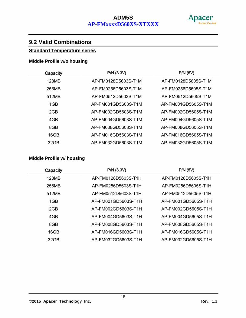
9.2 Valid Combinations
Standard Temperature series Middle Profile w/o housing
Capacity P/N (3.3V) P/N (5V)
128MB AP-FM0128D5603S-T1M AP-FM0128D5605S-T1M
256MB AP-FM0256D5603S-T1M AP-FM0256D5605S-T1M
512MB AP-FM0512D5603S-T1M AP-FM0512D5605S-T1M
1GB AP-FM001GD5603S-T1M AP-FM001GD5605S-T1M
2GB AP-FM002GD5603S-T1M AP-FM002GD5605S-T1M
4GB AP-FM004GD5603S-T1M AP-FM004GD5605S-T1M
8GB AP-FM008GD5603S-T1M AP-FM008GD5605S-T1M
16GB AP-FM016GD5603S-T1M AP-FM016GD5605S-T1M
32GB AP-FM032GD5603S-T1M AP-FM032GD5605S-T1M
Middle Profile w/ housing
Capacity P/N (3.3V) P/N (5V)
128MB AP-FM0128D5603S-T1H AP-FM0128D5605S-T1H
256MB AP-FM0256D5603S-T1H AP-FM0256D5605S-T1H
512MB AP-FM0512D5603S-T1H AP-FM0512D5605S-T1H
1GB AP-FM001GD5603S-T1H AP-FM001GD5605S-T1H
2GB AP-FM002GD5603S-T1H AP-FM002GD5605S-T1H
4GB AP-FM004GD5603S-T1H AP-FM004GD5605S-T1H
8GB AP-FM008GD5603S-T1H AP-FM008GD5605S-T1H
16GB AP-FM016GD5603S-T1H AP-FM016GD5605S-T1H
32GB AP-FM032GD5603S-T1H AP-FM032GD5605S-T1H

ADM5S AP-FMxxxxD560XS-XTXXX
16 © 2015 Apacer Technology Inc. Rev. 1.1
Extended Temperature series
Middle Profile w/o housing
Capacity P/N (3.3V) P/N (5V)
128MB AP-FM0128D5603S-TW1M AP-FM0128D5605S-TW1M
256MB AP-FM0256D5603S-TW1M AP-FM0256D5605S-TW1M
512MB AP-FM0512D5603S-TW1M AP-FM0512D5605S-TW1M
1GB AP-FM001GD5603S-TW1M AP-FM001GD5605S-TW1M
2GB AP-FM002GD5603S-TW1M AP-FM002GD5605S-TW1M
4GB AP-FM004GD5603S-TW1M AP-FM004GD5605S-TW1M
8GB AP-FM008GD5603S-TW1M AP-FM008GD5605S-TW1M
16GB AP-FM016GD5603S-TW1M AP-FM016GD5605S-TW1M
32GB AP-FM032GD5603S-TW1M AP-FM032GD5605S-TW1M
Middle Profile w/ housing
Capacity P/N (3.3V) P/N (5V)
128MB AP-FM0128D5603S-TW1H AP-FM0128D5605S-TW1H
256MB AP-FM0256D5603S-TW1H AP-FM0256D5605S-TW1H
512MB AP-FM0512D5603S-TW1H AP-FM0512D5605S-TW1H
1GB AP-FM001GD5603S-TW1H AP-FM001GD5605S-TW1H
2GB AP-FM002GD5603S-TW1H AP-FM002GD5605S-TW1H
4GB AP-FM004GD5603S-TW1H AP-FM004GD5605S-TW1H
8GB AP-FM008GD5603S-TW1H AP-FM008GD5605S-TW1H
16GB AP-FM016GD5603S-TW1H AP-FM016GD5605S-TW1H
32GB AP-FM032GD5603S-TW1H AP-FM032GD5605S-TW1H
ADM5S AP-FMxxxxD560XS-XTXXX
17 © 2015 Apacer Technology Inc. Rev. 1.1
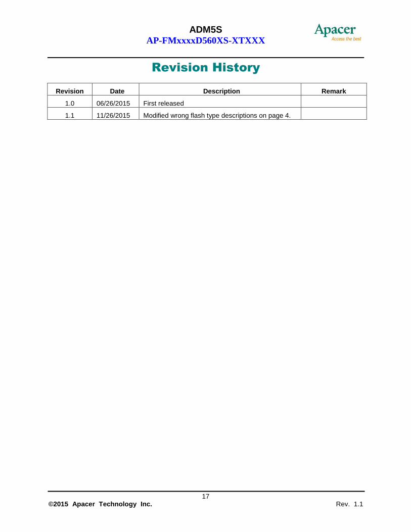
Revision History
Revision Date Description Remark
1.0 06/26/2015 First released
1.1 11/26/2015 Modified wrong flash type descriptions on page 4.

ADM5S AP-FMxxxxD560XS-XTXXX
18 © 2015 Apacer Technology Inc. Rev. 1.1
Global Presence
Taiwan (Headquarters)
Apacer Technology Inc.
1F., No.32, Zhongcheng Rd., Tucheng Dist., New Taipei City 236, Taiwan R.O.C. Tel: 886-2-2267-8000 Fax: 886-2-2267-2261 [email protected]
U.S.A.
Apacer Memory America, Inc.
46732 Lakeview Blvd., Fremont, CA 94538 Tel: 1-408-518-8699 Fax: 1-510-249-9568 [email protected]
Japan
Apacer Technology Corp.
5F, Matsura Bldg., Shiba, Minato-Ku Tokyo, 105-0014, Japan Tel: 81-3-5419-2668 Fax: 81-3-5419-0018 [email protected]
Europe
Apacer Technology B.V.
Science Park Eindhoven 5051 5692 EB Son, The Netherlands Tel: 31-40-267-0000 Fax: 31-40-267-0000#6199 [email protected]
China
Apacer Electronic (Shanghai) Co., Ltd
Room D, 22/FL, No.2, Lane 600, JieyunPlaza, Tianshan RD, Shanghai, 200051, China Tel: 86-21-6228-9939 Fax: 86-21-6228-9936 [email protected]
India
Apacer Technologies Pvt Ltd,
Unit No.201, “Brigade Corner”, 7th
Block Jayanagar, Yediyur Circle, Bangalore – 560082, India Tel: 91-80-4152-9061 Fax: 91-80-4170-0215 [email protected]