ata6670 - ww1.microchip.comww1.microchip.com/downloads/en/devicedoc/atmel-9204-lin-networ… ·...
TRANSCRIPT

ATA6670
Dual LIN Transceiver
DATASHEET
Features
● Operating range from 5V to 27V
● Baud rate up to 20Kbaud
● LIN physical layer according to LIN specification 2.0, 2.1 and SAEJ2602-2
● Fully compatible with 3.3V and 5V devices
● TXD dominant timeout timer
● Normal and sleep mode
● Wake-up capability via LIN bus (90µs dominant)
● Very low standby current during sleep mode (10µA)
● Bus pin is overtemperature and short-circuit protected versus GND and battery
● LIN input current < 2µA if VBAT Is disconnected
● Overtemperature protection
● High EMC level
● Interference and damage protection according to ISO/CD 7637
● Fulfills the OEM hardware requirements for LIN in automotive applications rev. 1.1
● Transceiver 2: additional INH high side switch output and high voltage WAKE input
● Qualified according to AEC-Q100
● Package: DFN14 with wettable flanks (Moisture Sensitivity Level 1)
Description
The Atmel® ATA6670 is a fully integrated dual-LIN transceiver complying with the LIN specification 2.0, 2.1, and SAEJ2602-2. There are two completely independent and sepa-rated LIN transceivers integrated in one package (only the GND pins GND1 and GND2 are internally connected). Each of them interfaces with the LIN protocol handler and the physi-cal layer.
The two LIN transceivers are nearly identical, the only difference is an additional WAKE input and an INH output at transceiver 2.
The device is designed to handle the low-speed data communication in vehicles, for exam-ple, in convenience electronics. Improved slope control at the LIN driver ensures secure data communication up to 20Kbaud. Sleep mode guarantees minimal current consumption for each transceiver even in the case of a floating bus line or a short-circuit on the LIN bus to GND. The Atmel ATA6670 features advanced EMI and ESD performance.
9204H-AUTO-10/14

Figure 1. Block Diagram
Receiver
+
-
Wake up bustimer
Slew rate control
Control unit
Filter
Short circuitand over-temperatureprotectionTXD
Time-OutTimer
Sleep mode
Receiver4RXD2
1RXD1
TXD2
GND2WAKE2
EN2
7
Transceiver 2
Transceiver 1
VS
VS
+
-
Wake up bustimer
Slew rate control
Control unit
Filter
Short circuitand over-temperatureprotectionTXD
Time-OutTimer
Wake-upTimer
Sleep mode
TXD13
EN12
6 8
5
GND112
LIN29
LIN113
VS210
VS114
INH2
11
ATA6670 [DATASHEET]9204H–AUTO–10/14
2

1. Pin Configuration
Figure 1-1. Pinning DFN14
Table 1-1. Pin Description
Pin Symbol Function
1 RXD1 Receives data output 1 (open drain)
2 EN1 Enables normal mode 1. When the input is open or low, transceiver 1 is in sleep mode.
3 TXD1 Transmits data input 1
4 RXD2 Receives data output 2 (open drain)
5 EN2 Enables normal mode 2. When the input is open or low, transceiver 2 is in sleep mode.
6 WAKE2 High voltage input for local wake-up request. If not needed, connect directly to VS2
7 TXD2Transmits data input 2. Active low output (strong pull-down) after a local wake-up request at transceiver 2.
8 GND2 Ground 2
9 LIN2 LIN bus line 2 input/output
10 VS2 Battery supply 2
11 INH2 VS2- related high-side switch output for controlling an external load, such as a voltage divider
12 GND1 Ground 1
13 LIN1 LIN bus line 1 input/output
14 VS1 Battery supply 1
RXD1
EN1
TXD1
RXD2
EN2
WAKE2
TXD2
VS1
LIN1
GND1
INH2
VS2
AtmelATA6670
LIN2
GND2
3ATA6670 [DATASHEET]9204H–AUTO–10/14

2. Functional Description
The functions described in the following text apply to each LIN transceiver. Therefore, if pin LIN is stated, this applies to each of the two receivers (LIN1 and LIN2), which work completely independently. The only internal connection is between GND1 and GND2. The functions only available at transceiver 2 are marked accordingly.
2.1 Physical Layer Compatibility
Since the LIN physical layer is independent of higher LIN layers (e.g., the LIN protocol layer), all nodes with a LIN physical layer according to revision 2.x can be mixed with LIN physical layer nodes, which are based on older versions (i.e., LIN 1.0, LIN 1.1, LIN 1.2, LIN 1.3) without any restrictions.
2.2 Supply Pin (VS)
Undervoltage detection is implemented to disable transmission if VS falls to a value below 5V in order to avoid false bus messages. After switching on VS, the corresponding transceiver switches to Fail-safe mode. The supply current for each transceiver in sleep mode is typically 10µA.
2.3 Ground Pin (GND)
The Atmel® ATA6670 does not affect the LIN bus in case of GND disconnection. It is able to handle a ground shift up to 11.5% of VS.
2.4 Bus Pin (LIN)
A low-side driver with internal current limitation and thermal shutdown and an internal pull-up resistor are implemented as specified for LIN 2.x. The voltage range is from –27V to +40V. This pin exhibits no reverse current from the LIN bus to VS, even in case of a GND shift or VBatt disconnection. The LIN receiver thresholds are compatible with the LIN protocol specification. The fall time (from recessive to dominant) and the rise time (from dominant to recessive) are slope-controlled. The output has a self-adapting short-circuit limitation; in other words, during current limitation, the current decreases in proportion to an increase in chip temperature.
Note: The internal pull-up resistor is only active in normal and fail-safe mode.
2.5 Input/Output Pin (TXD)
In normal mode the TXD pin is the microcontroller interface to control the state of the LIN output. TXD must be at low level in order to have a low LIN bus. If TXD is high, the LIN output transistor is turned off and the bus is in recessive state. The TXD pin is compatible with both a 3.3V and 5V supply.
Only for the LIN transceiver 2: The TXD 2 pin is used in Fail-safe mode as an output in order to signal the wake-up source (see Section 2.14 “Wake- up Source Recognition (Only available at Transceiver 2)” on page 9). The TXD output is current limited to < 8mA.
2.6 TXD Dominant Time-out Function
The TXD input has an internal pull-down resistor. An internal timer prevents the bus line from being driven permanently in dominant state. If TXD is forced to low longer than tDOM > 70ms, the LIN pin is switched off (recessive mode). To reset this mode, switch TXD to high (> 10µs) before switching LIN to dominant again.
2.7 Output Pin (RXD)
This pin reports the state of the LIN bus to the microcontroller. LIN high (recessive) is reported by a high level at RXD, LIN low (dominant) is reported by a low voltage at RXD. The output is an open drain, therefore it is compatible with a 3.3V or 5V power supply. The AC characteristics are defined with a pull-up resistor of 5kΩ to 5V and a load capacitor of 20pF. The output is short current protected. In unpowered mode (VS = 0V) RXD is switched off. For ESD protection a zener diode is integrated with VZ = 6.1V.
ATA6670 [DATASHEET]9204H–AUTO–10/14
4

2.8 Enable Input Pin (EN)
This pin controls the operation mode of the LIN transceiver. If EN = 1, the LIN transceiver is in normal mode, with the transmission path from TXD to LIN and from LIN to RXD both active. At a falling edge on EN, while TXD is already set to high, the device is switched to Sleep mode and no transmission is possible. In sleep mode, the LIN bus pin is connected to VS with a weak pull-up current source. The device can transmit only after being woken up. During sleep mode the device is still supplied from the battery voltage. The supply current is typically 10µA. The pin EN provides a pull-down resistor in order to force the transceiver into sleep mode in case the pin is disconnected.
2.9 WAKE-up Input Pin (WAKE2, Only Available at Transceiver 2)
This pin is a high-voltage input used to wake up the transceiver 2 from sleep mode. It is usually connected to an external transistor or a switch to generate a local wake-up. A pull-up current source with typically –10µA is implemented as well as a debounce timer with a typical debounce time of 35µs.
Even if the WAKE2 pin is pulled to GND, it is possible to switch the transceiver 2 into sleep mode.
If a local wake-up is not needed in the application, pin WAKE2 can be connected directly to pin VS2.
2.10 INH Output Pin (INH2, only available at Transceiver 2)
This pin is used to control an external load or to switch the LIN master pull-up resistor on/off at pin LIN2. The inhibit pin provides an internal switch towards VS2 which is protected by temperature monitoring. If transceiver 2 is in normal or fail-safe mode, the inhibit high-side switch is turned on. When the transceiver 2 is in Sleep mode, the inhibit switch is turned off, thus disabling the connected external devices.
A wake-up event on LIN2 or at pin WAKE2 puts the transceiver 2 into fail-safe mode and as a result the INH2 switches to the VS2 level. After a system power-up (VS2 rises from zero), the pin INH2 switches automatically to the VS2 level.
2.11 Operation Modes1. Normal mode
This is the normal transmitting and receiving mode. All features are available.
2. Sleep modeIn this mode the transmission path is disabled and the device is in low power mode. Supply current from VBatt is typically 10µA. A wake-up signal (either from the LIN bus or the WAKE2 input) is detected and switches the corre-sponding transceiver to fail-safe mode. If EN then switches to high, Normal mode is activated. Input debounce timers at pin WAKE2 (tWAKE), LIN (tBUS) and EN (tsleep,tnom) prevent undesirable wake-up events due to automotive transients or EMI. The internal termination between pin LIN and pin VS is disabled. Only a weak pull-up current (typical 10µA) between pin LIN and pin VS is present. Sleep mode can be activated independently of the current level on pin LIN.
3. Fail-safe modeAt system power-up or after a wake-up event, the transceiver automatically switches to fail-safe mode. When VS2 exceeds 5V, the transceiver 2 switches the INH2 pin to the VS2 level. LIN communication is switched off. The microcontroller of the application then confirms normal mode by setting the EN pin to high.
5ATA6670 [DATASHEET]9204H–AUTO–10/14

Figure 2-1. Operating Modes
2.12 Remote Wake-up via Dominant Bus State
A voltage lower than the LIN pre-wake detection VLINL at pin LIN activates the internal LIN receiver and starts the wake-up detection timer.
A falling edge at pin LIN, followed by a dominant bus level VBUSdom maintained for a certain period of time (> tBUS) and a rising edge at pin LIN results in a remote wake-up request. The transceiver switches to Fail-safe mode, at transceiver 2 the INH2 output is activated (switches to VS2) and the internal termination resistor is switched on. The remote wake-up request is indicated by a low level at pin RXD to interrupt the microcontroller (see Figure 2-2).
Figure 2-2. LIN Wake-up Waveform Diagram
Table 2-1. Table of Modes
Operating Mode Transceiver RXD LIN
Fail-safe Off High, except after wake-up Recessive
Normal On LIN-depending TXD-depending
Sleep Off High-ohmic Recessive
a: Power-up (VS > 3V)b: VS < 5Vc: Bus wake-up event
(only Transceiver 2)d: Wake-up from wake switch
EN = 1and not b
c or d
b b
a
EN = 0
EN = 1
Fail-Safe Mode
Power-up
Communication: OFFRXD: see table of Modes
Transceiver 2: INH2 switch ON if VS2 > 5V
Sleep ModeCommunication: OFF
Transceiver 2: INH2 switch OFF
Normal ModeCommunication: ON
Transceiver 2: INH2 switch ONLocal wake-up event
Go to sleep command
LIN Bus
RXD
EN
High or floating
NormalMode
EN HighNode in sleep state
Low
Bus wake-up filtering time(tBUS)
ATA6670 [DATASHEET]9204H–AUTO–10/14
6
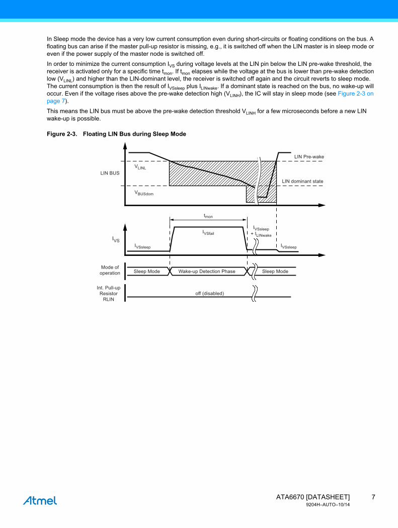
In Sleep mode the device has a very low current consumption even during short-circuits or floating conditions on the bus. A floating bus can arise if the master pull-up resistor is missing, e.g., it is switched off when the LIN master is in sleep mode or even if the power supply of the master node is switched off.
In order to minimize the current consumption IVS during voltage levels at the LIN pin below the LIN pre-wake threshold, the receiver is activated only for a specific time tmon. If tmon elapses while the voltage at the bus is lower than pre-wake detection low (VLINL) and higher than the LIN-dominant level, the receiver is switched off again and the circuit reverts to sleep mode. The current consumption is then the result of IVSsleep plus ILINwake. If a dominant state is reached on the bus, no wake-up will occur. Even if the voltage rises above the pre-wake detection high (VLINH), the IC will stay in sleep mode (see Figure 2-3 on page 7).
This means the LIN bus must be above the pre-wake detection threshold VLINH for a few microseconds before a new LIN wake-up is possible.
Figure 2-3. Floating LIN Bus during Sleep Mode
IVSsleep IVSsleep
IVSfail + ILINwake
IVSsleep
VBUSdom
VLINL
IVS
tmon
LIN Pre-wake
LIN dominant state
LIN BUS
Mode ofoperation
Int. Pull-upResistor
RLIN
Wake-up Detection Phase
off (disabled)
Sleep Mode Sleep Mode
7ATA6670 [DATASHEET]9204H–AUTO–10/14

If the Atmel® ATA6670 is in sleep mode and the voltage level at the LIN is in dominant state (VLIN < VBUSdom) for a period of time exceeding tmon (during a short circuit at LIN, for example), the IC switches back to sleep mode. The VS current consumption then consists of IVSsleep plus ILINWAKE. After a positive edge at pin LIN the IC switches directly to fail-safe mode (see Figure 2-4).
Figure 2-4. Short-circuit to GND on the LIN Bus During Sleep Mode
2.13 Local WAKE-up via Pin WAKE2 (Only Available at Transceiver 2)
A falling edge at pin WAKE2 followed by a low level maintained for a certain period of time (> tWAKE) results in a local wake-up request. According to ISO 7637, the wake-up time ensures that no transients create a wake-up. The transceiver 2 then switches to fail-safe mode. Pin INH2 is activated (switches to VS2) and the internal slave termination resistor is switched on. The local wake-up request is indicated by a low level at pin RXD for interrupting the microcontroller and by a strong pull-down at pin TXD (see Figure 2-5 on page 9).
The voltage threshold for a wake-up signal is 3V below the VS2 voltage with an output current of typically –3µA. Even in the case of a continuos low at pin WAKE2 it is possible to switch the transceiver 2 into sleep mode via a low level at pin EN2. The transceiver 2 will remain in Sleep mode for an unlimited time. To generate a new wake-up at pin WAKE2, a high signal for > 6µs is required. A negative edge then restarts the wake-up filtering time.
Sleep Mode
IVSsleep
IVSfail+ ILINwake
IVSsleep
VBUSdom
VLINL
LIN Pre-wake
LIN dominant state
LIN BUS
IVS
Mode ofoperation
Int. Pull-upResistor
RLINoff (disabled) on (enabled)
Wake-up Detection PhaseSleep Mode Fail-Safe Mode
tmon
tmon
ATA6670 [DATASHEET]9204H–AUTO–10/14
8

Figure 2-5. LIN Transceiver 2: Wake-up from Wake-up Switch (WAKE2)
2.14 Wake- up Source Recognition (Only available at Transceiver 2)
Transceiver 2 can distinguish between a local wake-up request at pin WAKE2 and a remote wake-up request via LIN 2. The wake-up source can be read at pin TXD in Fail-safe mode. If an external pull up resistor (typ. 5kΩ) has been added on pin TXD2 to the power supply of the microcontroller, a high level indicates a remote wake-up request (weak pull down at pin TXD2), a low level indicates a local wake-up request (strong pull down at pin TXD2).
The wake-up request flag (indicated at pin RXD2) as well as the wake-up source flag (indicated at pin TXD2) are immediately reset if the microcontroller sets pin EN2 to high (see Figure 2-5 on page 9).
2.15 Fail-safe Features● During a short-circuit at LIN to VBattery, the output limits the output current to IBUS_LIM. Due to the power dissipation,
the chip temperature exceeds Toff, and the LIN output is switched off. The chip cools down and after a hysteresis of Thys it switches the output on again.
● During a short-circuit from LIN to GND the transceiver can be switched into sleep mode and even in this case the current consumption is lower than 45µA. If the short-circuit disappears, the transceiver starts with a remote wake-up.
● If a transceiver is in sleep mode and a floating condition occurs on the bus, the transceiver automatically switches back to sleep mode, thus decreasing current consumption to less than 45µA in this case.
● The reverse current is < 2µA at pin LIN during loss of VBAT; this is optimal behavior for bus systems where some slave nodes are supplied from battery or ignition.
● Pin EN provides a pull-down resistor to force the transceiver into sleep mode if EN is disconnected.
● Pin RXD is set to floating if VBAT is disconnected.
● Pin TXD provides a pull-down resistor to provide a static low if TXD is disconnected.
● After switching the LIN transceiver into normal mode the TXD pin must be pulled to high longer than 10µs in order to activate the LIN driver. This feature prevents the bus from being driven into dominant state when the LIN transceiver is switched into normal mode and TXD is low.
● The INH2 output transistor at transceiver 2 is protected by temperature monitoring
Wake2 Pin
INH2
RXD2
TXD2
EN2
State change
Low or floating
Node in sleep state
Microcontroller start-updelay time
High
Low Low
EN High
Weakpull-down
Node inoperation
TXD strong pull-down
High or floating
TXD weak pull-down resistor
Wake filtering timetWAKE
9ATA6670 [DATASHEET]9204H–AUTO–10/14

3. Absolute Maximum Ratings
Stresses beyond those listed under “Absolute Maximum Ratings” may cause permanent damage to the device. This is a stress rating only and functional operation of the device at these or any other conditions beyond those indicated in the operational sections of this specification is not implied. Exposure to absolute maximum rating conditions for extended periods may affect device reliability.
Parameters Symbol Min. Typ. Max. Unit
VS1, VS2- Continuous supply voltage
–0.3 +40 V
WAKE2- DC and transient voltage (with 2.7kΩ serial resistor)- Transient voltage according to ISO7637 (coupling
1nF)
–27–150
+40+100
VV
Logic pins (RXD1, RXD2, TXD1, TXD2, EN1, EN2) –0.3 +5.5 V
LIN1, LIN2- DC voltage- Transient voltage according to ISO7637 (coupling
1nF)
–27–150
+40+100
VV
INH2- DC voltage
–0.3 VS2 + 0.3 V
ESD according to IBEE LIN EMCTest specification 1.0 following IEC 61000-4-2- Pin VS1, VS2, LIN1, LIN2 to GND- Pin WAKE2 (2.7kΩ serial resistor)
±8±6
KVKV
ESD HBM following STM5.1with 1.5kΩ / 100pF- Pin VS1, VS2, LIN1, LIN2, WAKE2, INH2 to GND ±6 KV
HBM ESDANSI/ESD-STM5.1JESD22-A114AEC-Q100 (002)
±3 KV
CDM ESD STM 5.3.1 ±750 V
Machine model ESD AEC-Q100-Rev.F (003) ±200 V
Junction temperature Tj –40 +150 °C
Storage temperature Tstg –55 +150 °C
4. Thermal Characteristics
Parameters Symbol Min. Typ. Max. Unit
Thermal resistance junction to heat slug RthJC 8 K/W
Thermal resistance junction to ambient, where heat slug is soldered to PCB according to Jedec
RthJA 45 K/W
Thermal shutdown Toff 150 165 180 °C
Thermal shutdown hysteresis Thys 5 10 20 °C
ATA6670 [DATASHEET]9204H–AUTO–10/14
10

5. Electrical Characteristics
5V < VS < 27V, Tj = –40°C to +150°C; the values below are valid for each of the two nearly identical integrated LIN transceivers unless otherwise specified.
No. Parameters Test Conditions Pin Symbol Min. Typ. Max. Unit Type*
1 VS Pin
1.1 DC voltage range nominal VS VS 5 13.5 27 V A
1.2 Supply current in sleep mode
Sleep modeVLIN > VS – 0.5VVS < 14V
VS IVSsleep 10 20 µA A
Sleep mode, bus shorted to GNDVLIN = 0VVS < 14V
VS IVSsleep_sc 23 45 µA A
1.3
Supply current in normal mode
Bus recessiveVS < 14V
VS IVSrec 0.9 1.3 mA A
1.4Bus dominantVS < 14VTotal bus load > 500Ω
VS IVSdom 1.2 2 mA A
1.5 Supply current in fail-safe modeBus recessiveVS < 14V
VS IVSfail 0.5 1.1 mA A
1.6 VS undervoltage threshold on VS VSth 4 4.95 V A
1.7 VS undervoltage threshold off VS VSth 4.05 5 V A
1.8VS undervoltage threshold hysteresis
VS VSth_hys 50 500 mV A
2 RXD Output Pin (Open Drain)
2.1 Low-level output sink currentNormal modeVLIN = 0V, VRXD = 0.4V
RXD IRXDL 1.3 2.5 8 mA A
2.2 RXD saturation voltage 5-kΩ pull-up resistor to 5V RXD VsatRXD 0.4 V A
2.3 High-level leakage currentNormal modeVLIN = VBAT, VRXD = 5V
RXD IRXDH –3 +3 µA A
2.4 ESD Zener diode IRXD = 100µA RXD VZRXD 5.8 8.6 V A
3 TXD Input/Output Pin
3.1 Low-level voltage input TXD VTXDL –0.3 +0.8 V A
3.2 High-level voltage input TXD VTXDH 2 5.5 V A
3.3 Pull-down resistor VTXD = 5V TXD RTXD 125 250 600 kΩ A
3.4 Low-level leakage current VTXD = 0V TXD ITXD_leak –3 +3 µA A
3.5Low-level output sink current (only available at transceiver 2)
Transceiver 2: Fail-safe mode, local wake-upVTXD2 = 0.4VVLIN2 = VBAT
TXD2 ITXD2 1.3 2.5 8 mA A
4 EN Input Pin
4.1 Low-level voltage input EN VENL –0.3 +0.8 V A
4.2 High-level voltage input EN VENH 2 5.5 V A
4.3 Pull-down resistor VEN = 5V EN REN 125 250 600 kΩ A
4.4 Low-level input current VEN = 0V EN IEN –3 +3 µA A
*) Type means: A = 100% tested, B = 100% correlation tested, C = Characterized on samples, D = Design parameter
11ATA6670 [DATASHEET]9204H–AUTO–10/14

5 INH 2 Output Pin (Only Available at Transceiver 2)
5.1 High-level voltageNormal or fail-safe modeIINH2 = –15mA
INH2 VINH2HVS2 – 0.75
VS2 V A
5.2Switch-on resistance between VS2 and INH2
Normal or fail-safe mode INH2 RINH2 30 50 Ω A
5.3 Leakage currentTransceiver 2 in sleep modeVINH2 = 0V/27V, VS2 = 27V
INH2 IINH2L –3 +3 µA A
6 WAKE2 Input Pin (only available at Transceiver 2)
6.1 High-level input voltage WAKE2 VWAKE2HVS2 –
1VVS2 + 0.3V
V A
6.2 Low-level input voltage IWAKE2 = typically –3µA WAKE2 VWAKE2L –1VVS2 – 3.3V
V A
6.3 Wake2 pull-up current VS2 < 27V WAKE2 IWAKE2 –30 –10 µA A
6.4 High-level leakage current VS2 = 27V, VWAKE2 = 27V WAKE2 IWAKE2 –5 +5 µA A
7 LIN Bus Driver
7.1 Driver recessive output voltage RLOAD = 500Ω/1kΩ LIN VBUSrec 0.9 × VS VS V A
7.2Driver dominant voltageVBUSdom_DRV_LoSUP
VVS = 7V, Rload = 500Ω LIN V_LoSUP 1.2 V A
7.3Driver dominant voltageVBUSdom_DRV_HiSUP
VVS = 18V, Rload = 500Ω LIN V_HiSUP 2 V A
7.4Driver dominant voltageVBUSdom_DRV_LoSUP
VVS = 7V, Rload = 1000Ω LIN V_LoSUP_1k 0.6 V A
7.5Driver dominant voltageVBUSdom_DRV_HiSUP
VVS = 18V, Rload = 1000Ω LIN V_HiSUP_1k_ 0.8 V A
7.6 Pull-up resistor to VSThe serial diode is mandatory
LIN RLIN 20 30 47 kΩ A
7.7 Voltage drop at the serial diodesIn pull-up path with RslaveISerDiode = 10mA
LIN VSerDiode 0.4 1.0 V D
7.8LIN current limitationVBUS = VBAT_max
LIN IBUS_LIM 40 120 200 mA A
7.9Input leakage current at the receiver, including pull-up resistor as specified
Input leakage currentdriver offVBUS = 0V, VS = 12V
LIN IBUS_PAS_dom –1 mA A
7.10 Leakage current LIN recessive
Driver off8V < VBAT < 18V8V < VBUS < 18VVBUS ≥ VBAT
LIN IBUS_PAS_rec 10 20 µA A
7.11
Leakage current at ground loss; control unit disconnected from ground; loss of local ground must not affect communication in the residual network
GNDDevice = VSVBAT =12V0V < VBUS < 18V
LIN IBUS_NO_Gnd –10 +0.5 +10 µA A
5. Electrical Characteristics (Continued)
5V < VS < 27V, Tj = –40°C to +150°C; the values below are valid for each of the two nearly identical integrated LIN transceivers unless otherwise specified.
No. Parameters Test Conditions Pin Symbol Min. Typ. Max. Unit Type*
*) Type means: A = 100% tested, B = 100% correlation tested, C = Characterized on samples, D = Design parameter
ATA6670 [DATASHEET]9204H–AUTO–10/14
12

7.12
Leakage current at loss of battery, node has to sustain the current that can flow under this condition, bus must remain operational under this condition
VBAT disconnected VSUP_Device = GND0V < VBUS < 18V
LIN IBUS_NO_Bat 0.1 2 µA A
7.13 Capacitance on pin LIN to GND LIN CLIN 20 pF D
8 LIN Bus Receiver
8.1 Center of receiver thresholdVBUS_CNT = (Vth_dom + Vth_rec) / 2
LIN VBUS_CNT0.475 ×
VS
0.5 × VS
0.525 × VS
V A
8.2 Receiver dominant state VEN = 5V LIN VBUSdom –270.4 × VS
V A
8.3 Receiver recessive state VEN = 5V LIN VBUSrec 0.6 × VS 40 V A
8.4 Receiver input hysteresis VHYS = Vth_rec – Vth_dom LIN VBUShys0.028 ×
VS
0.1 × VS
0.175 × VS
V A
8.5Pre-wake detection LINhigh-level input voltage
LIN VLINHVS – 2V
VS + 0.3V
V A
8.6Pre-wake detection LINLow-level input voltage
Switches the LIN receiver on LIN VLINL –27VVS – 3.3V
V A
8.7 LIN pre-wake pull-up currentVS < 27VVLIN = 0V
LIN ILINWAKE –30 –10 µA A
9 Internal Timers
9.1Dominant time for wake-up via LIN bus
VLIN = 0V LIN tBUS 30 90 150 µs A
9.2Debounce time of low pulse for wake-up via pin WAKE2 (only available at transceiver 2).
Transceiver 2:locla wake-upVWAKE2 = 0V
WAKE2 tWAKE 7 35 50 µs A
9.3Time delay for mode change from fail-safe mode to normal mode via pin EN
VEN = 5V EN tnorm 2 7 15 µs A
9.4Time delay for mode change from normal mode into sleep mode via pin EN
VEN = 0V EN tsleep 7 12 20 µs B
9.5 TXD dominant time out time VTXD = 0V TXD tdom 27 55 70 ms A
9.6Monitoring time for wake-up over LIN bus
LIN tmon 6 10 15 ms A
5. Electrical Characteristics (Continued)
5V < VS < 27V, Tj = –40°C to +150°C; the values below are valid for each of the two nearly identical integrated LIN transceivers unless otherwise specified.
No. Parameters Test Conditions Pin Symbol Min. Typ. Max. Unit Type*
*) Type means: A = 100% tested, B = 100% correlation tested, C = Characterized on samples, D = Design parameter
13ATA6670 [DATASHEET]9204H–AUTO–10/14

10
LIN Bus Driver AC Parameter with Different Bus Loads
Load 1 (small): 1nF, 1kΩ ; Load 2 (large): 10nF, 500Ω ; RRXD = 5kΩ ; CRXD = 20pF;Load 3 (medium): 6.8nF, 660Ω characterized on samples; 10.1 and 10.2 specifies the timing parameters for properoperation at 20Kbit/s, 10.3 and 10.4 at 10.4Kbit/s.
10.1 Duty cycle 1
THRec(max) = 0.744 × VSTHDom(max) = 0.581 × VSVS = 7.0V to 18VtBit = 50µsD1 = tbus_rec(min) / (2 × tBit)
LIN D1 0.396 A
10.2 Duty cycle 2
THRec(min) = 0.422 × VSTHDom(min) = 0.284 × VSVS = 7.0V to 18VtBit = 50µsD2 = tbus_rec(max) / (2 × tBit)
LIN D2 0.581 A
10.3 Duty cycle 3
THRec(max) = 0.778 × VSTHDom(max) = 0.616 × VSVS = 7.0V to 18VtBit = 96µsD3 = tbus_rec(min) / (2 × tBit)
LIN D3 0.417 A
10.4 Duty cycle 4
THRec(min) = 0.389 × VSTHDom(min) = 0.251 × VSVS = 7.0V to 18VtBit = 96µsD4 = tbus_rec(max) / (2 × tBit)
LIN D4 0.590 A
11Receiver Electrical AC Parameters of the LIN Physical LayerLIN receiver, RXD load conditions: CRXD = 20pF, Rpull-up = 5kΩ
11.1Propagation delay of receiver (see Figure 5-1 on page 15)
trec_pd = max(trx_pdr , trx_pdf)VS = 7.0V to 18V
RXD trx_pd 6 µs A
11.2Symmetry of receiver propagation delay rising edge minus falling edge
trx_sym = trx_pdr – trx_pdfVS = 7.0V to 18V
RXD trx_sym –2 +2 µs A
5. Electrical Characteristics (Continued)
5V < VS < 27V, Tj = –40°C to +150°C; the values below are valid for each of the two nearly identical integrated LIN transceivers unless otherwise specified.
No. Parameters Test Conditions Pin Symbol Min. Typ. Max. Unit Type*
*) Type means: A = 100% tested, B = 100% correlation tested, C = Characterized on samples, D = Design parameter
ATA6670 [DATASHEET]9204H–AUTO–10/14
14

Figure 5-1. Definition of Bus Timing Parameter
Figure 5-2. Typical Application Circuit
TXD(Input to transmitting node)
VS(Transceiver supplyof transmitting node)
RXD(Output of receiving node1)
RXD(Output of receiving node2)
LIN Bus Signal
Thresholds ofreceiving node1
Thresholds ofreceiving node2
tBus_rec(max)
trx_pdr(1)
trx_pdf(2)trx_pdr(2)
trx_pdf(1)
tBus_dom(min)
tBus_dom(max)
THRec(max)
THDom(max)
THRec(min)
THDom(min)
tBus_rec(min)
tBit tBittBit
100nF
560pF
22μF/50V
1RXD1
EN1
TXD1
RXD2
EN2
WAKE2
TXD2
RXD1
EN1
+5V
TXD1
RXD2
EN2
ADC
VCC
GNDTXD2
VS1
S1
C2 C1 C4
C3 560pF
LIN1
GND1
INH2
VS2
LIN1
GND
VBAT
LIN2
LIN2
GND2
2
3
4
5
WakeSwitch
6
7
14
13
12
11
10
9
8
R14.7kΩ
R6
R7
2.7kΩ
R24.7kΩ
+
R5
10kΩ
R31kΩ
D3LL4148
R41kΩ
D2LL4148
D1LL4148
R8
AtmelATA6670
(DFN14)
Micro-controller
15ATA6670 [DATASHEET]9204H–AUTO–10/14
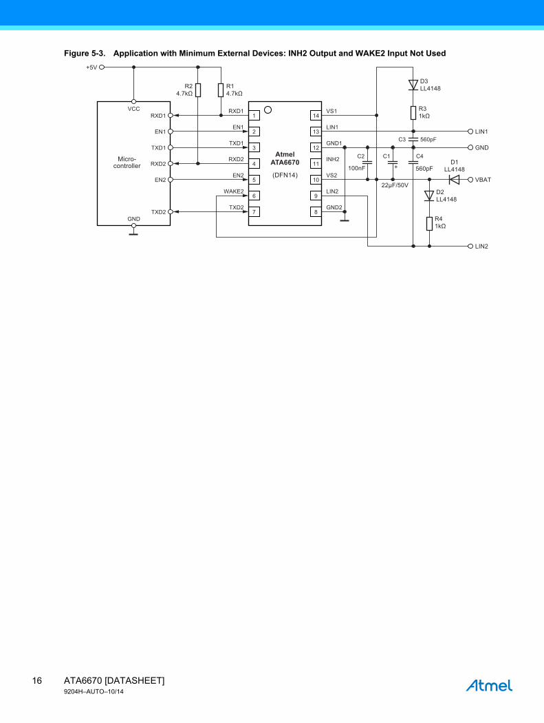
Figure 5-3. Application with Minimum External Devices: INH2 Output and WAKE2 Input Not Used
100nF 560pF
22μF/50V
1RXD1
EN1
TXD1
RXD2
EN2
WAKE2
TXD2
RXD1
EN1
+5V
TXD1
RXD2
EN2
VCC
GNDTXD2
VS1
C2 C1 C4
C3 560pF
LIN1
GND1
INH2
VS2
LIN1
GND
VBAT
LIN2
LIN2
GND2
2
3
4
5
6
7
14
13
12
11
10
9
8
R14.7kΩ
R24.7kΩ
+
R31kΩ
D3LL4148
R41kΩ
D2LL4148
AtmelATA6670
(DFN14)
Micro-controller D1
LL4148
ATA6670 [DATASHEET]9204H–AUTO–10/14
16

7. Package Information
6. Ordering Information
Extended Type Number Package Remarks
ATA6670-FFQW-1 DFN14 LIN Transceiver, Pb-free, 6k, taped and reeled.
Package Drawing Contact:[email protected]
GPC DRAWING NO. REV. TITLE
6.543-5166.03-4 1
10/11/13
Package: VDFN_4.5x3_14LExposed pad 3.9x1.6
COMMON DIMENSIONS(Unit of Measure = mm)
MIN NOM NOTEMAXSymbol
Dimensions in mm
specificationsaccording to DINtechnical drawings
0.035 0.050.0A1
3 3.12.9E
0.3 0.350.25b0.65e
0.4 0.450.35L1.6 1.71.5E2
3.9 43.8D24.5 4.64.4D
0.21 0.260.16A3
0.85 0.90.8A
D
1
Partially Plated Surface
14
PIN 1 ID E
b
L
Z 10:1
A
A3
A1
Top View
Side View
Bottom View
e
D2
1 7
14 8
E2Z
Two Step Singulation process
17ATA6670 [DATASHEET]9204H–AUTO–10/14

8. Revision History
Please note that the following page numbers referred to in this section refer to the specific revision mentioned, not to this document.
Revision No. History
9204H-AUTO-10/14• Section 6 “Ordering Information” on page 17 updated
• Section 7 “Package Information” on page 17 updated
9204G-AUTO-06/14 • Put datasheet in the latest template
9204F-AUTO-06/12 • Section 5 “Electrical Characteristics” numbers 3.2 and 4.2 on page 11 changed
9204E-AUTO-11/11 • Set datasheet from Preliminary to Standard
9204D-AUTO-10/11 • Section 6 “Electrical Characteristics” number 9.2 on page 14 added
9204C-AUTO-09/11 • Section 7 “Ordering Information” on page 18 changed
9204B-AUTO-03/11• Figure 1-1 “Block Diagram” on page 2 changed
• Section 3.15 “Fail-safe Features” on page 10 changed
ATA6670 [DATASHEET]9204H–AUTO–10/14
18

XX X XX XAtmel Corporation 1600 Technology Drive, San Jose, CA 95110 USA T: (+1)(408) 441.0311 F: (+1)(408) 436.4200 | www.atmel.com
© 2014 Atmel Corporation. / Rev.: 9204H–AUTO–10/14
Atmel®, Atmel logo and combinations thereof, Enabling Unlimited Possibilities®, and others are registered trademarks or trademarks of Atmel Corporation in U.S. and other countries. Other terms and product names may be trademarks of others.
DISCLAIMER: The information in this document is provided in connection with Atmel products. No license, express or implied, by estoppel or otherwise, to any intellectual property rightis granted by this document or in connection with the sale of Atmel products. EXCEPT AS SET FORTH IN THE ATMEL TERMS AND CONDITIONS OF SALES LOCATED ON THEATMEL WEBSITE, ATMEL ASSUMES NO LIABILITY WHATSOEVER AND DISCLAIMS ANY EXPRESS, IMPLIED OR STATUTORY WARRANTY RELATING TO ITS PRODUCTSINCLUDING, BUT NOT LIMITED TO, THE IMPLIED WARRANTY OF MERCHANTABILITY, FITNESS FOR A PARTICULAR PURPOSE, OR NON-INFRINGEMENT. IN NO EVENTSHALL ATMEL BE LIABLE FOR ANY DIRECT, INDIRECT, CONSEQUENTIAL, PUNITIVE, SPECIAL OR INCIDENTAL DAMAGES (INCLUDING, WITHOUT LIMITATION, DAMAGESFOR LOSS AND PROFITS, BUSINESS INTERRUPTION, OR LOSS OF INFORMATION) ARISING OUT OF THE USE OR INABILITY TO USE THIS DOCUMENT, EVEN IF ATMEL HASBEEN ADVISED OF THE POSSIBILITY OF SUCH DAMAGES. Atmel makes no representations or warranties with respect to the accuracy or completeness of the contents of thisdocument and reserves the right to make changes to specifications and products descriptions at any time without notice. Atmel does not make any commitment to update the informationcontained herein. Unless specifically provided otherwise, Atmel products are not suitable for, and shall not be used in, automotive applications. Atmel products are not intended,authorized, or warranted for use as components in applications intended to support or sustain life.
SAFETY-CRITICAL, MILITARY, AND AUTOMOTIVE APPLICATIONS DISCLAIMER: Atmel products are not designed for and will not be used in connection with any applications wherethe failure of such products would reasonably be expected to result in significant personal injury or death (“Safety-Critical Applications”) without an Atmel officer's specific writtenconsent. Safety-Critical Applications include, without limitation, life support devices and systems, equipment or systems for the operation of nuclear facilities and weapons systems.Atmel products are not designed nor intended for use in military or aerospace applications or environments unless specifically designated by Atmel as military-grade. Atmel products arenot designed nor intended for use in automotive applications unless specifically designated by Atmel as automotive-grade.