atlas-soc 1 april 21, 2016 · frame buffer edition. atlas-soc user manual 14 april 21, 2016 ......
TRANSCRIPT
Atlas-SoC User Manual
1 www.terasic.com April 21, 2016
Atlas-SoC User Manual
1 www.terasic.com April 21, 2016
CONTENTS
Chapter 1 Atlas-SoC Software Development Kit .......................................... 3
1.1 Package Contents ........................................................................................................................ 3
1.2 Atlas-SoC System CD ................................................................................................................... 4
1.3 Getting Help ................................................................................................................................ 4
Chapter 2 Introduction of the Atlas-SoC Board ............................................ 6
2.1 Layout and Components ............................................................................................................. 6
2.2 Block Diagram of the Atlas-SoC Board ........................................................................................ 8
Chapter 3 Using the Atlas-SoC Board ....................................................... 12
3.1 Settings of FPGA Configuration Mode ...................................................................................... 12
3.2 Board Status Elements .............................................................................................................. 14
3.3 Board Reset Elements ............................................................................................................... 15
3.4 Clock Circuitry ........................................................................................................................... 16
3.5 Peripherals Connected to the FPGA .......................................................................................... 18
3.6.1 User Push-buttons, Switches and LEDs .............................................................................. 18
3.6.2 2x20 GPIO Expansion Headers ........................................................................................... 21
3.6.3 Arduino Uno R3 Expansion Header .................................................................................... 24
3.6.4 A/D Converter and Analog Input ........................................................................................ 26
3.6 Peripherals Connected to Hard Processor System (HPS) ........................................................... 28
3.7.1 User Push-buttons and LEDs .............................................................................................. 28
3.7.2 Gigabit Ethernet ................................................................................................................. 29
3.7.3 UART .................................................................................................................................. 30
3.7.4 DDR3 Memory ................................................................................................................... 31
3.7.5 Micro SD Card Socket ......................................................................................................... 33
3.7.6 USB 2.0 OTG PHY ............................................................................................................... 34

Atlas-SoC User Manual
2 www.terasic.com April 21, 2016
3.7.7 G-sensor ............................................................................................................................ 35
3.7.8 LTC Connector .................................................................................................................... 36
Chapter 4 Appendix B ................................................................................ 38
4.1 Revision History ........................................................................................................................ 38
4.2 Copyright Statement ................................................................................................................. 38
Atlas-SoC User Manual
3 www.terasic.com April 21, 2016
Chapter 1
Atlas-SoC Software
Development Kit
The Atlas-SoC Software Development Kit presents a robust hardware design platform built around
the Altera System-on-Chip (SoC) FPGA, which combines the latest dual-core Cortex-A9 embedded
cores with industry-leading programmable logic for ultimate design flexibility. Users can now
leverage the power of tremendous re-configurability paired with a high-performance, low-power
processor system. Altera’s SoC integrates an ARM-based hard processor system (HPS) consisting of
processor, peripherals and memory interfaces tied seamlessly with the FPGA fabric using a
high-bandwidth interconnect backbone. The Atlas-SoC development board is equipped with
high-speed DDR3 memory, analog to digital capabilities, Ethernet networking, and much more that
promise many exciting applications.
The Atlas-SoC Software Development Kit contains all the tools needed to use the board in
conjunction with a computer that runs the Microsoft Windows XP or later.
1.1 PPaacckkaaggee CCoonntteennttss
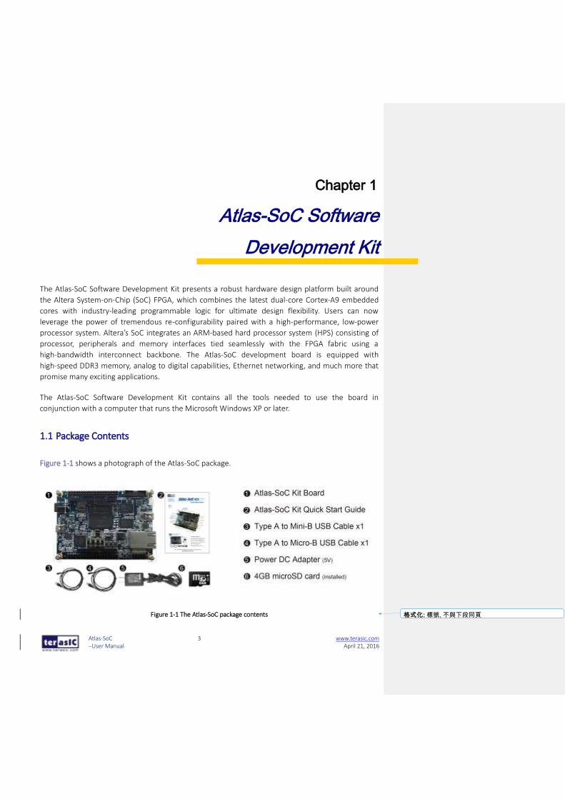
Figure 1-1 shows a photograph of the Atlas-SoC package.
Figure 1-1 The Atlas-SoC package contents 格式化: 標號, 不與下段同頁

Atlas-SoC User Manual
4 www.terasic.com April 21, 2016
The Atlas-SoC package includes:
The Atlas-SoC development board
Atlas-SoC Quick Start Guide
USB cable (Type A to Mini-B) for FPGA programming and control
USB cable (Type A to Mini-B) for UART control
5V/2A DC power adapter
4GB microSD Card (Installed)
1.2 AAttllaass--SSooCC SSyysstteemm CCDD
The Atlas-SoC System CD contains all the documents and supporting materials associated with
Atlas-SoC, including the user manual, system builder, reference designs, and device datasheets.
Users can download this system CD from the link: http://soc.terasic.com.
1.3 GGeettttiinngg HHeellpp
Here are the addresses where you can get help if you encounter any problems:
Community Support
http://www.rocketboards.org/atlas-soc
Terasic Technologies
9F., No.176, Sec.2, Gongdao 5th Rd, East Dist, Hsinchu City, 30070. Taiwan
Email: [email protected]
格式化: 標號

Atlas-SoC User Manual
5 www.terasic.com April 21, 2016
Tel.: +886-3-575-0880
Website: Atlas-SoC.terasic.com

Atlas-SoC User Manual
6 www.terasic.com April 21, 2016
Chapter 2
Introduction of the
Atlas-SoC Board
This chapter provides an introduction to the features and design characteristics of the board.
2.1 LLaayyoouutt aanndd CCoommppoonneennttss
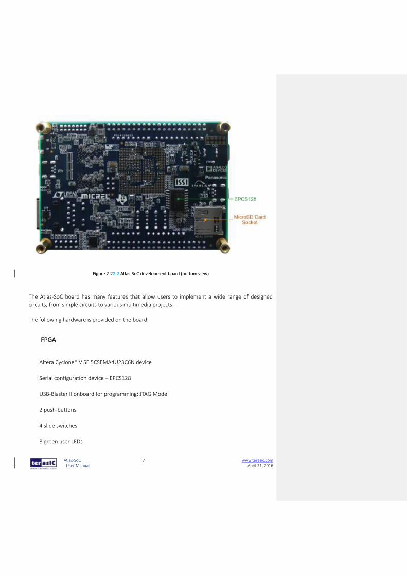
Figure 2-1 and Figure 2-2 shows a photograph of the board. It depicts the layout of the board and
indicates the location of the connectors and key components.
Figure 2-12-1 Atlas-SoC development board (top view)
Atlas-SoC User Manual
7 www.terasic.com April 21, 2016
Figure 2-22-2 Atlas-SoC development board (bottom view)
The Atlas-SoC board has many features that allow users to implement a wide range of designed
circuits, from simple circuits to various multimedia projects.
The following hardware is provided on the board:
FPGA
Altera Cyclone® V SE 5CSEMA4U23C6N device
Serial configuration device – EPCS128
USB-Blaster II onboard for programming; JTAG Mode
2 push-buttons
4 slide switches
8 green user LEDs

Atlas-SoC User Manual
8 www.terasic.com April 21, 2016
Three 50MHz clock sources from the clock generator
Two 40-pin expansion header
One Arduino expansion header (Uno R3 compatibility), can connect with Arduino shields.
One 10-pin Analog input expansion header. (shared with Arduino Analog input)
A/D converter, 4-wire SPI interface with FPGA
HPS (Hard Processor System)
925MHz Dual-core ARM Cortex-A9 processor
1GB DDR3 SDRAM (32-bit data bus)
1 Gigabit Ethernet PHY with RJ45 connector
port USB OTG, USB Micro-AB connector
Micro SD card socket
Accelerometer (I2C interface + interrupt)
UART to USB, USB Mini-B connector
Warm reset button and cold reset button
One user button and one user LED
LTC 2x7 expansion header
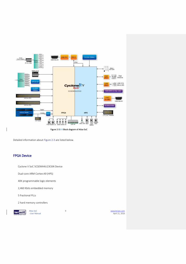
2.2 BBlloocckk DDiiaaggrraamm ooff tthhee AAttllaass--SSooCC BBooaarrdd
Figure 2-3 is the block diagram of the board. All the connections are established through the
Cyclone V SoC FPGA device to provide maximum flexibility for users. Users can configure the FPGA
to implement any system design.
Atlas-SoC User Manual
9 www.terasic.com April 21, 2016
Figure 2-32-3 Block diagram of Atlas-SoC
Detailed information about Figure 2-3 are listed below.
FFPPGGAA DDeevviiccee
Cyclone V SoC 5CSEMA4U23C6N Device
Dual-core ARM Cortex-A9 (HPS)
40K programmable logic elements
2,460 Kbits embedded memory
5 fractional PLLs
2 hard memory controllers

Atlas-SoC User Manual
10 www.terasic.com April 21, 2016
CCoonnffiigguurraattiioonn aanndd DDeebbuugg
Serial configuration device – EPCS128 on FPGA
Onboard USB-Blaster II (Mini-B USB connector)
MMeemmoorryy DDeevviiccee
1GB (2x256Mx16) DDR3 SDRAM on HPS
Micro SD card socket on HPS
CCoommmmuunniiccaattiioonn
One USB 2.0 OTG (ULPI interface with USB Micro-AB connector)
UART to USB (USB Mini-B connector)
10/100/1000 Ethernet
CCoonnnneeccttoorrss
Two 40-pin expansion headers
Arduino expansion header
One 10-pin ADC input header
One LTC connector (one Serial Peripheral Interface (SPI) Master ,one I2C and one GPIO
interface )
AADDCC
12-Bit Resolution, 500Ksps Sampling Rate. SPI Interface.
8-Channel Analog Input. Input Range : 0V ~ 4.096V.

Atlas-SoC User Manual
11 www.terasic.com April 21, 2016
SSwwiittcchheess,, BBuuttttoonnss,, aanndd IInnddiiccaattoorrss
3 user Keys (FPGA x2, HPS x1)
4 user switches (FPGA x4)
9 user LEDs (FPGA x8, HPS x 1)
2 HPS reset buttons (HPS_RESET_n and HPS_WARM_RST_n)
SSeennssoorrss
G-Sensor on HPS
PPoowweerr
5V DC input

Atlas-SoC User Manual
12 www.terasic.com April 21, 2016
Chapter 3
Using the Atlas-SoC
Board
This chapter provides an instruction to use the board and describes the peripherals.
3.1 SSeettttiinnggss ooff FFPPGGAA CCoonnffiigguurraattiioonn MMooddee
When the Atlas-SoC board is powered on, the FPGA can is configured from the SD Card (default),
but it can also be configured by the EPCS flash device as well. The MSEL[4:0] pins are used to select
the configuration scheme. It is implemented as a 6-pin DIP switch SW10 on the Atlas-SoC board, as
shown in Figure 3-1.
Figure 3-13-1 DIP switch (SW10) setting of FPP x32 mode
Atlas-SoC User Manual
13 www.terasic.com April 21, 2016
Table 3-1 shows the relation between MSEL[4:0] and DIP switch (SW10).
Table 3-1 FPGA Configuration Mode Switch (SW10)
Board Reference Signal Name Description Default
SW10.1 MSEL0
Use these pins to set the FPGA
Configuration scheme
ON (“0”)
SW10.2 MSEL1 OFF (“1”)
SW10.3 MSEL2 ON (“0”)
SW10.4 MSEL3 OFF (“1”)
SW10.5 MSEL4 ON (“0”)
SW10.6 N/A N/A N/A
Table 3-2 shows MSEL[4:0] setting for FPGA configure, and default setting is FPPx32 mode on
Atlas-SoC.
When the board is powered on and MSEL[4:0] set to “10010”, the FPGA is configured from EPCS,
which is pre-programmed with the default code. If developers wish to configure FPGA from an
application software running on Linux, the MSEL[4:0] needs to be set to “01010” before the
programming process begins. If developers using the "Linux Console with frame buffer" or "Linux
LXDE Desktop" SD Card image, the MSEL[4:0] needs to be set to “00000” before the board is
powered on.
Table 3-2 MSEL Pin Settings for FPGA Configure of Atlas-SoC
Configuration SW10.1
MSEL0
SW10.2
MSEL1
SW10.3
MSEL2
SW10.4
MSEL3
SW10.5
MSEL4
SW10.6
Description
AS ON OFF ON ON OFF N/A FPGA configured from EPCS
FPPx32 (Default) ON OFF ON OFF ON N/A FPGA configured from HPS
software: Linux (default)
FPPx16 ON ON ON ON ON N/A
FPGA configured from HPS
software: U-Boot, with image
stored on the SD card, like LXDE
Desktop or console Linux with
frame buffer edition.
Atlas-SoC User Manual
14 www.terasic.com April 21, 2016
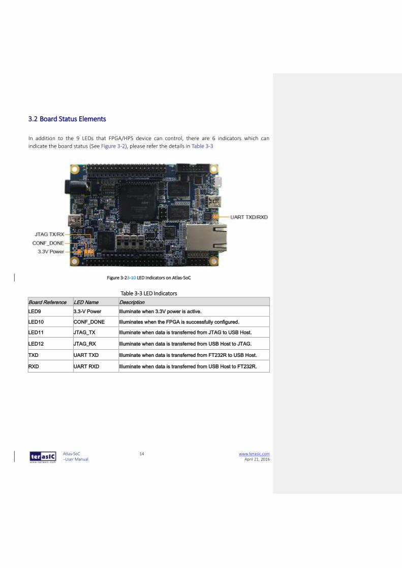
3.2 BBooaarrdd SSttaattuuss EElleemmeennttss
In addition to the 9 LEDs that FPGA/HPS device can control, there are 6 indicators which can
indicate the board status (See Figure 3-2), please refer the details in Table 3-3
Figure 3-23-10 LED Indicators on Atlas-SoC
Table 3-3 LED Indicators
Board Reference LED Name Description
LED9 3.3-V Power Illuminate when 3.3V power is active.
LED10 CONF_DONE Illuminates when the FPGA is successfully configured.
LED11 JTAG_TX Illuminate when data is transferred from JTAG to USB Host.
LED12 JTAG_RX Illuminate when data is transferred from USB Host to JTAG.
TXD UART TXD Illuminate when data is transferred from FT232R to USB Host.
RXD UART RXD Illuminate when data is transferred from USB Host to FT232R.
Atlas-SoC User Manual
15 www.terasic.com April 21, 2016
3.3 BBooaarrdd RReesseett EElleemmeennttss
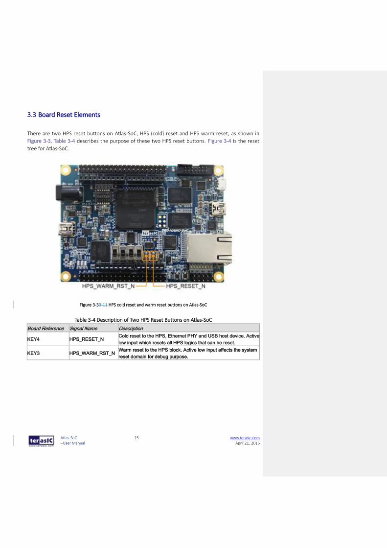
There are two HPS reset buttons on Atlas-SoC, HPS (cold) reset and HPS warm reset, as shown in
Figure 3-3. Table 3-4 describes the purpose of these two HPS reset buttons. Figure 3-4 is the reset
tree for Atlas-SoC.
Figure 3-33-11 HPS cold reset and warm reset buttons on Atlas-SoC
Table 3-4 Description of Two HPS Reset Buttons on Atlas-SoC
Board Reference Signal Name Description
KEY4 HPS_RESET_N Cold reset to the HPS, Ethernet PHY and USB host device. Active
low input which resets all HPS logics that can be reset.
KEY3 HPS_WARM_RST_N Warm reset to the HPS block. Active low input affects the system
reset domain for debug purpose.

Atlas-SoC User Manual
16 www.terasic.com April 21, 2016
Figure 3-43-12 HPS reset tree on Atlas-SoC board
3.4 CClloocckk CCiirrccuuiittrryy
Figure 3-5 shows the default frequency of all external clocks to the Cyclone V SoC FPGA. A clock
generator is used to distribute clock signals with low jitter. The two 50MHz clock signals connected
to the FPGA are used as clock sources for user logic. Three 25MHz clock signal are connected to two
HPS clock inputs, and the other one is connected to the clock input of Gigabit Ethernet Transceiver.
One 24MHz clock signal is connected to the USB controller for USB Blaster II circuit and FPGA. One
24MHz clock signals are connected to the clock inputs of USB OTG PHY. The associated pin
assignment for clock inputs to FPGA I/O pins is listed in Table 3-5.

Atlas-SoC User Manual
17 www.terasic.com April 21, 2016
Figure 3-53-13 Block diagram of the clock distribution on Atlas-SoC
Table 3-5 Pin Assignment of Clock Inputs
Signal Name FPGA Pin No. Description I/O Standard
FPGA_CLK1_50 PIN_V11 50 MHz clock input 3.3V
FPGA_CLK2_50 PIN_Y13 50 MHz clock input 3.3V
FPGA_CLK3_50 PIN_E11 50 MHz clock input (share with FPGA_CLK1_50) 3.3V
HPS_CLK1_25 PIN_E20 25 MHz clock input 3.3V
HPS_CLK2_25 PIN_D20 25 MHz clock input 3.3V
Atlas-SoC User Manual
18 www.terasic.com April 21, 2016
3.5 PPeerriipphheerraallss CCoonnnneecctteedd ttoo tthhee FFPPGGAA
This section describes the interfaces connected to the FPGA. Users can control or monitor different
interfaces with user logic from the FPGA.
3.6.1 User Push-buttons, Switches and LEDs
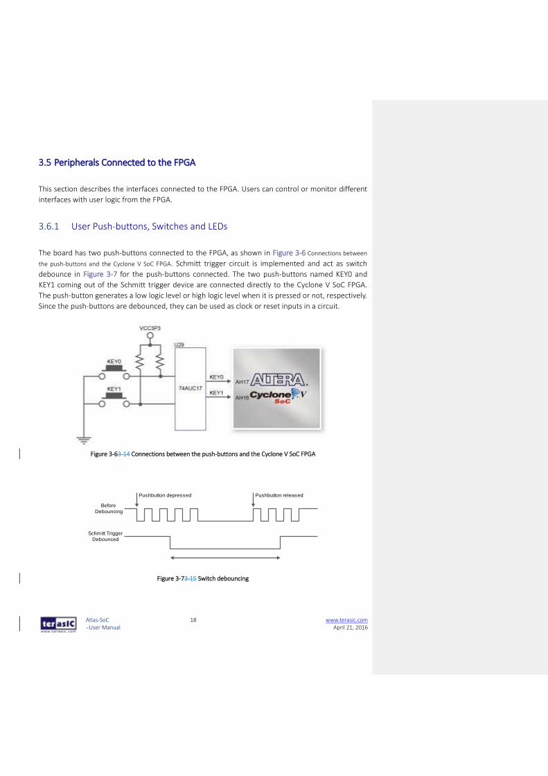
The board has two push-buttons connected to the FPGA, as shown in Figure 3-6 Connections between
the push-buttons and the Cyclone V SoC FPGA. Schmitt trigger circuit is implemented and act as switch
debounce in Figure 3-7 for the push-buttons connected. The two push-buttons named KEY0 and
KEY1 coming out of the Schmitt trigger device are connected directly to the Cyclone V SoC FPGA.
The push-button generates a low logic level or high logic level when it is pressed or not, respectively.
Since the push-buttons are debounced, they can be used as clock or reset inputs in a circuit.
Figure 3-63-14 Connections between the push-buttons and the Cyclone V SoC FPGA
Pushbutton releasedPushbutton depressed
Before
Debouncing
Schmitt Trigger
Debounced
Figure 3-73-15 Switch debouncing

Atlas-SoC User Manual
19 www.terasic.com April 21, 2016
There are four slide switches connected to the FPGA, as shown in Figure 3-8. These switches are not
debounced and to be used as level-sensitive data inputs to a circuit. Each switch is connected
directly and individually to the FPGA. When the switch is set to the DOWN position (towards the
edge of the board), it generates a low logic level to the FPGA. When the switch is set to the UP
position, a high logic level is generated to the FPGA.
Figure 3-83-16 Connections between the slide switches and the Cyclone V SoC FPGA
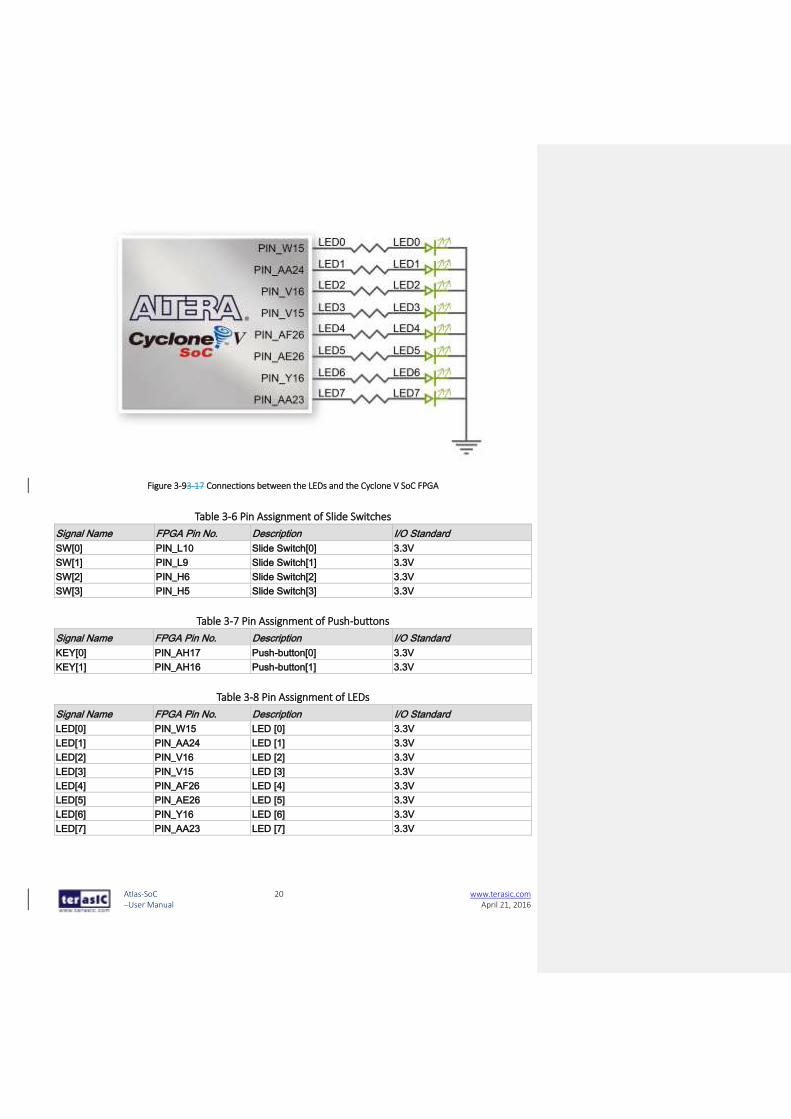
There are also eight user-controllable LEDs connected to the FPGA. Each LED is driven directly and
individually by the Cyclone V SoC FPGA; driving its associated pin to a high logic level or low level to
turn the LED on or off, respectively. Figure 3-9 shows the connections between LEDs and Cyclone V
SoC FPGA. Table 3-6, Table 3-7 and Table 3-8 list the pin assignment of user push-buttons, switches,
and LEDs.
Atlas-SoC User Manual
20 www.terasic.com April 21, 2016
Figure 3-93-17 Connections between the LEDs and the Cyclone V SoC FPGA
Table 3-6 Pin Assignment of Slide Switches
Signal Name FPGA Pin No. Description I/O Standard
SW[0] PIN_L10 Slide Switch[0] 3.3V
SW[1] PIN_L9 Slide Switch[1] 3.3V
SW[2] PIN_H6 Slide Switch[2] 3.3V
SW[3] PIN_H5 Slide Switch[3] 3.3V
Table 3-7 Pin Assignment of Push-buttons
Signal Name FPGA Pin No. Description I/O Standard
KEY[0] PIN_AH17 Push-button[0] 3.3V
KEY[1] PIN_AH16 Push-button[1] 3.3V
Table 3-8 Pin Assignment of LEDs
Signal Name FPGA Pin No. Description I/O Standard
LED[0] PIN_W15 LED [0] 3.3V
LED[1] PIN_AA24 LED [1] 3.3V
LED[2] PIN_V16 LED [2] 3.3V
LED[3] PIN_V15 LED [3] 3.3V
LED[4] PIN_AF26 LED [4] 3.3V
LED[5] PIN_AE26 LED [5] 3.3V
LED[6] PIN_Y16 LED [6] 3.3V
LED[7] PIN_AA23 LED [7] 3.3V
Atlas-SoC User Manual
21 www.terasic.com April 21, 2016
3.6.2 2x20 GPIO Expansion Headers
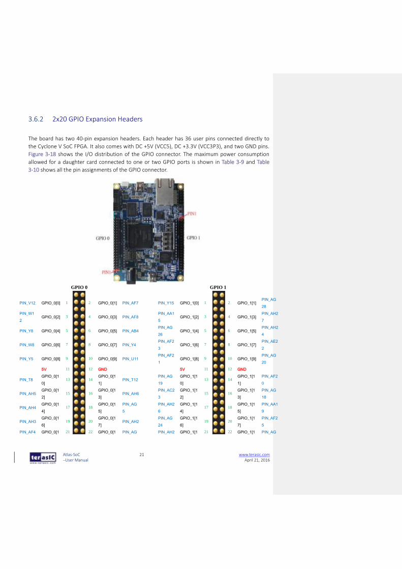
The board has two 40-pin expansion headers. Each header has 36 user pins connected directly to
the Cyclone V SoC FPGA. It also comes with DC +5V (VCC5), DC +3.3V (VCC3P3), and two GND pins.
Figure 3-18 shows the I/O distribution of the GPIO connector. The maximum power consumption
allowed for a daughter card connected to one or two GPIO ports is shown in Table 3-9 and Table
3-10 shows all the pin assignments of the GPIO connector.
GPIO 0
(JP1)
GPIO 1
(JP7)
PIN_V12 GPIO_0[0] 1 2 GPIO_0[1] PIN_AF7 PIN_Y15 GPIO_1[0] 1 2 GPIO_1[1] PIN_AG
28
PIN_W1
2 GPIO_0[2] 3 4 GPIO_0[3] PIN_AF8
PIN_AA1
5 GPIO_1[2] 3 4 GPIO_1[3]
PIN_AH2
7
PIN_Y8 GPIO_0[4] 5 6 GPIO_0[5] PIN_AB4 PIN_AG
26 GPIO_1[4] 5 6 GPIO_1[5]
PIN_AH2
4
PIN_W8 GPIO_0[6] 7 8 GPIO_0[7] PIN_Y4 PIN_AF2
3 GPIO_1[6] 7 8 GPIO_1[7]
PIN_AE2
2
PIN_Y5 GPIO_0[8] 9 10 GPIO_0[9] PIN_U11 PIN_AF2
1 GPIO_1[8] 9 10 GPIO_1[9]
PIN_AG
20
5V 11 12 GND 5V 11 12 GND
PIN_T8 GPIO_0[1
0] 13 14
GPIO_0[1
1] PIN_T12
PIN_AG
19
GPIO_1[1
0] 13 14
GPIO_1[1
1]
PIN_AF2
0
PIN_AH5 GPIO_0[1
2] 15 16
GPIO_0[1
3] PIN_AH6
PIN_AC2
3
GPIO_1[1
2] 15 16
GPIO_1[1
3]
PIN_AG
18
PIN_AH4 GPIO_0[1
4] 17 18
GPIO_0[1
5]
PIN_AG
5
PIN_AH2
6
GPIO_1[1
4] 17 18
GPIO_1[1
5]
PIN_AA1
9
PIN_AH3 GPIO_0[1
6] 19 20
GPIO_0[1
7] PIN_AH2
PIN_AG
24
GPIO_1[1
6] 19 20
GPIO_1[1
7]
PIN_AF2
5
PIN_AF4 GPIO_0[1 21 22 GPIO_0[1 PIN_AG PIN_AH2 GPIO_1[1 21 22 GPIO_1[1 PIN_AG
Atlas-SoC User Manual
22 www.terasic.com April 21, 2016
Table 3-9 Voltage and Max. Current Limit of Expansion Header(s)
Supplied Voltage Max. Current Limit
5V 1A (depend on the power adapter specification.)
3.3V 1.5A
Table 3-10 Pin Assignment of Expansion Headers
Signal Name FPGA Pin No. Description I/O Standard
GPIO_0[0] PIN_V12 GPIO Connection 0[0] 3.3V
GPIO_0[1] PIN_AF7 GPIO Connection 0[1] 3.3V
GPIO_0[2] PIN_W12 GPIO Connection 0[2] 3.3V
GPIO_0[3] PIN_AF8 GPIO Connection 0[3] 3.3V
GPIO_0[4] PIN_Y8 GPIO Connection 0[4] 3.3V
GPIO_0[5] PIN_AB4 GPIO Connection 0[5] 3.3V
GPIO_0[6] PIN_W8 GPIO Connection 0[6] 3.3V
GPIO_0[7] PIN_Y4 GPIO Connection 0[7] 3.3V
GPIO_0[8] PIN_Y5 GPIO Connection 0[8] 3.3V
GPIO_0[9] PIN_U11 GPIO Connection 0[9] 3.3V
GPIO_0[10] PIN_T8 GPIO Connection 0[10] 3.3V
GPIO_0[11] PIN_T12 GPIO Connection 0[11] 3.3V
GPIO_0[12] PIN_AH5 GPIO Connection 0[12] 3.3V
GPIO_0[13] PIN_AH6 GPIO Connection 0[13] 3.3V
GPIO_0[14] PIN_AH4 GPIO Connection 0[14] 3.3V
8] 9] 6 3 8] 9] 23
PIN_AF5 GPIO_0[2
0] 23 24
GPIO_0[2
1] PIN_AE4
PIN_AE1
9
GPIO_1[2
0] 23 24
GPIO_1[2
1]
PIN_AF1
8
PIN_T13 GPIO_0[2
2] 25 26
GPIO_0[2
3] PIN_T11
PIN_AD1
9
GPIO_1[2
2] 25 26
GPIO_1[2
3]
PIN_AE2
0
PIN_AE7 GPIO_0[2
4] 27 28
GPIO_0[2
5] PIN_AF6
PIN_AE2
4
GPIO_1[2
4] 27 28
GPIO_1[2
5]
PIN_AD2
0
3.3V 29 30 GND 3.3V 29 30 GND
PIN_AF9 GPIO_0[2
6] 31 32
GPIO_0[2
7] PIN_AE8
PIN_AF2
2
GPIO_1[2
6] 31 32
GPIO_1[2
7]
PIN_AH2
2
PIN_AD1
0
GPIO_0[2
8] 33 34
GPIO_0[2
9] PIN_AE9
PIN_AH1
9
GPIO_1[2
8] 33 34
GPIO_1[2
9]
PIN_AH2
1
PIN_AD1
1
GPIO_0[3
0] 35 36
GPIO_0[3
1]
PIN_AF1
0
PIN_AG
21
GPIO_1[3
0] 35 36
GPIO_1[3
1]
PIN_AH1
8
PIN_AD1
2
GPIO_0[3
2] 37 38
GPIO_0[3
3]
PIN_AE1
1
PIN_AD2
3
GPIO_1[3
2] 37 38
GPIO_1[3
3]
PIN_AE2
3
PIN_AF1
1
GPIO_0[3
4] 39 40
GPIO_0[3
5]
PIN_AE1
2
PIN_AA1
8
GPIO_1[3
4] 39 40
GPIO_1[3
5]
PIN_AC2
2
Figure 3-10 GPIO Pin Arrangement

Atlas-SoC User Manual
23 www.terasic.com April 21, 2016
GPIO_0[15] PIN_AG5 GPIO Connection 0[15] 3.3V
GPIO_0[16] PIN_AH3 GPIO Connection 0[16] 3.3V
GPIO_0[17] PIN_AH2 GPIO Connection 0[17] 3.3V
GPIO_0[18] PIN_AF4 GPIO Connection 0[18] 3.3V
GPIO_0[19] PIN_AG6 GPIO Connection 0[19] 3.3V
GPIO_0[20] PIN_AF5 GPIO Connection 0[20] 3.3V
GPIO_0[21] PIN_AE4 GPIO Connection 0[21] 3.3V
GPIO_0[22] PIN_T13 GPIO Connection 0[22] 3.3V
GPIO_0[23] PIN_T11 GPIO Connection 0[23] 3.3V
GPIO_0[24] PIN_AE7 GPIO Connection 0[24] 3.3V
GPIO_0[25] PIN_AF6 GPIO Connection 0[25] 3.3V
GPIO_0[26] PIN_AF9 GPIO Connection 0[26] 3.3V
GPIO_0[27] PIN_AE8 GPIO Connection 0[27] 3.3V
GPIO_0[28] PIN_AD10 GPIO Connection 0[28] 3.3V
GPIO_0[29] PIN_AE9 GPIO Connection 0[29] 3.3V
GPIO_0[30] PIN_AD11 GPIO Connection 0[30] 3.3V
GPIO_0[31] PIN_AF10 GPIO Connection 0[31] 3.3V
GPIO_0[32] PIN_AD12 GPIO Connection 0[32] 3.3V
GPIO_0[33] PIN_AE11 GPIO Connection 0[33] 3.3V
GPIO_0[34] PIN_AF11 GPIO Connection 0[34] 3.3V
GPIO_0[35] PIN_AE12 GPIO Connection 0[35] 3.3V
GPIO_1[0] PIN_Y15 GPIO Connection 1[0] 3.3V
GPIO_1[1] PIN_AG28 GPIO Connection 1[1] 3.3V
GPIO_1[2] PIN_AA15 GPIO Connection 1[2] 3.3V
GPIO_1[3] PIN_AH27 GPIO Connection 1[3] 3.3V
GPIO_1[4] PIN_AG26 GPIO Connection 1[4] 3.3V
GPIO_1[5] PIN_AH24 GPIO Connection 1[5] 3.3V
GPIO_1[6] PIN_AF23 GPIO Connection 1[6] 3.3V
GPIO_1[7] PIN_AE22 GPIO Connection 1[7] 3.3V
GPIO_1[8] PIN_AF21 GPIO Connection 1[8] 3.3V
GPIO_1[9] PIN_AG20 GPIO Connection 1[9] 3.3V
GPIO_1[10] PIN_AG19 GPIO Connection 1[10] 3.3V
GPIO_1[11] PIN_AF20 GPIO Connection 1[11] 3.3V
GPIO_1[12] PIN_AC23 GPIO Connection 1[12] 3.3V
GPIO_1[13] PIN_AG18 GPIO Connection 1[13] 3.3V
GPIO_1[14] PIN_AH26 GPIO Connection 1[14] 3.3V
GPIO_1[15] PIN_AA19 GPIO Connection 1[15] 3.3V
GPIO_1[16] PIN_AG24 GPIO Connection 1[16] 3.3V
GPIO_1[17] PIN_AF25 GPIO Connection 1[17] 3.3V
GPIO_1[18] PIN_AH23 GPIO Connection 1[18] 3.3V
GPIO_1[19] PIN_AG23 GPIO Connection 1[19] 3.3V
GPIO_1[20] PIN_AE19 GPIO Connection 1[20] 3.3V
GPIO_1[21] PIN_AF18 GPIO Connection 1[21] 3.3V
GPIO_1[22] PIN_AD19 GPIO Connection 1[22] 3.3V
GPIO_1[23] PIN_AE20 GPIO Connection 1[23] 3.3V

Atlas-SoC User Manual
24 www.terasic.com April 21, 2016
GPIO_1[24] PIN_AE24 GPIO Connection 1[24] 3.3V
GPIO_1[25] PIN_AD20 GPIO Connection 1[25] 3.3V
GPIO_1[26] PIN_AF22 GPIO Connection 1[26] 3.3V
GPIO_1[27] PIN_AH22 GPIO Connection 1[27] 3.3V
GPIO_1[28] PIN_AH19 GPIO Connection 1[28] 3.3V
GPIO_1[29] PIN_AH21 GPIO Connection 1[29] 3.3V
GPIO_1[30] PIN_AG21 GPIO Connection 1[30] 3.3V
GPIO_1[31] PIN_AH18 GPIO Connection 1[31] 3.3V
GPIO_1[32] PIN_AD23 GPIO Connection 1[32] 3.3V
GPIO_1[33] PIN_AE23 GPIO Connection 1[33] 3.3V
GPIO_1[34] PIN_AA18 GPIO Connection 1[34] 3.3V
GPIO_1[35] PIN_AC22 GPIO Connection 1[35] 3.3V
3.6.3 Arduino Uno R3 Expansion Header
The board provides Arduino Uno revision 3 compatibility expansion header which comes with four
independent headers. The expansion header has 17 user pins (16pins GPIO and 1pin Reset)
connected directly to the Cyclone V SoC FPGA. 6-pins Analog input connects to ADC, and also
provides DC +9V (VCC9), DC +5V (VCC5), DC +3.3V (VCC3P3 and IOREF), and three GND pins.
Please refer to Figure 3-11 for detailed pin-out information. The blue font represents the Arduino
Uno R3 board pin-out definition.

Atlas-SoC User Manual
25 www.terasic.com April 21, 2016
Figure 3-113-18 lists the all the pin-out signal name of the Arduino Uno connector. The blue font represents
the Arduino pin-out definition.
The 16 GPIO pins are provided to the Arduino Header for digital I/O. Table 3-11 lists the all the pin
assignments of the Arduino Uno connector (digital), signal names relative to the Cyclone V SoC
FPGA.
Table 3-11 Pin Assignments for Arduino Uno Expansion Header connector
Schematic
Signal Name FPGA Pin No. Description
Specific features
For Arduino I/O Standard
Arduino_IO0 PIN_AG13 Arduino IO0 RXD
3.3-V
Arduino_IO1 PIN_AF13 Arduino IO1 TXD
3.3-V
Arduino_IO2 PIN_AG10 Arduino IO2
3.3-V

Atlas-SoC User Manual
26 www.terasic.com April 21, 2016
Arduino_IO3 PIN_AG9 Arduino IO3
3.3-V
Arduino_IO4 PIN_U14 Arduino IO4
3.3-V
Arduino_IO5 PIN_U13 Arduino IO5
3.3-V
Arduino_IO6 PIN_AG8 Arduino IO6
3.3-V
Arduino_IO7 PIN_AH8 Arduino IO7
3.3-V
Arduino_IO8 PIN_AF17 Arduino IO8
3.3-V
Arduino_IO9 PIN_AE15 Arduino IO9
3.3-V
Arduino_IO10 PIN_AF15 Arduino IO10 SS
3.3-V
Arduino_IO11 PIN_AG16 Arduino IO11 MOSI
3.3-V
Arduino_IO12 PIN_AH11 Arduino IO12 MISO
3.3-V
Arduino_IO13 PIN_AH12 Arduino IO13 SCK
3.3-V
Arduino_IO14 PIN_AH9 Arduino IO14 SDA
3.3-V
Arduino_IO15 PIN_AG11 Arduino IO15 SCL
3.3-V
Arduino_Reset_n PIN_AH7
Reset signal, low active. 3.3-V
Besides 16 pins for digital GPIO, there are also 6 analog inputs on the Arduino Uno R3 Expansion
Header (ADC_IN0 ~ ADC_IN5). Consequently, we use ADC LTC2308 from Linear Technology on the
board for possible future analog-to-digital applications. We will introduce in the next section.
3.6.4 A/D Converter and Analog Input
The Atlas-SoC has an analog-to-digital converter (LTC2308).
The LTC2308 is a low noise, 500ksps, 8-channel, 12-bit ADC with a SPI/MICROWIRE compatible serial
interface. This ADC includes an internal reference and a fully differential sample-and-hold circuit to

Atlas-SoC User Manual
27 www.terasic.com April 21, 2016
reduce common mode noise. The internal conversion clock allows the external serial output data
clock (SCK) to operate at any frequency up to 40MHz.
It can be configured to accept eight input signals at inputs ADC_IN0 through ADC_IN7. These eight
input signals are connected to a 2x5 header, as shown in Figure 3-12.
Figure 3-123-19 Signals of the 2x5 Header
These Analog inputs are shared with the Arduino's analog input pin (ADC_IN0 ~ ADC_IN5), Figure
3-13 shows the connections between the FPGA, 2x5 header, Arduino Analog input, and the A/D
converter.
More information about the A/D converter chip can be found on manufacturer’s website
(http://www.linear.com/product/LTC2308).

Atlas-SoC User Manual
28 www.terasic.com April 21, 2016
Figure 3-133-20 Connections between the FPGA, 2x5 header, and the A/D converter
Table 3-12 Pin Assignment of ADC
Signal Name FPGA Pin No. Description I/O Standard
ADC_CONVST PIN_U9 Conversion Start 3.3V
ADC_SCK PIN_V10 Serial Data Clock 3.3V
ADC_SDI PIN_AC4 Serial Data Input (FPGA to ADC) 3.3V
ADC_SDO PIN_AD4 Serial Data Out (ADC to FPGA) 3.3V
3.6 PPeerriipphheerraallss CCoonnnneecctteedd ttoo HHaarrdd PPrroocceessssoorr SSyysstteemm ((HHPPSS))
This section introduces the interfaces connected to the HPS section of the Cyclone V SoC FPGA.
Users can access these interfaces via the HPS processor.
33..77..11 UUsseerr PPuusshh--bbuuttttoonnss aanndd LLEEDDss
Similar to the FPGA, the HPS also has its set of switches, buttons, LEDs, and other interfaces
connected exclusively. Users can control these interfaces to monitor the status of HPS.

Atlas-SoC User Manual
29 www.terasic.com April 21, 2016
Table 3-13 gives the pin assignment of all the LEDs, switches, and push-buttons.
Table 3-13 Pin Assignment of LEDs, Switches and Push-buttons
Signal Name FPGA Pin No. HPS GPIO Register/bit Function
HPS_KEY PIN_J18 GPIO54 GPIO1[25] I/O
HPS_LED PIN_A20 GPIO53 GPIO1[24] I/O
33..77..22 GGiiggaabbiitt EEtthheerrnneett
The board supports Gigabit Ethernet transfer by an external Micrel KSZ9031RN PHY chip and HPS
Ethernet MAC function. The KSZ9031RN chip with integrated 10/100/1000 Mbps Gigabit Ethernet
transceiver also supports RGMII MAC interface. Figure 3-14 shows the connections between the HPS,
Gigabit Ethernet PHY, and RJ-45 connector.
The pin assignment associated to Gigabit Ethernet interface is listed in Table 3-14. More information
about the KSZ9031RN PHY chip and its datasheet, as well as the application notes, which are
available on the manufacturer’s website
(http://www.micrel.com/index.php/products/lan-solutions/phys/article/2-ksz9031rnx.html).
Figure 3-143-21 Connections between the HPS and Gigabit Ethernet
Atlas-SoC User Manual
30 www.terasic.com April 21, 2016
Table 3-14 Pin Assignment of Gigabit Ethernet PHY
Signal Name FPGA Pin No. Description I/O Standard
HPS_ENET_TX_EN PIN_A12 GMII and MII transmit enable 3.3V
HPS_ENET_TX_DATA[0] PIN_A16 MII transmit data[0] 3.3V
HPS_ENET_TX_DATA[1] PIN_J14 MII transmit data[1] 3.3V
HPS_ENET_TX_DATA[2] PIN_A15 MII transmit data[2] 3.3V
HPS_ENET_TX_DATA[3] PIN_D17 MII transmit data[3] 3.3V
HPS_ENET_RX_DV PIN_J13 GMII and MII receive data valid 3.3V
HPS_ENET_RX_DATA[0] PIN_A14 GMII and MII receive data[0] 3.3V
HPS_ENET_RX_DATA[1] PIN_A11 GMII and MII receive data[1] 3.3V
HPS_ENET_RX_DATA[2] PIN_C15 GMII and MII receive data[2] 3.3V
HPS_ENET_RX_DATA[3] PIN_A9 GMII and MII receive data[3] 3.3V
HPS_ENET_RX_CLK PIN_J12 GMII and MII receive clock 3.3V
HPS_ENET_RESET_N PIN_B14 Hardware Reset Signal 3.3V
HPS_ENET_MDIO PIN_E16 Management Data 3.3V
HPS_ENET_MDC PIN_A13 Management Data Clock Reference 3.3V
HPS_ENET_INT_N PIN_B14 Interrupt Open Drain Output 3.3V
HPS_ENET_GTX_CLK PIN_J15 GMII Transmit Clock 3.3V
There are two LEDs, green LED (LEDG) and yellow LED (LEDY), which represent the status of
Ethernet PHY (KSZ9031RN). The LED control signals are connected to the LEDs on the RJ45
connector. The state and definition of LEDG and LEDY are listed in Table 3-15. For instance, the
connection from board to Gigabit Ethernet is established once the LEDG lights on.
Table 3-15 State and Definition of LED Mode Pins
LED (State) LED (Definition) Link /Activity
LEDG LEDY LEDG LEDY
H H OFF OFF Link off
L H ON OFF 1000 Link / No Activity
Toggle H Blinking OFF 1000 Link / Activity (RX, TX)
H L OFF ON 100 Link / No Activity
H Toggle OFF Blinking 100 Link / Activity (RX, TX)
L L ON ON 10 Link/ No Activity
Toggle Toggle Blinking Blinking 10 Link / Activity (RX, TX)
33..77..33 UUAARRTT
The board has one UART interface connected for communication with the HPS. This interface
doesn’t support HW flow control signals. The physical interface is implemented by UART-USB
onboard bridge from a FT232R chip to the host with an USB Mini-B connector. More information
about the chip is available on the manufacturer’s website
(http://www.ftdichip.com/Products/ICs/FT232R.htm ). Figure 3-15 shows the connections between

Atlas-SoC User Manual
31 www.terasic.com April 21, 2016
the HPS, FT232R chip, and the USB Mini-B connector. Table 3-16 lists the pin assignment of UART
interface connected to the HPS.
Figure 3-153-22 Connections between the HPS and FT232R Chip
Table 3-16 Pin Assignment of UART Interface
Signal Name FPGA Pin No. Description I/O Standard
HPS_UART_RX PIN_A22 HPS UART Receiver 3.3V
HPS_UART_TX PIN_B21 HPS UART Transmitter 3.3V
HPS_CONV_USB_N PIN_C6 Reserve 3.3V
33..77..44 DDDDRR33 MMeemmoorryy
The DDR3 devices connected to the HPS are the exact same model as the ones connected to the
FPGA. The capacity is 1GB and the data bandwidth is in 32-bit, comprised of two x16 devices with a
single address/command bus. The signals are connected to the dedicated Hard Memory Controller
for HPS I/O banks and the target speed is 400 MHz. Table 3-17 lists the pin assignment of DDR3 and
its description with I/O standard.
Table 3-17 Pin Assignment of DDR3 Memory
Signal Name FPGA Pin No. Description I/O Standard
HPS_DDR3_A[0] PIN_C28 HPS DDR3 Address[0] SSTL-15 Class I
HPS_DDR3_A[1] PIN_B28 HPS DDR3 Address[1] SSTL-15 Class I
HPS_DDR3_A[2] PIN_E26 HPS DDR3 Address[2] SSTL-15 Class I
HPS_DDR3_A[3] PIN_D26 HPS DDR3 Address[3] SSTL-15 Class I
HPS_DDR3_A[4] PIN_J21 HPS DDR3 Address[4] SSTL-15 Class I
HPS_DDR3_A[5] PIN_J20 HPS DDR3 Address[5] SSTL-15 Class I

Atlas-SoC User Manual
32 www.terasic.com April 21, 2016
HPS_DDR3_A[6] PIN_C26 HPS DDR3 Address[6] SSTL-15 Class I
HPS_DDR3_A[7] PIN_B26 HPS DDR3 Address[7] SSTL-15 Class I
HPS_DDR3_A[8] PIN_F26 HPS DDR3 Address[8] SSTL-15 Class I
HPS_DDR3_A[9] PIN_F25 HPS DDR3 Address[9] SSTL-15 Class I
HPS_DDR3_A[10] PIN_A24 HPS DDR3 Address[10] SSTL-15 Class I
HPS_DDR3_A[11] PIN_B24 HPS DDR3 Address[11] SSTL-15 Class I
HPS_DDR3_A[12] PIN_D24 HPS DDR3 Address[12] SSTL-15 Class I
HPS_DDR3_A[13] PIN_C24 HPS DDR3 Address[13] SSTL-15 Class I
HPS_DDR3_A[14] PIN_G23 HPS DDR3 Address[14] SSTL-15 Class I
HPS_DDR3_BA[0] PIN_A27 HPS DDR3 Bank Address[0] SSTL-15 Class I
HPS_DDR3_BA[1] PIN_H25 HPS DDR3 Bank Address[1] SSTL-15 Class I
HPS_DDR3_BA[2] PIN_G25 HPS DDR3 Bank Address[2] SSTL-15 Class I
HPS_DDR3_CAS_n PIN_A26 DDR3 Column Address Strobe SSTL-15 Class I
HPS_DDR3_CKE PIN_L28 HPS DDR3 Clock Enable SSTL-15 Class I
HPS_DDR3_CK_n PIN_N20 HPS DDR3 Clock Differential 1.5-V SSTL Class I
HPS_DDR3_CK_p PIN_N21 HPS DDR3 Clock p Differential 1.5-V SSTL Class I
HPS_DDR3_CS_n PIN_L21 HPS DDR3 Chip Select SSTL-15 Class I
HPS_DDR3_DM[0] PIN_G28 HPS DDR3 Data Mask[0] SSTL-15 Class I
HPS_DDR3_DM[1] PIN_P28 HPS DDR3 Data Mask[1] SSTL-15 Class I
HPS_DDR3_DM[2] PIN_W28 HPS DDR3 Data Mask[2] SSTL-15 Class I
HPS_DDR3_DM[3] PIN_AB28 HPS DDR3 Data Mask[3] SSTL-15 Class I
HPS_DDR3_DQ[0] PIN_J25 HPS DDR3 Data[0] SSTL-15 Class I
HPS_DDR3_DQ[1] PIN_J24 HPS DDR3 Data[1] SSTL-15 Class I
HPS_DDR3_DQ[2] PIN_E28 HPS DDR3 Data[2] SSTL-15 Class I
HPS_DDR3_DQ[3] PIN_D27 HPS DDR3 Data[3] SSTL-15 Class I
HPS_DDR3_DQ[4] PIN_J26 HPS DDR3 Data[4] SSTL-15 Class I
HPS_DDR3_DQ[5] PIN_K26 HPS DDR3 Data[5] SSTL-15 Class I
HPS_DDR3_DQ[6] PIN_G27 HPS DDR3 Data[6] SSTL-15 Class I
HPS_DDR3_DQ[7] PIN_F28 HPS DDR3 Data[7] SSTL-15 Class I
HPS_DDR3_DQ[8] PIN_K25 HPS DDR3 Data[8] SSTL-15 Class I
HPS_DDR3_DQ[9] PIN_L25 HPS DDR3 Data[9] SSTL-15 Class I
HPS_DDR3_DQ[10] PIN_J27 HPS DDR3 Data[10] SSTL-15 Class I
HPS_DDR3_DQ[11] PIN_J28 HPS DDR3 Data[11] SSTL-15 Class I
HPS_DDR3_DQ[12] PIN_M27 HPS DDR3 Data[12] SSTL-15 Class I
HPS_DDR3_DQ[13] PIN_M26 HPS DDR3 Data[13] SSTL-15 Class I
HPS_DDR3_DQ[14] PIN_M28 HPS DDR3 Data[14] SSTL-15 Class I
HPS_DDR3_DQ[15] PIN_N28 HPS DDR3 Data[15] SSTL-15 Class I
HPS_DDR3_DQ[16] PIN_N24 HPS DDR3 Data[16] SSTL-15 Class I
HPS_DDR3_DQ[17] PIN_N25 HPS DDR3 Data[17] SSTL-15 Class I
HPS_DDR3_DQ[18] PIN_T28 HPS DDR3 Data[18] SSTL-15 Class I
HPS_DDR3_DQ[19] PIN_U28 HPS DDR3 Data[19] SSTL-15 Class I
HPS_DDR3_DQ[20] PIN_N26 HPS DDR3 Data[20] SSTL-15 Class I
HPS_DDR3_DQ[21] PIN_N27 HPS DDR3 Data[21] SSTL-15 Class I
HPS_DDR3_DQ[22] PIN_R27 HPS DDR3 Data[22] SSTL-15 Class I
HPS_DDR3_DQ[23] PIN_V27 HPS DDR3 Data[23] SSTL-15 Class I
Atlas-SoC User Manual
33 www.terasic.com April 21, 2016
HPS_DDR3_DQ[24] PIN_R26 HPS DDR3 Data[24] SSTL-15 Class I
HPS_DDR3_DQ[25] PIN_R25 HPS DDR3 Data[25] SSTL-15 Class I
HPS_DDR3_DQ[26] PIN_AA28 HPS DDR3 Data[26] SSTL-15 Class I
HPS_DDR3_DQ[27] PIN_W26 HPS DDR3 Data[27] SSTL-15 Class I
HPS_DDR3_DQ[28] PIN_R24 HPS DDR3 Data[28] SSTL-15 Class I
HPS_DDR3_DQ[29] PIN_T24 HPS DDR3 Data[29] SSTL-15 Class I
HPS_DDR3_DQ[30] PIN_Y27 HPS DDR3 Data[30] SSTL-15 Class I
HPS_DDR3_DQ[31] PIN_AA27 HPS DDR3 Data[31] SSTL-15 Class I
HPS_DDR3_DQS_n[0] PIN_R16 HPS DDR3 Data Strobe n[0] Differential 1.5-V SSTL Class I
HPS_DDR3_DQS_n[1] PIN_R18 HPS DDR3 Data Strobe n[1] Differential 1.5-V SSTL Class I
HPS_DDR3_DQS_n[2] PIN_T18 HPS DDR3 Data Strobe n[2] Differential 1.5-V SSTL Class I
HPS_DDR3_DQS_n[3] PIN_T20 HPS DDR3 Data Strobe n[3] Differential 1.5-V SSTL Class I
HPS_DDR3_DQS_p[0] PIN_R17 HPS DDR3 Data Strobe p[0] Differential 1.5-V SSTL Class I
HPS_DDR3_DQS_p[1] PIN_R19 HPS DDR3 Data Strobe p[1] Differential 1.5-V SSTL Class I
HPS_DDR3_DQS_p[2] PIN_T19 HPS DDR3 Data Strobe p[2] Differential 1.5-V SSTL Class I
HPS_DDR3_DQS_p[3] PIN_U19 HPS DDR3 Data Strobe p[3] Differential 1.5-V SSTL Class I
HPS_DDR3_ODT PIN_D28 HPS DDR3 On-die Termination SSTL-15 Class I
HPS_DDR3_RAS_n PIN_A25 DDR3 Row Address Strobe SSTL-15 Class I
HPS_DDR3_RESET_n PIN_V28 HPS DDR3 Reset SSTL-15 Class I
HPS_DDR3_WE_n PIN_E25 HPS DDR3 Write Enable SSTL-15 Class I
HPS_DDR3_RZQ PIN_D25 External reference ball for output
drive calibration
1.5 V
33..77..55 MMiiccrroo SSDD CCaarrdd SSoocckkeett
The board supports Micro SD card interface with x4 data lines. It serves not only an external storage
for the HPS, but also an alternative boot option for DE0-Nano0-SoC board. Figure 3-16 shows signals
connected between the HPS and Micro SD card socket.
Table 3-18 lists the pin assignment of Micro SD card socket to the HPS.

Atlas-SoC User Manual
34 www.terasic.com April 21, 2016
Figure 3-163-23 Connections between the FPGA and SD card socket
Table 3-18 Pin Assignment of Micro SD Card Socket
Signal Name FPGA Pin No. Description I/O Standard
HPS_SD_CLK PIN_B8 HPS SD Clock 3.3V
HPS_SD_CMD PIN_D14 HPS SD Command Line 3.3V
HPS_SD_DATA[0] PIN_C13 HPS SD Data[0] 3.3V
HPS_SD_DATA[1] PIN_B6 HPS SD Data[1] 3.3V
HPS_SD_DATA[2] PIN_B11 HPS SD Data[2] 3.3V
HPS_SD_DATA[3] PIN_B9 HPS SD Data[3] 3.3V
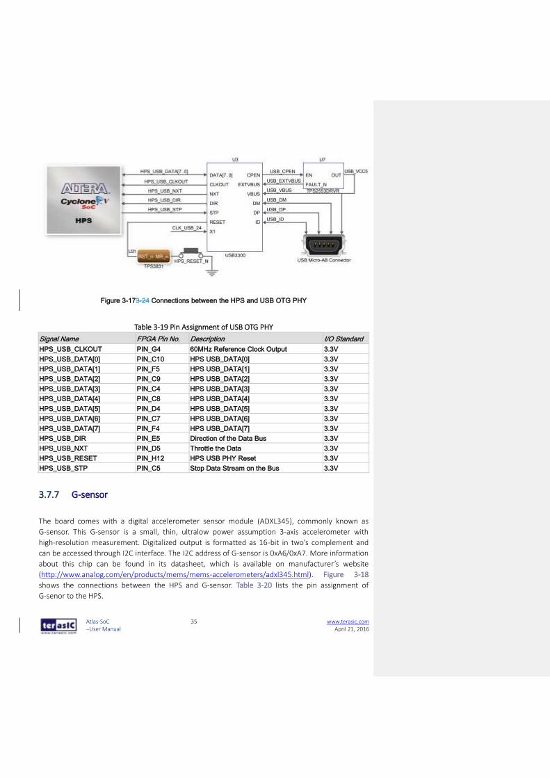
33..77..66 UUSSBB 22..00 OOTTGG PPHHYY
The board provides USB interfaces using the SMSC USB3300 controller. A SMSC USB3300 device in a
32-pin QFN package device is used to interface to a single Type AB Micro-USB connector. This device
supports UTMI+ Low Pin Interface (ULPI) to communicate to USB 2.0 controller in HPS. As defined
by OTG mode, the PHY can operate in Host or Device modes. When operating in Host mode, the
interface will supply the power to the device through the Micro-USB interface. Figure 3-17 shows
the connections of USB PTG PHY to the HPS. Table 3-19 lists the pin assignment of USB OTG PHY to
the HPS.
Atlas-SoC User Manual
35 www.terasic.com April 21, 2016
Figure 3-173-24 Connections between the HPS and USB OTG PHY
Table 3-19 Pin Assignment of USB OTG PHY
Signal Name FPGA Pin No. Description I/O Standard
HPS_USB_CLKOUT PIN_G4 60MHz Reference Clock Output 3.3V
HPS_USB_DATA[0] PIN_C10 HPS USB_DATA[0] 3.3V
HPS_USB_DATA[1] PIN_F5 HPS USB_DATA[1] 3.3V
HPS_USB_DATA[2] PIN_C9 HPS USB_DATA[2] 3.3V
HPS_USB_DATA[3] PIN_C4 HPS USB_DATA[3] 3.3V
HPS_USB_DATA[4] PIN_C8 HPS USB_DATA[4] 3.3V
HPS_USB_DATA[5] PIN_D4 HPS USB_DATA[5] 3.3V
HPS_USB_DATA[6] PIN_C7 HPS USB_DATA[6] 3.3V
HPS_USB_DATA[7] PIN_F4 HPS USB_DATA[7] 3.3V
HPS_USB_DIR PIN_E5 Direction of the Data Bus 3.3V
HPS_USB_NXT PIN_D5 Throttle the Data 3.3V
HPS_USB_RESET PIN_H12 HPS USB PHY Reset 3.3V
HPS_USB_STP PIN_C5 Stop Data Stream on the Bus 3.3V
33..77..77 GG--sseennssoorr
The board comes with a digital accelerometer sensor module (ADXL345), commonly known as
G-sensor. This G-sensor is a small, thin, ultralow power assumption 3-axis accelerometer with
high-resolution measurement. Digitalized output is formatted as 16-bit in two’s complement and
can be accessed through I2C interface. The I2C address of G-sensor is 0xA6/0xA7. More information
about this chip can be found in its datasheet, which is available on manufacturer’s website
(http://www.analog.com/en/products/mems/mems-accelerometers/adxl345.html). Figure 3-18
shows the connections between the HPS and G-sensor. Table 3-20 lists the pin assignment of
G-senor to the HPS.

Atlas-SoC User Manual
36 www.terasic.com April 21, 2016
Figure 3-183-25 Connections between Cyclone V SoC FPGA and G-Sensor
Table 3-20 Pin Assignment of G-senor
Signal Name FPGA Pin No. Description I/O Standard
HPS_GSENSOR_INT PIN_A17 HPS GSENSOR Interrupt Output 3.3V
HPS_I2C0_SCLK PIN_C18 HPS I2C0 Clock 3.3V
HPS_I2C0_SDAT PIN_A19 HPS I2C0 Data 3.3V
33..77..88 LLTTCC CCoonnnneeccttoorr
The board has a 14-pin header, which is originally used to communicate with various daughter cards
from Linear Technology. It is connected to the SPI Master and I2C ports of HPS. The communication
with these two protocols is bi-directional. The 14-pin header can also be used for GPIO, SPI, or I2C
based communication with the HPS. Connections between the HPS and LTC connector are shown in
Figure 3-19, and the pin assignment of LTC connector is listed in Table 3-21.

Atlas-SoC User Manual
37 www.terasic.com April 21, 2016
Figure 3-193-26 Connections between the HPS and LTC connector
Table 3-21 Pin Assignment of LTC Connector
Signal Name FPGA Pin No. Description I/O Standard
HPS_LTC_GPIO PIN_H13 HPS LTC GPIO 3.3V
HPS_I2C1_SCLK PIN_B21 HPS I2C1 Clock 3.3V
HPS_I2C1_SDAT PIN_A21 HPS I2C1 Data 3.3V
HPS_SPIM_CLK PIN_C19 SPI Clock 3.3V
HPS_SPIM_MISO PIN_B19 SPI Master Input/Slave Output 3.3V
HPS_SPIM_MOSI PIN_B16 SPI Master Output /Slave Input 3.3V
HPS_SPIM_SS PIN_C16 SPI Slave Select 3.3V

Atlas-SoC User Manual
38 www.terasic.com April 21, 2016
Chapter 4
Appendix B
4.1 RReevviissiioonn HHiissttoorryy
Version Change Log
V1.0 Initial Version (Preliminary)
V1.1 Minor corrections: fixing Table 3-2.
V1.2 Add GPIO pin Arrangement (Figure 3-18)
4.2 CCooppyyrriigghhtt SSttaatteemmeenntt
Copyright © 2015 Terasic Inc. All rights reserved.